
Chapter 10
Printed Circuit Board Layout
This chapter covers printed circuit board (PCB) layout for switching power supplies. It reveals how to analyze any topology for its critical trace sections and describes how to ensure the constructed power supply behaves as it was intended to. Techniques to reduce inductances and to correctly parallel output capacitors in a flyback are presented. An introduction into thermal aspects of PCB design is also included to pave the way for a more detailed discussion into thermal management aspects in general, in the following chapter.
Introduction
A great many customer “complaints” regarding switcher ICs are ultimately traced to poor printed circuit board (PCB) layout practices. When designing a PCB for a switching regulator, we need to be aware that the final product is going to be only as good as its layout. Certainly, some ICs are more noise-sensitive than others. Sometimes, the “same” part from several vendors can also have starkly varying noise sensitivities. Further, some ICs are architecturally more noise-sensitive than others (e.g., current-mode controllers are far more “layout-sensitive” than voltage-mode controllers). We also have to face the fact that virtually no semiconductor manufacturers characterize the noise sensitivity of their products (often letting the customers discover it for themselves!). However, as designers, we can certainly, with poor attention to layout, pull off the near-impossible — turn a comparatively stable IC into a jittery and nervous part — one that can malfunction and even cause catastrophic consequences (switch failure). Further, since very few of these problems can be easily corrected, or “band-aided,” at a later stage, it is very important to get the layout right at the very beginning.
Most of the layout recommendations in this chapter revolve around simply ensuring basic functionality and performance. Though luckily, the beleaguered switcher designer will be happy to know, in general, the electrical aspects are all related — pointing in the same general direction. So, for example, a good layout, that is, one that helps the IC function properly, also leads to reduced electromagnetic emissions, and vice versa. There are some exceptions to this trend however, particularly when it comes to the practice of indiscriminate “copper-filling” (or copper “flooding”) on PCBs, which we will touch upon later. Subsequently, the reader can try to gain more insight into the practical aspects of making switching regulators, by reading the chapters dedicated to the topic of EMI, later in this book.
Trace Section Analysis
A switch transition (crossover) occurs when the switch changes from an on-state (switch closed) to an off-state (switch open), or back. A typical transition lasts typically less than 100 ns. But most of the trouble starts right here! In fact, the noise has comparatively little to do with the basic switching frequency of the converter itself — it is the transition that is responsible for most of the noise and all its attendant problems. The smaller the switch transition time, the more the possible consequences, as we will see.
The first requirement for the designer is to understand the flow of power-related currents in the converter. This leads to an identification of the troublesome or “critical” traces of the PCB; we must pay the closest attention to these traces. We will also see that this identification process is very “topology-dependent.” So we can’t, for example, design the PCB for a Buck-Boost, the same way we would do it for a Buck. The rules change significantly! We may thus also realize that very few PCB layout persons out there would understand this too well! Therefore, it really is a good idea for the power supply designer to do the layout personally, or at the very least, closely supervise the PCB person in the act.
Some Points to Keep in Mind During Layout
Let’s summarize these for quick reference purposes:
• During a crossover transition, the current flow in certain trace sections has to suddenly come to a stop, and in certain others it has to start equally suddenly (within 100 ns or less typically, which is the switch transition time). These trace sections are identified as the “critical traces” in any switcher PCB layout. A very high dI/dt is created in them, during every switch transition (see Figure 10.1). Expectedly, these traces end up “complaining” vociferously in the form of small, but potent, voltage spikes across them. If Chapter 1 has been fully understood by now, we realize that this is just the equation V=L×dI/dt playing out its part — with the “L” being the parasitic inductance of the PCB trace. The rule of thumb for the inductance presented by a trace is 20 nH per inch of trace length.
• Once generated, these noise spikes can not only appear at the input/output (causing performance issues), but also infiltrate the IC control section, causing it to behave anomalously, and unpredictably. We, for example, could even end up briefly losing current-limiting function, leading to disastrous consequences.
• MOSFETs switch faster than “BJTs” (bipolar junction transistors). The transition times of a MOSFET can be of the order of 10–50 ns, as compared to a BJT’s 100–300 ns. But that also makes the “spikes” far more severe in the case of the converters that use MOSFET switches — because of the much higher dI/dt’s they can generate in the critical trace sections of the PCB.
Note: One inch of trace switching, say 1 A of instantaneous current in a transition time of 30 ns, gives a spike of 0.7 V. For 3 A, and 2 in. of trace, the induced voltage tries to be 4 V!
Note: It is almost impossible to “see” the noise spikes. First of all, various parasitics help limit/absorb them somewhat (though they can still retain the capability to cause “controller upset”). Further, the moment we put in an oscilloscope probe, the 10–20 pF of probe capacitance can also absorb the spikes, and we would probably see nothing significant. In addition, probes pick up so much normal switching noise through the air anyway that we are never completely sure what we are seeing!
• Integrated switchers ICs (or simply “switchers”) have the switch in the same package as the control. Though that makes for convenience and low parts count, such ICs are usually more sensitive to the noise spikes generated by the parasitic trace inductances. That is because the “switching node” of the power stage (its “swinging node,” i.e., the one connecting the diode, switch, and inductor) is a pin on the IC itself so that the pin conducts any unusual high-frequency noise at the switching node straight into the control sections, causing “controller upset.”
• Note that while prototyping, it is a bad idea to insert a current probe (through a loop of wire) anywhere in a critical path (learn to recognize these in Figure 10.1). The current loop becomes an additional inductance that can increase the amplitude of the noise spikes dramatically. Therefore, practically speaking, it often becomes virtually impossible to measure the switch current or the diode current individually (especially in the case of switcher ICs). In such cases, only the inductor current waveform can really be measured properly.
• Note that in the Buck and the Buck-Boost, the input capacitor is also included in a critical path. That implies we need very good input decoupling in these topologies (for the power section). So, besides the necessary bulk capacitor for the power stage (typically a tantalum or aluminum electrolytic of large capacitance), we should also place a small ceramic capacitor (about 0.1–1 μF) directly between the quiet end of the switch (i.e., at the supply side) and the ground — and also as close as possible to the switch.
• In Figure 10.1, the control section (IC) has not been shown. However, we should remember that the control circuitry usually needs good local decoupling of its own. And for that we need to provide a small ceramic capacitor very close to the IC. Clearly, especially when dealing with switchers, the decoupling ceramic for the power stage can often do “double duty” as the decoupling capacitor of the control too (note that this applies to the Buck-Boost and the Buck only, since the input power-decoupling capacitor is required only for them).
• Sometimes, more effective control IC decoupling may be required — in which case we can use a small resistor (typically 10–22 Ω) from the input (supply) rail, going to a (separate) ceramic capacitor placed directly across the input and ground pins of the IC. This constitutes a small “RC filter” for the IC supply.
• Note that in all topologies, the inductor is not in the critical path. So we need not worry much about its layout, at least not from the point of view of noise. However, we have to be wary of the electromagnetic field the inductor creates, because that can impinge on nearby circuitry and sensitive traces, and cause similar (though usually not so acute) problems. So generally, it is a good idea to try to use “shielded inductors” for that reason, if cost permits. If not, it should be positioned a little further from the IC, in particular keeping clear of the feedback trace.
• In the Boost and the Buck-Boost, we see that the output capacitor is in the critical path. So this capacitor should be close to the control IC, along with the diode. A paralleled ceramic capacitor can also help, provided it does not cause loop instability issues (especially in voltage-mode control — see Chapter 12).
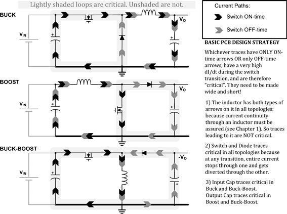
Figure 10.1: Identifying the critical trace sections for the three topologies.
In the Buck, however, note that though the output diode needs to be positioned close to the IC/switch, the output capacitor is not critical (its current is smoothened by the inductor). If we place a ceramic capacitor in parallel to the output capacitor, it is only for the purpose of decreasing high-frequency noise and ripple at the output even further. But it is really not mandatory and can cause loop instability, particularly with voltage-mode control, especially if the effective series resistance (ESR) of the output capacitor section becomes too low (less than 100 mΩ typically).
• The position of the diode is critical in all topologies. It leads to the switching node and from there on, straight into the IC when using switcher ICs. However, in Buck converter layouts in which the diode has unfortunately been placed a little too far away from the IC, the situation can sometimes be rectified, even at a later stage, by means of a small series RC snubber connected between the switching node and ground (across the catch diode, close to the IC). This RC typically consists of a resistor (low-inductive type preferred), of value 10–100 Ω, and a capacitor (preferably ceramic), of value about 470 pF to 2.2 nF. Note that the dissipation in the resistor is ![]() . So not only should the wattage of the resistor be appropriate for the job, but also the capacitance should not be increased indiscriminately, to avoid compromising the efficiency significantly.
. So not only should the wattage of the resistor be appropriate for the job, but also the capacitance should not be increased indiscriminately, to avoid compromising the efficiency significantly.
• A first approximation for the inductance of a conductor (wire) having length I and diameter “d” is
![]()
where l and d are in centimeters. Note that the equation for a PCB trace is not much different from that of a wire.
![]()
where “w” is the width of the trace in cm. Note that for PCB traces, the inductance hardly depends on the thickness of the copper on the board.
• The logarithmic relationship above indicates that if we halve the length of a PCB trace, we can make its inductance halve too. But we have to increase its width almost 10 times, to get its inductance to halve. In other words, simply making traces “wide” may not do much — we need to keep trace lengths short.
• The inductance of a “via” (through-hole) is given by
![]()
Here “h” is the height of the via in millimeters (equal to the thickness of the board, commonly 1.4–1.6 mm) and “d” is the diameter of the via in millimeters. Therefore, a via of diameter 0.4 mm on a 1.6 mm thick board gives an inductance of 1.2 nH. That may not sound like much, but it has been known to cause problems in switcher ICs, especially those using MOSFETs. Because of their fast transition times, input ceramic decoupling capacitors for such ICs become almost mandatory. Therefore, it is strongly advised that this input ceramic capacitor be placed extremely close to where the pins of the IC actually contact the board. There should be no intervening vias between this capacitor and the solder pads of the pins as this worsens decoupling significantly.
• Increasing the width of certain traces can in fact become counterproductive. For example, for the (positive) Buck regulator, the trace from the switching node to the diode is “hot” (swinging). Any conductor with a varying voltage on it, irrespective of the current it may be carrying, becomes an E-field antenna if its dimensions are large enough. Therefore, the area of the copper around the switching node needs to be reduced, not increased. That is why we need to avoid the tendency of indiscriminate “copper-filling” — the only voltage node that really qualifies for copper-filling is the ground node (or plane). All others, including the input supply rail, can start radiating significantly because of the high-frequency noise riding on them. By making large planes, we also increase the probability of that plane picking up noise from nearby traces and components, by means of inductive and capacitive coupling.
• The so-called “1-oz” board in the United States is actually equivalent to 1.4-mils copper thickness (or 35 μm) on the board. Similarly “2 oz” is twice that. For a moderate temperature rise (less than 30°C) and currents less than 5 A, we can use a minimum 12-mils width of copper per Ampere for 1-oz board, and at least 7-mils width of copper per amp for a 2-oz board. This rule of thumb is based on the DC resistance of the trace only. So to decrease its inductive impedance and AC resistance, higher trace widths may be required.
• We have seen that the preferred method to reduce trace inductance is to reduce length, not increase width. Beyond a certain point, widening of traces does not reduce inductance significantly. Nor does it depend much on whether we use 1-oz or 2-oz boards. Nor if the trace is “unmasked” (to allow solder/copper to deposit and thereby increase effective conductor thickness). So, if for any reason, the trace length cannot be reduced further, another way to reduce inductance is by paralleling the forward and return current traces. Inductances exist because they represent stored magnetic energy. The energy resides in the magnetic field. Therefore, conversely, if the magnetic field could be canceled, the inductance vanishes. By paralleling two current traces, each carrying currents of the same magnitude but in opposite direction, the magnetic field is greatly reduced. These two traces should be parallel and very close to each other on the same side of the PCB. If a double-sided PCB is being used, the best solution is to run the traces parallel (over each other) on opposite sides (or adjacent layers) of the PCB. These traces can, and should, be fairly wide to improve mutual coupling and thereby the field cancellation. Note that if a ground plane is used on one side, the return path automatically “images” the forward current trace (for high frequencies), and produces the sought-after field cancellation.
• In high-power off-line flybacks, the trace inductances on the secondary side reflect on to the primary side, and can greatly increase the effective primary-side leakage inductance and impair the efficiency (see Chapter 3). The situation gets worse when we have to stack several output capacitors in parallel, just to handle the higher RMS currents — long traces seem inevitable here. However, one way to decrease the inductance is by the field cancellation principle discussed above. This is shown implemented in Figure 10.2. Two copper planes (or big copper islands) are allocated, starting from the output diode. One of these planes is the ground plane, the other being the output voltage rail. By using two large parallel planes carrying forward and return currents, the inductance almost completely cancels out, and leads to a very good high-frequency freewheeling path as desired. Note that in the bargain, we also get excellent current sharing between the output capacitors.
• In single-sided boards, a popular way to ensure current sharing between several paralleled output capacitors is shown in Figure 10.3. It doesn’t minimize inductance, but it does ensure that the life of the first downstream capacitor does not come to a premature end (simply because of “current hogging”). Note that in the “improved” layout on the right side of the figure, the total distance from the diode through each capacitor is roughly equal in all three cases shown — thus leading to more precise sharing.
• With multilayer boards, it is a common practice to almost completely fill one layer with ground (if so, it should preferably be the layer immediately below the power components/traces). There are people who, usually rightly so, consider this a panacea for most problems. As we have seen, every signal has a return, and as its harmonics get higher, the return current, rather than trying to find the path of least DC resistance (straight line), tries to reduce the inductance by imaging itself directly under the signal path even though that may be “zigzagging” away on the board. So by leaving a large ground plane, we basically “allow” nature to “do its thing” — searching and finding the path of least impedance (lowest DC resistance or lowest inductive impedance, depending upon the frequency of the harmonic). The ground plane also helps thermal management as it couples some of the heat to the other side. The ground plane can also capacitively link to noisy traces above it, causing general reduction in noise/EMI. However, it can also end up radiating if caution is not exercised. One way this can happen is to have too much capacitive coupling from noisy traces. No ground plane is perfect, and when we inject noise into it, it may get affected, especially if the copper is too thin. Also, if the ground plane is partitioned in odd ways, either to create thermal islands, or to route other traces, the current flow patterns can become irregular. No longer can return paths in the ground plane pass directly under their forward traces. The ground plane can then end up behaving as a slot antenna in terms of EMI.
• The only important signal trace to consider is usually the feedback trace. If this trace picks up noise (capacitively or inductively), it can lead to slightly offset output voltages — and in extreme cases (though rare), even instability or device failure. We need to keep the feedback trace short if possible so as to minimize pickup and keep it away from noise or field sources (the switch, diode, and inductor). We should never pass this trace under the inductor, or under the switch or diode (even if on opposite sides of the PCB). We should also not let it run close to and parallel, for more than a few millimeters at most, to a noisy (critical) trace, even on adjoining layers of the board. Though if there is an intervening ground plane that should provide enough shielding between layers.
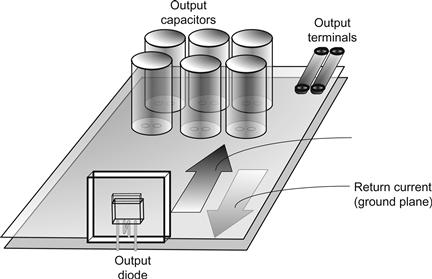
Figure 10.2: How to achieve low-inductance connections to output capacitors of a flyback.
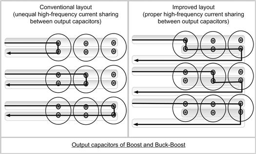
Figure 10.3: How to get output capacitors of a flyback to share current.
Keeping the feedback trace short may not always be physically feasible. We should realize that keeping it short certainly is not of the highest priority. In fact, we can often deliberately make it long, just so that we can assuredly route it away from potential noise sources. We can also judiciously cut into the “quiet” ground plane to pass this particular trace through so that in effect, it is surrounded by a “sea of tranquility.”
Thermal Management Concerns
Larger and larger areas of copper do not help, especially with thinner copper. A point of diminishing returns is reached for a square copper area of size 1 in.×1 in. Some improvement continues until about 3 in. (on either side), especially for 2-oz boards and better. But beyond that, external heatsinks are required. A reasonable practical value attainable for the thermal resistance (from the case of the power device to the ambient) is about 30°C/W. That means 30°C rise for every Watt of dissipation.
To calculate the required copper area, we can use as a good approximation the following empirical equation for the required copper area:
![]()
Here P is in Watts and Rth is the desired thermal resistance in °C/W.
For example, suppose the estimated dissipation is 1.5 W. We want to ensure that, at a worst-case ambient of 55°C, the case of the part does not rise above 100°C (safe temperature for the PCB material — do not exceed!). Therefore, the Rth we are looking for here is
![]()
Therefore, the required copper area is
![]()
If this area is square in shape, the length of each side needs to be 6.790.5=2.6 in. We can usually make this somewhat rectangular or odd-shaped too, as long as we preserve the total area. Note that if the area required exceeds 1 sq.in., a 2-oz board should be used (as in this case). A 2-oz board reduces the thermal “constriction” around the power device and allows the large copper area to be more effectively used for natural convection.
We should not think that heat is lost only from the copper side. The usual laminate (board material) used for SMT (surface mount technology) applications is epoxy-glass “FR4,” which is a fairly good conductor of heat. So some of the heat from the side on which the device is mounted does get across to the other side, where it contacts the air and helps lower the thermal resistance. Therefore, just putting a copper plane on the other side also helps — but only by about 10–20%. Note that this “opposite” copper plane need not even be electrically the same point — it could, for example, just be the usual ground plane. A much greater reduction of thermal resistance (by about 50–70%) can be produced if a cluster of small vias (“thermal vias”) is employed to conduct the heat from the component side to the opposite side of the PCB.
Thermal vias, if used, should be small (0.3–0.33 mm barrel diameter) so that the hole is filled up during the plating process. Too large a hole can cause “solder wicking” during the reflow soldering process, which leads to a lot of solder getting sucked into the holes, thereby creating bad solder joints for components in the vicinity. The “pitch” (i.e., the distance between the centers) of several such thermal vias in a given area is typically 1–1.2 mm. A grid of several such vias can be placed very close to, and alongside, a power device, and even under its tab (if present). See Chapter 11 for thermal management concerns in more detail.