Chapter Seventeen. Electronic Diagrams
Objectives
After studying the material in this chapter, you should be able to:
1. Identify common component symbols on an electronic schematic diagram.
2. Draw a schematic diagram using standardized symbols.
3. Draw connecting and crossover paths.
4. Identify interrupted and uninterrupted lines.
5. Designate terminals and numerical values of components.
Refer to the following standards:
• ANSI/IEEE 200 Graphic Symbols for Electrical and Electronic Diagrams
• ASME/IEEE 91/91A Graphic Symbols for Logic Functions (Includes IEEE Std 91A Supplement, and IEEE Std 91)
• ASME/IEEE 315 Graphic Symbols for Electrical and Electronics Diagrams (Includes 315A Supplement)
• ASME 14.24 Types and Applications of Engineering Drawings

A Mobile Phone Transmitter Atop a Building in Chicago, Illinois (Courtesy of Roger Tully/Stone Allstock/Getty Images.)
Understanding Electronic Diagrams
Figure 17.1 shows a schematic diagram. Figure 17.2 shows a first-floor lighting diagram for an architectural project. There are a wide variety of electrical and electronic drawings and diagrams. As is the case in all types of technical drawing, you will need to become familiar with specialized industrial practice for the drawings you prepare. A wiring diagram for a second-floor house plan looks quite different from a logic diagram. This chapter is intended to introduce you to the types of drawings and general practices and symbols used in electronic diagrams.

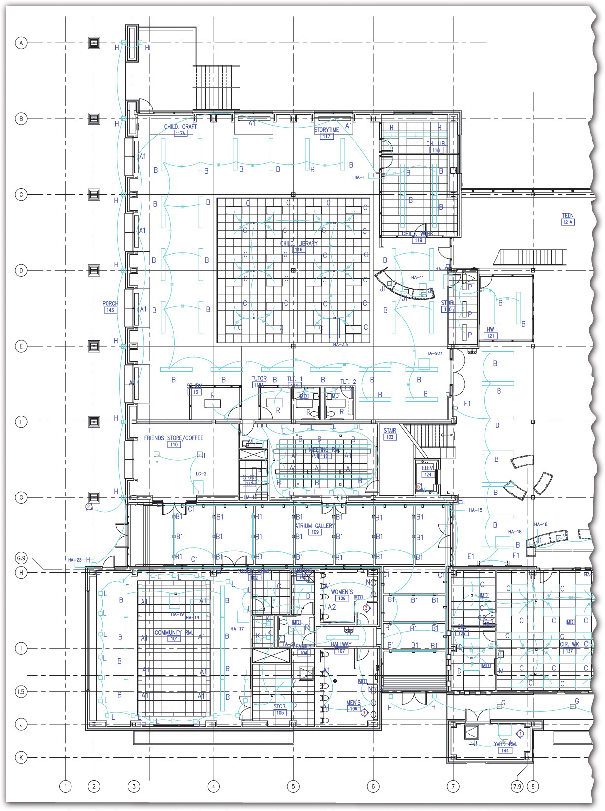
17.2 Portion of a Single-Line Diagram Showing the First-Floor Lighting Plan for a Public Library (Courtesy of Associated Construction Engineering.)
Standard Symbols
The symbols approved by the American National Standards Institute (ANSI) are published in Graphic Symbols for Electrical and Electronic Diagrams, ANSI/IEEE 200. In addition, modern printed circuitry techniques, which are used extensively in electronic equipment, require specially prepared diagrams or drawings. Much of the material in this chapter is extracted or adapted from that standard.
Other standards should be referred to as required. The U.S. government has developed a series of standards to be used by military contractors, for example MIL-STD-681 Identification Coding and Application of Hook Up and Lead Wires. In other applications, adherence to standards developed by Underwriters’ Laboratory (UL) may be required, particularly where safety considerations may dictate a special printed circuit board layout or component spacing. Standards are updated as they evolve, so research the current applicable standards for the type of drawing you are creating.
CAD Symbol Libraries
You can create or purchase libraries of standard electronic symbols for use in electronic diagrams. CAD symbol libraries should follow approved standards just as manually created drawings would. When you create CAD drawings showing electronic symbols, consider the final size of the plotted drawing. Make sure that symbols you create or add to drawings meet minimum size standards as set out in ASME Y14.2.
Types of Electronic Diagrams
The following are types of diagrams defined in ASME Y14.24 that are commonly used in the electronics industry.
Functional block diagram A functional block diagram shows the functions of major elements in a circuit, assembly, or system using a simplified form. It is used to simplify the representation of complex equipment by using blocks or rectangles to depict stages, units, or groups of components in a system (Figure 17.3).
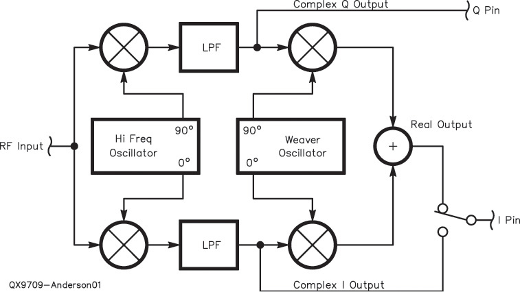
17.3 Functional Block Diagram for a Digital Downconverter (Courtesy of September 1997 QEX: Copyright ARRL.)
Single-line diagram A single-line diagram shows the path of an electrical/electronic circuit in a general format using single lines and symbols (Figure 17.4).
Schematic or circuit diagram A schematic diagram or circuit diagram shows the electrical connections and functions of a specific circuit arrangement. It does not depict the physical shape, size, or arrangement of the elements. This type of drawing is used to communicate the design, construction, and maintenance information for electronic equipment. It facilitates tracing the circuit to convey its function (Figure 17.5).

17.5 Schematic Diagram of a FET (field-effect transistor) VOM (volt-ohm-milliammeter) (Courtesy of American Radio Relay League.)
Connection or wiring diagram A connection or wiring diagram shows the connections of an installation or its component devices or parts. It may cover internal or external connections, or both, and contains the level of detail to show the connections involved. The connection diagram usually shows general physical arrangement of the component devices or parts. This type of diagram is used to represent the wiring between component devices in electrical or electronic equipment (Figure 17.6).

Interconnection diagram An interconnection diagram shows only external connections between unit assemblies or equipment. The internal connections of the unit assemblies or equipment are usually omitted. This diagram is similar to the connection diagram; both serve to supplement schematic diagrams.
17.1 Drawing Size, Format, and Title
The title should include the standardized wording for the type of the drawing and a description of the application, for example:
SINGLE-LINE DIAGRAM—AM–FM RECEIVER SCHEMATIC
DIAGRAM—250-WATT AMATEUR TRANSCEIVER
It is often useful to include some basic wiring information on schematic diagrams, such as connection details of transformers and switches. For combined forms such as this, do not alter the title, but describe the primary function of the diagram.
17.2 Line Conventions and Lettering
As in any drawing for reproduction, select line thicknesses and letter sizes according to the amount of reduction or enlargement involved so that all parts of the drawing will be legible.
ASME recommends a line of medium thickness for general use on electrical diagrams. A thin line may be used for brackets, leader lines, and so on. To emphasize special features such as main signal paths, a thicker line may be used to provide the desired contrast. For recommended line thickness and lettering, refer to ASME Y14.2M.
Line conventions for electrical diagrams are shown in Figure 17.7. Lettering on electrical diagrams should meet the same standards as for other drawings. For most sheet sizes, a letter height of 3 mm (.125″) is typical.
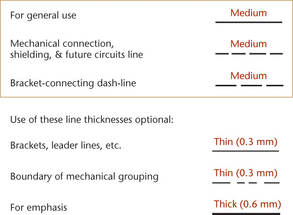
17.7 Line Conventions for Electronic Diagrams (Reprinted from ASME Y14.2, by permission of The American Society of Mechanical Engineers. All rights reserved.)
17.3 Standard Symbols for Electronic Diagrams
Symbols Symbols should conform to an internationally or nationally approved standard, such as IEEE 315, a portion of which is shown in Figure 17.8. On rare occasions when no standard symbol is available, you can devise a special symbol (or augment a standard symbol), provided that you include an explanatory note. Appendix 35 provides many common schematic symbols for electrical/electronic diagrams.

17.8 A Portion of the Standard Showing Graphic Symbols for Electrical and Electronics Diagrams (Courtesy of IEEE.)
Size of symbols Symbols should be drawn roughly 1.5 times the size of those shown in the IEEE 315 standard. The relative proportions of the symbols and relative sizes compared with one another should be maintained. If the drawing will be printed at a reduced scale, the symbols must be larger, so that when reduced they will still be completely legible. Following this recommendation, circular envelopes for semiconductors will be about 16 mm (or .62″) to 19 mm (or .75″) in diameter, although the envelope for semiconductors may be omitted if no confusion results.
Switches and relays Switches and relays should be shown in the “normal” position—with no operating force or applied energy. If exceptions are necessary, as for switches that may operate in several positions with no applied force, describe the conditions in an explanatory note on the drawing.
17.4 Abbreviations
Abbreviations on electrical diagrams should conform to ASME Y14.38. (See Appendix 2.)
17.5 Grouping Parts
When parts or components are naturally grouped, as in separately obtained sub-assemblies or assembled components such as relays, tuned circuit transformers, hermetically sealed units, and printed circuit boards, indicate the group using a dashed line to enclose them in a “box,” as in Figure 17.9. You can also group components by showing extra space from adjacent circuitry.
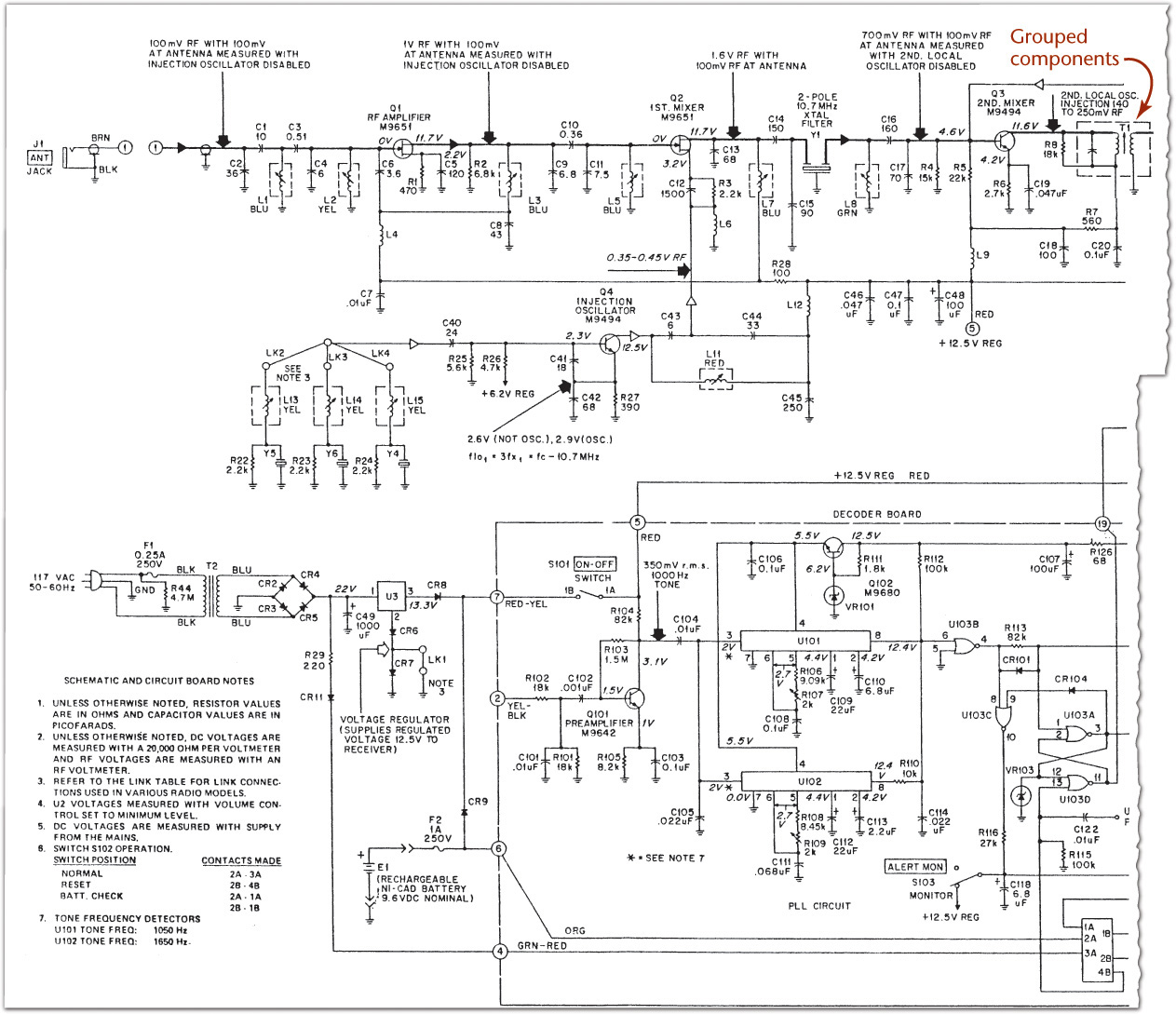
17.9 Portion of a Maintenance-Type Schematic Diagram of FM Weather Monitor Radio (Copyright Motorola, Inc. 1980. All rights reserved.)
17.6 Arrangement of Electrical/Electronic Symbols
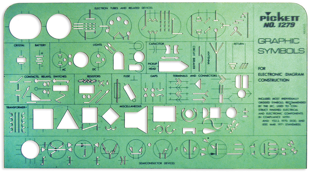
Figure 17.10 shows a freehand sketch of a schematic diagram. It helps to use grid paper when sketching schematics, because it is easier to keep components lined up and makes a neater sketch. Rearrange details to improve the final diagram if it is redrawn. Templates, such as the one shown in Figure 17.11, save time when drawing symbols.

CAD can help you to produce complicated schematic drawings efficiently. As a minimum, CAD software provides standard symbol libraries that make it quick to place the symbols into a drawing. On the more complex side, CAD packages may automatically route traces and simulate the circuit function. Figure 17.12 shows an example drag-and-drop CAD symbol palette. Figure 17.13 shows symbols in circuit simulation software.
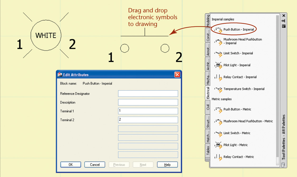
17.12 AutoCAD Software Provides a Convenient Tool Palette for Inserting Symbols (Autodesk screen shots reprinted courtesy of Autodesk, Inc.)
17.13 A Simple Circuit Design Created in OrCAD. Circuits created in OrCAD allow simulation of their function. (Courtesy of Cadence® Design Systems, Inc. OrCAD® is a registered trademark of Cadence Design Systems, Inc.)
Symbol Arrangement
Arrange the various parts and symbols to balance blank areas and lines. Provide sufficient blank space adjacent to symbols to allow for reference designations and notes. Exceptionally large spaces give an unbalanced effect but may be necessary to provide for later circuit additions. Of course, using CAD, it is easy to move and stretch the existing drawing to add space.
Signal Path
Arrange schematic and single-line diagrams so that the signal or transmission path from input to output proceeds from left to right and from top to bottom when possible. Supplementary circuits, such as a power supply or an oscillator circuit, are usually drawn below the main circuit.
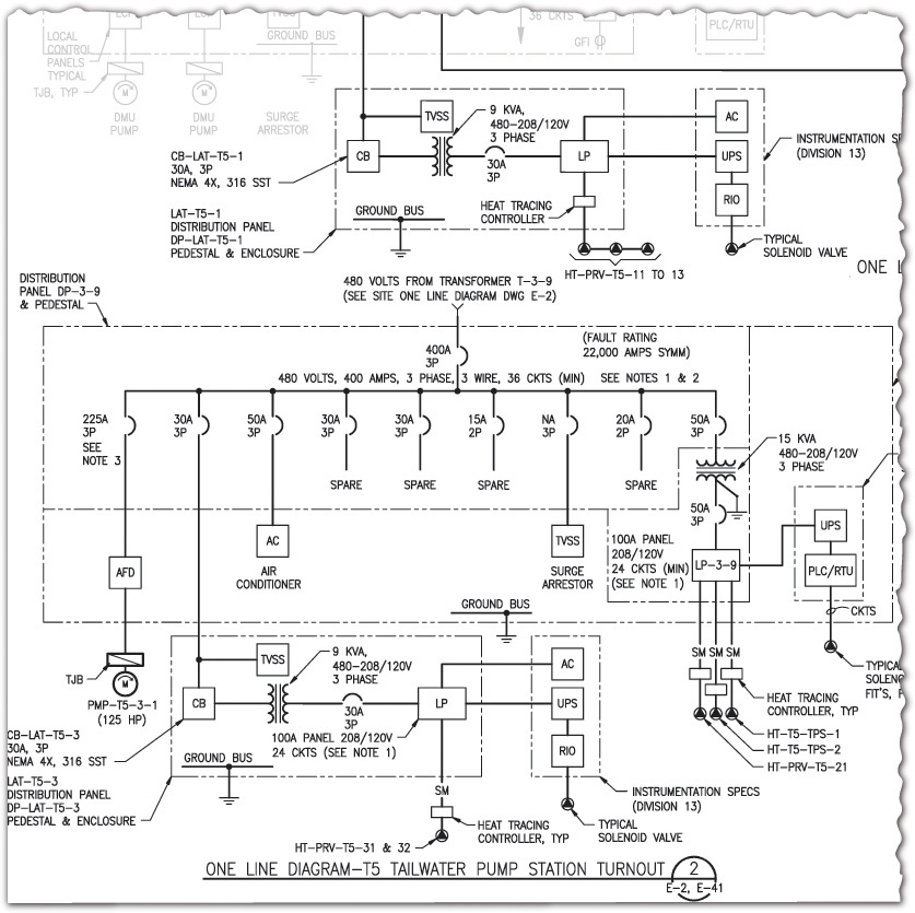
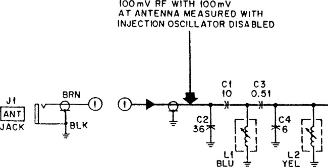
Stages of an electronic device are groups of components or a semiconductor, which together perform one function of the device. For example, the sketch in Figure 17.10 shows the RF (radio frequency) amplifier stage of the FM Weather Monitor Radio, whose schematic was shown in Figure 17.9. Other stages that can be seen in Figure 17.9 are the first and second mixer stages associated with transistors Q2 and Q3; the limiter/detector stage, containing integrated circuit U1; and finally the audio output stage, U2, and speaker. The power supply, which rectifies alternating current through diodes CR2–CR5 to produce direct current voltage, regulated through integrated circuit U3, is shown at the lower left, along with a rechargeable battery backup power supply, E1.
Also shown in the lower portion of the diagram is the circuitry contained on a separate tone decoder printed circuit board (within the dashed lines).
With experience in drawing electronic circuits you are able to visualize fairly accurately the space required by the circuitry involved in each stage. Generally, you should keep the semiconductor symbols arranged in horizontal lines and group the associated circuitry in a reasonably symmetrical arrangement about them. This way each stage is confined to an area of the drawing.
Note that the signal path from input to output follows from left to right and top to bottom. The input is at the upper left and the output at the lower right in Figure 17.9. The signal path is clearly designated by a heavier-than-normal line. This is typical of maintenance-type schematic diagrams, which are drawn to be easily read and interpreted by service technicians. Heavier lines in the drawing are used for emphasis but do not have any other significance. Supplementary circuitry (in this case the power supply) is in the lower portion of the diagram.
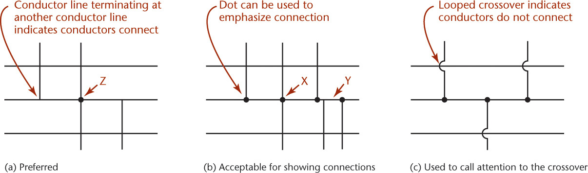
17.7 Connections and Crossovers
Connecting lines (for conductors) are typically drawn horizontally or vertically, minimizing bends and crossovers. Avoid using long interconnecting lines. You can use interrupted paths to prevent the need for long, awkward interconnecting lines or in cases where a diagram occupies more than one sheet. When parallel connecting lines must be drawn close together, the spacing between lines should not be less than .06″ after reduction. Group parallel lines with similar functions and with at least double spacing between groups to make the drawing easier to interpret.
At times it is impossible to avoid drawing a line representing a conductor wire across another conductor wire, where the wires cross but do not connect. These crossovers must clearly depict that the conductors do not make a connection. Figure 17.14a shows the recommended practice, in which the termination of a line signifies a connection. If more than three lines come together, as at Z, the dot symbol is necessary. You can avoid this by staggering the connecting lines, as in b. The looped crossovers in Figure 17.14c are no longer standard but are still used when there is possibility of confusion.
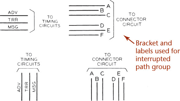
17.8 Interrupted Paths
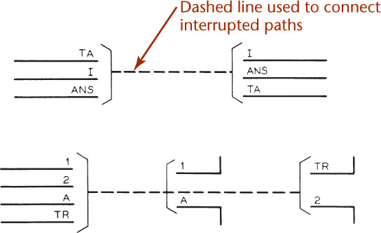
Interrupted paths may be used for either a single line or groups of lines to simplify a diagram (Figures 17.15 and 17.16). Label these carefully with letters, numbers, abbreviations, or other identification so that their destinations are unmistakable. Grouped lines are also bracketed as well as labeled (Figure 17.16). When convenient, interrupted grouped lines may be connected by dashed lines (Figure 17.17).
17.9 Terminals
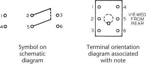
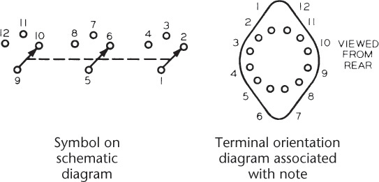
Terminal circles need not be shown unless they are needed for clarity and identification.
When actual physical markings appear on or near terminals of a component, they may be shown on the electrical diagram. Otherwise, assign arbitrary reference numbers or letters to the terminals and add a simple diagram that associates the numbers or letters with the actual arrangement of terminals on the component (Figures 17.18, 17.19, and 17.20b). Figure 17.20a is a pictorial explanation of Figure 17.20b.
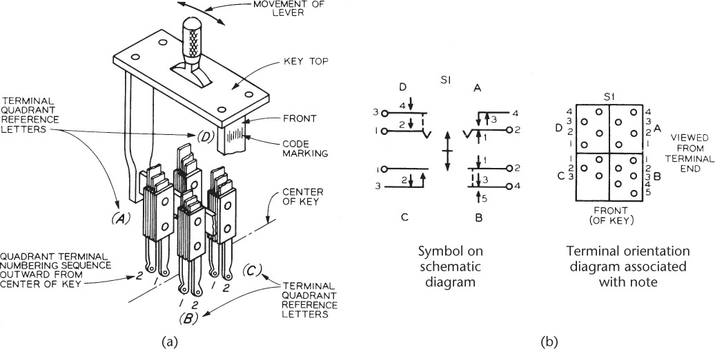
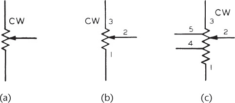
Terminal identification for rotary variable resistors follows similar practices, but it is often desirable to indicate the direction of rotation as well, usually as clockwise or counterclockwise, as viewed from the knob or actuator end of the control. Any other arrangement must be explained by a note or diagram. The letters CW placed near the terminal adjacent to the movable contact identify the extreme clockwise position of the movable terminal (Figure 17.21a). When terminals are numbered, number 2 is assigned to the movable contact (Figure 17.21b). Additional fixed taps are assigned sequential numbers, as in Figure 17.21c.
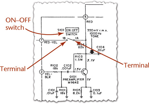
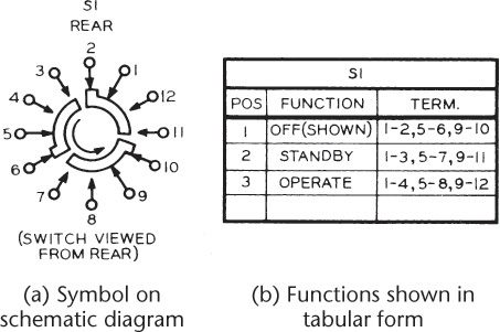
Switch S101 of Figure 17.22 illustrates the use of terminal symbols and their identification. Switch position, as it affects function, should also be shown on a schematic diagram. Depending on complexity, the designation may range from the simple on-off of switch S101 in Figure 17.22 to the functional labeling of the terminals in Figure 17.23a or to the tabular form of function listing in Figure 17.23b.

The tabular forms use dashes to indicate which terminals are connected for each position. For example, in Figure 17.24, position 2 connects terminal 1 to terminal 3, terminal 5 to terminal 7, and terminal 9 to terminal 11.
17.24 Position–Function Relationships for Rotary Switches Using the Tabular Method (Courtesy of IEEE.)
17.10 Color Coding
Terminals or leads are frequently identified by colors or symbols, which should be indicated on the diagram. Figure 17.25 shows how the colors of the insulated wire leads are noted near each terminal. Colors are shown on the drawing using the following codes:
Black: |
BLK |
Blue: |
BLU |
Brown: |
BRN |
Gray: |
GRA |
Green: |
GRN |
Orange: |
ORN |
Red: |
RED |
Violet: |
VIO |
White: |
WHT |
Yellow: |
YEL |
17.11 Division of Parts
For clarity, draw sections of multielement parts separately in a schematic diagram. Indicate subdivisions with suffix letters. For the rotary switch in Figure 17.26, the first portion S1A of switch S1 is identified as S1A FRONT and S1A REAR, viewed as usual from the actuator end.

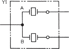
An example using suffixes is shown in Figure 17.27. Here the two piezoelectric crystals A and B are enclosed in one unit, Y1. They are then referred to as Y1A and Y1B.
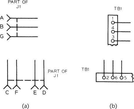
Another way to identify parts of components that are functionally separated on the diagram is with the PART OF prefix (Figure 17.28a). If the portion is indicated as incomplete by a short-break line, as in Figure 17.28b, the words PART OF may be omitted.
17.12 Electron Tube Pin Identification
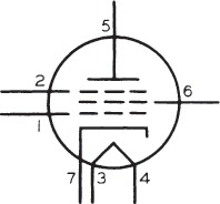
Electron tubes are generally not used in new designs but are still commonly seen in high-power amplifiers. You may see their symbols in maintenance diagrams used while troubleshooting or modifying existing equipment. Electron tube pins are conventionally numbered clockwise from the tube base key or other point of reference, with the tube viewed from the bottom. In the recommended method of pin identification on a diagram, the corresponding numbers are shown immediately outside the tube envelope, adjacent to the connecting line (Figures 17.29 and 17.30).
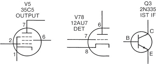
17.30 Reference Designation, Type Number, and Function for Electron Tubes and Semiconductors (Courtesy of IEEE.)
17.13 Reference Designations
In electrical diagrams it is essential to identify each separately replaceable part with appropriate combinations of letters and numbers. Portions not separately replaceable are frequently identified, as in the previous examples. In electronics communications, the recognized form is the appropriate letter followed by a number (the same size and on the same line) with no separating hyphen or space. This is followed by any required suffix, again with no hyphen.
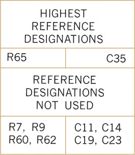
Numbers assigned for each category (resistances, capacitances, inductances, etc.) should start in the upper left corner of the diagram proceeding left to right, then top to bottom, ending at the lower right corner. If parts are deleted in revision, the remaining components should not be renumbered. The numbers not used should be listed in a table (Figure 17.31). If the circuit contains many parts, it may also be helpful to include, as shown, the highest numbers used in each category.
Semiconductors, such as transistors and integrated circuits, are identified by the reference designation and the type number. It is often helpful to include the function below the type number. All this information should be placed near (preferably above) the symbol.
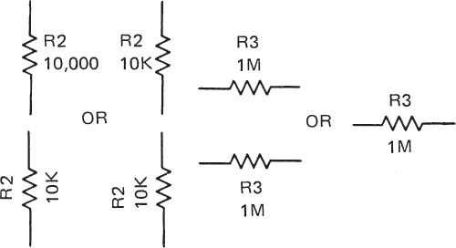
17.14 Numerical Values
Along with reference designations, numerical values for resistance, capacitance, and inductance should be shown, preferably in the form using the fewest numerals. To do this, you can combine the multipliers shown in Figure 17.32a and the symbols in Figure 17.32b and 17.32c. Note that commas are not used in four-digit numbers: 4700 is recommended, not 4,700.
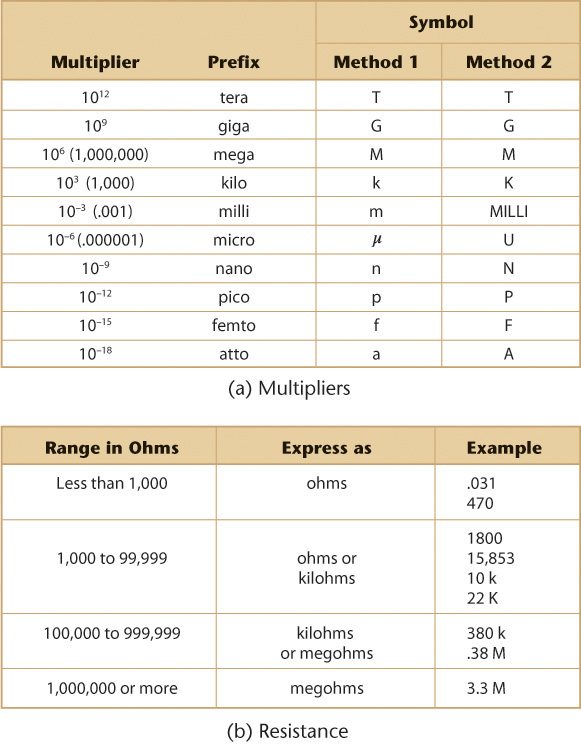
Inductance
According to magnitude, inductance may be expressed in henries (H), millihenries (mH or MILLI H), or microhenries (μH or UH). Following the principle of minimizing the number of numerals, 2μH is preferable to .002 mH, and 5 mH is better than either .005H or 5000 UH.
To avoid repeating measurement units, use a note such as:
UNLESS OTHERWISE SPECIFIED, RESISTANCE
VALUES ARE IN OHMS AND CAPACITANCE
VALUES ARE IN MICROFARADS.
Part Value Placement
For clarity, locate numerical values immediately adjacent to the symbol. Suggested forms are shown in Figure 17.33.
17.15 Functional Identification and Other Information
It sometimes contributes to the readability of a diagram to include special functional identification of certain parts or stages. In particular, where functional designations (TUNER, OUTPUT, etc.) are to be shown on a panel or chassis surface, they should also be shown on the electrical diagram in an appropriate place.
Test points may be identified by the words TEST POINT on the drawing. If several are to be shown, the abbreviated form TP1, TP2, or M1, M2, and so on may be used.
Still other information that may be shown on schematic diagrams, if desired, includes the following:
1. DC resistance of transformer windings and coils
2. Critical input or output impedance values
3. Voltage or current wave shapes at selected points
4. Wiring requirements for critical ground points, shielding pairing, and so on
5. Power or voltage ratings of parts
6. Indication of operational controls or circuit functions
17.16 Integrated Circuits
An integrated circuit is a semiconductor wafer or chip that has been processed to produce a microminiature replacement for discrete components, such as transistors, diodes, resistors, capacitors, and connecting wiring.
Integrated circuits are widely used in consumer products, such as calculators, personal computers, radios, and televisions, as well as in mainframe computers, microprocessors, and many other industrial applications.
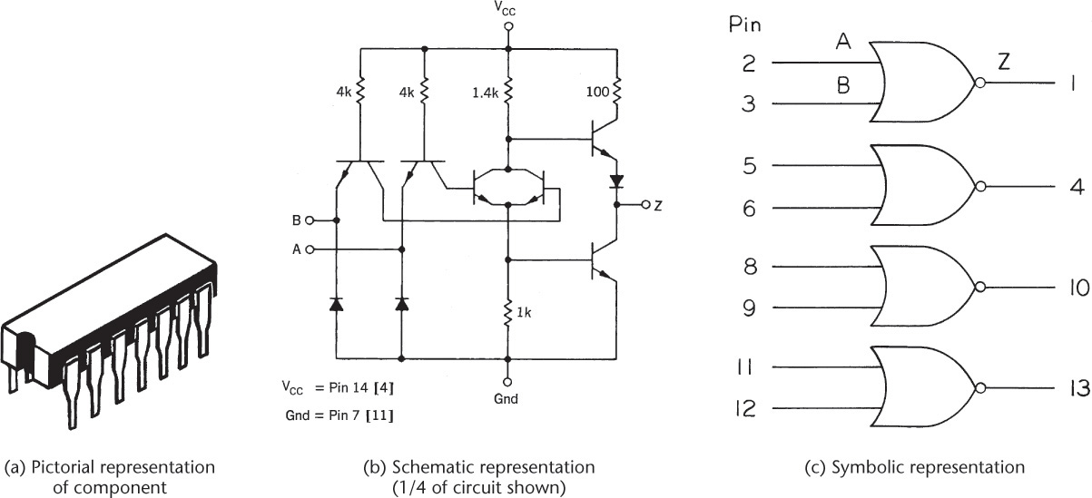
A typical integrated circuit, housed in a DIP (dual in-line package) less than an inch in length (Figure 17.34a), contains circuitry replacing all the discrete components shown in Figure 17.34b. To simplify the representation of the circuitry, use a schematic symbol, as shown in Figure 17.34c.
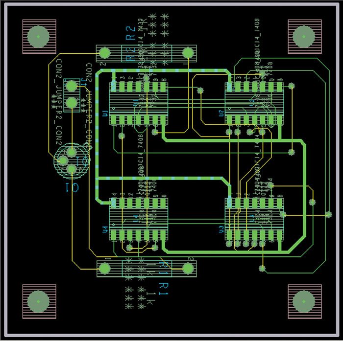
17.17 Printed Circuits
In the interests of miniaturization and mass production, printed circuit (PC) boards are widely used in the electronics industry, replacing expensive and tedious hand-wiring manufacturing methods (see Figure 17.35).
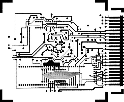
17.35 Printed Circuit Pattern (Lamit, G. Louis; Lloyd, J. Sandra, Drafting for Electronics, 3rd Ed., ©1998. Reprinted and electronically reproduced by permission of Pearson Education, Inc., New York, NY.)
A variety of procedures have been developed for fabricating these boards. Their name is derived from an early method of production, depositing (printing) a pattern of conductive ink on a base of insulating material. The method now most commonly used consists of etching a wiring pattern on copper-coated phenolic, glass–polyester, or glass–epoxy material.
Single-sided PC boards have a component side and a foil side. The component side often has part designations silk-screened on the board; on the foil side, the component leads are soldered onto the copper foil.
If CAD is not being used, once the electronic designer has decided on the physical arrangement of components to be mounted on the printed circuit board, a freehand layout sketch is made.
It is important to maintain close tolerances in the production of PC artwork, so that the various electronic components’ leads will fit properly in the spaces provided for them on the finished board. CAD circuit design software should be utilized whenever possible to provide optimum PC board designs with minimal effort.
17.18 Computer Graphics
CAD greatly simplifies the process of producing printed circuit artwork. Sophisticated programs let you reduce the physical size of the board and minimize the need for crossover jumper wires.
Double-sided printed circuit boards are common, and many compact designs require multilayer boards, in which the conductive paths are sandwiched between insulating layers. These board layouts (Figure 17.36) require precise registration of the artwork for each layer to ensure proper alignment of corresponding features, such as holes that are to be “plated through” from side to side.
17.36 The OrCAD Software’s PCB Editor Supports Autorouting of Board Components (Courtesy of Cadence® Design Systems, Inc. OrCAD® is a registered trademark of Cadence Design Systems, Inc.)
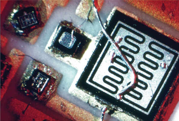
A CAD component layout program allows you to create the best possible parts placement in the shortest possible time. Microminiature surface-mount components, which have short solder tab connections instead of wire leads and so do not require drilled mounting holes, are used with increasing frequency. The small size of these parts requires a high degree of accuracy in board layout and design that CAD systems can easily provide.
CAD systems are capable of providing full-size or scaled artwork along with other data required to set up automated soldering and drilling equipment required to produce a finished printed circuit board.
Schematic Diagram or Circuit Diagram
Chapter Summary
• Schematic diagrams show the signal path between discrete components.
• Wiring diagrams show point-to-point wiring connections.
• Block diagrams show simplified representations of subsystems. Each subsystem is designated by a separate rectangular box.
• Unique graphic symbols are assigned to every electronic component. CAD programs store these symbols in a library. Schematic sketches can be created using plastic template guides.
• Computer graphics programs can automate much of the drawing needed to generate a printed circuit board layout.
• Letters and numbers are placed next to components to indicate connection points, terminal pin designations, and reference values.
Review Questions
1. In what direction does the signal path flow in a schematic diagram?
2. What is the difference between a block diagram and a schematic diagram?
3. What does each box represent in a block diagram?
4. In a schematic diagram, what does a large dot mean when two lines cross?
5. How are a component’s terminal pins identified in a schematic diagram?
6. Draw the representation of a wire that stops and then continues at a different location.
7. What type of electronic drawing shows parts in three dimensions?
8. What are the names of each side of a printed circuit board? Which side contains the soldered connections?
9. Draw the schematic symbols for 10 electronic components.
10. What is the schematic symbol for chassis ground?
Chapter Exercises
All the following problems may also be solved using CAD or freehand. If freehand sketches are assigned, 8.5″ × 11″ grid paper with .25″ grid squares is suggested. Refer to Appendix 35 for standard graphical symbols.

Exercise 17.1 The circuit shown is suitable for classroom or laboratory demonstrations. After a local radio station is tuned with a regular 9-V battery in place, other devices, such as photoelectric cells and homemade batteries, are substituted.
Make a freehand or CAD schematic diagram of the circuit, approximately twice the size of the figure. Use standard symbols and show component values and reference designations, following recommended practices.
Components List
C1 |
10-365 PF variable capacitor |
D1 |
Germanium diode |
L1 |
Loopstick antenna coil with center tap |
T1 |
Output transformer: 2500 ohm primary, |
Q1 |
NPN type RF transistor (B = base, C = collector, E = emitter) |
Q2 |
PNP type audio transistor |
Exercise 17.2 The unit shown is used to calibrate the tuning dials of shortwave communications receivers by providing a check signal every 100 kHz throughout the commonly used bands.
Reproduce the schematic diagram approximately double size, freehand or using CAD, as assigned. Add standard symbols and include reference designations, component values, and other data following recommended practices.
Components List
Capacitors |
|
C1 |
1000 PF |
C2 |
7–45 PF trimmer |
C3 |
10 PF |
Crystal |
|
Y1 |
100 kHz |
Resistors (ohms) |
|
R1 |
56K |
R2 |
56K |
Integrated Circuit |
|
U1 |
HEP 570 (quad 2-input gate) |

Exercise 17.3 The circuit shown is for a variable frequency oscillator (VFO) that may be used with transmitters operating in the 80-m amateur radio (“ham”) band.
Make a freehand or CAD schematic diagram, approximately twice the size of the figure. Use standard symbols and include reference designations and component values, following recommended practices.
Components List
Capacitors |
|
C1 |
100 PF trimmer |
C2 |
50 PF |
C3 |
150 PF variable |
C4 |
470 PF |
C5, C6 |
1000 PF |
C7, C8 |
.1 UF |
Resistors (ohms) |
|
R1, R2, R3 |
22K |
R4 |
270 |
Coils |
|
L1 |
6 UH ceramic or air core |
L2 |
1 MH RF choke |
Semiconductors |
|
D1 |
1N914 silicon diode |
D2 |
6 V, 1 W zener diode |
Q1e |
40673 dual-gate MOSFET transistor |

Exercise 17.4 Make a freehand or CAD schematic diagram of the circuit shown approximately double size. Use standard symbols and show reference designations and component values, following recommended practices.
Note: By rearranging slightly a few connecting lines, you can eliminate the three dot symbols.
Components List
Components List |
|
|
|
Capacitors |
|
Resistors (ohms) |
|
C1 |
10 PF |
R1 |
47K |
C2 |
10–365 PF variable |
R2 |
82K |
C3 |
90 UF |
R3 |
2200 |
C4 |
.005 UF |
R4 |
1000 |
C5 |
5 UF |
R5 |
10K |
C6 |
.001 UF |
R6 |
82 |
C7 |
5 UF |
R7 |
10K variable (potentiometer) |
C8 |
.01 UF |
R8 |
82K |
C9 |
.005 UF |
R9 |
5600 |
C10 |
.005 UF |
R10 |
3900 |
C11 |
90 UF |
|
|
C12 |
.005 UF |
|
|
Coils |
|
|
|
L1 |
Loopstick antenna (same symbol as magnetic core transformer) |
|
|
L2 |
Magnetic core, .5 MILLI H |
|
|
L3 |
Magnetic core, 1.0 MILLI H |
|
|
Transistors |
|
|
|
(E = emitter, B = base, C = collector) |
|
|
|
Q1 |
PNP type, RF-AF amplifier |
|
|
Q2 |
PNP type, audio amplifier |
|
|
Miscellaneous |
|
|
|
S1 |
On-off switch (mounted on R7) |
|
|
D1 |
Diode detector |
|
|
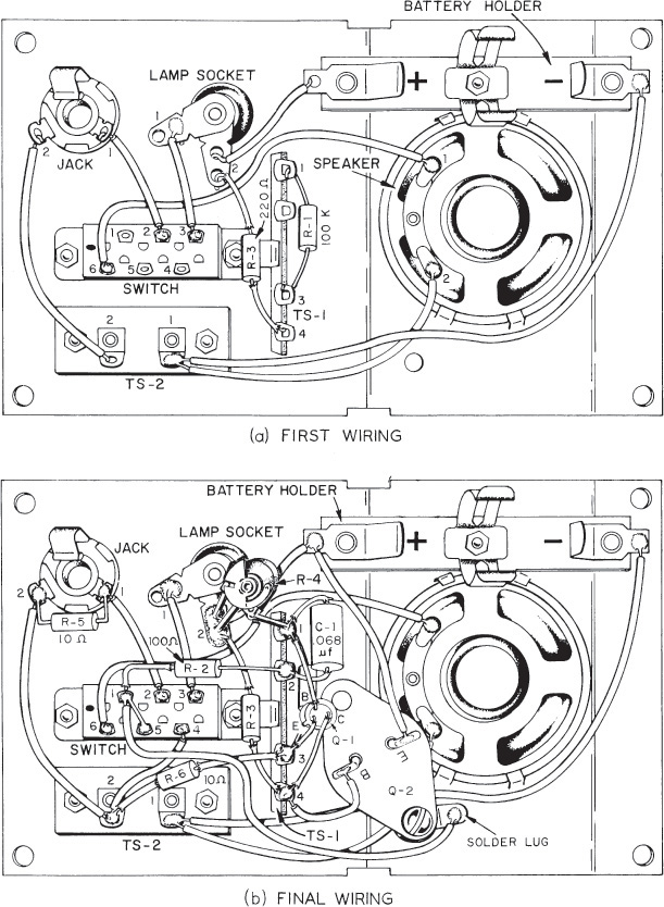
Exercise 17.5 Figures a and b are pictorial wiring diagrams of a transistorized code-practice oscillator. The unit provides for practicing International Morse Code either by listening to an audible tone over headphones or speaker or by watching a flashing light.
Study the illustrations and the components list carefully, making preliminary sketches of connections. Then, make a complete schematic diagram of the circuit following recommended practices and including component values and reference designations.
Note: Terminal strips TS-1 and TS-2 and the battery holder are for mechanical function and convenience in wiring. They should not be shown in a schematic diagram.
Components List
Capacitors |
|
C1 |
.068 UF |
Resistors (ohms) |
|
R1 |
100K |
R2 |
100 |
R3 |
220 |
R4 |
50K variable (potentiometer) |
R5 |
10 |
R6 |
10 |
Transistors |
|
(E = emitter, B = base, C = collector) |
|
Q1 |
NPN type, oscillator |
Q2 |
PNP type, amplifier |
Miscellaneous |
|
Battery |
“C” Type, 1.5 V |
Battery holder |
|
Jack |
2-conductor (for headphones) |
Key |
Telegraph key (not shown— |
Lamp, 1.5 V |
|
Lamp socket |
|
Speaker |
|
Switch |
3-position slide switch |
Connections |
|
Position one (OFF-LIGHT)—terminals 1–5, 3–4 |
|
Position two (SPEAKER)—terminals 1–6, 2–4 |
|
Position three (PHONES)—terminals 2–5 |
|
Terminal strips TS-1 and TS-2 |
|