
16
Low Power Sensor Networks
16.1 Introduction
In a variety of scenarios, often the only way to fully observe or monitor a situation is through the use of sensors. Sensors have been used in both civil and military applications, in order to extend the field of view of the end-user. However, most current sensing systems consist of a few large macrosensors, which while being highly accurate are expensive. Macrosensor systems are highly sensitive; the entire system can break down even with one faulty sensor. Trends in sensing applications are shifting towards designing networks of wireless microsensor nodes for reasons such as lower cost, ease of deployment and fault tolerance. Networked microsensors have also enabled a variety of new applications, such as environment monitoring [1], security, battlefield surveillance [2], and medical monitoring. Figure 16.1 shows an example wireless sensor network.

Figure 16.1. Microprocessor networks can be used for remote sensing
Another challenge in wireless microsensor systems is that all nodes are energy-constrained. As the number of sensors increases, it becomes infeasible to recharge all of the batteries of the individual sensors. In order to prolong the lifetimes of the wireless sensors, all aspects of the sensor system should be energy-efficient. This includes the sensor, data conversion, Digital Signal Processor (DSP), network protocols and RF communication. One important low power design consideration is leakage reduction. In sensing applications, often the sensors are idle and waiting for an external event. In such low duty cycle systems, more time is spent in idle mode than active mode, and leakage currents can become large. Therefore, circuit techniques for leakage reduction should be considered.
There are many important differences between the wireless microsensor systems discussed here and their wireless macrosensor system counterparts, that lead to new challenges in low power design [3]. In typical microsensor applications, the number of microsensors will be large which leads to high sensor node densities. As a result, the amount of sensing data will be tremendous, and it will be increasingly difficult to store and process the data. A network protocol layer and signal processing algorithms are needed to extract the important information from the sensor data. Also, the transmission distance between sensors tend to be short (<10 m) as compared to conventional macrosensors. This leads to lower transmission power being dissipated, and different architectures for computation partitioning will be necessary.
Another important design consideration in microsensors is power awareness, where all sensors are able to adapt energy consumption as energy resources of the system diminish or as performance requirements change. A power-aware node will have a longer lifetime and lend to more efficient sensor systems. Power-aware design is different than low power design, which often assumes a worst case power dissipation [4]. Instead, in power-aware design, the idea is that the system energy consumption should scale with changing conditions and quality requirements. This is important in order to enable the user to trade-off system performance parameters as opposed to hard-wiring them. For example, the user may want to sacrifice system performance or latency in return for maximizing battery lifetime. One property of a well-designed power-aware system, is one that degrades its quality and performance as available energy resources are depleted instead of exhibiting an “all-or-none” behavior. In this chapter, we discuss desirable traits of energy-quality scalable implementation of algorithms.
The application of this chapter involves use of acoustic sensors to make valuable inferences about the environment. Acoustic sensors are highly versatile and can be used in a variety of applications, such as speech recognition, traffic monitoring, and medical diagnosis. An example application is source tracking and localization. Multiple sensors can be used to pinpoint the location of an acoustic source (e.g. vehicle, speaker), by using a line of bearing estimation technique. Another example application is source classification and identification. For example, in a speech application, the end-user may want to gather speech data which can be used for speaker identification and verification. We will explore the networking, algorithmic and architectural challenges of designing wireless sensor networks in the context of these applications.
16.2 Power-Aware Node Architecture
A prototype sensor node based on the StrongARM SA-1100 microprocessor has been developed as part of the MIT micro-Adaptive Multi-domain Power-Aware Sensors (μAMPS) project. In order to demonstrate power-aware DSPs for sensor network applications, networking protocols and algorithms have been implemented and run on the SA-1100.
Figure 16.2 is a block diagram of the sensor node architecture. The node can be separated into four subsystems. The interface to the environment is through the sensing subsystem which for our node consists of two sensors (acoustic and seismic), connected to an Analog-to-Digital (A/D) converter. The acoustic sensor which is primarily used for source tracking and classification is an electret microphone with low-noise biasing and amplification. The seismic sensor is not used for this application, but is also useful for data gathering. For source tracking, a 1-kHz conversion rate of the 12-bit A/D is required. The data is continuously sampled, and stored in on-board RAM to be processed by the data and control processing subsystem.

Figure 16.2. The architectural overview of a sensor node
Depending on the role of the sensor within the network, the data is processed in the data and control processing subsystem. For example, if the sensor is a data-aggregator, then signal processing is performed. However, if the node is a relay, then the data is routed to the communication subsystem to be transmitted. The central component of the data and control processing subsystem is the StrongARM SA-1100 microprocessor. The SA-1100 is selected for its low power consumption, sufficient performance for signal processing algorithms, and static CMOS design. In addition the SA-1100 can be programmed to run at a range of clock speeds from 50 to 206 MHz and at voltage supplies from 0.8 to 1.44 V [5]. On-board ROM and RAM are included for storage of sampled data, signal processing algorithms and the “m-OS”. The μ-OS is a lightweight, multithreaded operating system constructed to demonstrate the power-aware algorithms. Figure 16.3 shows a printed circuit board which implements the StrongARM based data and control processing subsystem.
In order to collaborate with neighboring sensors and with the end-user, the data from the StrongARM is passed to the radio or communication subsystem of the node. The primary component of the radio is a commercial single-chip transceiver optimized for ISM 2.45 GHz wireless systems. The PLL, transmitter chain, and receiver chain are capable of being shut-off under software or hardware control for energy savings. To transmit data, an external Voltage-Controlled Oscillator (VCO) is directly modulated, providing simplicity at the circuit level and reduced power consumption at the expense of limits on the amount of data that can be transmitted continuously. The radio module is capable of transmitting up to 1 Mbps at a range of up to 10 m.

Figure 16.3. Printed circuit board of the data and control processing subsystem of the μAMPS sensor node
The final subsystem of the node is the battery subsystem. The power for the node is supplied by a single 3.6-V DC source, which can be provided by a single lithium-ion cell or three NiCD or NiMH cells. Regulators generate 5-, 3.3-, and adjustable 0.9–1.5-V supplies from the battery. The 5-V supply powers the analog sensor circuitry and A/D converter. The 3.3-V supply powers all digital components on the sensor node with the exception of the processor core. The core is powered by a digitally adjustable switching regulator that can provide 0.9–1.6-V in 20 discrete increments. The digitally adjustable voltage allows the SA-1100 to control its own core voltage enabling Dynamic Voltage Scaling (DVS) techniques.
16.3 Hardware Design Issues
It is important to accurately estimate the energy requirements of the hardware, so that the sensors are able to estimate the energy requirement of an application, make decisions about their processing ability based on user-input and sustainable battery life, and configure themselves to meet the required goals. For example, based on the energy model for the application and the system lifetime requirements, the sensor node should be able to decide whether a particular application can be run. If not, the node might reduce its voltage using an embedded DC/DC converter and run the application at reduced throughput or run at the same throughput but with reduced accuracy. Both of these configurations would reduce energy dissipation and increase the node's lifetime. These energy–accuracy–throughput trade-offs necessitate robust energy models for software based on parameters such as operating frequency, voltage and target processor.
16.3.1 Processor Energy Model
The computation or signal processing needed will be performed by the SA-1100 in the software. We have developed a simple energy model for software using frequency and supply voltage as parameters that incorporates explicit characterization of both switching and leakage energy. Most current models only consider switching energy [6], but in microsensor nodes which have low duty cycles, leakage energy dissipation can become large.

where CL is the average capacitance switched per cycle and N is the number of cycles the program takes to execute. Both these parameters can be obtained from the energy consumption data for a particular supply voltage, Vdd, and frequency, f, combination. The model can then be used to predict energy consumption for different supply–throughput configurations in energy-constrained environments, such as wireless microsensor networks.
Experiments on the StrongARM SA-1100 have verified this model. For the SA-1100, the processor-dependent parameters I0 and n are computed to be 1.196 mA and 21.26 mA, respectively [7]. Then at Vdd = 1.5 V and f = 206 MHz, for several typical sensor DSP routines, CL is calculated from Equation (1), and Etot is measured from the StrongARM. This CL is used with our processor energy model to estimate Etot for all possible Vdd,fcombinations. Table 16.1 shows that the maximum error produced by the model was less than 5% for a set of benchmark programs.
A more advanced level of processor energy modeling is to profile the energy for different instructions. It is natural that for different instructions the processor will dissipate different amounts of energy. Figure 16.4 shows the average current drawn from the StrongARM SA-1100 while executing different instructions at Vdd = 1.5 V. This figure shows that there are variations in current drawn for different classes of instructions (e.g. memory access, ALU), but the differences are not appreciable. Thus, the common overheads associated with all instructions (e.g. instruction fetch, caches) dominate the energy dissipated per operation. We expect that the variation between instructions will be more prominent in processors that use clock gating. Clock gating is a widely used low power technique where the clock is only enabled for those circuits that are active. Disabling non-active circuits eliminates unnecessary switching, which leads to energy savings.
Table 16.1 Software energy model performance
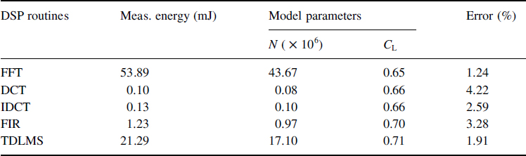
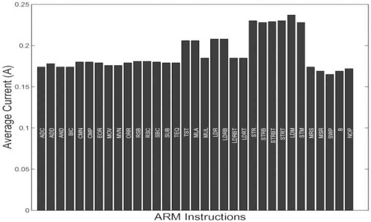
Figure 16.4. Current profiling of different instructions executed on the StrongARM SA-1100
16.3.2 DVS
Most systems are designed for the worst case scenario. For example, timing is often based on the worst case latency. For energy-scalable systems, where there is a variable computational load, this may not be optimal for energy dissipation. For example, assume in a fixed throughput system, the computation with the worst case latency takes T seconds to compute. Suppose that profiling done on the application shows that most of the time the processor is executing a task which has a computational load half that of the worst case, as shown in Figure 16.5. Since in this case, the number of cycles is halved, so the energy of a system which has fixed voltage supply will have energy savings of 1/2 over the worst case scenario. However, this is not optimal, because after the processor completes the task, it will idle for T/2 seconds. A better idea is to reduce the clock frequency by half, so that the processor is active for the entire period, and allows us to reduce the voltage supply by 1/2. According to the processor energy model (Equation (1)) the energy is linearly related to N, the number of cycles of a program and is also related to voltage supply squared. This means that by using a variable voltage supply the amount of energy dissipated is 1/4 that of the fixed voltage supply case. Figure 16.5 also shows a graph comparing Efixed and Evar for a variable workload. This graph shows the quadratic relationship between energy and computation when using a variable voltage scheme.

Figure 16.5. As processor workload varies, using a variable power supply gives quadratic savings
Figure 16.6a depicts the measured energy consumption of an SA-1100 processor running at full utilization. Energy consumed per operation is plotted with respect to the processor frequency and voltage. This figure shows the quadratic dependence of switching energy on supply voltage, and also for a fixed voltage, the leakage per operation increases as the operations occur over a longer clock period. Figure 16.6b shows all 11 frequency-voltage pairs for the StrongARM SA-1100. DVS is a technique which changes the voltage supply and clock frequency of a processor depending on the computational load. It is one technique which enables energy-scalability, as it allows the sensor to change its voltage supply depending on changing requirements. Figure 16.7 illustrates the regulation scheme on our sensor node for DVS support. The μOS running on the SA-1100 selects one of the above 11 frequency–voltage pairs in response to the current and predicted workload. A 5-bit value corresponding to the desired voltage is sent to the regulator controller, and logic external to the SA-1100 protects the core from a voltage that exceeds its maximum rating. The regulator controller typically drives the new voltage on the buck regulator in under 100 ms. At the same time, the new clock frequency is programmed into the SA-1100, causing the on-board PLL to lock to the new frequency. Relocking the PLL requires 150 ms, and computation stops during this period.

Figure 16.6. (a) Measured energy consumption characteristics of SA-1100. (b) Operating voltage and frequency pairs of the SA-1100

Figure 16.7. Feedback for dynamic voltage scaling
16.3.3 Leakage Considerations
Processor leakage is also an important consideration that can impact the policies used in the network. With increasing trends towards low power design, supply voltages are constantly being lowered as an effective way to reduce power consumption. However, to satisfy the ever demanding performance requirements, the threshold voltage is also scaled proportionately to provide sufficient current drive and reduce the propagation delay. As the threshold voltage is lowered, the subthreshold leakage current becomes increasingly dominant.
We can measure the leakage current from the slope of the energy characteristics, for constant voltage operation. One way to look at the energy consumption is to measure the amount of charge that flows across a given potential. The charge attributed to the switched capacitance should be independent of the execution time, for a given operating voltage, while the leakage charge should increase linearly with the execution time. Figure 16.8a shows the measured charge flow as a function of the execution time for a 1024-point Fast-Fourier Transform (FFT). The amount of charge flow is simply the product of the execution time and current drawn. As expected, the total charge consumption increases almost linearly with execution time and the slope of the curve, at a given voltage, directly gives the leakage current at that voltage. The leakage current at different operating voltages was measured as described earlier, and is plotted in Figure 16.8b. These measurements verified the following model for the overall leakage current for the microprocessor core

Figure 16.8. (a) The charge consumption for 1024-point FFT. (b) The leakage current as a function of supply voltage
![]()
where I0 = 1.196 mA and n = 21.26 for the StrongARM SA-1100.
Figure 16.9 shows the results after running simulations of the FFT algorithm on the StrongARM SA-1100 to demonstrate the relationship between switching and leakage energy dissipated by the processor. The leakage energy rises exponentially with supply voltage and decreases linearly with increasing frequency. Therefore to reduce energy dissipation, leakage effects must be addressed in low power design of the sensor node.

Figure 16.9. Leakage energy dissipation can be larger than switching energy dissipation
Figure 16.10 shows current consumption trends in microprocessors for low power applications based on the ITRS report [8]. Process technology scaling improves switching speed of CMOS circuits and increases the number of transistors in a chip. To suppress a rapid increase in current consumption, the power supply is also reduced. Therefore, processor operating current increases slightly as shown in Figure 16.10i. The device threshold is reduced to maintain the switching speed at reduced power supply values. As a result, subthreshold-leakage current grows larger with technology scaling as shown in Figure 16.10ii. Thus, the operating current of the processor is strongly affected by the leakage current in advanced technologies. Using leakage control methods can significantly reduce the subthreshold leakage current in idle mode as shown in Figure 16.10iii.

Figure 16.10. Current consumption trend in microprocessors for portable applications
There are various ways to control the leakage. One approach is to use a high threshold voltage (Vth) MOS transistor as a supply switch to cut-off leakage during idle mode. It is represented by the Multiple Threshold-voltage CMOS (MT-CMOS) scheme [9]. Another approach to control leakage involves threshold-voltage adaptation using substrate-bias (Vbb) control that is represented by the Variable Threshold-voltage CMOS (VT-CMOS) scheme [10]. A third scheme is the switched substrate-impedance scheme.
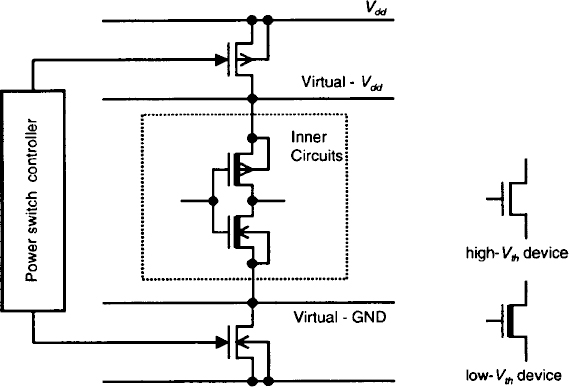
16.3.3.1 MT-CMOS
Figure 16.11 shows a diagram of the MT-CMOS scheme. MT-CMOS uses high-Vth devices as supply-source switches. Inner logic circuits are constructed from low-Vth devices. During active mode, the switches “short” power source (Vdd) and ground (GND) with virtual Vdd and virtual GND, respectively. The high-Vth devices turn off during idle mode to cut-off the leakage current of low-Vth devices.
Measurements taken from the 1-V TI DSP [11] show that leakage energy is reduced without any drop in performance. They compared a DSP fabricated entirely in high-Vth with one fabricated using MT-CMOS. At 1 V they were not able to clock the high-Vth DSP at the same clock speed as the MT-CMOS DSP, and therefore had to increase the voltage supply. This caused an increase in energy dissipation.
One drawback of using MT-CMOS is that the high-Vth supply switch produces a voltage drop between the power lines and the virtual-power lines due to the switch resistance [12]. Consequently, the drop reduces performance of the inner circuits. Therefore, the total width of the high-Vth devices must be as large as the inner circuits to reduce the voltage drop. However, large switches require a large chip area.
Another drawback is that power is not supplied to the inner circuits during idle mode and memory circuits, such as registers and caches lose their information in the idle mode. There have been some proposed circuits to hold the memory information. One solution is an intermittent power supply scheme, similar to the refresh process of DRAMs [13]. A balloon circuit is another method that is separated from the low-Vth inner devices to keep the inner circuit performance high in active state [14]. A third method is using virtual power rail clamps that set diodes between power lines and virtual power lines. The clamps supply low voltage to the inner circuits during idle state [15].
16.3.3.2 VT-CMOS
The VT-CMOS scheme changes the substrate biases (Vbb.p and Vbb.n, for pMOS-substrate and nMOS-substrate, respectively) depending on a processor's mode. A Vbb controller generates Vdd and GND during active mode, and pulls Vbb.n lower than GND and Vbb.p higher than Vdd during idle mode. In general, decreasing Vbb.n and increasing Vbb.p increases Vth, which leads to lower subthreshold leakage currents. Similar to the MT-CMOS case, there is a possibility that active operation of the circuits controlled by the VT-CMOS becomes unstable due to the Vbb noise. However, a low impedance source to the substrate does not lead to high subthreshold leakage. The width of the Vbb switches is increased to prevent Vbb noise, but they are still smaller than the Vdd switch for the MT-CMOS case.
16.3.3.3 Switched Substrate-Impedance Scheme
The switched substrate-impedance scheme [16] as shown in Figure 16.12 is one solution for reducing Vbb noise by using high-Vth transistors. This system distributes switch cells as Vbb supply switches. The switch cells turn on by signals Φp and Φn during active mode. For the inner circuits, the switches connect Vdd and GND lines with Vbb.p and Vbb.n lines, respectively. In idle mode, the high-Vth switches turn off and the substrate-switch controller supplies appropriate Vbb.p and Vbb.n.

Figure 16.12. Switched substrate-impedance scheme
There are some drawbacks to using the switched substrate-impedance scheme. One drawback occurs when the impedance of the Vbb switch is high, and the inner-circuits substrate lines are floating from power sources during the active mode. Unstable Vbbs degrade the performance of inner circuits. Another drawback is that the signals Φp and Φn have propagation delays, which cause operation errors of the inner circuits when the circuits change from idle to active mode. A feedback cell is adopted to avoid this problem.
This technique has been used in the design of the Hitachi low power microprocessor “Super-H4 (SH4)”. The SH4 has achieved 1000 MIPS/W of performance. It has several operating modes. In the active mode, the processor is fully operational and consumes 420 mA current at 1.8 V voltage supply. In sleep mode, the distributed clock signals are disabled, but the clock generators and peripheral circuits are active. The sleep mode current is 100 mA. In standby mode, all modules are suspended including the clock generators and peripherals, and also the Vbb controller is enabled. A test chip was built to measure the standby current [16]. Results show that without the switched substrate-impedance scheme enabled, the standby current is 1.3 mA. With the Vbb controller on, the standby current of the entire test chip is 46.5 μA, and the overhead due to the Vbb controller and substrate leakage is 16.5 μA. Figure 16.13 shows the test chip micrograph of the SH4 with the switched substrate-impedance scheme implemented. The SH4 contains approximately 4M transistors, and the switch cells added for leakage reduction totaled 10K transistors. A uniform layout of one Vbb switch every 100 standard cells is employed. In an SRAM, the switches are set along with the word line, and in the data path, they are lined in vertical direction to the data flow. Such a distribution method guarantees the stable and high-speed inner-circuit operation. The substrate-switch controller transistor occupies 0.3% of the chip. The area overhead of the scheme is less than 5%.

Figure 16.13. Chip micrograph adapting switched substrate-impedance scheme
16.4 Signal Processing in the Network
As the number of sensors grows larger and larger, it becomes difficult to store and process the data collected from the sensors. Also node densities increase, so that multiple sensors may view the same event. To reduce energy dissipation, the sensors should collaborate with each other, should reduce communicating redundant information and should extract the important information from the sensor data. This is done by having a network protocol layer in order for sensors to communicate locally. Data aggregation should done on highly correlated data to reduce redundancies. By providing hooks to trade-off between computational energy and communication energy, the sensor nodes can be more energy efficient. Commercial radios typically dissipate ~150 nJ/bit and the StrongARM dissipates 1 nJ/bit [17]. In a custom DSP, the energy dissipated can be as low as 1 pJ/bit. Therefore since communication is cheap, it is more energy efficient if we can reduce the amount of data transmitted, by first doing data aggregation. Finally signal processing algorithms are used to make important inferences from the data. This section discusses optimizing protocols for microsensor networks such that signal processing is done locally at the sensor node. We also discuss optimal partitioning of computation among multiple sensors for further energy savings.
16.4.1 Optimizing Protocols
Often, sensor networks are used to monitor remote areas or disaster situations. In both of these scenarios, the end-user cannot be located near the sensors. Thus, direct communication between the sensors and the end-user, as shown in Figure 16.14a, is extremely energyintensive, since transmission energy scales as rn (n typically 2–4 [18]). In addition, since direct communication does not enable spatial re-use, this approach may not be feasible for large-scale sensor networks. Thus new methods of communication need to be developed.
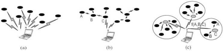
Figure 16.14. (a) Direct communication with basestation. (b) Multi-hop communication with basestation. (c) Clustering algorithm. The grey nodes represent “clusterheads”, and the function f(A,B,C) represents the data fusion algorithm
A common method of communication in wireless networks is multi-hop routing, where sensors act as routers for other sensors' data in addition to sensing the environment, as shown in Figure 16.14b [19–21]. Multi-hop routing minimizes the distance an individual sensor must transmit its data, and hence minimizes the dissipated energy for that sensor. One method of choosing routes is to minimize the total amount of transmit power necessary to get data from the node to the base station. In this case, the intermediate nodes are chosen such that the transmit amplifier energy (e.g. ETx-amp(k,d) = ![]() amp × k × d2) is minimized. For example, as shown in Figure 16.14b, node A would transmit to node C through node B if
amp × k × d2) is minimized. For example, as shown in Figure 16.14b, node A would transmit to node C through node B if
![]()
or
![]()
However, multi-hop routing requires that several sensors transmit and receive a particular signal, so this protocol may not achieve global energy efficiency. In addition, the sensors near the end-user will be used as routers for a large number of the other sensors, and their lifetimes will be dramatically reduced using such a multi-hop protocol.
Since data from neighboring sensors will often be highly correlated, it is possible to aggregate the data locally using an algorithm such as beamforming and then send the aggregate signal to the end-user to save energy. Algorithms which can be used for data aggregation include the maximum power beamforming algorithm [22] and the Least Mean Square (LMS) beamforming algorithm [23]. These algorithms can extract the common signal from multiple sensor data.
Figure 16.15 shows the amount of energy required to aggregate data from two, three, and four sensors and to transmit the result to the end-user (Elocal), as compared to all of the individual sensors transmitting data to the end-user (Ebasestation). As shown in this plot, there is a large advantage to using local data aggregation (LMS beamforming algorithm), rather than direct communication when the distance to the basestation is large.
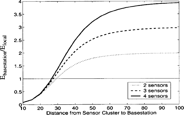
Figure 16.15. Data aggregation done locally can reduce energy dissipation
Clustering protocols that utilize the energy savings from data aggregation can greatly reduce the energy dissipation in a sensor system. Using Low Energy Adaptive Clustering Hierarchy (LEACH) [24], an energy-efficient clustering protocol, the sensors are organized into local clusters, as shown in Figure 16.14c. Each cluster has a “clusterhead”, a sensor that receives data from all other sensors in the cluster, performs data fusion (e.g. beamforming), and transmits the aggregate data to the end-user. This greatly reduces the amount of data that is sent to the end-user and thus achieves energy efficiency. Furthermore, the clusters can be organized hierarchically such that the clusterheads transmit the aggregate data using a multi-hop approach, rather than directly to the end-user so as to further reduce energy dissipation.
16.4.2 Energy-Efficient System Partitioning
One way to improve energy efficiency is to design algorithms which take advantage of the dense localization of nodes in the network. As discussed in Section 16.4.1, closely located sensors have highly correlated data that can be used in signal processing algorithms to reduce communication costs. Another way to reduce energy dissipation is to distribute the computation among the sensors. One application which demonstrates distributed processing is vehicle tracking using acoustic sensors. In this section we present an algorithm that can be performed in a distributed fashion to find the location of the vehicle.
Suppose a vehicle is moving over a region where a network of acoustic sensing nodes has been deployed. In order to determine the location of the vehicle, we first need to find the Line of Bearing (LOB) or direction from which sound is being detected. Using a LOB estimation algorithm, localization of the source can be easily accomplished. Multiple arrays or clusters of sensors determine the source's LOB from their perspective and the intersection of the LOBs determines the source's location. Figure 16.16 shows the scenario for vehicle tracking using LOB estimation.
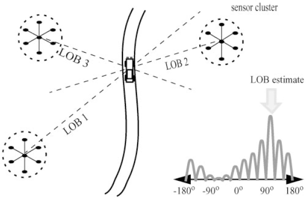
Figure 16.16. LOB estimation to do vehicle tracking
To do tracking using LOB estimates, a clustering protocol is assumed. First within a cluster individual sensors send their acoustic data to the clusterhead. Multiple clusters determine the source's LOB to be the direction with maximum sound energy from their perspective. At the basestation the intersection point of multiple LOBs will determine the source's location.
To perform LOB estimation, one can use frequency-domain beamforming [25]. Beamforming is the act of summing the outputs of filtered sensor inputs. In a simple delay-and-sum beamformer, the filtering operations are delays or in the frequency domain phase shifts. The first part of frequency-domain beamforming is to transform collected acoustic sensor data from each sensor into the frequency domain using a 1024-point FFT. Then, we beamform the FFT data into 12 uniform directions to produce 12 candidate signals. The direction of the signal with the most energy is the LOB of the source. Figure 16.17 is a block diagram of the LOB algorithm.
The LOB estimation algorithm can also be implemented in two different ways. In the direct technique, each sensor i has a set of acoustic data si(n). This data is transmitted to the clusterhead where the FFT and beamforming are performed. This technique is demonstrated in Figure 16.18a. Alternatively we can first perform the FFTs at each sensor and then send the FFT results to the clusterhead. This method is called the distributed technique and is demonstrated in Figure 16.18b. If we assume the radio and processor models discussed previously, then performing the FFTs with the distributed technique has no energy advantage over the direct technique. This is because performing the FFTs at the sensor node does not reduce the amount of data that needs to be transmitted. Thus the communication costs remain the same. However, by adding circuitry to perform Dynamic Voltage Scaling (DVS), the node can take advantage of the parallelized computation load by allowing voltage and frequency to be scaled while still meeting latency constraints.
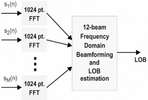
Figure 16.17. Block diagram of the LOB estimation algorithm
For example, if computation, C, can be computed using two parallel functional units instead of one, then the throughput is increased by 2. However if the latency is fixed, by instead using a clock frequency of f/2, and voltage supply of Vdd/2, then the energy is reduced by 4 times over the non-parallel case. Equation (1) demonstrates that by reducing Vdd yields quadratic savings in energy, but at the expense of additional propagation delay through static logic.
In the DVS enabled sensor node, there is a large advantage to having the computation distributed among the sensor nodes, since the voltage supply can be reduced. Table 16.2 shows the energy results for a seven-sensor cluster. In the direct technique, with a computation latency constraint of 20 ms, all of the computation is performed at the clusterhead at the fastest clock speed, f = 206 MHz at 1.44 V. The energy of the computation is 6.2 mJ and the latency is 19.2 ms. In the distributed technique, the FFT is parallelized to the sensor nodes. In this scheme, the sensor nodes sense data and perform the 1024-point FFTs on the data before transmitting the FFT data to the clusterhead. At the clusterhead, the beamforming and LOB estimation is done. Since the FFTs are parallelized, the clock speed and voltage supply of both the FFTs and the beamforming can be lowered. For example, if the FFTs at the sensor nodes are run at 0.85 V and 74 MHz clock speed while the beamforming algorithm is run at 1.17 V and 162 MHz clock speed then with a latency of 18.4 ms, only 3.4 mJ is dissipated. This is a 45.2% improvement in energy dissipation. This example shows that energy-efficient system partitioning by parallelism in system design can yield large energy savings.

Figure 16.18. (a) Direct technique: all of the computation is done at the clusterhead. (b) Distributed technique: distribute the FFT computation among all sensors
Table 16.2 Energy results for direct and distributed techniques for a seven-sensor cluster
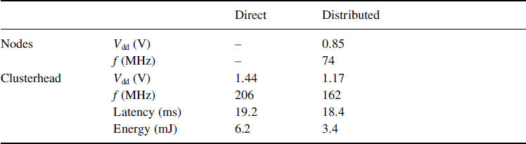
Figure 16.19 compares the energy dissipated for the direct techniques versus that for the distributed technique as the number of sensors is increased from three to ten sensors. This plot shows that a 20–50% energy reduction can be achieved with the system partitioning scheme.

Figure 16.19. Comparing computation energy dissipated for the direct technique vs. the distributed technique
Therefore it is important to have efficient system partitioning of computation considerations when designing protocols for wireless sensor networks.
16.5 Signal Processing Algorithms
Energy scalability can be achieved by monitoring energy resources, latency and performance requirements to dynamically reconfigure system functionality [25]. Energy–Quality (E–Q) trade-offs have been explored in the context of encryption processors [26]. Energy scalability at the algorithm and protocol levels is highly desirable because a large range of both energy and quality can be achieved by varying algorithm parameters. A large class of algorithms, as they stand, do not render themselves to such E–Q scaling.
Let us assume that there exists a quality distribution pQ(x), the probability that the end-user desires quality x. Then the average energy consumption per output sample can then be expressed as
![]()
where ![]() (x) is the energy dissipated by the system to give quality x. A typical E–Q distribution is shown in Figure 16.20. It is clear that Algorithm II is desirable over Algorithm I because it gives higher quality at lower energies and especially when pQ(x) is large.
(x) is the energy dissipated by the system to give quality x. A typical E–Q distribution is shown in Figure 16.20. It is clear that Algorithm II is desirable over Algorithm I because it gives higher quality at lower energies and especially when pQ(x) is large.
When the quality distribution is unknown, the E–Q behavior of the algorithm can be engineered such that it has two desirable traits. First, the quality on average should be monotonically increasing as energy increases and second, the E–Q curve should be concave downward
![]()
![]()

Figure 16.20. Examples of E–Q curves
where Q(E) is an accurate model of the algorithm's average quality as a function of computational energy and is the inverse of E(Q). These constraints lead to intelligent energy-scalable systems. An E–Q curve that is concave downward is highly desirable since close to maximal quality is achieved at lower energies. Conversely, a system that has a concave upward E–Q curve can only guarantee high quality by expending a large amount of energy.
Algorithmic transformations can be used to improve the E–Q characteristics of a system. For example, we will show that the E–Q curves for both Finite Impulse Response (FIR) filtering and LMS beamforming for data aggregation can be transformed for better energy scalability systems.
16.5.1 Energy–Agile Filtering
FIR filtering is one of the most commonly used DSP operations. FIR filtering involves the inner product of two vectors one of which is fixed and known as the impulse response, h[n], of the filter [27]. An N-tap FIR filter is defined by Equation (8).

However, when we analyze the FIR filtering operation from a pure inner product perspective, it simply involves N Multiply and Accumulate (MAC) cycles. For desired E–Q behavior, the MAC cycles that contribute most significantly to the output y[n] should be done first. Each of the partial sums, x[k]h[n – k], depends on the data sample and therefore it is not apparent which ones should be accumulated first. Intuitively, the partial sums that are maximum in magnitude (and can therefore affect the final result significantly) should be accumulated first. Most FIR filter coefficients have a few coefficients that are large in magnitude and progressively reduce in amplitude. Therefore, a simple but effective most-significant-first transform involves sorting the impulse response in decreasing order of magnitude and reordering the MACs such that the partial sum corresponding to the largest coefficient is accumulated first as shown in Figure 16.21a. Undoubtedly, the data sample multiplied to the coefficient might be so small as to mitigate the effect of the partial sum. Nevertheless, on an average case, the coefficient reordering by magnitude yields a better E–Q performance than the original scheme.
Figure 16.21b illustrates the scalability results for a low pass filtering of speech data sampled at 10 kHz using a 128-tap FIR filter whose impulse response (magnitude) is also outlined. The average energy consumption per output sample (measured on the StrongARM SA-1100 operating at 1.44 V power supply and 206 MHz frequency) in the original scheme is 5.12 mJ. Since the initial coefficients are not the ones with most significant magnitudes the E–Q behavior is poor. Sorting the coefficients and using a level of indirection (in software that amounts to having an index array of the same size as the coefficient array), the E–Q behavior can be substantially improved. It can be seen that fluctuations in data can lead to deviations from the ideal behavior suggested by Equation (7), nonetheless overall concavity is still apparent. The energy overhead associated with using a level of indirection on the SA-1100 was only 0.21 mJ which is about 4% of the total energy consumption.
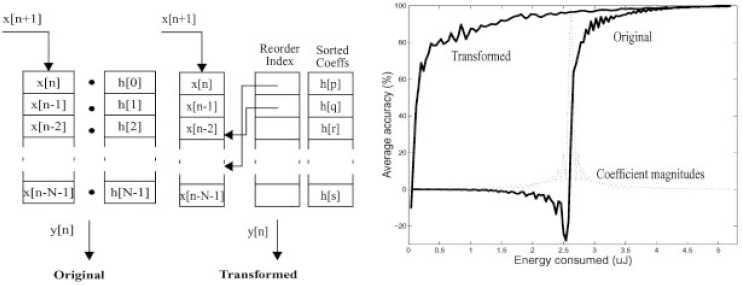
Figure 16.21. (a) FIR filtering with coefficient reordering. (b) E–Q graph for original and transformed FIR filtering
16.5.2 Energy–Agile Data Aggregation
The most-significant-first transform can also be used to improve the E–Q curves for LMS beamforming of sensor data as shown in our testbed in Figure 16.22. In order to determine the E–Q curve of the LMS beamforming algorithm, we perform beamforming on the sensor data, measure the energy dissipated on the StrongARM, and calculate the matched filter (quality) output as we vary the number of sensors in beamforming and as the source moves from location A to B. In Scenario 1, we perform beamforming without any knowledge of the source location in relation to the sensors. Beamforming is done in a preset order ![]() 1,2,3,4,5,6
1,2,3,4,5,6![]() . The parameter we use to scale energy is k, the number of sensors in beamforming. As k is increased from 1 to 6, there is a proportional increase in energy. As the source moves from location A to B, we take snapshots of the E–Q curve, shown in Figure 16.23a. This curve shows that with a preset beamforming order, there can be vastly different E–Q curves depending on the source location. When the source is at location A, the beamforming quality is only close to maximum when k = 5,6. Conversely, when the source is at location B, the beamforming quality is close to maximum when k = 2. Therefore, since the E–Q curve is highly data dependent, desirable E–Q scalability cannot be guaranteed.
. The parameter we use to scale energy is k, the number of sensors in beamforming. As k is increased from 1 to 6, there is a proportional increase in energy. As the source moves from location A to B, we take snapshots of the E–Q curve, shown in Figure 16.23a. This curve shows that with a preset beamforming order, there can be vastly different E–Q curves depending on the source location. When the source is at location A, the beamforming quality is only close to maximum when k = 5,6. Conversely, when the source is at location B, the beamforming quality is close to maximum when k = 2. Therefore, since the E–Q curve is highly data dependent, desirable E–Q scalability cannot be guaranteed.

Figure 16.22. A testbed of sensors for vehicle classification
An intelligent alternative is to perform some initial pre-processing of the sensor data to determine the desired beamforming order for a given set of sensor data. Intuitively, we want to beamform the data from sensors that have higher sensor signal energy. We propose the most-significant-first transform, which can be applied to many algorithms to improve E–Q characteristics. To find the desired beamforming order, first the sensor signal energy is estimated from the sensor data. Then the sensor signal energies are sorted using a quicksort method. The quicksort output determines the desired beamforming order.

Figure 16.23. (a) The E–Q snapshot as the source moves from location A to B for the scenario of LMS beamforming with a pre-set order of sensor data. (b) The E–Q snapshot as the source moves from location A to B for the scenario of LMS beamforming with significance ordering of sensor data.
Figure 16.23b shows the E–Q relationship when an algorithmic transform is used. In this scenario, with the most-significant-first transform, we can ensure that the E–Q graph is concave downward, thus improving the E–Q characteristics for beamforming. However, there is a price to pay in computation energy. If the energy cost required to compute the sensor signal energies and quicksort is large compared to LMS beamforming, the most significant first transform does not improve energy efficiency. For our example, the overhead computational energy was 8.8 mJ, only 0.41% the required energy for two-sensor LMS beamforming when simulated on the SA-1100.
16.6 Signal Processing Architectures
Energy-scalable architectures have been explored to implement power-aware systems. In this section, we introduce architectures for variable-length filtering and variable-precision filtering.
16.6.1 Variable-Length Filtering
The LMS beamforming algorithm block can be implemented using a tapped delay line approach as shown in Figure 16.24. Energy is scaled by powering down the latter parts of the tapped delay line, at the expense of shorter filter lengths which can affect the performance of the LMS algorithm. Increasing the length of the adaptive filter improves the frequency resolution of the signal processing done, thus reducing mean squared error (MSE) and improving performance. However, this comes at the cost of an increase in energy dissipation. In a software implementation on the SA-1100, the number of cycles increases linearly as the filter length is increased. Thus given a specified performance requirement, the latter parts of the tapped delay line can be disabled to reduce the number of processor cycles. This, in turn, reduces the energy dissipated.

Figure 16.24. The LMS beamforming algorithm can be implemented using a tapped delay line structure
A simple variable-length filter controller can determine the appropriate filter length by monitoring the (MSE)

where the error function, ε(n), is the mean squared error of the converging processes. A programmable threshold, α, is set and the filter length is set initially to the maximum length, Lmax. On a frame to frame basis, the filter length is decreased until the MSE is greater than α. Figure 16.25 shows the relationship between matched filter response (quality) and filter length. The optimal filter length is highly data dependent, but in general, a filter that is too short may not provide enough frequency resolution, but a filter that is too long takes longer to converge to the optimal solution.
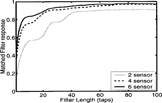
Figure 16.25. A plot of quality vs. filter length for the LMS algorithm
Measurements from the StrongARM show that a variable-length filtering scheme can be used in conjunction with DVS for further energy savings. This is shown in Figure 16.26. This plot shows that as the program latency increases which corresponds to decreasing clock frequency, there is a large amount of energy savings using a variable voltage supply over using a fixed voltage supply.
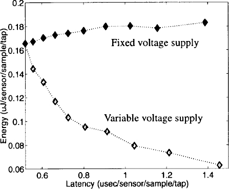
Figure 16.26. Latency vs. energy for a variable voltage supply on the StrongARM SA-1100
16.6.2 Variable Precision Architecture
When the filter coefficients in an FIR filtering scheme are fixed, the flexibility offered by a dedicated multiplier is not required. Distributed Arithmetic (DA) is a bit-serial, multiplier-less technique that exploits the fact that one of the vectors in the inner product is fixed [28]. All possible intermediate computations (for the fixed vector) are stored in a Look-up Table (LUT) and bit slices of the variable vector are used as addresses for the LUT. A four-tap DA based FIR filter is shown in Figure 16.27.
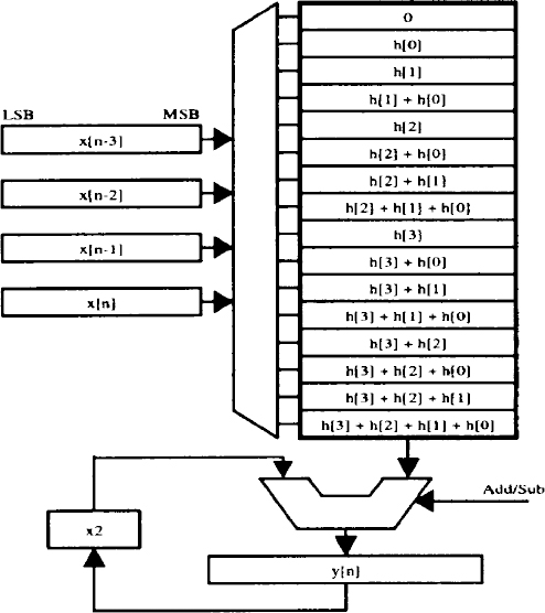
Figure 16.27. Implementation of a four-tap filter using DA
The MSB first implementation using variable precision architecture will have desirable energy–quality characteristics. By processing the MSB first, then the most significant values are processed first. In the MSB first implementation of Figure 16.27, it has been shown in [29] that each successive intermediate value is closer to the final value in a stochastic sense. Let us assume that the maximum precision requirement is Mmax and the immediate precision requirement is M ≤ Mmax. This scales down the energy per output sample by a factor M/Mmax. Lesser precision implies that the same computation can be done faster (i.e. in M cycles instead of Mmax).
DVS can also be used in conjunction with our variable precision architecture for further energy savings. By switching down the operating voltage such that we still meet the worst case throughput requirement (i.e. corresponding to one output sample every Mmax cycles when operating at Vmax), quadratic energy savings are achieved. Figure 16.28 illustrates the precision distribution for typical speech data. Notice that the distribution peaks around M = 4 which implies that a large fraction of the speech processing can be done using a DA for variable precision processing and reduced energy dissipation.
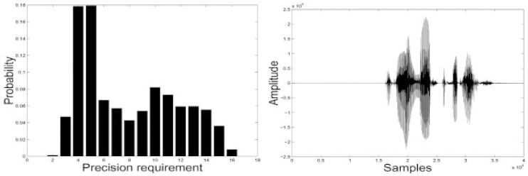
Figure 16.28. Probability distribution of precision requirement
16.7 Conclusions
In this chapter, many new design challenges have been introduced in the field of wireless microsensor networks. A great deal of signal processing will happen at the sensor node, so it is important that the sensor node have a very energy-efficient DSP. For example, the DSP should be designed with leakage reduction due to the low-duty cycle nature of the applications. Also the DSP should allow for dynamic voltage scaling, so that for variable computational loads, the voltage and clock frequency can be dynamically reduced for further energy reduction.
Other important design considerations are the networking, algorithmic and architectural aspects of the microsensor system. In this chapter, it is shown that a clustering network protocol, which allows for sensor collaboration is highly energy-efficient. Also, optimal system partitioning of computation among the sensors in a cluster is explored. Also introduced in this chapter, are ways to implement signal processing algorithms such that they have desirable energy–quality characteristics. This is verified through energy–agile filtering and energy–agile beamforming. Finally, energy-scalable architectures are presented, which enable power-aware algorithms. Two examples of energy-scalable architectures are variable filter-length architectures and variable precision distributed arithmetic units.
As technology continues to advance, one day it will become possible to have these compact, low cost wireless sensors embedded throughout the environment, in homes/offices and ultimately inside people. With continued advances in power management, these systems should find more numerous and more impressive applications. Until that day, there is a rich set of research problems associated with distributed microsensors that require very different solutions than traditional macrosensors and multimedia devices. Energy dissipation, scalability, and latency must all be considered in designing network protocols for collaboration and information sharing, system partitioning and low power electronics.
References
[1] Karn, J., Katz, R. and Pister, K., ‘Next Century Challenges: Mobile Networking for Smart Dust’, Proceedings of ACM MobiCom '99, August 1999.
[2] Asada, G., Dong, M., Lin, T.S., Newberg, F., Pottie, G. and Kaiser, W.J., ‘Wireless Integrated Network Sensors: Low Power Systems on a Chip’, Proceedings of ESSCIRC '98, 1998.
[3] Estrin, D., Govindan, R., Heidemann, J. and Kumar, S., ‘Next Century Challenges: Scalable Coordination in Sensor Networks’, Proceedings of ACM MobiCom '99, August 1999.
[4] Bhardwaj, M., Min, R. and Chandrakasan, A., ‘Power-Aware Systems’, Proceedings of the 34th Asilomar Conference on Signals, Systems, and Computers, November 2000.
[5] Advanced RISC Machines Ltd., Advance RISC Machines Architectural Reference Manual, Prentice Hall, New York, 1996.
[6] Tiwari, V. and Malik, S., ‘Power Analysis of Embedded Software: A First Approach to Software Power Minimization’, IEEE Transactions on VLSI Systems, Vol. 2, December 1994.
[7] Sinha, A. and Chandrakasan, A., ‘Energy Aware Software’, VLSI Design 2000, Calcutta, India, January 2000.
[8] http://public.itrs.net/files/1999_SIA_Roadmap/Home.htm
[9] Mutoh, S., Douseki, T., Matsuya, Y., Aoki, T. and Yamada, J., ‘1-V high-Speed Digital Circuit Technology with 0.5 μm Multi-Threshold CMOS’, Proceedings of IEEE International ASIC Conference and Exhibition, 1993, pp. 186–189.
[10] Kuroda, T., Fujita, T., Mita, S., Nagamatu, T., Yoshioka, S., Sano, F., Norishima, M., Murota, M., Kako, M., Kinugawa, M., Kakumu, M. and Sakurai, T. ‘A 0.9-V, 150-MHz, 10-mW, 4-mm 2D Discrete Cosine Transform Core Processor with Variable-Threshold-Voltage Scheme’ , ISSCC Digest of Technical Papers, 1996, pp. 166–167.
[11] Lee, W., Landman, P.E., Barton, B., Abiko, S., Takahashi, H., Mizuno, H., Muramatsu, S., Tashiro, K., Fusumada, M., Pham, L., Boutaud, F., Ego, E., Gallo, G., Tran, H., Lemonds, C., Shih, A., Nandakumar, M., Eklun, R.H. and Chen, I.C., ‘1-V Programmable DSP for Wireless Communications’, IEEE Journal of Solid-State Circuits, Vol. 32, No. 11, November 1997.
[12] Mutoh, S., Douseki, T., Matsuya, Y., Aoki, T., Shigematsu, S. and Yamada, J., ‘1-V power supply high-speed digital circuit technology with multithreshold-voltage CMOS’, IEEE Journal of Solid-State Circuits, Vol. 30, No. 8, August 1995, pp. 847–854.
[13] Akamatsu, H., Iwata, T., Yamamoto, H., Hirata, T., Yamauchi, H., Kotani, H. and Matsuzawa, A., ‘A Low Power Data Holding Circuit with an Intermittent Power Supply Scheme for Sub-1-V MT-CMOS LSIs’ , Symposium on VLSI Circuits Digest of Technical Papers, 1996, pp. 14–15.
[14] Shigematsu, S., Mutoh, S., Matsuya, Y., Tanabe, Y. and Yamada, J., ‘A 1-V High-Speed MTCMOS Circuit Scheme for Power-Down Application Circuits’, IEEE Journal of Solid-State Circuits, Vol. 32, No. 6, 1997, pp. 861–869.
[15] Kumagai, K., Iwaki. H., Yoshida, H., Suzuki, H., Yamada, T. and Kurosawa, S., ‘A Novel Powering-Down Scheme for Low Vt CMOS Circuits’, Symposium on VLSI Circuits Digest of Technical Papers, 1998, pp. 44–45.
[16] Mizuno, H., Ishibashi, K., Shimura, T., Hattori, T., Narita, S., Shiozawa, K., Ikeda, S. and Uchiyama, K., ‘A 18-μA-Standby-Current 1.8-V, 200-MHz Microprocessor with Self Substrate-Biased Data-Retention Mode’, ISSCC Digest of Technical Papers, 1999, pp. 280–281.
[17] Nord, L. and Haartsen, J., The Bluetooth Radio Specification and the Bluetooth Baseband Specification, Bluetooth, 1999–2000.
[18] Rappaport, T., Wireless Communications: Principles and Practice, Prentice Hall, NJ, 1996.
[19] Meng, T. and Volkan, R., ‘Distributed Network Protocols for Wireless Communication’, Proceedings of the IEEE ISCAS, May 1998.
[20] Shepard, T., ‘A Channel Access Scheme for Large Dense Packet Radio Networks’, Proceedings of the ACM SIGCOMM, August 1996, pp. 219–230.
[21] Singh, S., Woo, M. and Raghavendra, C., ‘Power-Aware Routing in Mobile Ad Hoc Networks’, Proceedings of the Fourth Annual ACM/IEEE International Conference on Mobile Computing and Networking (MobiCom '98), October 1998.
[22] Yao, K., Hudson, R.E., Reed, C.W., Daching, C. and Lorenzelli, F., ‘Blind Beamforming on a Randomly Distributed Sensor Array System’ , IEEE Journal on Selected Topics in Communications, Vol. 16, No. 8, October 1998.
[23] Haykin, S., Litva, J. and Shepherd, T.J., Radar Array Processing, Springer-Verlag, Berlin, 1993.
[24] Heinzelman, W., Chandrakasan, A. and Balakrishnan, H., ‘Energy-Efficient Communication Protocol for Wireless Microsensor Networks’ , Proceedings of HICSS 2000, January 2000.
[25] Nawab, S.H., Oppenheim, A.V., Chandrakasan, A.P. and Winograd, J., ‘Approximate Signal Processing’, Journal of VLSI Signal Proceedings of Systems, Vol. 15, No. 1, January 1997.
[26] Goodman, J., Dancy, A. and Chandrakasan, A.P., ‘An Energy/Security Scalable Encryption Processor Using an Embedded Variable Voltage DC/DC Converter’, IEEE Journal of Solid-State Circuits, Vol. 33, No. 11, November 1998.
[27] Oppenheim, A. and Schafer, R., Discrete Time Signal Processing, Prentice Hall, NJ, 1989.
[28] White, S., ‘Applications of Distributed Arithmetic to Digital Signal Processing: A Tutorial Review’, IEEE ASSP Magazine, July 1989.
[29] Xanthopoulos, T., ‘Low Power Data-Dependant Transform Video and Still Image Coding’, Ph.D. Thesis, Massachusetts Institute of Technology, February 1999.