
1. Engineering Reliable Digital Interfaces
Ask a group of engineers what aspects of the job cause the most loss of sleep, and they will probably list lay-offs and non-physical schedules among their chief anxieties. One other item is likely to compete vigorously for this dubious title: deciding whether or not a design is ready to build. Sometimes it seems the more time a design spends in the checking phase, the more problems reveal themselves. Can an engineer ever state with confidence that the checking process has ferreted out the weaknesses in a design? Even if the answer to this question were yes, another more disturbing question presents itself: Is it possible to predict the exact combination of conditions that would deal a fatal blow to a digital interface? These questions represent the elusive Holy Grail of engineering, which is the ability to quantitatively predict operating margins across all future manufacturing and operating conditions. If there were only a handful of independent failure mechanisms active in a digital interface, the answers might not be so elusive. In reality, each digital interface comprises many multi-faceted failure mechanisms that interact with one another; understanding and quantifying their interaction can be extremely challenging. Yet the signal integrity engineer must take a position on the operating margins for every new design.
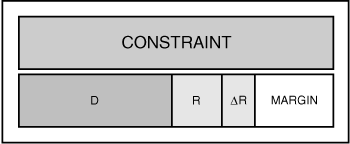
Operating Margin: the difference between a physical constraint and the sum of all parameters and variations in these parameters that could violate the constraint.
Imagine a sixteen-foot semi truck that has to pass under a bridge with a seventeen-foot clearance. The distance, D, between the floor and the ceiling of the trailer is static. The radius, R, of the tires varies around some nominal value depending on load, inflation, and temperature. Figure 1.1 captures the fundamental relationship between constraints and margin.
Since digital signal integrity emerged as a discipline in the 1960s, three main signaling paradigms have evolved: common-clock, source-synchronous, and high-speed serial. It would certainly be difficult to identify a unified set of practices for quantifying operating margins that applies equally well to all three paradigms. Even within one paradigm, different applications require different approaches for assigning a number to each effect that encroaches on the design constraints. Nevertheless, all digital interfaces share a common set of limitations:
- The number of picoseconds in a clock cycle (or unit interval) is finite.
- If the input to the primary flip-flop is not in a stable and correct state when the clock samples it, a bit error will occur.
- Because a receiver is really an amplifier, its output will become highly sensitive to unpredictable noise events if the signal amplitude at its input drops low enough.
- If a noise event at a receiver input is strong enough to cross into the threshold region, the output will switch.
These concepts form the basis for developing a strategy for quantifying the operating margins of any digital interface. The exact form a strategy may take is not as important as the exercise of examining all significant detractors from operating margin and assigning a number to each one. In fact, the form may vary widely from design to design, engineer to engineer, and company to company. If an engineer is fortunate enough to encounter a design that is relatively similar to its predecessor, the strategy may not need to change at all. Colleagues may take issue with the numbers or how to combine them, but that healthy exchange cannot take place unless somebody makes an initial estimate.
Engineers tend to develop their own unique bag of tricks that emerge from the evolutionary process of learning. This book is intended to help fellow signal integrity engineers add to their bag of tricks by challenging them to think deeply about how the fundamental sources of pathological effects in digital interfaces combine to form a fault condition. The maturing discipline of signal integrity demands an increasing level of accuracy and precision from each of us. Although the Holy Grail of failure prediction may never be found, the process of looking for it will produce more reliable digital systems.
A Sadly Familiar Tale
Project Coyote took off like a roadrunner from the very beginning. Conceived in a boardroom behind closed doors at Acme Inc., it was already well-defined before anyone in development engineering heard of it. The senior engineering staff voiced their opinions about the unrealistic schedule, especially during a time when other high-profile projects were consuming most of the company's resources. However, commitments to customers were already made, a marketing plan was in the works, finances were allocated, and the wheels were in motion: the first domino in a sequence of related events.
The second domino was in place before printed circuit (PC) board placement and routing began. The Vice President of Engineering had defined a budget that was consistent with the price point marketing deemed to be competitive, and this budget called for a four-layer PC board: signal-ground-power-signal. Upon seeing the form factor for the first time, the PC board designer expressed concern about routability in certain areas he perceived to be bottlenecks. The signal integrity engineer assigned to this project expressed her concern about high forward crosstalk due to microstrip transmission lines and high edge rates in the PCI Express signals. However, neither she nor the board designer was able to prove that a solution did not exist, so the design progressed as planned.
An exceptionally aggressive schedule became domino number three. In order to meet the schedule, the board design shop had two of their top designers working back-to-back 12-hour shifts for three weeks with one day off on the weekends. While it is true that an auto-router can save many hours of human labor, there is no substitute for an experienced designer when channels are fully allocated. Although the company's design process called for routing constraints to be in place before routing could begin, schedule won the day, and routing began before the signal integrity team was able to assign constraints to the 800 of 1,000 nets on the board that required their attention.
In a remarkable feat of skill and sweat, the design team generated Gerber files on schedule. Much to their credit, they reserved one day for a complete design review with mandatory attendance by everyone on the team. They even invited a few seasoned veterans who had since gone on to jobs in other parts of the company. It was one of these veterans who spotted the problem: a PCI Express differential pair routed next to an Inter-Integrated Circuit (I2C) clock signal. Running at 2.5 Gbps, PCI Express signals swing about 500 mV single-ended in 100 ps for an average edge rate of 3 V/ns 20-80%. He correctly guessed that the edge rate of the I2C clock was lower than this, making it vulnerable to crosstalk from aggressors with higher edge rates, but this information was unavailable on the component datasheet. Anne, the signal integrity engineer assigned to this project, took an action item to acquire IBIS models for the buffer driving the I2C clock, but the vendor required the company to sign a non-disclosure agreement before releasing the IBIS models. The legal process took much longer than the one day allocated for reviewing the design, and the team sent out the Gerber files to the PC board manufacturer. Domino number four.
Power On
The first set of boards came back from assembly and performed admirably on the bench top. The hardware team did their job measuring thermal characteristics, calculating power draw, and capturing bus transaction traces on the logic analyzer. Programmers sifted through register dumps and debugged their code. Knowing there was a possible exposure to crosstalk problems, Anne probed around the board while the other team members were out for a caffeine break. She found low levels of quiet line noise—for example, 200 mV on a 2.5 V signal. No cause for alarm. After two weeks of intense work, the development team declared the board ready for pre-production testing, and everyone left work early to celebrate.
The first sign of trouble arose in the final days of pre-production testing. A set of boards was in the thermal chamber undergoing stress testing at temperature and voltage corners when one of them crashed during a boot cycle, leaving little useful information in the registers. They pulled the board out of the chamber and attempted to repeat the fail on the bench top. No luck. The experienced engineers on the team collectively cringed, remembering painful 14-hour days on another project with a similar irreproducible error. Back to the chamber and still no luck. How worried should they be about this phantom error? It only occurred once while stressing voltage beyond design limits in an attempt to emulate the spectrum of silicon processing variations they expected to see in manufacturing. One could make a strong argument that silicon and voltage stresses produce different failure mechanisms. Are the test results truly representative of actual operating conditions?
Then the phantom reappeared, this time on the bench top while someone happened to be watching the console. The processor had just finished loading boot code and was passing control to the bridge chip to initialize the PCI Express interface. This serial number failed more than once, although not on every boot. The next morning during the daily meeting, the team discussed their options. Hearing the words "PCI Express initialization" reminded Anne of the design review and the I2C clock. She convinced the team to set up two parallel tests probing the I2C clock and its PCI Express neighbor using a glitch detect trigger. They repeatedly booted each board watching for the telltale crosstalk signature.
Their persistence and patience finally paid off when the gremlin surfaced again several days later during the middle of the graveyard shift around 3:00 am. Since I2C and PCI Express are asynchronous to one another, the board only crashed when timing conditions were exactly right for the PCI Express crosstalk to superimpose on the I2C clock while it was passing through the threshold region. The sharp, low-amplitude crosstalk caused a brief slope reversal in the slower I2C clock edge—just enough to clock the input latch twice and upset the state machine.
For a while, the engineers on the development team were elated at having found clear evidence pointing to the origin of the fault. Then reality set in: There was little to be done about it. It is not possible to slow down the edge rate on a PCI Express net. Someone would need to notify management, and that unpleasant job fell to Anne as the signal integrity engineer. They did not receive the news well but were at least decent enough to realize that they had set the stage by proceeding with an extremely aggressive project without gathering input from those responsible for making it happen. Management asked development engineering for a recovery plan.
The following day, the team isolated themselves in a conference room with a white board, pizza, caffeinated beverages, and mandatory cell phone silence. Adding layers to the board and rerouting did not appeal to anyone. Just when they had run out of ideas, Bob the veteran popped his head in the door because word of their dilemma had reached him and he was curious about how things were proceeding. Not very well, they explained, and invited him to listen in for a few minutes. Bob had earned a great deal of respect among his colleagues by observing intently, listening thoughtfully, and not opening his mouth until he had formed a well-founded opinion. When he finally spoke, people's ears perked up.
"What kind of package does your I2C buffer use?"
"TSSOP."
"Good. I was hoping you wouldn't say BGA. Why don't you lift the lead of the clock output pin and insert a snappy little high-bandwidth FET? This will sharpen up the I2C clock so the crosstalk will simply roll off the edge a bit rather than cause a slope reversal."
It may look good on the balance sheet to hand out pink slips to experienced engineers like Bob from time to time, but when they walk out the door, their experience goes with them. After implementing Bob's fix, the gremlin disappeared for good. Project Coyote was out of the ditch—for the time being.
The Long Reach of Legacy Design
Once again things seemed to be proceeding better than any engineer had a right to expect. Pre-production testing completed only a few days behind schedule. The team had closed all outstanding issues that arose during testing. Limited-availability hardware was in the hands of a few beta customers who were running their most strenuous loads. The contract manufacturer had finally optimized the solder profile, and board assemblies were starting to roll off the line with an acceptable defect level.
Unknown to the heroes of our story, another domino was falling at a distant semiconductor manufacturing plant. The board contained a 100 MHz synchronous DRAM interface that was several years old, and this interface used a memory address buffer that had been in production and was nearing end of life. The application required a relatively small amount of memory, and the original designer had opted to implement the interface directly on the board rather than using a DIMM. The current designer simply copied the schematics from a previous project. Nobody got too concerned because the interface had been functioning without trouble for so long. In the rush to market, long-term availability took a back seat.
The output impedance of the address buffer was a critical parameter in the DRAM interface. Each pin of the buffer had to drive four x8 DRAMs to make a 32-bit word—much less challenging than the eighteen loads typically found on an ECC DIMM. The 18-load application called for a low output impedance in the neighborhood of 15 ![]() . The 4-load application needed 40
. The 4-load application needed 40 ![]() . The same vendor had been supplying the contract manufacturer with address buffers for years but had recently fallen out of favor for cost reasons. Unfortunately, the new vendor used the same part number for the low- and high-impedance versions of the chip because none of their customers required them to specify output impedance on their datasheet. Seeing very little demand for the high-impedance buffers, they discontinued production and switched their entire output volume over to the 15
. The same vendor had been supplying the contract manufacturer with address buffers for years but had recently fallen out of favor for cost reasons. Unfortunately, the new vendor used the same part number for the low- and high-impedance versions of the chip because none of their customers required them to specify output impedance on their datasheet. Seeing very little demand for the high-impedance buffers, they discontinued production and switched their entire output volume over to the 15 ![]() buffer. Nobody knew the difference until the 100 MHz SDRAM interface on the Coyote boards started throwing parity errors during beta testing at a customer site. CEOs traded voicemails, and alarms started sounding again at Acme, Inc.
buffer. Nobody knew the difference until the 100 MHz SDRAM interface on the Coyote boards started throwing parity errors during beta testing at a customer site. CEOs traded voicemails, and alarms started sounding again at Acme, Inc.
Anne had worked on a memory interface as a summer intern and was able to proceed through the failure analysis process with calmness and confidence. Her first order of business was to trace the history of the 100 MHz SDRAM interface back to its conception. She spoke with designers from the previous three projects that had used this interface. Each one had simply copied that schematics from their predecessor without performing any timing or signal analysis. At that point, the trail went cold. Nobody knew who the original designer actually was or if that person even was still an Acme employee. Anne decided to do her own timing budget using the datasheets and IBIS models available to her.
She pieced together the clock-to-output time from the buffer chip, the setup and hold times from the DRAM, and the clock chip pin-to-pin skew specification. Using the IBIS models she found on the Internet together with the datasheets, she ran a few quick behavioral simulations to determine how much the actual interconnect delay varied from the standard load listed in the component datasheet and documented her results using a simple spreadsheet timing budget (see Table 1.1). This was where things got interesting.
Table 1.1. 100 MHz SDRAM Address Timing Budget

The new buffer vendor supplied an IBIS model for only the 15 ![]() buffer but did not distinguish between the two parts anywhere in the model. The old vendor supplied IBIS models for both parts, clearly labeling which was which. The IBIS models for the old vendor's parts passed the syntax checker, came with a quality rating, and ran the first time. The IBIS models for the new vendor were full of bugs and would not run. Technical support did not respond to her phone calls or emails, so she did the debugging herself.
buffer but did not distinguish between the two parts anywhere in the model. The old vendor supplied IBIS models for both parts, clearly labeling which was which. The IBIS models for the old vendor's parts passed the syntax checker, came with a quality rating, and ran the first time. The IBIS models for the new vendor were full of bugs and would not run. Technical support did not respond to her phone calls or emails, so she did the debugging herself.
Her simulation analysis of the 40 ![]() buffer showed some gradually undulating reflections superimposed on an RC ramp. The 15
buffer showed some gradually undulating reflections superimposed on an RC ramp. The 15 ![]() buffer overdrove the net severely and caused a strong reflection that rang back into the threshold region of the DRAM receiver while the clock was sampling the address signal. A classic interaction of signal quality and timing: The interface met its timing constraints using the 40
buffer overdrove the net severely and caused a strong reflection that rang back into the threshold region of the DRAM receiver while the clock was sampling the address signal. A classic interaction of signal quality and timing: The interface met its timing constraints using the 40 ![]() buffer but produced a setup time failure with the 15
buffer but produced a setup time failure with the 15 ![]() buffer. The solution to this problem was straightforward: Use the parts from the more reliable vendor and qualify a second vendor.
buffer. The solution to this problem was straightforward: Use the parts from the more reliable vendor and qualify a second vendor.
Reflections on a Near Disaster
The situation could have been much, much worse. Finding two low-level hardware faults so close to production is painful, but it is nothing compared to a line-down crisis. In response to these two close calls, Acme asked Bob to lead an all-day process review; he helped the team retrace the trail that led to the failures:
- The signal integrity team did not have a representative at the table when the architecture was being defined. A cross-disciplinary design team is the cornerstone of a healthy, solid design process.
- There was no cost-performance analysis of the PC board stack-up. This is admittedly one of most difficult things any engineer has to do.
- Schedule should never take precedence over product quality unless the risk of non-functional hardware is deemed acceptable.
- High-quality models are hard to come by, but it is possible to have the models in place when they are needed by planning ahead and involving procurement.
- If a design is sensitive to edge rate and output impedance, then the component datasheet should specify these parameters.
- A signal integrity engineer needs to evaluate every net in a design and make a decision about the appropriate level of analysis required for that net or group of nets. The decisions may range from no analysis at all to a thorough electrical characterization of each component in the net and end-to-end coupled simulation of the IO circuits and everything in between.
During the review, Bob pointed out that both failures were, at their root, timing failures. Crosstalk from the PCI Express net occurred at the same time the I2C clock was switching through its threshold. The reflection on the memory address net occurred at the same time the DRAM was sampling it.
Circumstances do not usually present themselves in such an obvious logical progression as they did in this fictional scenario. It is only careful retrospection that reveals the sequence of events that led to a particular conclusion. To some degree, the job of the engineer is to play the role of the seer, who can predict these circumstances and avoid them without becoming a whiner to whom nobody pays much attention.
It must be tempting for those who are making weighty architectural decisions during the earliest stages of a new product to avoid addressing implementation details. As any experienced engineer will attest, there is usually a price to be paid for defining architecture without input from those whose job it is to implement the architecture. The worst possible scenario is a product that is marginally functional—except the marginal part does not become apparent until production is in full swing. This is even more treacherous than the product that overruns its budget, misses its milestones, and never makes it to market at all. Assembly lines come down. Companies—more than one—lose large quantities of money each day. There may be recalls. There will certainly be redesigns under intense pressure. At the end of the whole experience lies a painful loss of reputation. This is a scenario that no Vice President of Technology or Chief Financial Officer would choose to put in motion if the choice were made clear.
One thing is crystal clear: A company greatly enhances its chance for success by building a cross-disciplinary team in the early architectural phases of the project. In addition to a system architect, a minimum team would include a board layout designer, firmware programmer, and engineers from the following disciplines: logic, software, mechanical, thermal, power, manufacturing, electromagnetic compliance, and signal integrity. A large company may have separate engineers to represent each of these disciplines, while in most other companies, one engineer plays several roles. In any case, it is vital that each discipline have representation at the table and the resources to do their job.
Motivations to Develop a Simulation Strategy
Most signal integrity engineers would agree that the primary motivation for simulating chip-to-chip networks is to maximize the probability that those networks will function flawlessly on first power-up. There is another compelling motivation that is easy to overlook under the intense pressure of time-to-market: understanding operating margins. It is tempting to stitch together IO circuit and interconnect models, run the simulations, check the results, and be done with the exercise. This may prove that the network will function under a given set of conditions, but will the network continue to function reliably over the range of manufacturing and operating conditions it will encounter during the useful life of the product? What are the expected primary failure mechanisms, and how do they interact with one another?
These questions lie at the heart of signal integrity engineering, and it may be possible to answer them given unlimited resources and time. Unfortunately, most signal integrity engineers are operating under somewhat different circumstances. A contemporary PC board design may have thousands of nets that belong to two or three dozen different buses. The power spectrum for these nets will likely have significant content above 5 GHz. Supplying power and cooling to high-performance processors and low-performance chips on 20 different power supply voltages can place challenging constraints on layout and routing.
On top of these technical challenges, the customer may require that the product be ready for manufacturing in a time period that severely stresses the ability of the team to carry out the level of analysis required to ensure reliable operation. This is the irony of the business: The relevant physical effects become ever more difficult and expensive to analyze while the market relentlessly exerts downward pressure on cost and schedule. Two freight trains are running full speed toward each other on the same track.
Given these technical and business challenges, is it still possible to achieve the goal of reliable operation of a system filled with dozens of digital IO buses over the lifetime of the product? At times it may appear that the solution to this difficult problem is the empty set. In the heat of battle, the level of complexity can be so overwhelming that it seems impossible to satisfy all the constraints simultaneously. Nevertheless, it is possible to successfully manage the signal integrity of a complex contemporary design if the team develops a comprehensive simulation and measurement strategy that applies the appropriate level of analysis to each net in the system.
The Boundaries of Simulation Space
Although it is certainly possible to acquire models for a thousand nets and simulate every one of them prior to releasing a design to manufacturing, this approach does not improve corporate profitability. One of the more critical system design exercises is establishing the boundaries of simulation space; that is, what criteria determine whether a net needs to be simulated or whether some other method of analysis is more appropriate. Simulation is expensive and should only be used when there are strong economic and technical motivations for doing so. Once you answer this critical question of whether or not to simulate, then you can get about the tasks of actually running the simulations and interpreting their results.
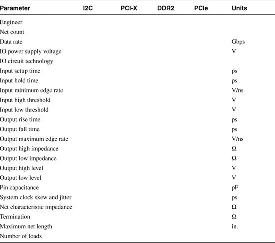
An excellent place to begin the decision-making process is to compile a comprehensive list of all nets in the design and some relevant information associated with each interface or group of nets. The spreadsheet in Table 1.2 forms a skeleton that allows the signal integrity engineer to view the relevant electrical parameters at one glance and make a decision regarding the level of analysis necessary to ensure reliability over the lifetime of the product.
Table 1.2. Analysis Decision Matrix
The simplest case might be an interface that a trusted colleague has analyzed in the past and others have used successfully time and again. In this case, no simulation is required—providing that the combination of the electrical parameters is close enough to the one that was analyzed in the past.
In order of increasing complexity, the next case is the interface for which a design guide or specification exists. If a third party analyzed the interface and published a set of rules that, when followed, will guarantee sufficient operating margins, then simulation is not necessary and the job of the signal engineer defaults to describing design constraints to the CAD system and checking that they are met.
Some interfaces may not require simulation but do require rudimentary hand calculation, such as the value of termination resistors, stub length as a function of rise time, or RC time constant of a heavily loaded reset net. In fact, there is a strong case to be made that every interface deserves a basic set of hand calculations since it is possible to run simulations and still not understand the physics!
Finally, if an interface passes through each of the previous three filters, it is time to assemble the models and fire up the simulator. Not surprisingly, the fastest interfaces require the most accurate models and intense analysis effort. Operating margin estimates are another indicator of effort required; the lower the margins, the more effort. The closer the sorting and analysis process occurs to the beginning of the project, the higher the likelihood of success. If the signal integrity engineer and the person drawing the schematics can agree on a naming convention that involves adding a prefix to the net name of each net in an interface, this will facilitate tracking coverage of all nets in a design.
The goal is to evaluate each net in the system and make a data-driven decision about how best to utilize the skills at your disposal.