
2. Chip-to-Chip Timing
As signal integrity engineers, we need to understand and quantify the dominant failure mechanisms present in each digital interface if we wish to achieve the goal of adequate operating margins across future manufacturing and operating conditions. In an ideal world, we would have time and resources to perform a quantitative analysis of the operating margins for each digital interface in the system, but most engineers do not live in that world. Instead, they must rely on experience and sound judgment for the less-critical interfaces and spend their analysis resources wisely on the interfaces that they know will have narrow operating margins. Regardless of company size or engineering resources available, the goal of any successful signal integrity department is to perform the analysis and testing required to ensure that each interface has enough operating margin to avoid the associated failure mechanisms.
Most signal integrity engineers would agree about the fundamental causes of signaling problems in modern digital interfaces: reflections, crosstalk, attenuation, resonances, and power distribution noise. Although these physical phenomena may be part of a complex and unique failure mechanism process, the end result of each process is the same: a storage element on the receiving chip fails to capture the data bit sent by the transmitting chip. Because on-chip storage elements (flip-flops and registers) are typically beyond the scope of the models used in signal integrity simulations, it is easy to forget that the actual process of failure involves not just voltage waveforms at the input pin of a chip, but a timing relationship between those waveforms and the clock that samples the waveform. In fact, the appearance of the waveform itself may be quite horrible so long as its voltage has the correct value when the clock is sampling it.
Root Cause
A virtual tour of an integrated circuit (IC) chip would uncover one or more flip-flops in close proximity to each signal IO pin. A driver or receiver circuit connects directly to the chip IO pin, and a flip-flop usually resides on the other side of the driver or receiver. The purpose of a digital interface is to transmit a data bit stored on the driving chip and reliably capture that same data bit some time later on the receiving chip. However, there is one caveat to the process: The data signal must be in a stable high or low state at the moment when the flip-flop samples it—that is, when the clock ticks. Because IC chips are subject to variations in manufacturing and operating conditions, the moment of stability translates to a window in time during which the data signal must remain stable. In essence, the job of the signal integrity engineer is to ensure that the data does not switch during this window.
The next few paragraphs offer a functional description of one type of CMOS latch and the associated flip-flop. Not all CMOS flip-flops are identical, but this particular circuit lends itself well to description. It may seem that a discussion of latches and flip-flops is too fundamental to bother with in a text on timing for signal integrity. Careful consideration of these fundamentals, though, lays a foundation for understanding more complicated topics like writing IO timing specifications for an ASIC or measuring bit error rate. If you feel the need for a CMOS refresher, take a brief detour to Appendix A, "A Short CMOS & SPICE Primer."
CMOS Latch
At the heart of a latch lies a pair of pass gates. When the clock is low, the lower pass gate (P1 in Figure 2.1) allows data at the input, D, to flow through the latch to the output Q. When the clock rises to a high state, the lower pass gate closes to block the data from the input, while the upper pass gate (P2 in Figure 2.2) opens to hold the output in the state that it was just before the clock switched low. The mechanism for accomplishing data storage is positive feedback through inverters I4 and I5, which sample the outputs of both the lower and upper pass gates and feed them back to the input of the upper pass gate. When the lower pass gate is no longer open because the clock switched high, the upper pass gate turns on and activates the positive feedback loop. This allows the output of the upper pass gate to reinforce its input and hold the state of the data until the clock switches high again. The inverters I1 and I2 provide differential copies of the clock to the gates of the pass gates, as is necessary for their operation. The inverter I6 ensures that the sensitive internal data node is isolated from the next stage of logic; it also preserves the polarity of the output data, Q, with respect to the input data, D.
Figure 2.1. CMOS latch in open state
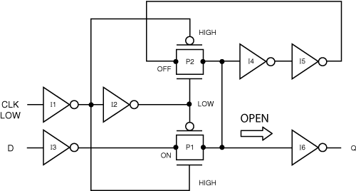
Figure 2.2. CMOS latch in closed state

The problem with a latch is that it only stores data for half the clock cycle, which is not terribly efficient. During the other half, the output simply mimics the input, which is not terribly useful. Figure 2.3 depicts this behavior. If one had a latch that stored data when the clock was high and another kind of latch that stored data when the clock was low, as described in Figure 2.4, this would cover the entire clock cycle. This is precisely what a flip-flop does. It is easy enough to arrive at a circuit that stores data during the high part of the clock cycle by swapping the connections from the clock inverters to the pass gate's inside latch. Connecting these two kinds of latches in series creates a flip-flop. But how does a flip-flop work?
Figure 2.3. CMOS latch timing diagram
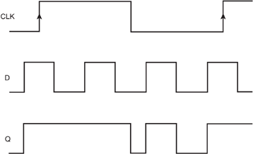
Figure 2.4. CMOS flip-flop timing diagram

When the clock transitions from a low state to a high state, the lower pass gate in the first latch closes off, while the upper pass gate in the first latch opens to "capture" the data that was waiting at the input to the flip-flop when the clock switched high. During the time before the clock switched high, the data at the input of the flip-flop also showed up at the input of the second latch but did not make it any further because the second latch was in its closed state at the time. Now that the clock is high, any change in data at the input of the flip-flop goes no further than the first inverter. The flip-flop is essentially regulating the activity of all circuits that precede it.
Because the pass gates in the second latch have inverted copies of the clock, the second latch goes into its open state at the same time the first latch goes into its closed state. This means that the data stored by the first latch immediately passes through the second latch and shows up at the output of the flip-flop—after some brief propagation delay. When the clock switches high, it also "launches" the data that was present at the input of the flip-flop on to whatever circuitry is connected to the output of the flip-flop.
The first latch holds the data that was present at its input when the clock switched high for the remainder of the clock cycle. When the clock falls low, the second latch transitions back into its closed state, blocking the data path again and storing the data that the first latch was holding for it. Now the first latch goes back into its open state and allows the new data to enter it, ready to be latched again the next time the clock rises.
Timing Failures
The previous discussion assumed that the data at the input of the flip-flop was in a stable state when the clock switched high. What would happen if the data and the clock were to switch at the same instant in time? CMOS logic is made from charge-coupled circuits. In order to change the state of the feedback pass gate in a flip-flop, it is necessary to move charge from one intrinsic capacitor to another. Some of this capacitance is a part of the transistor itself; a gate insulator sandwiched between a conductor and a semiconductor forms a capacitor. Some of the capacitance is associated with the metal that wires transistors together. It takes work to move electrons, and the alternating clock signals on either side of the feedback pass gate provide the energy to do the work.
If the data happens to change at the same time as the clock is doing its work, it robs the circuit of the energy that it was using to change the state of the latch. Not good. The result is metastability, an indeterminate state that is neither high nor low. This state may persist for several clock cycles, and it throws a wrench into the otherwise orderly digital state machine. Chip designers strive to avoid this troublesome situation by running timing analyzer programs during the process of placing and routing circuits. Signal integrity engineers strive to avoid the same situation, although their tools differ. Many of us are used to running voltage-time simulators, but few of us use timing analyzers.
The dual potential well diagram in Figure 2.5 is a useful analogy for visualizing the physics of metastability. Imagine a ball sitting at the bottom of a curved trough that is separated from an identical trough by a little hill. The first trough represents a latch that is in a zero state, and the second trough represents the same latch in a one state. Moving the ball from the first trough to the second requires the addition of some kinetic energy to get over the hump between the troughs. If the kinetic energy is just shy of the minimum threshold required, the ball may find itself "hung up" momentarily on the hill between the two troughs in a state of unstable equilibrium. A little bit of energy in the form of noise will push the ball into either of the two troughs.
Figure 2.5. Dual potential well model for CMOS latch

Setup and Hold Constraints
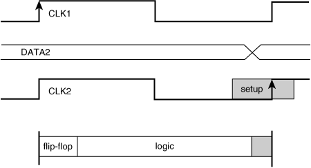
In order to prevent the condition of metastability from occurring in a flip-flop, the circuit designers run a series of simulations at various silicon manufacturing, temperature, and voltage conditions. They carefully watch the race between the data and clock signals on their way from their respective inputs to the four pass gates inside the flip-flop, as well as the time it takes for the upper pass gates to change state. Based on the sensitivity of these timing parameters to manufacturing and operating conditions, they establish a "safety zone" in time around the rising edge of the clock during which the data must not switch if the flip-flop is to settle in a predictable state when the clock is done switching. The beginning of this safety zone is called the setup time of the flip-flop, and the end is called the hold time (see Figure 2.6). These two fundamental circuit timing parameters form the foundation for the performance limitations of a digital interface.
Figure 2.6. CMOS flip-flop setup and hold times

The modern CMOS chip is a gigantic digital "state machine" that is governed by flip-flops, each of which gets its clock from a common source through a distribution network. In between the flip-flops lie various CMOS logic circuits that perform functions such as adding two binary numbers or selecting which of two data streams to pass along to the next stage of logic. Naturally, data do not pass through these logic circuits instantaneously. A circuit's characteristic propagation delay varies with the number and size of transistors and the metal connecting the transistors together.
Consider this simplest of state machines in Figure 2.7. When the left flip-flop launches a data bit into the first inverter in the chain at the tick of the clock, the data must arrive at the input of the right flip-flop before the tick of the next clock—less the setup time. If the data arrives after the setup time, the right flip-flop may go metastable or the data may actually be captured in the following clock cycle. In either case, the timing error destroys the fragile synchronization of the state machine, and the whole system comes to a grinding halt. This failure mechanism is called a setup time failure, and Figure 2.8 illustrates the timing relationship between data and clock. Depending on where you work, it may also be called a late-mode failure or max-path failure.
Figure 2.7. On-chip timing path

Figure 2.8. Setup time failure
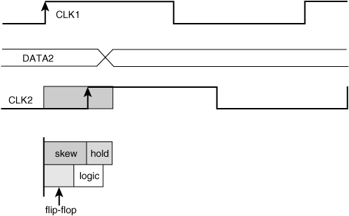
Now imagine that the clock signal does not arrive at both flip-flops at the same time. This is not an uncommon problem as there are so many flip-flops that all get their clocks from the same source. Just like everything else in the world, it is impossible to design a perfectly symmetrical clock distribution scheme that delivers a clock to each flip-flop in a chip at the same time. The difference in arrival times of two copies of the same clock at two different flip-flops is called clock skew.
Imagine that clock arrives at the capturing flip-flop later than the launching flip-flop. Now imagine that the propagation delay of the logic circuits, including the launching flip-flop, is smaller than the clock skew. In this case, the second flip-flop will capture the data during the same cycle it was launched—that is, one cycle early. Figure 2.9 depicts this condition. This failure mechanism is called a hold time, early-mode, or min-path failure, and it is the more insidious of the two failures because the only way to fix it is to improve the clock skew or add more logic circuit delay, both of which require a chip design turn. The setup time failure can be alleviated by slowing the clock. In order to prevent a hold time failure from occurring, it is necessary to ensure that the the sum of flip-flop and logic propagation delay is longer than the sum of the clock skew and the flip-flop hold time.
It took a few iterations for me to absorb the concept of hold time failure. To aid my understanding, somebody gave me an illustration early in my career that I will pass along to you. Imagine a long hallway of doors spaced at regular intervals. The doors all open at the same instant and remain open for a fixed period of time. A man named Sven is allowed to run through exactly one door at a time, after which all doors slam shut again at the same instant and remain closed before opening again and sending Sven on his merry way. Consider four cases, as follows:
- If Sven is in good physical shape and times his steps, this process can continue indefinitely.
- If Sven needs a membership at the health club, he may find himself in between the same two doors for two slams—or longer.
- If Sven happens to be an overachiever, he may make it through two doors before hearing the last one slam behind him.
- Sven runs into the door just as it is slamming in his face.
These four cases correspond, respectively, to reliable data exchange, setup time failure, hold time failure, and metastability.
Common-Clock On-Chip Timing
The name common clock describes an architecture in which all storage elements derive their clocks from a single source. In a common-clock state machine, clock enters the chip at a single point, and a clock tree re-powers the signal to drive all the flip-flops in the state machine. The clock originates at an oscillator, and a fan-out chip distributes multiple copies of that clock to each chip in the system. The problem with the common-clock architecture is that copies of the clock do not arrive at their destination flip-flops at exactly the same instant. When clock skew began consuming more than 20 or 30 percent of the timing budget, people started looking for other ways to pass data between chips.
The SPICE simulation entitled "On-Chip Common-Clock Timing" illustrates setup and hold failures. This simple network comprises two flip-flops separated by a non-inverting buffer whose delay the user may alter by selectively commenting out two of the three instances of subcircuit x2. Clock sources vclk1 and vclk2 also need adjustment. Clock vclk1 (node 31) launches data from flip-flop x1, and clock vclk2 (node 32) samples data at flip-flop x3. In the default configuration of this deck, whose waveforms are shown in Figure 2.10, vclk1 launches data on the first clock cycle, vclk2 captures that data on the second clock cycle 5 ns later, and all is well. See Appendix A for a discussion of SPICE simulation basics.
Figure 2.10. Nominal on-chip timing
On-Chip Common-Clock Timing
*----------------------------------------------------------------------
* circuit and transistor models
*----------------------------------------------------------------------
.include ../models/circuit.inc
.include ../models/envt_nom.inc
*----------------------------------------------------------------------
* main circuit
*----------------------------------------------------------------------
vdat 10 0 pulse (0 3.3V 1.0ns 0.1ns 0.1ns 6.0ns 100ns)
* nominal clocks
vclk1 31 0 pulse (0 3.3V 2.0ns 0.1ns 0.1ns 2.4ns 5ns)
vclk2 32 0 pulse (0 3.3V 2.0ns 0.1ns 0.1ns 2.4ns 5ns)
* hold time clocks
*vclk1 31 0 pulse (0 3.3V 2.0ns 0.1ns 0.1ns 2.4ns 5ns)
*vclk2 32 0 pulse (0 3.3V 2.5ns 0.1ns 0.1ns 2.4ns 5ns)
* setup time clocks
*vclk1 31 0 pulse (0 3.3V 2.0ns 0.1ns 0.1ns 2.4ns 5ns)
*vclk2 32 0 pulse (0 3.3V 1.5ns 0.1ns 0.1ns 2.4ns 5ns)
* d q clk vss vdd
x1 10 20 31 100 200 flipflop
* nominal delay buffer
* a z vss vdd
x2 20 21 100 200 buf1ns
* hold time delay buffer
* a z vss vdd
*x2 20 21 100 200 buf0ns
*setup time delay buffer
* a z vss vdd
*x2 20 21 100 200 buf5ns
* d q clk vss vdd
x3 21 22 32 100 200 flipflop
*----------------------------------------------------------------------
* run controls
*----------------------------------------------------------------------
.tran 0.05ns 20ns
.print tran v(31) v(32) v(21) v(22)
.option ingold=2 numdgt=4 post csdf
.nodeset v(x1.60)=3.3 v(x1.70)=0.0
.nodeset v(x3.60)=3.3 v(x3.70)=0.0
.end
Setup and Hold SPICE Simulations
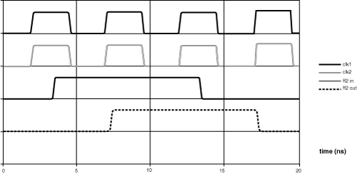
In the setup time failure depicted in Figure 2.11, the first flip-flop launches its data during the first clock cycle, but the data does not arrive at the second flip-flop until after the second clock cycle, which means the second flip-flop does not capture the data until the third clock cycle. Clock skew exacerbates the problem by advancing the position of the second clock with respect to the first (clock skew = 2.0 ns – 1.5 ns = 0.5 ns). The sum of the flip-flop delay, non-inverting buffer delay, and setup time is greater than the clock period, and a setup time failure occurs.
Figure 2.11. On-chip setup time failure

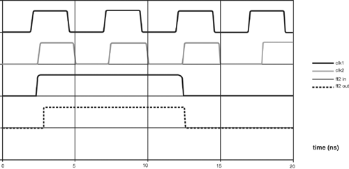
Figure 2.12 demonstrates the other extreme: the hold time failure. The combined delay of the first flip-flop and the non-inverting buffer is less than the sum of the hold time of the second flip-flop and the clock skew (clock skew = 2.0 ns - 2.5 ns = -0.5 ns). The second flip-flop captures the data during the same clock cycle in which the first flip-flop launched the data, and a hold time failure occurs.
Figure 2.12. On-chip hold time failure
Timing Budget
The simple spreadsheet timing budget in Table 2.1 expresses the relationship between each of these delay elements and the corresponding timing constraints: one column for setup time and one column for hold time. Notice that the setup column contains an entry for the clock period while the hold column does not. That is because a hold time failure occurs between two rising clock edges separated by skew in the same clock cycle; it is entirely independent of clock period, which is why you cannot fix this devastating problem by simply lengthening the clock cycle. (Take it from one who knows: Devastating is no exaggeration.) The setup time failure, on the other hand, occurs when the sum of all timing parameters is longer than the clock period.
Table 2.1. On-Chip Timing Budget
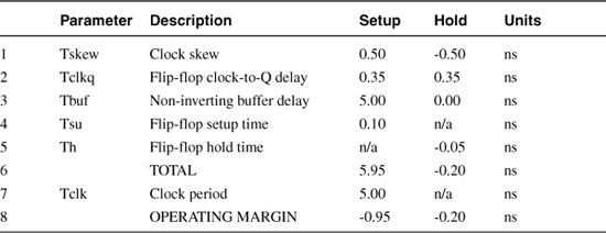
The second thing to notice is that flip-flop hold time only appears in the hold column, while flip-flop setup time only appears in the setup column. These two numbers represent the boundaries of the metastability window. The setup column numerically describes the physical constraint that data needs to switch to the left of the metastability window as marked by the setup time at the next clock cycle. The hold column conveys a very different idea: Data cannot switch during the same clock cycle it was launched before the metastability window, as marked by the hold time.
Finally, the reason the hold column contains negative numbers is because the hold time failure is a race between delay elements (protagonists) on one side and the sum of clock skew and hold time (antagonists) on the other side. Therefore, the delay elements are positive, while the clock skew and hold time are negative. Summing all hold timing parameters in rows 1 through 5 results in a positive operating margin when the hold constraints are met and a negative margin when they are not. The numbers in rows 1 through 5 of the setup column are all positive, and setup operating margin is the difference between the clock period and the sum at row 6. Clock skew always detracts from operating margin.
This somewhat artificial example swaps three different delay buffers into the x2 subcircuit under nominal conditions that, of course, would never happen in a real chip. Setup and hold timing analysis on an actual design proceeds by subjecting the logic circuits between two flip-flops to the full range of process, temperature, and voltage variations. To accomplish this in SPICE, the example decks in this chapter call an include file, which in turn calls one of three transistor model parameter files for fast, slow, and nominal silicon. It also sets the junction temperature and power supplies.
*----------------------------------------------------------------------
* transistor model parameters
*----------------------------------------------------------------------
.include proc_nom.inc
*----------------------------------------------------------------------
* junction temperature (C)
*----------------------------------------------------------------------
.temp 55
*----------------------------------------------------------------------
* power supplies
*----------------------------------------------------------------------
vss 100 0 0.0
vdd 200 0 3.3
vssio 1000 0 0.0
vddio 2000 0 3.3
rss 100 0 1meg
rdd 200 0 1meg
rssio 1000 0 1meg
rddio 2000 0 1meg
The fast and slow transistor model parameter files call the same set of parameters as the nominal file but pass different values representing the predicted extreme manufacturing conditions over the lifetime of the semiconductor process. A typical range of junction temperatures for commercial chips might be 25–85 C. Processor chips often run hotter. Chip designers commonly use +/- 10% for power supply voltage variation, but a well-designed power distribution network seldom sees more than +/- 5% from dc to 100 MHz. Transient IO voltages may droop more than 5% when many drivers switch at the same time, but that is the topic of another book.
Common-Clock IO Timing
Several factors make timing a common-clock digital interface more complicated than timing an on-chip path:
- Delay from the chip clock input pin to the flip-flop (clock insertion delay)
- Skew between clock input pins on the driving and receiving chips
- Combination of driver and interconnect delay
- Receiver delay
A good part of this additional complexity is hidden beneath chip timing specifications. However, it is important to understand these underlying complexities, especially when writing timing specifications for a new ASIC.
* a oe pad vss vdd vssio vddio
x2 20 200 21 100 200 100 200 drv
t1 21 0 22 0 td=1ns z0=50
* a z vss vdd
x3 22 23 100 200 rcv
The differences between the on-chip and IO SPICE decks are not many. A driver, transmission line, and receiver replace the string of inverters. In addition to data input and output pins, the driver also has an output enable input pin (oe) that, when high, takes the driver out of its high-impedance state and allows the output transistors to drive the transmission line. An extra set of power supply rails (vssio and vddio) isolates the final stage of the driver from the core power and ground busses; the transient currents moving through the final stage are so large that the voltage noise they generate is best kept away from the core circuitry of the chip. Chapter 3, "Inside IO Circuits," discusses electrical characteristics and modeling of a few simple IO circuits.
The ideal transmission line models a point-to-point connection between two chips on a printed circuit board. Typical common-clock interconnect simulations involve a multi-drop net topology, lossy transmission lines, chip packages, and maybe a connector or two. The clock trees in Figure 2.13 appear in the timing budget but not in the simulation; they are simply too large to include in signal integrity simulations. The clock distribution chip does not appear in this simulation, either, although it is important to simulate these nets separately, as clocks are some of the most critical nets in any system.
Figure 2.13. Common-clock interface

When the input to the clock distribution chip switches, a clock signal travels down the wire from the output of the clock chip to the clock input of Chip 1, where the clock tree distributes it to every flip-flop on the chip. When the flip-flop in front of the driver sees the rising edge of the clock, it grabs the data at its input and launches it out toward the driver, which re-powers the data and sends it off the chip and down the interconnect—a 1 ns 50 ![]() transmission line, in this case. After a delay of 1 ns, the data signal shows up at the input of the receiver.
transmission line, in this case. After a delay of 1 ns, the data signal shows up at the input of the receiver.
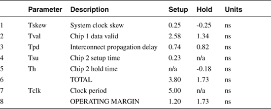
Meanwhile, a clock signal from the second tick of the clock travels from the clock chip to Chip 2, through its clock tree, and arrives at the clock input of the flip-flop on the other side of the receiver. If all goes well, the data signal will arrive at the data input of the flip-flop on Chip 2 slightly before the clock signal does—with a difference of at least the setup time. To ensure that this is always the case, you must construct a timing budget similar to Table 2.1 but with extra terms to account for the additional complexity. Table 2.2 adds three new lines.

As was the case of the on-chip timing budget, clock skew comes right off the top and counts against margin. The IO budget must account for system clock skew in addition to variation in two on-chip clock trees (rows 2 and 5 in Table 2.2). System clock skew has at least three possible origins. The output pins on the clock distribution chip never switch at exactly the same instant in time, and there is a specification in the chip datasheet for this. There are also differences in propagation delay down the segments L1 and L2. Even though these may be in the same printed circuit board, there will be layer-to-layer variation in dielectric material and trace geometry. Finally, the two chips will not have identical loading.
The timing budget in Table 2.1 assumed both flip-flops were on the same chip and neglected the clock insertion delay, defined as the difference in time between the switching of the chip's clock input and the arrival of that clock at the flip-flop. (This definition of clock insertion delay encompasses on-chip clock skew.) If clock insertion delay were identical for both chips, it would add to Chip 1 delay and subtract the same number from Chip 2 delay. However, silicon processing and operating conditions introduce variations that complicate things.
Assume the two chips depicted in Figure 2.13 are identical, and their nominal clock insertion delay is 0.3 ns. This delay is probably realistic for a 0.5 μm CMOS technology, which was state-of-the-art at the same time as 200 MHz common-clock systems. Also assume that the clock tree has a process-temperature-Voltage tolerance of 50%—a little worse than the transistor models predict for this imaginary CMOS process.
In the hold timing budget, worst-case timing occurs when the data path looking back from the capturing flip-flop is fast and the clock path looking back from the capturing flip-flop is slow. Tracing from the flip-flop data input on Chip 2 all the way to the source of the clock, which is the clock distribution chip, the clock tree on Chip 1 is actually in the data path. This implies that the clock insertion delay number in row 2 of the timing budget needs to be at its smallest possible value to generate worst-case hold conditions. Worst-case conditions for a setup time failure are the converse of those for a hold time failure. A large clock insertion delay on Chip 1 implies that the data arrives at the target flip-flop on Chip 2 later in time; this condition aggravates setup margin.
The flip-flop delay, setup, and hold times are present as they were in the on-chip budget. New to the budget is the combined delay of the driver and transmission line, considered here as one unit because the delay through the driver is very much a function of its loading. This delay is defined as the difference between the time when the driver input crosses its threshold, usually VDD/2, and the time when the receiver input exits its threshold window, usually some small tolerance around VDD/2 for a simple CMOS receiver. Note that the percent tolerance of this delay is less than it is for circuits on silicon because the transmission line delay is a large portion of the total delay, and its tolerance is zero for the purposes of this analysis.
Things get a little tricky on rows 5 and 6 because there is a race condition between the clock path and the data path on Chip 2. Using worst-case numbers for both these delays would result in an excessively conservative budget because process-temperature-Voltage variations are much less when clock and data circuits reside on the same chip. A crude assumption would be to simply take the difference between the nominal clock insertion delay of 0.3 ns and the nominal receiver delay of 0.17 ns. The clock would arrive at the flip-flop 0.13 ns later than the data if they both arrived at the pins of Chip 2 simultaneously. Clock insertion delay at Chip 2 is favorable for setup timing but detrimental for hold timing. To obtain a more accurate number, consult a friendly ASIC designer and ask for a static timing analysis run.
As in the on-chip budget, the hold timing margin is simply the sum of rows 1 through 8. Clock period does not come into play in a hold budget because all the action happens between two rising edges of the same clock cycle that are skewed in time. Setup timing margin is the clock period, 5 ns, less the sum of rows 1 through 8.
Early CMOS system architects realized that clock insertion delay was a pinch-point for CMOS interfaces, so they began using phase-locked loop circuits (PLLs) to "zero out" clock insertion delay at the expense of jitter and phase error. Contemporary digital interfaces rely heavily on PLLs, and signal integrity engineers need to pay close attention to PLL analog supplies to keep jitter in check.
Common-Clock IO Timing Using a Standard Load
Unless they are directly involved in designing a new ASIC, signal integrity engineers do not typically have access to on-chip nodes in their simulations. If they succeed in convincing a chip manufacturer to part with transistor-level driver and receiver models, they can connect a voltage source to the input of a driver and monitor the output of a receiver. But that is where it ends. IBIS models are the standard for interfaces running slower than 1 Gbps (they are capable of running faster), and IBIS only facilitates modeling that part of the IO circuit connected directly to the chip IO pad. This situation is not entirely unfavorable since chip vendors are forced to write their specifications to the package pin, a point accessible to both manufacturing final test and the customer. Having access to only the driver output and receiver input simplifies the chip-to-chip timing problem considerably—assuming the chip vendor did a thorough job writing the chip timing specifications.
How does a chip designer arrive at IO timing specifications that are valid at the package pins rather than the flip-flop? For input setup and hold specifications, they begin with the flip-flop setup and hold specifications and take into consideration the difference between the receiver delay and the clock insertion delay, including both the logic gate delays and the effects of wiring. Looking back from the flip-flop on the receive chip, the receiver circuit is in the data path and the clock tree is in the clock path.
Therefore, to specify a setup time requirement at the package pins, they consider the longest receiver delay and the shortest clock insertion delay. Conversely, the hold time specification involves the shortest receiver delay and the longest clock insertion delay. Because both the receiver and the clock tree are on the same chip, their delays will track each other and never see the full chip-to-chip process variation. In addition to the on-chip delays, the setup and hold time specifications must also account for variations in package delay.
Chip output timing specifications are also relative to the package pins. The output data valid delay for a chip, sometimes called clock-to-output delay, is a combination of clock insertion delay, flip-flop clock-to-Q delay, and driver output delay with one caveat: The delay of the driver is a function of its load, and the driver may see a wide variety of loading conditions that are unknown to the chip designer.
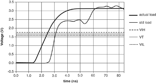
The standard load or timing load resolves this ambiguity. The standard load usually comprises some combination of transmission line, capacitor, and termination resistor(s) intended to match a typical load as the chip designer perceives it. Along with the standard load, the vendor also specifies a threshold voltage that defines the crossing points for both the clock input and the data output waveforms. The output data valid specification quantifies the delay between the clock input switching and the data output switching, each through their corresponding thresholds, with the standard load connected to the package output pin. As a signal integrity engineer, your job is to understand and quantify the difference between the standard load and your actual load.
Extracting timing numbers from simulation using a standard load is straightforward. Simulate the driver with its standard load alongside the driver, interconnect, and receiver in the same input deck, as shown in Figure 2.14, using the same driver input signal for both copies of the driver. The interconnect delay timing interval begins when the output of the standard load driver crosses the threshold, VT, specified in the chip datasheet and ends when the input of the receiver crosses one of the two threshold values, VIH and VIL, that define its switching window.
Figure 2.14. Actual load and standard load

The fast interconnect timing interval in Figure 2.15 begins when the standard load crosses VT and ends when the actual load crosses VIL for the first time. Because the fast case corresponds to a hold time analysis, we use the earliest possible time the receiver could switch. In Figure 2.16, the slow interconnect timing interval begins when the standard load crosses VT and ends when the actual load crosses VIH for the last time. The longest possible interconnect delay is consistent with a setup time analysis. Of course, some pathological combination of reflections could always result in the fast case producing the worst-case setup delay, so it pays to consider the possibilities.
Figure 2.15. Fast interconnect delay with standard load

Figure 2.16. Slow interconnect delay with standard load
This analysis assumes no crosstalk-induced delay. Further discussion on the relationship between crosstalk and timing will follow in Chapters 6, "DDR2 Case Study," and 7, "PCI Express Case Study."
*----------------------------------------------------------------------
* circuit and transistor models
*----------------------------------------------------------------------
.include ../models/circuit.inc
.include ../models/intercon.inc
.include ../models/envt_fast.inc
*.include ../models/envt_nom.inc
*.include ../models/envt_slow.inc
*----------------------------------------------------------------------
* main circuit
*----------------------------------------------------------------------
vdat 10 0 pulse (0 3.3V 1.0ns 0.1ns 0.1ns 6.0ns 100ns)
* actual load
* a oe pad vss vdd vssio vddio
x1 10 200 20 100 200 100 200 drv50
x2 20 21 0 bga_rlc
t1 21 0 22 0 td=1ns z0=50
x3 22 23 0 bga_rlc
* a z vss vdd
x4 23 24 100 200 rcv
* standard load
* a oe pad vss vdd vssio vddio
x5 10 200 40 100 200 100 200 drv50
x6 40 41 0 bga_rlc
c1 41 0 10pF
Note that it is possible to have a negative interconnect delay if the actual loading conditions are lighter than the standard load. This does not mean the signal is traveling faster than the speed of light! Rather, it is simply an artifact of the vendor's choice for standard load and the signal integrity engineer's choice of net topology. If the vendor chose a 50 pF standard load and you are timing a T net topology with two 5 pF loads at the end of a 4 in. transmission line, the actual load will switch before the standard load. In fact, the choice of standard load is not terribly significant so long as the simulations use the same load specified in the component datasheet.
It is also possible for the fast interconnect delay to be larger than the slow interconnect delay, as is the case for this configuration of driver and net. This looks strange in the budget, but rest assured that the sum of the fast driver and interconnect delays is actually smaller than the same sum in the slow case, as Table 2.3 proves. This is just another artifact of the choice of standard load.
Table 2.3. Driver and Interconnect Delay

The IO timing budget in Table 2.4 closely resembles the on-chip timing budget in Table 2.1 with Chip 1 taking the role of the first flip-flop, Chip 2 taking the role of the second flip-flop, and interconnect delay replacing the non-inverting buffer delay. It is somewhat unusual to see a 0.41 ns setup and hold window in a datasheet for a chip running at 200 MHz. Although this is not difficult to achieve in silicon with a 0.5 μm CMOS process, chip vendors prosper when specifications are conservative and final test yields are high.
Table 2.4. IO Timing Budget Using Standard Load
Signal integrity engineers prosper when they successfully design and implement reliable digital interfaces. This fundamental conflict of interests often makes it difficult for signal integrity engineers to close timing budgets on paper. Fortunately, contemporary industry standard specifications that evolved with input from the user community have more realistic timing numbers.
Receiver thresholds are another area of creeping conservatism. Chapter 3 will demonstrate that the actual receiver input window within which a receiver's output will transition from low to high is very narrow—on the order of 10 mV. Yet a typical VIH/VIL range for 3.3 V CMOS logic is 1.4 V, which is an artifact of transistor-transistor logic (TTL) legacy.
The two dashed lines in Figures 2.15 and 2.16 represent VIH and VIL at fast and slow process-temperature-Voltage corners. At least two philosophies exist for defining interconnect timing. In the first philosophy, setup timing uses the longest interconnect interval defined by the latest receiver threshold crossing; that is, VIH for the rising edge and VIL for the falling edge. Hold time timing uses the first VIL crossing for the rising edge and the first VIH crossing for the falling edge.
The second camp maintains the position that thresholds track with VDD by a factor of 50% for a typical CMOS receiver. Why time the receiver to fast thresholds when the driver is at low VDD? The two will never be off by more than 1% or 2% for a well-designed power delivery system. Personally, I favor the second philosophy because so many engineers contribute conservatism to the chip-to-chip timing budget. I don't like to hold performance hostage to anxiety. In this example, I used this second approach, but there was not much difference between the two because the receiver thresholds came from simulations of the receiver. When receiver thresholds come from a conservative component specification, the difference can be substantial.
Limits of the Common-Clock Architecture
The common-clock IO timing budget demonstrates how large-scale distribution of a low-skew clock caps system performance somewhere between 200 and 300 MHz. Supercomputer makers were able to push this to 400 MHz, but not without a huge investment in custom technology. Multi-drop net topologies impose their own set of limitations. In the past decade, point-to-point source synchronous and high-speed serial interfaces became the bridges that enabled the next level of system performance.
Chapters 6 and 7 are case studies in two industry standard interfaces, DDR2 (source synchronous) and PCI Express (high-speed serial). Getting these interfaces to run reliably requires both an understanding of the timing constraints and a set of models whose accuracy is consistent with the task at hand. Toward that end, Chapters 3 through 5 take a close look at modeling the IO circuits and interconnect components found between the flip-flops. Even though you may not be in the business of developing these models yourself, a thorough understanding of them is a prerequisite for accurate timing and signal analysis.
The common-clock architecture is still alive and well in digital systems everywhere. Although it may not be exciting to work on these nets, ignoring them is sure to bring more trouble than any signal integrity engineer would care to deal with. Any time the input to a flip-flop violates the setup and hold window, a timing failure will occur, whether the data is switching once every 10 ns or once every 200 ps.