
4. Modeling 3D Discontinuities
Integrated circuits generate electromagnetic waves, but it is the stuff that lies between the chip IO pads that corrupts these waves and erodes operating margins. I use the term "interconnect" to refer to chip packaging, multi-chip modules, sockets, printed circuit boards, connectors, cables, flexible circuits, terminators, filters, passive discrete components—anything that serves as the conduit for a digital signal. These interconnect components are responsible for many of the pathological behaviors that signal integrity engineers have come to know and love so well for the income they bring us: reflections, crosstalk, attenuation, and resonances.
Chapter 3, "Inside IO Circuits," made the argument that understanding IO circuit behavior is essential to preventing failures in digital interfaces. A similar argument applies to interconnect components. More often than not, a signal integrity engineer obtains a model for a connector or a chip package from the component vendor. In some cases, an ambitious person may undertake the time-consuming but rewarding task of developing one of these models from scratch. In either case, designing a reliable digital interface requires a deep understanding of interconnect electrical characteristics, which include propagation delay, impedance profile, crosstalk, and frequency-dependent loss.
This chapter introduces a process for modeling 3D discontinuities using a time-domain electromagnetic field solver. Chapter 5, "Practical 3D Examples," discusses two practical interconnect component examples. Even if you are one of those people who has no intention of ever running a 3D field solver, I encourage you to read through Chapters 4 and 5 because their insight into interconnect models will help you in acquiring and using these models. In the years ahead, the most successful signal integrity engineers will be those who are able to expand their vision beyond voltages and currents and into the realm of electromagnetic fields.
Beyond Transmission Lines
Most electrical engineers who graduated from college between 1960 and 1980 are comfortable with the idea that cables and copper traces in a printed circuit board can behave like transmission lines. When these engineers were kids, they rummaged through junk piles looking for parts to build their own amateur radio set. Early in life, they encountered transmission lines in the form of coaxial cables.
The PC revolution and ensuing explosion of the global electronics industry dramatically altered the economic landscape, as well as the after-school hobbies of an entire generation of future engineers. Kids who grew up in the 1980s and 1990s were more likely to take an interest in computer programming and the Internet than amateur radio. Despite the dramatic differences between these two generations of engineers, there is one thing they have in common: the required electromagnetic fields class. This class was a polarizing experience. Students either loved it or hated it.
Regardless of which category you fall into, the relentless march of technology is pressing us to stretch the boundaries of our minds beyond the comfortable concepts of impedance, propagation delay, capacitance, and inductance (well, maybe inductance was not so comfortable) and into the sometimes-distressing realm of invisible three-dimensional vector fields.
There is no doubt that this is a difficult subject. The math associated with electromagnetics is intense: divergence, gradient, curl, and partial differential equations. It is a sad fact that only the simplest electromagnetic field problems can be solved analytically, and the solutions to these "simple" problems are often aggravatingly complicated. To top it off, many of the quantities involved are ones for which measurement instruments do not exist. For most people, it takes a lot of meditation before the basic concepts of electromagnetic field theory begin to sink in—some would even say a lifetime of meditation.
If you are in need of a brief and, I hope, readable refresher on electromagnetic fields, you may wish to spend half an hour reading through Appendix B, "A Stroll Through 3D Fields."
Finite Difference Time Domain Method
Thankfully, computer algorithms and their underlying hardware platforms have evolved to the point where they are able to give the determined user a beautiful graphical rendering of an electromagnetic wave flowing through an arbitrary configuration of conductors and dielectric material. Algorithms like the Finite Difference Time Domain (FDTD) method[10] have presented us with a singular opportunity that would have awed physicists of the 1800s: the ability to describe a general electromagnetic field problem to a computer and have it return a timely and economical solution that offers valuable insight into the physical system. As with anything else in nature, this opportunity does not come for free. The user must acquire enough understanding about what the field solver is doing to allow him or her to guide the software to a meaningful—and correct—solution.
The FDTD method is simple enough that it is possible to solve a one-dimensional problem using a spreadsheet, and that is exactly what Drs. Ward and Nelson of the Massachusetts Institute of Technology did.[11], [12] Their paper is a short, readable, and excellent introduction to the topic of 3D numerical electromagnetic field analysis. The method begins with the discretization of space and time. All numerical methods involve approximations to the analytical equations derived from first principles, and a good code will strike a balance between error and run time while minimizing instability, the numerical condition that causes a program to throw up its hands and say, "I quit."
Time stepping is a concept familiar to users of SPICE or any other time-domain circuit solver. Buried somewhere inside the computer code for one of these solvers lies a statement that looks like this:
t = 0;
for (n = 0; n <= nmax; ++n)
{
t = t + dt;
}
In plain English, the code instructs the computer to start at time zero, let n be the counter of time steps, and let its value vary between zero and some maximum integer, nmax, that determines the end of the simulation. Then increment this counter (++n) each time through the loop, and use it to calculate the new value of time (t) from the previous value of time and the time step (dt). In SPICE, the natural time constants of the circuits determine the largest allowable time step required for accurate results. In FDTD, the size of the spatial mesh cell and the speed of light determine the upper limit of the time step.
Making the time step too large will result in the solver "stepping over" interesting variations in the fields and returning misleading results. The algorithm may even become unstable, and the field quantities may blow up. Making the time step too small will result in excessive run time and unnecessary consumption of computer resources. Fortunately for the user, both SPICE and 3D time-domain field solvers handle the time step size internally.
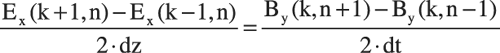
Spatial discretization is not so familiar to SPICE users; circuit models assume that all elements reside at the same location in space (with the exception of transmission lines). To get a clear picture of how spatial discretization works in the FDTD method, it is helpful to consider the simple one-dimensional problem of propagation through a vacuum with no charge present as Ward and Nelson did in their spreadsheet example. In this case, Maxwell's third and fourth equations reduce to simple partial derivatives in space and time. If the wave propagates along the z-axis, the electric field has only an x-component and the magnetic field has only a y-component. According to Maxwell, the spatial derivative of the electric field (Ex) is proportional to the time derivative of the magnetic field (By) and vice versa.

![]()
These equations apply to a continuous distribution of space and time—not much good to a computer. In order to solve them, the program needs to divide space into discrete cells and then calculate one value for the electric field and one value for the magnetic field at each cell. Let zmin and zmax represent the boundaries of the spatial variable, and let the index k keep track of the spatial location of each discrete cell along the z-axis. The variable dz stores the size of the cell, which is a function of the minimum wavelength.
dz = (zmax - zmin) / kmax;
The centered difference approximation to the derivative samples the function on either side of the point of tangency. Using this approximation, the left-hand term of Maxwell's third equation reads:
![]()
Of course, each electric and magnetic field component is a function of both time (n) and space (k). We can rewrite Maxwell's third and fourth equations using this notation and the central difference approximation. The time index remains fixed in the expression for the space derivatives, and the space index remains fixed in the expression for the time derivatives.

The FDTD method employs a slightly different set of calculations. By mixing up the indices in a clever trick called interleaving, FDTD accounts for the conditions imposed by Maxwell's first two equations, which have not come into play until this point.
Figure 4.1 depicts three cells in one-dimensional space at two points in time. The spatial variable (k) increases from left to right, and time (n) increases from top to bottom. The bold rectangle indicates the active cell (k,n) whose values of Ex and By the program is currently calculating. The active electric field variable Ex takes its value from the previous value of Ex at the same location and the difference between the two previous values of the magnetic field variable By at the same location and the left neighbor cell. In Figure 4.2, the active magnetic field variable By takes its value fro the previous value of By at the same location and the difference between the active values of Ex a the same location and the right neighbor cell.
Figure 4.1. FDTD Ex calculation

Figure 4.2. FDTD By calculation

The machinery is now in place for computing the propagation of an electromagnetic disturbance through this imaginary one-dimensional medium. The program calculates Ex and By for all points in space at the same time, which comprises one complete time cycle in the algorithm. Then the program increments the time index and repeats the whole procedure again and again until the simulation reaches its conclusion. As in all differential equation problems, it is necessary to define the initial conditions (the stimulus function) at the location where the energy enters the problem and the boundary conditions (the electric and magnetic fields at zmin and zmax).
The wonder of this technique is that it reduces a complicated set of vector equations to a few numerical derivatives, a form that has been familiar to engineers since the early days of freshman calculus. The calculations mimic as closely as numerically possible the actual physical system: a packet of electromagnetic energy enters the problem at one of the boundaries, propagates through the volume, scatters off any discontinuities it encounters, and eventually exits the volume. The field solver systematically calculates the values of the electric and magnetic fields at each mesh cell in the volume and each point in time. As it does this, the stimulus eventually finds its way to every cell in the volume since the derivatives are a function of the most immediate neighbor cells.
Although signal integrity engineers certainly do not need enough knowledge to write their own 3D field solver, the ability to visualize what is going on when a field solver runs will help them with tasks such as choosing boundary conditions or evaluating mesh density. A 3D field solver is an invaluable vehicle for exploring the behavior of electric and magnetic fields in the time domain. This knowledge, when applied to practical interconnect structures, will go a long way toward the design of robust digital interfaces.
If this all seems baffling, come back another day and read it again. I certainly did not get it the first time through, and I fall into the category of people who loved field theory.
Solo Flight in a 3D Field Solver
It may be possible to jump into the left seat of an automobile without any instruction and get from point A to point B alive. It may also be possible to jump into the left seat of an airplane cockpit without any instruction and leave the ground, but holding the aircraft just above stall speed until the wheels touch the ground is an entirely different trick than parking a car. Nevertheless, just about anyone can learn to do it with a good flight instructor in the right seat.
Like an aircraft, the 3D field solver gives its pilot the chance to see the world from a different perspective. It allows the determined signal integrity engineer to break free from the one-dimensional bonds of current and voltage and begin to see the signal path the way the signal sees it: as a conduit for transferring electromagnetic energy from point A to point B. There are obstacles along the path, places where energy may become trapped or redirected. There are places where multiple paths converge and exchange energy. Other simulators will never illuminate these obstacles and help the signal integrity engineer understand them the same way a 3D time-domain field solver does.
Some have described SPICE as a virtual oscilloscope that allows the user to probe the function of a circuit without having to actually build it. In a similar way, a 3D time-domain field solver allows the user to probe into the physics beneath the interconnect and see things that cannot be seen any other way. It is an indispensable tool, and it is possible to solo one in a relatively short time—although mastering it takes considerably longer!
The process of 3D electromagnetic modeling follows a basic flow:
- Pre-modeling—that is, defining the problem to yourself and gathering information.
- Describing the problem to the field solver (hopefully the same problem).
a. geometry
b. materials
c. ports
d. boundary conditions
- Configuring the run controls.
- Evaluating the mesh.
- Turning the solution engine loose.
- Checking and interpreting the results.
- Extracting a network model; for example, distributed RLC, equivalent circuit, s-parameters.
- Verifying the model.
Coaxial Transmission Line
When embarking on a journey into a new body of knowledge, a familiar milestone is always a good place to begin. This allows the traveler to turn around, take a benchmark from the previous milestone, and know the current position. The coaxial transmission line is one of those problems with an "aggravatingly simple" solution. Because of its simple geometrical structure, it has an analytical solution that doesn't involve complex numerical approximations.

![]()
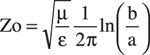
In these equations, derived from applying the laws of Ampere and Gauss, the variable a is the radius of the center conductor and b is the radius of the shield. The two constants ε and μ are the electric permittivity and magnetic permeability, respectively, of the dielectric material between the center conductor and the shield. In anticipation of solving printed circuit board vias, the slice of coaxial transmission line in this first 3D model has the following parameters:
a = 10 mils
b = 53 mils
ε = 4.0 x εo = 4 x 8.85e-12 C2/Nm2
μ = μo = 1.26e-06 N/A2
Using Equations 4.4–4.6, you should verify that this is indeed a 50 ![]() coax. Conveniently, the choice of 4.0 for the dielectric constant implies that electromagnetic radiation will travel at half the speed of light down this transmission line.
coax. Conveniently, the choice of 4.0 for the dielectric constant implies that electromagnetic radiation will travel at half the speed of light down this transmission line.
CST Microwave Studio (CST MWS), by Computer Simulation Technology of Darmstadt, Germany, will serve as the reference solution engine for the 3D electromagnetic field problems in this chapter. Although CST MWS employs the Finite Integration Technique (FIT), which casts Maxwell's equations in integral form rather than differential form, the preceding discussion on the FDTD method is still relevant. The math involved in FIT is more complicated and also more general than FDTD, but FIT still divides the volume into an orthogonal mesh and calculates the values of the electric and magnetic fields at each cell in the mesh as the wave propagates through the volume.
Defining the coaxial transmission line model to the field solver begins with units and coordinate system. Units may seem like a trivial detail, but be sure to set them before drawing any shapes. Although the choice of units for frequency, time, and distance is not critical, they must be consistent with other parameters in the model—for example, the time axis of a user-defined stimulus waveform or a solid imported from a mechanical CAD tool. The coordinate system in CST MWS is always a three-dimensional Cartesian space, and the user must choose how to align the structure with the coordinate system. A judicious choice can simplify the drawing of three-dimensional shapes, improve efficiency, and lower the chances of making mistakes.
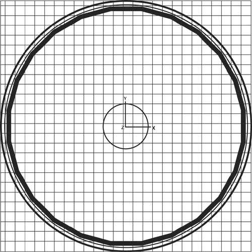
The geometry of this model corresponds to a 10 mil plated through hole with a 53 mil antipad. Actual vias pass through a stack of planes rather than a solid shield, so their impedance can still be close to 50 ![]() even though their antipad diameters are smaller. For this problem, the units are mils, GHz, and ns. The z-axis is common with the axes of the center conductor and shield. This simplifies port definition and field visualization.
even though their antipad diameters are smaller. For this problem, the units are mils, GHz, and ns. The z-axis is common with the axes of the center conductor and shield. This simplifies port definition and field visualization.
Boundary Conditions
Once you have drawn the two concentric cylinders made from perfect electrical conductor (PEC), the next step is to define the conditions at the outer faces of the bounding box that encloses everything in the 3D problem. The outside dimensions of the structure define the actual size of the bounding box. Normally this is one of the more critical steps in defining the problem, but the coaxial transmission line contains all the energy within the outer shield so the boundary conditions in Figure 4.3 are irrelevant.
Figure 4.3. Boundary conditions

There are two general kinds of boundaries available to the user: absorbing and reflecting. The open boundary absorbs all energy incident upon it. The electric reflecting boundary forces the tangential component of the electric field to zero. Similarly, the magnetic reflecting boundary forces the tangential component of the magnetic field to zero. If you know ahead of time that there will be a reflecting condition at the boundary or that the conditions at the boundary do not matter, a reflecting boundary will save calculations. However, defining a reflecting boundary may create a resonant cavity that can introduce artificial behavior not present in the physical system. Choose boundary conditions wisely.
Waveguide Ports
CST MWS offers two means for injecting a signal into the problem: a point source or a waveguide port. The point source has its uses, but the models in this book employ waveguide ports because they provide a precise mechanism for delivering energy to the discontinuity that is consistent with the structures found in printed circuit boards and IC packages. A waveguide port carries a transverse electromagnetic (TEM) wave within close proximity of the discontinuity so the field solver can calculate how the TEM mode breaks up and then forms again on the other side of the discontinuity, just as it does in an actual physical system—such as a backplane connector between two striplines. As such, waveguide ports should mimic real-life transmission line structures, like coaxial cables or striplines, which typically have an impedance of 50 ![]() single-ended or 100
single-ended or 100 ![]() differential.
differential.
In CST MWS, waveguide ports are coplanar with the faces of the bounding box. The center of the port should touch the face of the signal conductor, and the edges should touch the return conductors. The stimulus energy emanates from within the two-dimensional area of the waveguide port; at time zero, there is no energy anywhere else within the boundaries. As a matter of habit, I make the distance between the port and the discontinuity long enough that trailing edge of the Gaussian pulse at the port dies out before the energy from the leading edge reflects back to the port. This way, the non-TEM modes around the discontinuity do not interfere with the TEM modes the field solver enforces at port. This principle does not apply to the coax model because there are no discontinuities.
In Figure 4.4, the bold black rectangle is the first waveguide port. The second port is parallel to the first and resides on the opposite side of the coax. The small arrow in the lower-left corner of the rectangle indicates the direction of energy flow; it must point into the problem space.
Figure 4.4. Coaxial waveguide port

Stimulus Function
The next step involves configuring the stimulus function. In CST MWS, the default stimulus function is a Gaussian pulse whose width is tied to the maximum frequency run control: the higher the maximum frequency, the shorter the pulse width. A TDR step function is also available, or the user may import a custom waveform. The Gaussian pulse offers computational advantages when CST MWS transforms the time-domain results into the frequency domain. If s-parameters are the desired output, use the default Gaussian stimulus.
Because wavelength determines mesh density, the maximum frequency strongly influences the physical correctness of the field solution. Setting the maximum frequency too low will cause important field gradients to fall between the corners of mesh cells. The field solver will faithfully execute the algorithm and propagate a wave through the structure, but it will skip over important features whose granularity falls below the size of a mesh cell. The resulting solution may be unstable or just plain wrong. On the other hand, setting the maximum frequency too high will cause the solver to generate an excessive number of mesh cells. Simulations will run much longer than necessary and consume more memory.
Signal integrity engineers are familiar with the equation that describes the bandwidth requirements for a digital interface that must propagate a given rise time to the receiver:
Will Equation 4.9 correctly predict the maximum frequency requirement for a general 3D field simulation? The coaxial transmission line in this model is 68 ps long (2 x 85 ps/in x 0.4 in), so it is reasonable that a waveform whose rise time is 32 ps will allow an accurate representation of the propagation delay extracted at the 50% points. If the rise time is longer than the electrical length of the coax, the edge will not fit in the coax at one time! According to Equation 4.9, 32 ps corresponds to a frequency of 16 GHz.

In this model, 16 GHz is high enough to produce physically correct results for wave propagation through a simple coaxial structure that is 400 mils long. However, models extracted from 3D field simulations must also faithfully reproduce the sharp waveform features associated with noise pulses and the corners of fast edges. For this reason, Equation 4.9 is not generally sufficient for all electromagnetic models. Common rules of thumb range from two to five times the normal bandwidth predicted by Equation 4.9. Be aware that pushing the frequency too high may excite resonances beyond the band of interest. The best advice is to explore the sensitivity of the simulation results to maximum frequency. An occasional model-to-hardware correlation exercise, while expensive, will keep your evolving electromagnetic solution recipe on track.
Mesh Density
With a maximum frequency of 16 GHz and the default mesh parameter settings, the field solver generates a mesh that is 27 nodes in the x direction, 27 nodes in the y direction, and 46 nodes in the z direction, for a total of 30,420 nodes. The node count is the number of mesh cell vertices that lie within the bounding box: 30,420 = 26 x 26 x 45. Inspecting the mesh visually is a critical step toward ensuring the quality of the results since the mesh cells must be small enough to provide a reasonable approximation to the finest structures of interest in the problem. Be sure to examine the finest features in the structure for sufficient mesh coverage. Figure 4.5 shows that only 16 cells cover the circular center conductor, yet the solver still produces physically correct results. The example of differential vias in Chapter 5 discusses mesh density in further detail.
Running the Solver
It is finally time to advance the throttle, pull back on the stick, and get the field solver airborne. After you press the "start" button, CST MWS progresses through several steps, including calculating modes, processing excitation, and transient field analysis—that is, calculating E and B as a function of x, y, z, and time. The entire process took only 51 seconds on a 1.5 GHz processor with 8 GB of main memory and actually used less than 1 GB. Naturally, a more realistic problem will consume far more run time and require a good deal more attention to the mesh. It is not unusual for a complex multi-port problem to keep a large machine busy for several days and take several iterations to optimize the mesh. This emphasizes the need to develop disciplined practices that are founded in a sound understanding of the fundamental concepts of 3D field analysis. Unfortunately, these things do not appear to most people in their dreams. The sensible way to advance your level of expertise is to start with simple problems and bridge to more complex ones—stopping along the way to verify some of them in the laboratory.
When the transient solver finishes running, you need to check several indicators of the solution quality:
- Solver log file
- Port signals
- S-parameters
- Energy
The solver echoes to a log file some of the more important settings, such as units, mesh size, boundary conditions, and frequency settings. The user should double-check these against a spreadsheet that stores the "recipe" for running the simulation. This may sound like nit picking, but running a 3D field solver is picky work. First-time users will probably be tempted to skip parts of the process that seems tedious but will inevitably learn to take certain precautions when the results of some long, important, and time-critical simulation turn out to be useless because one of the nits was in the wrong place! Most people would never set foot aboard a jet airliner if they knew the pilot thought checklists were a nuisance and never bothered to look at one.
The amplitudes of the reflected and transmitted waves depend strongly on the impedance of the transmission medium that delivers energy to the discontinuity, and this impedance should be continuous between the port and the discontinuity. S-parameters depend on the impedance of the transmission medium, too. Touchstone files contain an impedance parameter. Check the port impedances reported in the log file and make sure that they are within a few percent of the impedances expected in the actual system interconnect environment. The port impedances for this model are 50 ![]() ±1
±1 ![]() .
.
Port Signals
The port signals folder in CST MWS contains three port waveforms: the Gaussian input pulse from port one, the output at port two from the port one stimulus, and the reflected signal at port one from the port one stimulus. The field solver detected symmetry about the x-y plane, so it never bothered to stimulate port two, which would have yielded identical results. The output at port two from port one (labeled o2,1 in Figure 4.6) is simply the input phase shifted by 68 ps. The simulated delay is accurate within ±1 ps when compared to the delay calculated from the velocity of light and the distance.
Figure 4.6. Input and output waveforms

The reflected signal at port one is nearly zero, as it should be with no dielectric losses, no conductor losses, and no discontinuities. The port signals pass the sanity check—that is, they compare well to expected results. Before pressing the "start" button on any simulator, develop some idea of the expected answer because simulators and models are known to produce non-physical results. Investigating significant discrepancies between results and expectations, while tedious, usually produces a favorable return on invested effort—through filtering bad models, learning, or both.
S-Parameters
CST MWS performs a Fourier transform on the time-domain data to produce s-parameters. Therefore, s-parameters introduce no new information that was not already present in the time-domain port signal waveforms. They simply afford the user a different view of the information that may yield insight into the behavior of the physical system represented by the model. Keep in mind that a great deal of simplification already occurred in reducing 30,420 electric and magnetic field vectors into a time-domain port waveform! Any model derived from the s-parameters will carry along with it the same simplification.
At first glance, s-parameters can seem intimidating to signal integrity engineers, who are usually more comfortable in the time domain. In essence, s-parameters are little more than the Bode plot most electrical engineers saw in freshman circuit analysis. To generate a Bode plot for a network, we simply apply a small-amplitude sine wave to one of its ports and observe the amplitude and phase response at every other port in the network. This is exactly what a vector network analyzer (VNA) does.
The s21 parameter captures the transmitted amplitude and phase response at port 2 when port 1 is stimulated. The s11 parameter captures the reflected amplitude and phase at port 1 when the same port is stimulated, which is a departure from the basic Bode plot. In an ideal interconnect component, s21 will remain flat and close to one over the entire band of interest (low loss), and s11 will be a large negative number (low reflection). Figure 4.7 exhibits these uninteresting characteristics, although no real component will ever look this good. Note that s-parameters display power information, while the Bode plot familiar to electrical engineers typically displays voltage information. The Touchstone file format for s-parameters therefore includes an impedance normalization parameter that allows any software using the s-parameters to transform from the power domain to the voltage domain.

Energy
The energy plot found under the 1D Results folder displays a volume integral of the energy stored in the electric and magnetic fields as a function of time. The units are dB compared against the peak energy. In a typical simulation, the shape of this curve will be that of an upside-down letter U similar to Figure 4.8. The initial energy will be zero before the wave enters through the port at the face of the bounding box. It should peak roughly in the middle of the simulation and then decay back to zero as the wave exits the bounding box.
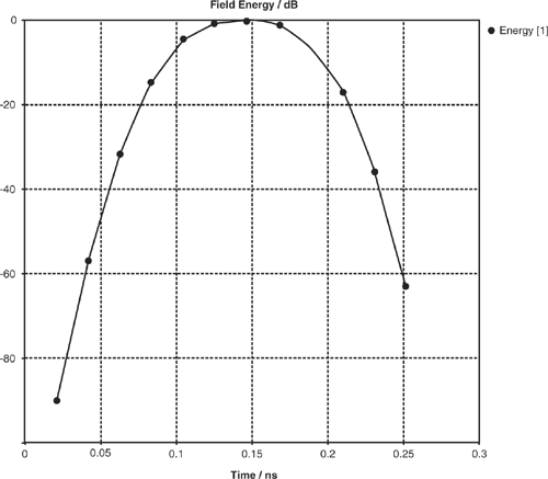
If the structure resonates near the frequencies present in the stimulus waveform, it will trap energy, and the slope on the right-hand side of the U will be less than the slope on the left-hand side. This tail indicates that energy is still present in the structure and is taking a longer time to decay than it would in a non-resonant structure.
CST MWS uses energy as its criterion to determine when a simulation is done. When the energy falls below the accuracy floor defined in the Transient Solver menu, the solver will terminate the simulation. The user must trade off accuracy and run time. Raising the accuracy floor will result in shorter run times, but it will also result in higher residual energy that may become the source of model accuracy problems. For example, the accuracy of the low-frequency points in a set of s-parameters depends on the steady-state solution of Maxwell's equations. If you bump the accuracy limit higher to improve run times, you may also be compromising the integrity of the low-frequency s-parameter information.
Field Visualization
The coaxial transmission line is an excellent example of field visualization since the results are already well known. CST MWS can generate movies of the electromagnetic wave as it passes through the structure. Because the electric and magnetic field vectors are confined to a plane that is perpendicular to the direction of propagation in a TEM wave, we will choose the x-y plane (z=0) as the location at which to visualize these vectors. An actual time-lapse sequence would show the electric and magnetic field vectors grow from zero and swell to their maximum value as the peak of the Gaussian wave passes the x-y plane midway through the simulation. Then they would taper off again to zero as the wave exits the second port. The following two plots depict the electric and magnetic fields frozen at the time when the wave crest passes z=0.
The plots are consistent with electrostatics. Electric field vectors in Figure 4.9 point radially away from the center conductor toward the shield, and they are strongest near the center conductor. Magnetic field vectors in Figure 4.10 swirl around the center conductor in agreement with the right-hand rule and also die out toward the shield. All vectors that lie on the same circle share the same magnitude.
Figure 4.9. E-field at x-y plane

Figure 4.10. B-field at x-y plane

In addition to the electric and magnetic fields, power flow is particularly useful to signal integrity engineers. Engine designers must ensure that the fuel system efficiently directs fuel from the tank, through a fuel injector, into the cylinder, and then out the exhaust system. Signal integrity engineers are engaged in a similar vector flow problem: They design a transit system of silicon and interconnect that directs energy from a transmitter circuit to a receiver circuit without excessive losses along the way. Because system reliability depends directly on the efficient transfer of this energy, it makes sense to pay attention to the vector cross product of the electric and magnetic fields, which measures power flux through a surface.
![]()
The cross product in Equation 4.10 defines a new vector field, called the Poynting vector, which is perpendicular to the electric and magnetic vectors at each point in space. This vector points in the direction that energy is flowing. Because the electric and magnetic field vectors in the coaxial transmission line lie parallel to the x-y plane, the power vector points along the z-axis. The wave enters the volume of the coax as a small clump of vectors clustered around the center conductor. As time progresses, the cluster grows in size and begins traveling along the center conductor toward the second port on the far end. When the wave passes the half-way point, it resembles a shower of arrows from a medieval action film racing toward their targets.
Figure 4.11 demonstrates the power of visualizing electromagnetic vector fields in three-dimensional space and time. Most readers could probably have verbally described how the fields in a coaxial cable behave before reading this chapter, but few electrical engineers have had the opportunity to observe the simulated propagation of an electromagnetic wave using a 3D field solver. It is probably the closest anyone will ever get to seeing Maxwell's Equations in action.
Figure 4.11. Power flux vector field

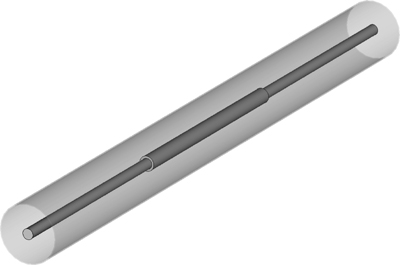
Coaxial Discontinuity
The goal of this chapter is to develop some level of comfort with this powerful tool that is able to produce three-dimensional pictures showing how electromagnetic energy flows through an arbitrary configuration of conductors. On the way to modeling serious interconnect structures, let's take a close look at one of the simplest discontinuities imaginable. The model in Figure 4.12 is a 40 ![]() coaxial segment situated between two 50
coaxial segment situated between two 50 ![]() segments of the same dimensions from the previous problem.
segments of the same dimensions from the previous problem.
Figure 4.12. 50 ![]() coax with 40
coax with 40 ![]() discontinuity
discontinuity
What are the expected results of this simulation? Will they obey the well-known equation for the reflection coefficient at the junction of two ideal transmission lines?

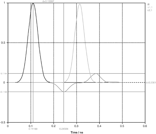
To calculate the fields up to 16 GHz, CST MWS generates a Gaussian pulse whose width is 50 ps at half the maximum value. Because it takes 68 ps for the wave to cross 400 mils at half the speed of light, most of the pulse will fit in each of the three segments—that is, 68 ps in the 50 ![]() segment, 68 ps in the 40
segment, 68 ps in the 40 ![]() segment, and 68 ps in the 50
segment, and 68 ps in the 50 ![]() segment. With the same parameter settings as the first coax problem, the field solver generates a mesh with 93,964 cells (26 x 26 x 139)—almost exactly three times larger than the first coax problem. The run time is three times longer as well. The Finite Integration Technique calculates each electric and magnetic field component using only the field components at the adjacent cells, so run time scales linearly with the number of elements in the mesh.
segment. With the same parameter settings as the first coax problem, the field solver generates a mesh with 93,964 cells (26 x 26 x 139)—almost exactly three times larger than the first coax problem. The run time is three times longer as well. The Finite Integration Technique calculates each electric and magnetic field component using only the field components at the adjacent cells, so run time scales linearly with the number of elements in the mesh.
The time-domain waveforms in Figure 4.13 confirm that the structure does indeed behave like three cascaded ideal transmission lines. The magnitude of the reflected wave matches the traditional equation for the reflection coefficient, ρ, derived from transmission line theory, within two significant digits. The sign of the reflection from the first boundary is negative, and the sign of the reflection from the second boundary is positive—both as predicted. The amplitude of the transmitted wave at the second port is only slightly less than the original incident amplitude at the first port because the transition to the higher impedance region produced a positive reflection, which, when added to the incident wave, bumped it slightly higher. This is consistent with conservation of energy: Because there are no losses and no open boundaries, energy that enters the problem volume must also exit.
Figure 4.13. Input, output, and reflected waveforms
Formation of Reflection
Looking at the power flow vectors, things really get interesting at the first boundary between the 50 ![]() region and the 40
region and the 40 ![]() region. Between port 1 and this boundary, the power wave proceeds along the center conductor, as Figure 4.14 illustrates, with only a z-component, exactly as it did in the first coax problem. Figure 4.15 shows how the vector intensity grows on the left side of the discontinuity as the reflected wave begins to form. At the edge of the junction, some vectors take on a slight x-y component as the wave parts to flow around the larger diameter conductor. Once the wave passes into the 40
region. Between port 1 and this boundary, the power wave proceeds along the center conductor, as Figure 4.14 illustrates, with only a z-component, exactly as it did in the first coax problem. Figure 4.15 shows how the vector intensity grows on the left side of the discontinuity as the reflected wave begins to form. At the edge of the junction, some vectors take on a slight x-y component as the wave parts to flow around the larger diameter conductor. Once the wave passes into the 40 ![]() region, the normal TEM pattern reforms on the other side of the discontinuity with a strength slightly less than that of the first incident wave and no x-y component. A similar phenomenon occurs at the second discontinuity from 40
region, the normal TEM pattern reforms on the other side of the discontinuity with a strength slightly less than that of the first incident wave and no x-y component. A similar phenomenon occurs at the second discontinuity from 40 ![]() back to 50
back to 50 ![]() : The power vector magnitudes peak briefly as the reflection is forming, and then the TEM wave resumes on the opposite side of the discontinuity.
: The power vector magnitudes peak briefly as the reflection is forming, and then the TEM wave resumes on the opposite side of the discontinuity.
Figure 4.14. Power flux vectors just before encountering discontinuity

Figure 4.15. Formation of reflection

The time-domain waveforms from conventional transmission line theory pale in comparison to the three-dimensional sculpture of this complex physical phenomenon that most have only seen on the flat canvas of current and voltage. Unfortunately, books are unable to reproduce a time-lapse sequence.
S-Parameters and Their Explanation
The s-parameters from the simple coax model were simply dull. How do the s-parameters for this model compare to the time-domain and power flow views of this problem? If the reflection coefficient is -0.11, Equation 4.12 might lead us to believe the s11 parameter should equal -19 dB.
![]()
The s-parameters from Figure 4.16 tell a different story. Instead of a flat line at -19 dB, s21 varies between -13 dB and some rather large negative values.

What is the explanation for the shape of these s-parameters? Consider the frequency at which a full sine wave fits into the middle section of the coax:
![]()
At 7.35 GHz, half a sine wave fits exactly into the middle section. When the packet of energy at location B in Figure 4.17 (amplitude +0.89) encounters the second discontinuity, it sends a positive reflection (amplitude +0.098) in the leftward direction. By the time this reflection reaches the first discontinuity, the primary sine wave has traveled half a cycle to the right—just the right distance for the reflection to add to the part of the sine wave, point A, exactly 360 degrees out of phase from the region that generated the reflection. Constructive interference occurs as indicated by a null in the s11 parameter (reflection) and a peak in the s21 parameter (transmission). This problem is just a twist on the classical standing wave—the difference being soft boundaries that pass most of the energy in the wave rather than high impedance boundaries like the ends of a guitar string.
Figure 4.17. Constructive interference at 7.35 GHz

At 3.68 GHz, a quarter wavelength fits into the middle section, and this is a recipe for destructive interference. When point D on the waveform passes the first boundary, 89% of the energy continues in the direction of propagation. The second boundary reflects 11% of that 89% back toward port 1. Because the reflection coefficient at the second boundary is positive and the amplitude at point D is negative, the reflection from the second boundary is also negative. This reflection reaches the first boundary at the same time point C does. The reflection from point C combined with the transmitted reflection from point D gives rise to a peak in s11 at 3.68 GHz.
Figure 4.18. Destructive interference at 3.68 GHz

Ironically, when simulating voltage waveforms and eye diagrams, three ideal transmission lines represent this structure much more efficiently than a set of s-parameters! This reinforces the need to understand the physics, have a general idea of how the simulation results should look, and extract a model that is consistent with the physics.
In complex interconnect problems that defy our sense of intuition gained from experience, a 3D field solver is a powerful tool for deepening our physical knowledge. In the years ahead, the most successful signal integrity engineers will be those who are able to expand their vision beyond voltages and currents and into the realm of electromagnetic fields.