
3. Inside IO Circuits
At first glance, it may seem that signal integrity engineering has more to do with packaging and interconnect technology than it has to do with silicon. After all, signal integrity engineers worry about things like skin effect, dielectric losses, and coupling in three-dimensional structures; transporting electromagnetic energy from point A to point B is the primary goal. However, the output driver circuit is the source of the electromagnetic disturbances, and the receiver circuit must convert the electromagnetic energy incident on its input transistors into digital information. An elementary understanding of IO circuits helps us make decisions about what simulations are necessary to ensure the reliability of a digital interface.
For example, skin effect is a frequency-dependent phenomenon. The frequency content of a driver's output waveform determines whether a lossy transmission line model is required or whether an ideal transmission line is sufficient. Knowledge of a driver's rise time is necessary to make this decision. Unfortunately, the electrical characteristics of an IO circuit are often hard to come by since many chip datasheets still contain only the most rudimentary dc specifications.
An IO Buffer Information Specification (IBIS) model can fill in the gaps, but effective usage of any component model implies a basic knowledge of the assumptions beneath the model. Some circuits make the transition between transistor-level modeling and behavioral modeling naturally, while others get trapped in between because the fundamental set of behavioral modeling assumptions is not consistent with the circuit function. This chapter provides an overview of the "workhorse" CMOS IO circuits and a platform from which to reach the more esoteric circuits.
CMOS Receiver
Although they often go overlooked, receiver thresholds are critical parameters for any digital IO interface. Perhaps the reason they go overlooked is that reliable and useful numbers remain so elusive. They don't need to be, though. Characterizing the input thresholds of a receiver is not difficult.
A receiver circuit interprets the signal on the net and translates it into a language the chip can understand—ones and zeros. The simple CMOS receiver in Figure 3.1 is a pair of inverters. If the n-channel and p-channel transistors have the right dimensions (that is, resistance), the inverter will change states when the input crosses VDD/2 and all four transistors are biased on. At this point, both the n- and p-channels have equal resistance, and the entire circuit functions as a pair of voltage dividers. The output will also be VDD/2.

The dc transfer characteristic in Figure 3.2 plots receiver output voltage against the input voltage, and a close look shows that the receiver does not switch exactly at VDD/2 in a vertical line; there is some region of uncertainty called the threshold window. Traditional circuit analysis defines the boundaries of the threshold window using the unity gain points.
Figure 3.2. Receiver dc transfer characteristic

Consider the receiver circuit as an amplifier. If biased near the threshold, the receiver will amplify a small signal superimposed on the dc bias level. By moving the dc bias level around, you will find two values at which the gain of the amplifier is equal to one—that is, output amplitude equals input amplitude. These are the unity gain points, and the receiver amplifies all signals that are biased between these points. An easier way to find these points is to plot a line whose slope is one on the dc transfer characteristic and find where this line is tangent to the curve. The input voltages that correspond to these two points of tangency are the unity gain points.
The distance in mV between unity gain points for the CMOS receiver in this fictional 0.5 μm circuit library is on the order of 10 mV—next to nothing. Variations in process and temperature affect the size of the threshold window very little, but the receiver threshold for this circuit does track differences between VDD and VSS by a factor of one half. This makes the thresholds sensitive to dc variation in supply voltage, as well as high-frequency ac noise from within the chip and mid- to low-frequency ac noise from without.
Chip designers must either account for high-frequency on-chip ac noise in the timing specifications or in the receiver thresholds. If they choose timing specifications, then typical receiver thresholds for a 0.5 μm CMOS process might vary ±165 mV around 1.67 V—that is, tracking a ±10% tolerance at the VDD pins by one half. If they choose to account for high-frequency on-chip ac noise in the dc input characteristics, the threshold window will probably be slightly larger. They had better not choose both ways!
In either case, the actual receiver threshold window is much narrower than the ancient 0.8 V and 2.0 V TTL specifications commonly seen in 3.3 V parts. If you use TTL specifications to define the right-hand side of an interconnect delay interval, as in Figures 2.15 and 2.16, this extra conservatism translates directly into lower system performance. We might expect IBIS models to contain more accurate threshold voltage numbers since the standard was intended to meet the needs of the signal integrity community, but that is not necessarily the case. It would appear that the authors of many IBIS models simply copy the receiver thresholds directly from the component datasheet rather than extracting them from simulations.
CMOS Differential Receiver
As data rates climbed and supply voltages dropped, low-swing differential signaling technologies became attractive. The CMOS differential receiver resembles the emitter-coupled logic NOR gate (also known as the bipolar differential amplifier) found in Motorola's "MECL System Design Handbook."[1] It is a current-mode circuit in which the two input transistors, M1 and M2, in Figure 3.3 are alternately biased into conduction. Beneath them sits a current source. The two resistors hanging from the VDD rail are really transistors biased into conduction and sized to give the desired resistance.
Figure 3.3. CMOS differential receiver
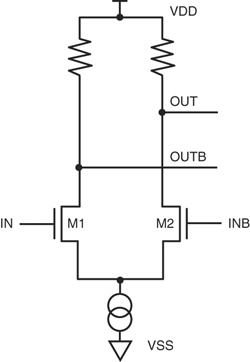
When M1 and M2 are driven differentially, the current from the source sloshes back and forth between the two parallel branches of the circuit, generating a voltage drop across whichever resistor happens to be carrying the current. An alternate implementation biases M2 with a dc reference voltage (Vref) and drives M1 with a single-ended signal.
The differential configuration has the advantage of an effective input edge rate that is twice as high as the single-ended configuration, making the circuit less sensitive to delay modulation induced by crosstalk or reflections. The single-ended implementation uses half as many package pins but requires distribution of a high-quality reference voltage, which is sensitive to noise and requires close attention to layout.
Pin Capacitance
Pin capacitance is yet another source of conservatism. A wide tolerance on a pin capacitance in a simulation model may not make or break a point-to-point net, but multiply that tolerance by eight for a memory address net and the simulation results can indicate that the interface will never function at the desired performance level when the actual system may never fail. This leaves the signal integrity engineer with the uncomfortable decision of accepting the risk of a design that is inconsistent with the component specification (the vendor could ship hardware to that spec) or lowering the performance target. A third solution exists: Write a purchase specification that calls for hardware-verified models and design to those models.
Pin capacitance originates in several places. Looking into a chip output pin, we see the sources and drains of the parallel output transistors that make up the driver's final stage. Both drivers and receivers require electrostatic discharge (ESD) protection devices, which are often just large transistors connected in such a way as to expose their intrinsic source-to-well or drain-to-well junction capacitances to the IO pad. In a wire bond package, the bond pad and the underlying substrate form a parallel plate capacitor. In a flip-chip package, the solder ball contributes capacitance, as does the metal between the IO circuit and the solder ball.
Finally, there is the package itself, which may take on many different forms. Because the chip datasheet specifies parameters at the package pins, the pin capacitance specification also includes the package. However, the package capacitance and the silicon-related capacitance are separate in most chip models used by signal integrity engineers. At rise times below 500 ps, it doesn't make much sense to model a 0.5 in. stripline in a ball grid array (BGA) package as a lumped capacitance.
With the exception of the package, these various sources of capacitance lie buried inside the model of an IO circuit. Even if the SPICE code for the circuit model were unencrypted, it would be difficult to calculate the pin capacitance from the transistor sizes, device parameters, and transistor model equations. Fortunately, there is a relatively easy way to extract IO pin capacitance from a SPICE simulation if the equivalent model for this circuit is a simple capacitor and a high impedance. For a driver, this implies that there is a tri-state enable function. For a receiver, this implies that there are no on-die termination devices. Agilent Technologies has published an excellent application note on this technique entitled, "Measuring Parasitic Capacitance and Inductance Using TDR".[2]
The reflection of a rising step from an ideal capacitor is a negative-going pulse whose area is proportional to the value of the capacitor. The SPICE simulation network that produced the pulse in Figure 3.4 is simple: an ideal 50 ![]() source driving an ideal 50
source driving an ideal 50 ![]() transmission line with an ideal 50
transmission line with an ideal 50 ![]() termination. Place the device-under-test (driver or receiver) in the middle of the transmission line, which must be long enough relative to the pulse width and the rise time of the source to allow reflection to occur well after the source is done switching. First, integrate the area between dc level and the negative pulse. Second, multiply by two and divide by the product of the transmission line impedance and the incident voltage. This calculation yields the equivalent capacitance of the IO circuit. Test this technique using a known capacitor prior to using it to extract circuit capacitance.
termination. Place the device-under-test (driver or receiver) in the middle of the transmission line, which must be long enough relative to the pulse width and the rise time of the source to allow reflection to occur well after the source is done switching. First, integrate the area between dc level and the negative pulse. Second, multiply by two and divide by the product of the transmission line impedance and the incident voltage. This calculation yields the equivalent capacitance of the IO circuit. Test this technique using a known capacitor prior to using it to extract circuit capacitance.
Figure 3.4. TDR extraction of IO pin capacitance

![]()
Receiver Current-Voltage Characteristics
If a receiver has some form of on-die termination (ODT), its current-voltage (IV) curves indicate how well it is able to absorb excess energy present on a net. There is strong motivation to study the current-voltage characteristics of a new IO circuit before putting it to use.
On-die termination is a useful solution to two common problems: 1) a transmission line stub between the package pin and the termination resistor, and 2) scarce printed circuit board real estate for large buses. Common configurations for on-die termination are parallel 100 ![]() resistors to VSS and VDDIO for push-pull drivers, 50
resistors to VSS and VDDIO for push-pull drivers, 50 ![]() to VTT for open-drain drivers, or 100
to VTT for open-drain drivers, or 100 ![]() differential for low-voltage differential signaling (LVDS). Active termination is a more exotic circuit that turns on when the input passes some set of thresholds but draws no dc power when the input is below the thresholds.
differential for low-voltage differential signaling (LVDS). Active termination is a more exotic circuit that turns on when the input passes some set of thresholds but draws no dc power when the input is below the thresholds.
The aggregate IV curve for a receiver with on-die termination is the superposition of the ESD diode curve and the termination curve. One word of caution: Resistors on silicon typically have a much wider tolerance (~30%) than what you might expect from a resistor pack or discrete component available to a PC board designer, so it is essential to ensure that the interface will still function with these wide tolerances when using on-die termination. See Chapter 6, "DDR2 Case Study," for a practical example of DDR2 ODT.
CMOS Push-Pull Driver
Driver IV characteristics naturally vary with IO circuit design, the most common of which is the CMOS push-pull driver. A huge inverter accomplishes the physical function of a push-pull driver, which is to move large quantities of charge on and off the die. A few extra logic gates give this circuit tri-state capability.
The output stage of a push-pull driver is just a large number of parallel n-channel devices and a larger number of p-channel devices connected to the IO pad. In Figure 3.5, the multipliers indicate how many 0.5 μm x 20 μm transistors are in parallel. The current through the channel of a MOSFET transistor is a function of its drain-source voltage, Vds (the voltage across the channel resistance), and its gate-source voltage, Vgs. Once Vgs reaches a critical threshold, the channel comes alive and begins to conduct. Raising Vgs beyond the threshold increases the conductivity of the channel. As the output of the driver switches from a low to a high voltage, the Vgs voltages for the n-channel and p-channel output transistors transition through an entire continuous family of curves!
Figure 3.5. CMOS push-pull driver

This family of curves is not visible from the output pin of the chip because the user cannot directly control the internal nodes within the driver circuit. The output of a chip under dc test conditions is either in a high or a low state, and the user can only see one curve from the family of curves—the curve that represents the driver's final state after the transient event of switching has passed (dashed lines in Figure 3.6). It is not possible to vary the voltage at the gate of the output transistors and produce the classical family of curves. This important fact influences the generation and simulation of behavioral models.
Figure 3.6. CMOS driver output IV curves
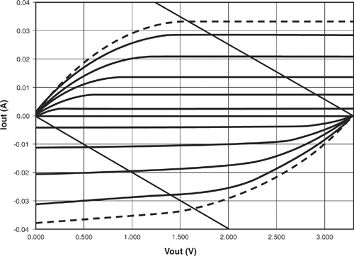
Note that the solid curves in Figure 3.6 correspond to Vgs voltages spaced evenly at 0.5 V intervals beginning at 1.0 V. The threshold of the p-channel transistor is higher than the n-channel transistor, and one of the p-channel curves is flat at zero.
The output IV curves for a driver obey a non-linear relationship that is difficult to quantify. In fact, device physicists have divided the IV space into two regions in which different sets of equations apply.[3] These equations and their derivatives must remain continuous across the boundary between the two regions; if they are not, non-convergence of SPICE simulations will occur, and this never made anybody's day.
Output Impedance
Is it possible to extract any useful information from these curves without running a simulation? Imagine holding the input of the driver in a low state and connecting a resistor between the output and VDDIO. What will the output voltage and current be? An easy way to answer this question graphically is to draw the linear IV characteristic of the resistor on top of the "final" IV curve of the n-channel pull-down transistor—that is, the curve that represents the largest value of Vgs achieved when switching is complete. The intersection of the line and the curve is the operating point of the driver with that particular load. Dividing the voltage by the current gives the output impedance of the driver—at that operating point.
What does output impedance mean, and what is its relevance? If we load the driver with an ideal resistor whose value is the same as the output impedance of the driver, the output voltage will be VDDIO/2 by virtue of the voltage divider equation. If the value of the resistor is the same as the impedance of the transmission line connected to the driver in a system application, the output voltage will be the same as the input to the transmission line when the driver is in the middle of the switching event—that is, before the reflected wave has returned to it. This is a useful thing to know because it is important that the driver be strong enough to deliver the energy it takes to cause a full-swing waveform at the receiver input.
The driver will deliver its maximum power to the load when its impedance is equal to that of the load. Keep in mind that the output impedance of the driver is a function of its load. The IV curve of another resistor will intersect the IV curve of the driver at a different point. Another important point is that there are really two output impedances for a push-pull driver: one for the p-channel devices and one for the n-channel devices. In a well-designed driver, these two impedances will be nearly equal, but this is not always the case. An unbalanced driver can be quite difficult to work with because optimizing the net topology for the rising edge will cause the falling edge to be too strong or too weak.
The dc operating point simulations in Figures 3.7 and 3.8 define another method to extract driver output impedance using the voltage divider equation to calculate the equivalent resistance of the driver given a particular resistive load. This technique is also useful in a transient simulation or in the lab where sweeping the output current of a driver requires special test equipment.
Figure 3.7. Calculation of output high impedance

Figure 3.8. Calculation of output low impedance

Output Rise and Fall Times
Output rise and fall time are, in a sense, a combination of output impedance and capacitance. When a driver switches, it must move charge between its own intrinsic capacitance and the power supply rails. The size of these capacitors and the channel resistance of the transistors govern the rate at which the driver is able to move charge. We can define the intrinsic rise and fall times of the driver as the fastest possible time that a driver can change states when no load is present. The switching time of the pre-drive stage—i.e., the transistors immediately preceding the final output stage—also influences the output rise and fall times. As is the case with output impedance, the rise and fall times may be significantly different if the circuit designer did not intentionally make them the same.
Output rise and fall times have a domino effect on the system design. At a bare minimum, the knee frequency or corner frequency associated with a given rise or fall time determines the bandwidth requirement for all interconnect between the driving and receiving chips.[4] Likewise, it also determines the bandwidth requirements for models used in simulation, and this bandwidth is typically higher than that required for the actual interconnect since simulators must accurately reproduce the corners of waveforms and noise pulses of short duration. The minimum rise or fall time determines the length at which a piece of wire begins behaving like a transmission line.
On the negative side, the instantaneous changes in current that accompany sharp edges produce disturbances on the power distribution system that may ultimately result in the violation of flip-flop setup and hold times. Rapidly changing electric and magnetic fields surrounding a discontinuity such as a connector cause coupling between adjacent signal conductors—another detractor from system performance.
As signal integrity engineers, one of the first tasks we face at the beginning of a new project is cataloging rise and fall times for each bus and each chip, for they will dictate the interconnect technology and models requirements (see Table 1.2). The intrinsic rise and fall times will be misleading, however. The actual rise and fall times measured at a package pin will most certainly be lower as the wave encounters extra capacitance, attenuation from conductor and dielectric losses, and perhaps the inductance of a bond wire array. After passing through the first layers of interconnect, the corners of the waveform will no longer be as sharp.
It is no coincidence that the derivative of a typical digital waveform has a Gaussian-like shape—the same shape as a crosstalk pulse. Coupled noise is a direct function of dV/dt. Cataloging this metric in mV/ns will help you understand where crosstalk hotspots are and how to control them. Be aware that instantaneous dV/dt can vary as much as 30% from a linear estimate using the 20% and 80% crossing points.[5] Lower speed interfaces are not sensitive to this subtlety, but it can make a difference worth paying attention to when you're counting mV. The dV/dt in Figure 3.9 is 9.1 V/ns using the linear approximation; the actual instantaneous dV/dt in Figure 3.10 is 12 V/ns.
Figure 3.9. Edge rate calculated at 20% and 80% points

Figure 3.10. Instantaneous dv/dt

CMOS Current Mode Driver
Most high-speed serial interfaces do not use CMOS push-pull drivers; they use current mode drivers that bear some resemblance to the schematic in Figure 3.11. This is really just the same circuit as the differential receiver in Figure 3.3, except the transistors are much larger and the resistors are in the neighborhood of 50 ![]() .
.
Figure 3.11. CMOS current mode driver

Let's do a quick dc analysis of this circuit. The pre-drive stage drives M1 and M2 differentially, so when M1's channel is conducting, M2's channel is off. The equivalent circuit is Figure 3.12. To get the voltage at the positive output pin, calculate the parallel resistance of R1 combined with R2 + RT. It's 37.5 ![]() , which means the voltage at node P is 750 mV. Because the right branch has three times the resistance as the left branch, it carries ¼ the current or 5 mA. The drop across RT is 500 mV. The mirror analysis applies when M2 is on, and each output swings between 750 mV and 1250 mV for a net differential swing of 1000 mV at the receiver input.
, which means the voltage at node P is 750 mV. Because the right branch has three times the resistance as the left branch, it carries ¼ the current or 5 mA. The drop across RT is 500 mV. The mirror analysis applies when M2 is on, and each output swings between 750 mV and 1250 mV for a net differential swing of 1000 mV at the receiver input.
Figure 3.12. DC analysis of CMOS current mode driver
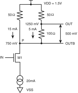
This circuit has some favorable qualities. Ideally, there is no net change in current through the source when the output switches states. If the legs are balanced properly and driven "exactly" out of phase, the net change in current through the VDDIO supply will be zero as well. This means no simultaneous switching noise between VDDIO and VSS on the die and no noise-induced jitter. Well, almost none. If any circuit were ideal, we would all be out of jobs.
The CMOS push-pull driver in Figure 3.5 uses both p-channel and n-channel FETs. In an ideal circuit, both channels would have the same resistance. In real life, the p-channel and n-channel resistances mistrack each other, leading to asymmetrical rise and fall times. The current mode driver solves this problem by using only n-channel transistors.
Behavioral Modeling of IO Circuits
Behavioral modeling has not always enjoyed a good reputation. In the early days of the signal integrity boom, many die-hard proponents of SPICE simulation (myself included) could not understand how such a simple model could accurately reproduce the behavior of dozens of transistors in a complex IO circuit. The complexity of the two models seemed to be different by one or two orders of magnitude. The remarkable fact, however, is how closely a behavioral model does mimic the characteristics of an IO circuit—if certain assumptions are satisfied and if the author of the model did his or her homework.
In hindsight, this should not be too surprising. For all its complexity, the set of device equations that SPICE solves for every instance of a transistor is really a behavioral model, too, albeit a much more complicated behavioral model. The more fundamental equation that describes the behavior of quantum mechanical systems in semiconductors is the Schrödinger Equation, and no one would ever consider using it to simulate transistors. In a sense, every mathematical model of a physical system is a behavioral model. Einstein said we should strive to make these models as simple as possible—but no simpler!
The IO Buffer Information Specification (IBIS) emerged in 1993 with a mission to satisfy the modeling needs of the growing signal integrity community while preserving IO circuit and semiconductor process intellectual property. Today, another urgent need presses the community toward advanced time- and frequency-domain simulation techniques: the need for simulations that will run at all. The combination of advanced CMOS device technologies, lossy transmission lines, s-parameters, and large-scale coupling has rendered an alarming number of SPICE simulations a quivering blob of pudding.
The primary job responsibility of a signal integrity engineer is to ensure the reliability of chip-to-chip interfaces, not to debug models. Time spent resolving non-convergence problems and waiting for multi-day simulations to finish is time wasted. In a more efficient paradigm, we would use behavioral simulation to define the boundaries of the design space, which probably accounts for 80% of all simulations. Then, for the most demanding interfaces, SPICE simulation would provide back-end verification that the behavioral modeling was indeed correct.
IBIS version 1.1 is a natural platform on which to build an understanding of behavioral modeling and simulation of IO circuits. A variety of industry-standard bus technologies are available to signal integrity engineers today: Gunning Transceiver Logic (GTL), High-Speed Transceiver Logic (HSTL), and Stub Series Terminated Logic (SSTL), to name a few of the JEDEC standards. There is an even wider variety of circuit design techniques, some of which are company jewels and may never be known to the world at large. Among the well-known techniques are the simple push-pull driver, open-drain driver, multiple phased output stages, dynamic termination, de-emphasis, equalization, and so on. HSTL and SSTL both use a push-pull output, while classical GTL is an open drain output with a feedback network.
Any behavioral model assumes one of these known circuit design techniques as a template. The information contained in an IBIS model is really not a model at all; the model resides under the hood of the simulator. An IBIS model is merely a database of circuit parameters and tables that a simulator will load into its own unique behavioral model before initiating the simulation. If the circuit template in the simulator does not match the information in the IBIS model, the results of the simulation may not be worth much at all.
Behavioral Model for CMOS Push-Pull Driver
The 50 ![]() CMOS push-pull driver from the previous SPICE simulations will serve as a demonstration vehicle for understanding how behavioral simulation works, how it is different from SPICE simulation of the same circuit, and what its accuracy limitations are. How do the transistor model and the behavioral model compare to one another?
CMOS push-pull driver from the previous SPICE simulations will serve as a demonstration vehicle for understanding how behavioral simulation works, how it is different from SPICE simulation of the same circuit, and what its accuracy limitations are. How do the transistor model and the behavioral model compare to one another?
The p-channel and n-channel transistor symbols in Figure 3.13 represent many parallel transistors that share a common gate, source, and drain. Beneath each of those transistors lies one instance of the device equations that govern the current-voltage behavior of that transistor. The SPICE model statement personalizes the device equations for a particular semiconductor process. In the behavioral model, a single time-dependent voltage-controlled current source (VCCS), whose current-voltage characteristics are defined by a look-up table, replaces all the p-channel transistors in the output stage.
Figure 3.13. Behavioral model for CMOS push-pull driver
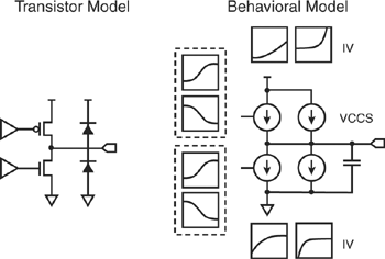
The behavioral simulator ensures that whenever a given current is flowing through the source, the voltage across it will be the same value found in the look-up table for that current. The lower VCCS represents all of the n-channel transistors. Herein lies one of the fundamental assumptions of behavioral modeling: Although SPICE has access to the continuous family of IV curves for any transistor, the behavioral model has only one curve and must make assumptions about what all the other curves in the family look like. This is true for both the n-channel and p-channel devices.
Another fundamental assumption involves the pre-drive stage of the IO circuit, represented in this diagram by the two triangular buffers that independently drive the pull-up and pull-down transistors. (Recall that in the CMOS driver, these were actually NAND and NOR gates rather than simple buffers.) The switching rates of these pre-drive buffers determine the rise and fall times of the output stage, together with the IV curves and loading.
Programs that generate IBIS models do not have access to node voltages that are internal to the driver SPICE subcircuit. This is particularly true if the SPICE subcircuit is encrypted or if the IBIS model was extracted from lab measurements. Therefore, the behavioral simulator must make further assumptions about the rise and fall times at the input of the driver final stage based on rise and fall times of the output.[6]
In the case of an IBIS 1.1 model, the simulator also assumes that the pull-up and pull-down transistors switch at the same time, which is not necessarily the case if the pre-drive stage has two independent buffers. This also is a fundamental assumption. In the diagram of the behavioral model in Figure 3.13, the third terminal on the VCCS represents the time-domain waveform that turns the source on and off, which is analogous to the Vgs waveform at the input of the final stage in a SPICE driver subcircuit.
There are two sets of voltage-time waveforms to the left of the VCCS enclosed by dashed boxes. One set of waveforms controls the pull-up transistors, and the other controls the pull-down transistors. In IBIS 1.1, both sets of waveforms begin switching at the same time. IBIS 2.1 allows independent control over the pull-up and pull-down transistors via a set of voltage-time waveforms rather than a simple rise and fall time.
The second set of voltage-controlled current sources corresponds to the two ESD protection devices. Compared to the complexity of the pull-up and pull-down elements, these seem trivial as they have no time-dependent waveform turning them on and off. Each VCCS draws current from its corresponding supply rail. If the circuit were a receiver with some form of on-die termination, the IV curves for the termination would be superimposed on top of the ESD curves.
Finally, the lumped capacitor, called C_comp in IBIS, represents all capacitances that are connected to the output node of the circuit: transistors, ESD protection diodes, metal, and bond pad or solder ball. The value of this capacitor is not a function of time or voltage, which is a good assumption if the semiconductor junctions are reverse biased (see Equation A.1). As soon as they begin to conduct this assumption breaks down.
The physical location of C_comp may also be relevant. Drivers with on-chip series termination will have their capacitance distributed on either side of the resistor, and this can become an accuracy issue. In simultaneous switching simulations, the assumption that the other node of the capacitor is connected to ground breaks down.[7] In the case of the CMOS driver, however, a constant lumped C_comp remains a valid assumption.
Behavioral Modeling Assumptions
In summary, the fundamental assumptions for an IBIS 1.1-compatible behavioral model of the CMOS driver are as follows:
- The behavioral model topology that the simulator employs is consistent with the IO circuit design (in this case, a simple CMOS push-pull final output stage).
- The behavioral simulator interpolates between a single pull-up (p-channel) IV curve and a single pull-down (n-channel) IV curve.
- The behavioral simulator infers the Vgs waveform at the input to the final stage from the rise and fall times measured at the output of the final stage with a 50
 load.
load. - The pull-up and pull-down transistors begin switching at the same time.
- A single constant-value capacitor represents all capacitances seen looking into the pad node.
Tour of an IBIS Model
Armed with an understanding of the IO circuit models used in signal integrity simulations, you can confidently assess the quality and accuracy of the models needed to perform your own analysis of the timing and voltage margins for a given interface. Model assessment is a significant step toward engineering a reliable digital interface.
A close look at an example IBIS model points out the differences and similarities between a behavioral model and a SPICE transistor model. The data structures within this IBIS model file illustrate the assumptions a behavioral simulator makes about the electrical characteristics of an IO circuit and how those assumptions compare to a SPICE model of the same circuit. The IBIS Committee has published a good deal of educational material, including instructions on how to create IBIS models.[8]
There are three main sections to this simple IBIS model: the header, the pin table, and the model data. IBIS is fundamentally a chip-centric specification, so there is a one-to-one correspondence between an IBIS model and the chip it represents. There are some cases when a chip manufacturer may publish a library of individual models from which the user can assemble a complete IBIS model—for example, ASIC development.
The header contains various bits of background information about the file. The pin table lists each pin in the chip and, if the pin is a signal, associates a model with it. In the language of IBIS, keywords are enclosed in brackets, [ ], and may be followed by sub-parameters that are associated with the preceding keyword. For example, the [Model] keyword defines a new set of IO circuit model parameters, including pin capacitance, rise and fall times, and IV curves. The "Model Type" sub-parameter is hierarchically below the [Model] keyword, and it can take on the values Input, Output, I/O, 3-state, or Open_drain. The [Model] keyword covers the first assumption of behavioral modeling: It defines the circuit topology that the simulator will use.
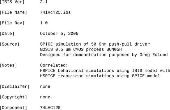


IBIS Header
The header stores some valuable information. The version keyword allows the syntax checker to decide which features are legal. The file name keyword and the actual name of the file must match one another. This file happens to represent a fictional low-voltage CMOS (LVC) dual tri-state buffer in a standard 125 form factor that uses the CMOS push-pull driver circuit, drv50.
The source, notes, and disclaimer keywords are of special interest. A conscientious author will give some indication of the conditions under which he or she created the IBIS model. Did the information come from production-level SPICE models that were extracted from an integrated circuit layout? Or perhaps the source was lab measurements of an actual component, which only apply to one process-temperature-Voltage point. If the author's name does not appear under the source keyword, the user might wonder whether anyone is willing to support the IBIS model.
Many signal integrity engineers find this common disclaimer to be particularly disturbing: "...for modeling purposes only." This seems to suggest that the vendor does not stand behind the IBIS model in the same way it stands behind the component datasheet. This is disconcerting because model parameters are in some ways even more influential in determining the success or failure of a design than the simpler parameters found in a component datasheet. However, if the quality of an IBIS model is not consistent with the needs of the design, signal integrity engineers have a tool for affecting change that is more potent than complaining: Include model quality and accuracy in the purchase order.
IBIS Pin Table
The pin table, designated by the [Pin] keyword, associates a [Model] keyword with a chip pin number. Remember, the information found in an IBIS model is not really the model itself but rather the input parameters to the model; the model resides inside the simulator. The language can be a bit confusing on this point. The first two columns in the table store the pin number and name as found in the component datasheet. If the user is running automated post-route simulation, the software will match the pin number in the logical netlist with a pin number from this table. Every model name found in the third column must have a matching [Model] keyword under the model section of the datasheet. The remaining three columns contain lumped RLC parameters for the purpose of modeling the package pin.
There are three ways to code IC package model data in IBIS. If the optional per-pin parameters do not exist under the pin table, the simulator assigns the default values found under the [Package] keyword to every pin. IBIS 2.1 offers a more sophisticated means of coding package models using the [Define Package Model] keyword. In the following example, the model for pin 10 of a BGA package comprises three sections: a 2 nH lumped inductance for the bond wire, a 0.5 in length of 50 ![]() transmission line for the copper wire, and a 1 pF lumped capacitance for the solder ball and pad. In this case, the information truly does define a circuit-based model for the package; there is no ambiguity left for the simulator to resolve.
transmission line for the copper wire, and a 1 pF lumped capacitance for the solder ball and pad. In this case, the information truly does define a circuit-based model for the package; there is no ambiguity left for the simulator to resolve.
|
10 Len=0 L=2nH / Len=0.5 C=3pF L=9nH R=1m / Len=0 C=1pF /
|
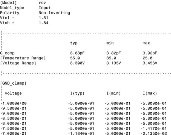
IBIS Receiver Model
The first set of model data following the pin table corresponds to the receiver circuit, rcv. The previous section on IO circuit characteristics discussed three primary attributes of a simple CMOS receiver, and each has its place in the IBIS receiver model: threshold voltages, pin capacitance, and IV curves. Most IBIS models for low-voltage CMOS (3.3 V) use the default TTL thresholds commonly found in component datasheets—that is, 0.8V and 2.0V. I extracted the thresholds for this IBIS model from SPICE simulations of the receiver circuit, which means they are more accurate and result in less conservatism in the system design.
The [Temperature Range] and [Voltage Range] keywords document the conditions under which the model author derived the other keywords and sub-parameters. Some degree of confusion has surrounded these keywords because the values found under the min column are not always the smallest numerical values, and the values found under the max column are not always the largest. The values found under the min column for the [Temperature Range] and [Voltage Range] keywords correspond to the conditions that gave the highest channel resistance, also called weak, slow, or worst, depending on convention at your place of employment. For a CMOS process, high temperature and low voltage go along with weak silicon, and these conditions are the ones that produced the IV curves found in the min column of the [GND_clamp] and [POWER_clamp] keywords. Conversely, the values found under the max column for the [Temperature Range] and [Voltage Range] keywords represent the simulation conditions that gave low channel resistance, also called strong, fast, or best.
The confusion arises in two places. First, the min value of the [Temperature Range] keyword is the highest temperature for CMOS chips. Min really refers to current. Second, the C_comp sub-parameter does not obey the rules described in the previous paragraph! The min value for C_comp should be the smallest numerical value, and the max value should be the largest numerical value—regardless of the process, temperature, and voltage conditions.
The [GND_clamp] keyword stores the IV curves for the current that flows in through the pad node and out through the VSS node. In the CMOS receiver circuit, the current flows only through the ESD protection devices; the input to the buffer is two high-impedance MOSFET gates that draw very little current. In more sophisticated receivers, current may also flow through passive or active termination devices, usually transistors.
The [POWER_clamp] keyword stores the IV curves for the current that flows in through the VDDIO node and out through the pad node. According to the current convention in IBIS, negative currents flow into the pad node and positive currents flow out. Another important IBIS convention: the voltages in the [POWER_clamp] tables are referenced to VDDIO rather than VSS. Because this is a CMOS circuit whose VDDIO rail is 3.3V, this means that the first column in the table reads -3.3V when the actual input is at ground and 0V when the input is at VDDIO! This feature allows the simulator to change VDDIO voltages without having to recalculate the IV curves.
In this IBIS receiver model, the voltage-controlled current sources in the corresponding behavioral model are always in an active state. Some receiver circuits activate their termination devices dynamically; special syntactical constructs in IBIS 3.2 facilitate modeling these circuits.
IBIS Driver Model
Compare the first few lines of code immediately following the drv50 and rcv [Model] keywords; the only difference is that the sub-parameters Vmeas, Cref, Vref have replaced the sub-parameters Vinl and Vinh. The model for a tri-state driver does not need receiver switching thresholds, but it does require a description of the standard load found in the component datasheet. During automated post-route simulation, the simulator will load drv50 with Cref, measure the time at which the package pin node crosses Vmeas, and store this value for later use as time zero in all timing calculations. If you are extracting interconnect timing from post-route simulations, it is critical that these values exactly match those in the component datasheet.
The code under the drv50 [Model] keyword contains the same [GND_clamp] and [POWER_clamp] tables found under the rcv [Model] keyword because these IV curves represent the ESD protection devices, which are the same for both IO circuits. The two keywords [Pulldown] and [Pullup] are unique to drivers, and they store the IV curves for the n-channel and p-channel transistors in the output stage of this simple CMOS push-pull driver. Like the [POWER_clamp] table, the [Pullup] table is also referenced to VDDIO.
Extracting the [Pulldown] and [Pullup] tables for a driver is not as simple as extracting the [GND_clamp] and [POWER_clamp] tables for a receiver because the transistor IV curves and the ESD device IV curves are embedded in the same set of curves—unless the author manually edits the SPICE subckt for the driver and comments out the ESD devices. The common solution to this problem is to disable the driver, measure the ESD device IV curves, and subtract them from the composite IV curves to get the [Pulldown] and [Pullup] tables. This procedure is the source of the non-monotonic warnings IBIS users often see when they run ibischk. The SPICE model for a diode contains an exponential equation, which can generate huge differences in current for very small changes in voltage:

Subtracting one huge number from another huge number causes round-off error in the less significant digits. These errors are usually innocuous and do not have a significant effect on simulation results; simulators and users usually ignore them. However, they do have the potential to generate a large number of warning messages that need to be sorted.
The one remaining piece of information needed to make a behavioral driver model work is how fast the [Pulldown] and [Pullup] tables transition from an off state to an active state. In an IBIS 1.1 datasheet, the [Ramp] keyword stores this information, which is simply Δt and ΔV measured at the 20% and 80% points when the driver is loaded with R_load, which is usually 50 ![]() to VSSIO for a rising edge and 50
to VSSIO for a rising edge and 50 ![]() to VDDIO for a falling edge. The 20% and 80% points are a fraction of the output swing rather than VDDIO.
to VDDIO for a falling edge. The 20% and 80% points are a fraction of the output swing rather than VDDIO.
From this information, the behavioral simulator constructs an "internal stimulus function" that activates the [Pullup] table while deactivating the [Pulldown] table in the case of a rising edge. It also has to account for the fact that the [Ramp] values were extracted in the presence of C_comp, the pin capacitance. The behavioral simulator must be able to correctly replicate the values in the [Ramp] table when loaded with R_load.
Not as simple as it appears at first glance!
Behavioral Modeling Assumptions (Reprise)
It is now possible to restate the fundamental assumptions of behavioral modeling cast in the language of IBIS 1.1, as follows:
- The behavioral simulator assumes the IO circuit topology to be one of the following forms: Input, Output, I/O, 3-state, or Open_drain.
- The behavioral simulator interpolates between the [Pullup] table and the [Pulldown] table to find the trajectory of the driver output through IV space during the switching event.
- The behavioral simulator constructs an internal driving function from the rise and fall times measured with a 50 load and uses this function to turn the [Pullup] and [Pulldown] tables on and off.
- The [Pullup] and [Pulldown] tables begin switching at the same time.
- C_comp represents all capacitances seen looking into the pad node.
It is extremely important to understand that the behavioral simulator has no information about anything that happens prior to the driver output stage or after the receiver input. This implies that the concept of IO circuit delay has no meaning in an IBIS-based behavioral model. It also implies that all timing constraints associated with storage elements inside the chip reside elsewhere!
In a behavioral model based on IBIS 1.1 assumptions, the [Pulldown] and [Pullup] tables begin switching at the same point in time even though this may not be the case in a real-life IO circuit. The circuit designer may have intentionally skewed the turn-on of the p-channel devices from the turn-off of the n-channel devices to prevent a temporary short circuit between VDDIO and VSS. This current does nothing useful and generates di/dt noise. To enable modeling of non-linear skewed internal driving functions, IBIS 2.1 implemented a feature known as VT tables, which look like this:

Like the [Ramp] keyword, there is a sub-parameter, R_fixture, in the VT table that specifies the load resistance. Unlike the [Ramp] keyword, the termination voltage of the R_fixture is not assumed; the V_fixture sub-parameter defines the termination voltage. Another difference is that two rising waveforms replace the single dV/dt quotient: one for 50 ![]() to VSS, and one for 50
to VSS, and one for 50 ![]() to VDDIO. The same is true for the falling edge. With more complicated information at its disposal, the behavioral simulator is able to construct a more realistic internal stimulus function, which results in a better match between behavioral and transistor simulation results—at least for loads close to R_fixture.
to VDDIO. The same is true for the falling edge. With more complicated information at its disposal, the behavioral simulator is able to construct a more realistic internal stimulus function, which results in a better match between behavioral and transistor simulation results—at least for loads close to R_fixture.
Comparison of SPICE and IBIS Models
The most obvious difference between these two kinds of models is that there are many fewer lines of code in the drv50 SPICE subckt than there are under the corresponding IBIS [Model] keyword. This is not always the case, since some SPICE models have hundreds of transistor model calls and a plethora of resistors and capacitors that model the wires between transistors. The reason for the apparent simplicity of the SPICE model for this demonstration circuit is that most of the complexity is hidden in the transistor model equations, one instance of which is called every time a transistor appears in the subckt. SPICE calculates the terminal currents and voltages of every transistor rather than relying on tables to calculate only the pad node voltage and the currents flowing in and out of the pad node.
*---------------------------------------------------------------------*
* a en pad vss vdd vssio vddio
.subckt drv50 10 20 30 100 200 1000 2000
*---------------------------------------------------------------------*
xnand 10 20 40 100 200 drvnand
xnor 10 60 50 100 200 drvnor
xinv 20 60 100 200 inv
mpout01 30 40 2000 2000 cmosp l=0.5u w=20.0u
mpout02 30 40 2000 2000 cmosp l=0.5u w=20.0u
mpout03 30 40 2000 2000 cmosp l=0.5u w=20.0u
mpout04 30 40 2000 2000 cmosp l=0.5u w=20.0u
mpout05 30 40 2000 2000 cmosp l=0.5u w=20.0u
mpout06 30 40 2000 2000 cmosp l=0.5u w=20.0u
mpout07 30 40 2000 2000 cmosp l=0.5u w=20.0u
mpout08 30 40 2000 2000 cmosp l=0.5u w=20.0u
mpout09 30 40 2000 2000 cmosp l=0.5u w=20.0u
mpout10 30 40 2000 2000 cmosp l=0.5u w=20.0u
mpout11 30 40 2000 2000 cmosp l=0.5u w=20.0u
mnout01 30 50 1000 1000 cmosn l=0.5u w=20.0u
mnout02 30 50 1000 1000 cmosn l=0.5u w=20.0u
mnout03 30 50 1000 1000 cmosn l=0.5u w=20.0u
mnout04 30 50 1000 1000 cmosn l=0.5u w=15.0u
desd1 1000 30 esd area=200
desd2 30 2000 esd area=200
cpad 30 0 1pF
.ends
The SPICE subckt contains circuit topology and connectivity information, while the IBIS model only makes reference to a pre-defined IO circuit type. IBIS depends on the behavioral simulator to define the circuit topology and load the corresponding model with the information from the IBIS model. Although IBIS covers the majority of IO circuits, some circuits employ more complex topologies and functions that do not fall under the umbrella of predefined IBIS model types.
One example is a driver that employs de-emphasis, a technique used to combat attenuation and inter-symbol interference. In this type of driver, the output impedance is a function of the data pattern history. When driving two zeros and then a one, the output impedance is stronger than it would be when driving one zero and then a one (see Chapter 7, "PCI Express Case Study"). Although IBIS 4.1 does not include a predefined model type for de-emphasis, it does allow the user to call external models written in other languages that may facilitate modeling of this and other circuits. The user must be aware that a behavioral simulation may not faithfully reproduce the waveforms you would expect to see in a SPICE simulation of the same circuit. So how is the user to know whether or not to trust the output of a behavioral simulator? This question leads into the multi-faceted topic of simulation accuracy.
Accuracy and Quality of IO Circuit Models
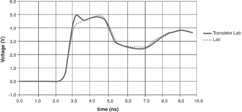
There are many factors that muddy the waters around the issue of accuracy; a simple working definition for engineers adds some clarity. The accuracy of a simulation is a measure of how close the simulation results come to lab measurements. Lab data are not easy to come by. Although it may be possible to characterize an IO circuit on a simple buffer chip in the lab, getting an output to switch on a microprocessor or a DRAM requires a live system, software, and a diagnostics console. Hopefully the circuit designer spent the time to correlate lab measurements on prototype silicon with SPICE simulations during the design verification process. Figure 3.14 is a clear graphical representation of model-to-hardware correlation. For complex IO circuits found in high-performance interfaces, it is entirely appropriate for a signal integrity engineer to request proof of accuracy from the chip vendor.
Figure 3.14. Correlation of transistor-level simulation to lab data
What about the other IO circuits that get used in mid-range and low-end applications and account for a majority of all silicon in production today? Is it reasonable to request rigorous proof of accuracy to a 10% tolerance on all these circuits? Probably not, since operating margins are not tight enough to justify the expense associated with the extra effort. In the end, we must rely on the process the semiconductor manufacturer implements to model transistors and the process the chip designer implements to extract transistor-level models from IO circuit layout data.
If the model data take the form of an IBIS model or some other behavioral format, a secondary question persists: how well does the behavioral simulation agree with the transistor-level simulation? This question also touches on the topic of accuracy, though it is one level removed from lab measurements. If the behavioral simulation agrees with the transistor-level simulation which in turn agrees with the lab, then the behavioral simulation is accurate by proxy.
Much debate has surrounded the topic of behavioral model accuracy, the perspectives ranging all the way from behavioral models being useless to behavioral models being sufficient to design multi-gigabit interfaces. Reliable studies have demonstrated close agreement between behavioral simulation results and transistor-level simulation results (see Figure 3.15) across a wide range of operating conditions subject to two caveats.
Figure 3.15. Correlation of transistor-level and behavioral simulation

First, the topology of the behavioral model must mirror the topology of the actual IO circuit. If the driver has three parallel multi-phased output stages but the behavioral model has only one, the accuracy may be less than acceptable. Second, the engineer who builds the behavioral model must understand the IO circuit. If that engineer merely runs a translator without bothering to find out how the circuit works or without checking the results, then simulations that use that behavioral model are unlikely to be accurate. Both these caveats imply that the end user is entirely dependent on the chip designer since it is unlikely that the end user will ever see a circuit schematic.
How can someone with little or no access to information about an IO circuit feel confident in the results of a simulation that uses a behavioral model derived from an IBIS model? Fortunately, IBIS version 4.1 has a little-known mechanism for bundling a set of "Golden Waveforms" together with the normal model parameters and tables found in an IBIS model. The model builder can include waveforms for a combination of realistic loads such as a transmission line, termination network, and pi network. The user can simulate the behavioral model under the same loading conditions and then overlay results on top of the Golden Waveforms. In an ideal world, the simulator would do this automatically and report the results to the user.
The [Test Data] keyword marks the beginning of the Golden Waveforms, and the [Test Load] keyword describes the network corresponding to the measurement or simulation conditions that produced the waveforms. The [Test Load] keyword allows the model builder to select any combination of the elements from the template in Figure 3.16.
Figure 3.16. Golden Waveform test load

When comparing transistor-level and behavioral simulation results, be aware that different behavioral simulation engines may produce different results for the same IBIS model and the same test load. Even though the input data are the same, the algorithms for translating the data, constructing an equivalent circuit, and solving that circuit vary from simulator to simulator. The package model is another significant factor that may cause more correlation trouble than the IO circuit itself. Correlating with and without the package model can shed light on the source of the discrepancy.
Of course, the preceding discussion assumes that the models will run in the first place. The entire issue of accuracy becomes a moot point if there are fundamental syntactical errors that prevent the simulator from ever running. Both SPICE and IBIS models are susceptible to general quality issues. SPICE models are particularly susceptible to numerical issues embedded deep within the transistor model parameters. They may also be missing fast or slow transistor model parameters. IBIS models may likewise be missing min or max tables and sub-parameters. Sometimes an IBIS file doesn't even pass the syntax checker, which leads the user to question everything else in the file! Lack of documentation is a generalized problem that is endemic to both types of models. The IBIS Committee has published a quality checklist of errors commonly seen in IBIS models, as well as a few errors pertaining to SPICE models.[9]
In the face of all that can go wrong with the IO circuit modeling process, signal integrity engineers understandably feel vulnerable because the success of our designs depends so strongly on models developed by people who don't share the same motivations. However, consumers of electrical component models hold one powerful tool that is seldom used. If model quality and accuracy are truly important to the company purchasing the chips, then that company can work with their vendors to make model quality and accuracy part of the purchasing agreement.