
2.6 Principles of Modeling of Slow-Wave Structures
Modeling of electrodynamic slow-wave systems using the multiconductor line method consists of several steps:
1. The multiconductor line with the cross-section shape and dimension that are the same as in the MCL is used in the model.
2. The segment of the MCL of length (in x direction) corresponding to the length of conductors in the real system is considered (Figure 2.6).
3. Boundary conditions are applied. In the general case, loads with impedances Z_+n+i and Z_−n+i
4. Equations describing relationships between voltages and currents at the ends of conductors are constructed. At N conductors in a period, the set consists of 2N equations. The set of equations is the mathematical model of the slow-wave system.

FIGURE 2.6
Generalized model of a slow-wave system. 1: Conductor of the MCL; 2: shield; 3: dielectric layer with permittivity ε.n Z_+n+i and Z_−n+i:
In the case of the model presented in Figure 2.6, the set of equations is
The set contains 2N unknown coefficients (Av and Bv), unknown phase angle θν, and wave frequency ω.
Solving the set of equations, we can find relationships between coefficients Av and Bv. Values of these coefficients are dependent on the level of the electromagnetic wave excited in the system.
Finally, we can eliminate coefficients Av and Bv and derive the dispersion equation containing unknown variables θv and ψ:
(2.138) |
Solving this equation, we can plot the dispersion characteristic of the slow-wave system.
Equation (2.138) contains phase angle θv as a variable. Additionally, wave impedances and effective dielectric permittivity depend on θv. Thus, the more detailed expression of the dispersion equation is of the following form:
(2.139) |
In practice, numerical methods are used for solution of the dispersion equation.
At known solutions of the derived dispersion equation, taking into account relationships between coefficients Av and Bv it is possible to find characteristic impedance and input impedance versus frequency.
The characteristic impedance is given by
(2.140) |
where U(−jβz) and I(−jβz) are the complex amplitudes of the voltage and current of waves propagating in the z direction.
In practice, slow-wave systems usually are nonhomogeneous structures. Then the calculation of characteristic impedance is complicated, and input impedance is used as the most important parameter when problems related to matching of the system with signal path are solved.
The input impedance is given by
(2.141) |
where Un(x) and In(x) are complex voltage and current amplitudes at the section x of the nth conductor in the period.
According to Equation (2.141), in the general case, the input impedance is dependent on the number of conductors, on coordinate x, and, of course, on frequency.
Finally, it is important to notice that calculations of characteristic admittances of conductors and calculation of effective dielectric permittivity must precede solution of the dispersion equation and calculation of the input impedance of the system.
Thus, after a mathematical model of the slow-wave system is designed, analysis of frequency properties of a slow-wave system contains these steps:
1. Calculation of characteristic admittances of conductors and effective dielectric permittivity at selected values of the phase angle θ.
2. Solution of the dispersion equation at selected values of the phase angle θ using numerical iterations. Calculation of the retardation factor at determined values of the phase angle θ and frequency ω.
3. Calculation of input impedance at determined values of frequency ω.
2.7. Application of the Multiconductor Line Method for Analysis of Nonhomogeneous Systems
In order to illustrate application of the multiconductor line method for analysis of nonhomogeneous systems, let us consider axially symmetrical meander systems. The view of the cross section of a system is presented in Figure 2.7(a). The system consists of meander electrodes and shields and it can be used for deflection of electron beams in traveling-wave cathode-ray tubes. In order to have high characteristic impedance, peripheral parts are bent to increase the distance between them. Glass rods are used for holding the meander electrodes. Sticks of meander electrodes are plunged into the glass rods (Figure 2.7b). Due to the holding elements, parasitic capacitances appear between the neighboring parts of the meander electrodes (Figure 2.7c).

FIGURE 2.7
(a) The cross section of the meander system, (b) a fragment illustrating sticks of meander electrodes plunged into glass rods, and (c) parasitic capacitances in the system. 1: Meander electrode; 2: shield; 3: glass rod; 4: stick of the electrode.
In super-wide-band deflecting systems, the distance between meander electrodes usually is small. Then, no more than two dielectrical holders are necessary, and the structure of the system is simpler (Figure 2.8a). However, parasitic capacitances arise between the peripheral parts of the electrodes in this instance (Figure 2.8b).
Two types of meander systems are used in practice: systems with plane symmetry and systems with axial symmetry. Analysis of meander systems containing meander electrodes that are symmetrical with respect to the central plane is performed in [2.2]. Now let us consider the system containing elements that are symmetrical with respect to the central axis. Figure 2.8(b) illustrates the positions of the meander electrodes in the system with axial symmetry.
Modeling principles of complex nonhomogeneous systems have been developed by Staras et al. [2]. Let us use these principles for modeling and simulation of the meander system with axial symmetry in order to reveal the influence of holding elements (capacitances C1 and C2) on properties of the system.

FIGURE 2.8
(a) The cross section of the wide-band meander system and (b) fragments of meander electrodes with parasitic capacitances. 1 and 2: Meander electrodes; 3: dielectric rod.
The model of the system for analysis of its properties using the MCL method is presented in Figure 2.9. The segments of the two-row MCLs containing two conductors in a period are used in the model (Figure 2.9a, b). Models of upper and lower meander electrodes are presented in Figure 2.9(c, d). Let us assume that different dielectrics fill the cross section of the system. Let us denote dielectric permittivities of dielectrics in the space between meander electrodes, in the space among the conductors of meander electrodes, and in the space between the electrodes and the shields by εri,ε′ri, and ε"ri,
If the electromagnetic wave in the system is excited by signals with the same amplitudes and opposite polarities, conditions
(2.142) |
(2.143) |
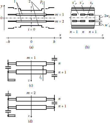
FIGURE 2.9
(a, b) The sections of the model of the meander system with axial symmetry and (c, d) models of meander electrodes with parasitic capacitances. 1: Meander electrodes; 2: shields.
are satisfied, and voltage and current on conductors of the MCL in the central section of the model (i = 0) are given by [3]
U_01n(x)=(B_02cosk0x+(−1)nD_01sink*0x)e−jnθ |
(2.144) |
I_01n(x)=j(−ϒ0ε(π,θ)B_02sin k0x+(−1)nϒ0ε(0,θ+π)D_01cos k*0x)e−jnθ. |
(2.145) |
At i > 0,
U_01n(x)=((B_i1sinkix+B_i2cos kix)+(−1)n(D_i1sin k*ix+D_i2cos k*ix)e−jnθ |
(2.146) |
I_01n(x)=j(ϒiε(π,θ)(B_i1cos kix−B_i2sin kix)+(−1)nϒiε(0,θ+π)(D_i1cosk*ix−D_i2sin k*ix)e−jnθ. |
(2.147) |
In Equations (2.144),(2.145),(2.146),(2.147), B and D are coefficients, i is the number of the section of the multiconductor line, m is the number of the row of the line, and n is the number of the conductor in a row:
(2.148) |
ϒiε(π,θ)=c0√Ciε(π,θ)/Ci(π,θ); |
(2.149) |
k*i=k√Ciε(0,θ+π)/Ci(0,θ+π); |
(2.150) |
ϒiε(0,θ+π)=c0√Ciε(0,θ+π)/Ci(0,θ+π); |
(2.151) |
k = ω/c0 is the wave number
ω = 2πf, f frequency
c0 is the velocity of the electromagnetic wave in the free space
Ciε, (0, ε) is the capacitance of the conductor of the MCL at electrical wall inserted at y = 0
εri=ε′ri=ε"ri=1
Ciε (0,θ+π) is the capacitance of the conductor of the MCL at magnetic wall inserted at y = 0
εri=ε′ri=ε"ri=1
Yiε(π, 0) and Yiε(π, θ + π) are characteristic admittances
x is the coordinate
At the junctions of the segments of MCLs, the boundary conditions
(2.152) |
and
(2.153) |
must be satisfied.
The row m = 1 of the MCL models the meander electrode if these boundary conditions are satisfied:
(2.154) |
Here, r is the number of the peripheral segment of the MCL; xr = h.
After substitution of expressions of voltages and currents in Equations (2.144),(2.145),(2.146),(2.147) into Equations (2.152),(2.153),(2.154),(2.155), we obtain the set of algebraic equations that is the mathematical model of the system.
2.7.2 Dispersion Equation, Retardation Factor, and Input Impedance
Eliminating coefficients B and D from the set of equations, we can derive the dispersion equation. It is not easy to do this when the number of segments is relatively great. The problem can be simplified using matrix algebra, as Staras et al. [2] have done. The dispersion equation obtained using this method is given by [13]
Here,
(2.157) |
(2.158) |
and q and q* are elements of matrices Q and Q*:
Q=P−1r(r−1)P(r−1)(r−1)…..P−121P11P−110R; |
(2.159) |
Q*=P*−1r(r−1)P*(r−1)(r−1)…..P*−121P*11P*−110R*; |
(2.160) |
Pij=(sinkixjcoskixjϒiε(π,θ)coskixj−ϒiε(π,θ)sinkixj); |
(2.161) |
P*ij=(sink*ixjcosk*ixjϒiε(0,θ+π)cosk*ixj−ϒiε(0,θ+π)sink*ixj); |
(2.162) |
R=(cosk0x00−ϒ0ε(π,θ)cosk0x00); |
(2.163) |
R*=(0cosk*0x00−ϒ0ε(0,θ+π)cosk*0x0). |
(2.164) |
Using numerical iterations to solve Equation (2.156), we can find values of the wave constant k corresponding to the selected values of phase angle θ. Then, we can find values of the retardation factor and frequency using the following equations:
(2.165) |
where L is the step of conductors in the meander system and in its model.
The input impedance is dependent on coordinate x. At x = 0, it is given by
ZIN=U_011(0)I_011(0)=1ϒε0(0,θ+π)q*12sink*rxr+q*22cosk*rxrq11sinkrxr+q21coskrxr. |
(2.166) |
Characteristics presented in Figure 2.10 illustrate the influence of capacitances C1 and C2 on the frequency properties of an axially symmetrical meander system. According to Figure 2.10, the retardation factor and input impedance in the low-frequency range do not depend on capacitance C1 because potentials of the sticks (Figure 2.7b) are practically the same and current does not flow through capacitance C1. If frequency increases, the phase difference between voltages on neighboring sticks increases, and capacitance C1 causes increase of the retardation factor and decrease of input impedance as a result of increase of effective capacitances of meander electrodes per unit of length.
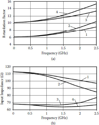
FIGURE 2.10
(a) Retardation factor and (b) input impedance of axially symmetrical meander system versus frequency at L = 2, p = 0.25, εir, = ε′ir = ε″ir = 1, x0 = 2.5, w0 = w′0 = 0.5, x1 = 5, w1 = w′1, = 1, x2 = 7.5, w2 = 1, w′2 = 1.5, x3 = 10, w2 = 1, w′2 = 2 mm. 1: C1 = C2 = 0; 2: C2 = 0.05, C2 = 0; 3: C1 = 0, C2 = 0.05; 4: C1 = C2 = 0.05pF.
At opposite polarities of voltages on meander electrodes, capacitances C2 cause increase of effective capacitances of meander electrodes per unit of length. This is followed by increase of the retardation factor and input impedance in the wide-frequency range.
At C1 ≠ 0 and C2 ≠ 0, capacitances C2 also cause increase of the retardation factor and decrease of input impedance in the wide-frequency range. Capacitances C1 cause increase of the retardation factor and decrease of input impedance at high frequencies.
2.8 Calculations of Frequency Characteristics Using Numerical Iterations
It was mentioned in Section 2.6 that analysis of slow-wave structures consists of several steps when the multiconductor method is used. In analysis of nonhomogeneous systems, the set of equations (mathematical model of the system) consists of many equations. Then, derivation of the dispersion equation is complicated even when the methods of matrix algebra are used.
We can avoid the tedious work necessary for derivation of analytical expression of the dispersion equation using numerical methods [15,16,17] for solution of the set of equations describing the model of the system.
Initially, we will apply a numerical method for analysis of the complex model of a helical system with plane symmetry in this section. After verification of the developed numerical method, we will use it for investigation of the axially symmetrical helical system.
2.8.1 Calculation of Characteristics Avoiding Derivation of Dispersion Equations
The view of the cross section of the helical system consisting of elements that are symmetrical with respect to the central plane is shown in Figure 2.11(a).
Propagation of the even mode in the system does not change if the magnetic wall is inserted in the symmetry plane, and the electric wall in the symmetry plane does not cause any changes at propagation of the odd wave. Thus, the asymmetrical models shown in Figure 2.11(b, c) can be used for analysis of propagation of the even and odd modes.
The odd mode is used for deflection of the electron beam in traveling-wave cathode-ray tubes. Thus, in order to reveal properties of the helical deflection system with plane symmetry, we can examine the asymmetrical system shown in Figure 2.11(b).
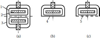
FIGURE 2.11
(a) The cross section of the helical system with plane symmetry and its models for (b) odd and (c) even modes. 1: Helix; 2 and 3: shields; 4: electric wall; 5: magnetic wall.

FIGURE 2.12
(a) The cross section of asymmetrical helical system and (b) the model of the system. 1: Helix; 2 and 3: shields; 4: dielectric holder; 5: conductor of the MCL modeling helix.
The generalized cross-section view of the asymmetrical helical system and its model consisting of segments of MCLs are presented in Figure 2.12(a, b). Dimensions of conductors and distances of shields and dielectric materials in the space among conductors in the segments of MCLs can be distinct.
The one-row MCLs with one conductor in the period are used in sections 11, 12, 31,…52, 71, and 11 of the model. Then, expressions for voltages and currents on conductors are given by [2]
U_imn(x)=(A_im,1sinkimx+A_im,2coskimx)e−jnθ, |
(2.167) |
I_imn(x)=jϒimε(A_im,1coskimx−A_im,2sinkimx)e−jnθ, |
(2.168) |
where i is the number of the segment, m is the number of the row in the model, and n is the number of the conductor in the row.
Sections 2 and 6 in Figure 2.12(b) model the flat parts of the helical system where coupling between parts of the helical conductors is possible because of the limited width of the internal shield. The two-row MCLs with one conductor in a period are used in sections 2 and 6, and voltages and currents on conductors are given by [2]
U_imn(x)=[−(−1)m(B_i,1sinkix+B_i,2coskix)+(B_*i,1sin kix+B_*i,2coskix)]e−jnθ, |
(2.169) |
At the junctions of sections, voltages and currents cannot change. Thus, the structure presented in Figure 2.12 models the helical system if these boundary conditions are satisfied:
where xj denotes the coordinate (Figure 2.12b).
Substituting Expressions (2.167)–(2.170) for voltages and currents into Equation (2.171), we arrive at the set of 28 equations containing 28 unknown amplitude coefficients and two additional variables k and θ. Then the relationship between k and θ can be found considering the matrix with elements that are multipliers of amplitude coefficients in the set of equations. The value of k corresponds to a selected value of θ at zero determinant of the matrix.
Based on numerical iterations, the algorithm for calculation of the retardation factor and input impedance is presented in Figure 2.13. According to it, at a selected value of phase angle θ, characteristic admittances of segments of MCLs in the model and values of effective dielectric permittivity are found. After that, the value of the wave coefficient is found using numerical iterations. Then, after calculation of input impedance, calculations are repeated at a new value of phase angle θ.
At known values of θ and k, values of the retardation factor, input impedance, and frequency are found using the following equations:
(2.172) |
Z_IN(0)=U_12n(0)I_12n(0)=j1ϒ11εA_11,2A_11,1, |
(2.173) |
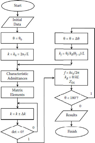
FIGURE 2.13
Algorithm for calculations of characteristics of complex slow-wave systems.
and
(2.174) |
Because of the periodical character of trigonometric functions, an infinitely large number of solutions exist at zero determinant. As an example, calculation results of real and imaginary parts of determinant at θ = 1.12 and 1.4 versus wave number k are presented in Figure 2.14. The right value of the wave number we find using a priori information about properties of the system and its retardation factor in the low-frequency range (at small θ). At successive values of phase angle θj we begin iterations from approximate value of the wave number
(2.175) |
that was found at the previous value of phase angle θj−1.

FIGURE 2.14
Real (curves 1 and 2) and imaginary (curves 3 and 4) parts of determinant versus wave number at θ = 1.12 (curves 1 and 3) and θ = 1.4 (curves 2 and 4).
Characteristics of the helical system with plane symmetry are presented in Figure 2.15. The “1” curves are obtained using analytical expression of the dispersion characteristic [2]. The “2” curves illustrate the results obtained using the described numerical method. We can see that curves 1 and 2 are close to each other. Small differences in calculation results are related to different methods used for calculation of characteristic admittances, effective dielectric permittivities, and other factors.
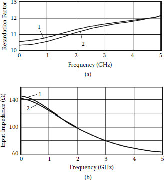
FIGURE 2.15
(a) Retardation factor and (b) input impedance of helical system with plane symmetry versus frequency at x1 = 1, x2 = 2, x31 = 2.5, x32 = 2.5, x41 = 7.5, x42 = 7.5, x5 = 8, x6 = 9, x7 = 10, L = 2, l = 1, p = 0.25, wmn = 1, w41 = 10 mm, εr41 = 5.
Presented results testify that, using modern computers, we can realize calculations of slow-wave system characteristics (retardation factor and input impedance versus frequency), avoiding derivation of analytical expression of the dispersion characteristic. Calculations are fast. Even using a computer with relatively low parameters (300 MHz, 64 MB), they last only a few seconds.
2.8.2 Simulation of an Axially Symmetrical Helical System
Simulation of relatively simple helical systems with axial symmetry using electrodynamical (Section 2.2) and MCL [2] methods revealed some important advantages of these systems.
The cross-section view of the axially symmetrical helical system (Figure 2.16a) is similar to that of the helical system with plane symmetry (Figure 2.11a). At the same time, it is important that elements of the system in Figure 2.16(a) are symmetrical with respect to its central axis, labeled C.
The generalized model of the axially symmetrical helical system developed for simulation and design is presented in Figure 2.16(b). The model consists of axially symmetrical sections of MCLs.
Segments of one-row MCLs with one conductor in a period are used in sections 41*, 42*, 21*, 11,21,41, and 42. Voltages and currents on the conductors in these sections are given by Equations (2.167) and (2.168).
Sections 12, 22*, and 22 contain segments of two-row MCLs with one conductor in a period. Expressions for voltages and currents of conductors in these sections are the same as Equations (2.169) and (2.170).
Finally, the segments of MCLs in sections 3* and 3 contain four rows and one conductor in a period. Voltages and currents on conductors in these sections can be presented by superposition of four TEM waves [2]:
U_31n=(U_1+U_2+U_3+U_4)e−jnθ, |
(2.176) |
I_31n=j(ϒ1E0I_1+ϒ1EπI_2+ϒ1M0I_3+ϒ1MπI_4)e−jnθ, |
(2.177) |
U_32n=(U_1−U_2+U_3−U_4)e−jnθ, |
(2.178) |
I_32n=j(ϒ2M0I_1−ϒ2EπI_2+ϒ2M0I_3−ϒ2MπI_4)e−jnθ; |
(2.179) |
U_33n=(−U_1+U_2+U_3−U_4)e−jnθ, |
(2.180) |
I_33n=j(−ϒ2M0I_1+ϒ2EπI_2+ϒ2M0I_3−ϒ2MπI_4)e−jnθ, |
(2.181) |
U_34n=(−U_1−U_2+U_3+U_4)e−jnθ, |
(2.182) |
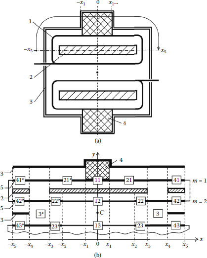
FIGURE 2.16
(a) The cross section of the axially symmetrical helical system and (b) its model. 1: Helix; 2: internal shield; 3: external shield; 4: dielectric holder; 5: conductor of MCL modeling helical conductor of the system.
and
I_34n=j(−ϒ1M0I_1−ϒ1EπI_2+ϒ2M0I_3+ϒ1MπI_4)e−jnθ; |
(2.183) |
where
U_i=A_i1sinkx+A_i2coskxI_i=A_i1coskx−A_i2sinkx
i is an integer (i = 1, 2,3,4)
Υ1E0 = Υ1E(0,θ), Υ1Eπ = Υ1E(π, θ), Υ2E0 = Υ2E(0, θ), Υ2Eπ = Υ2E(π, θ) are characteristic admittances of the MCL containing two rows and obtained using a central electric wall
Υ1M0 = Υ1M(0,θ), Υ1Mπ = Υ2Mπ. Υ2M0 = Υ2M(0, θ), Υ2Mπ = Υ2M(π, θ) are characteristic admittances of the MCL containing two rows and obtained using a central magnetic wall in the model (Figure 2.16)
If an electromagnetic wave in the system is excited using opposite voltages, symmetry conditions must be satisfied:
(2.184) |
(2.185) |
(2.186) |
and
(2.187) |
Substituting expressions for voltages and currents into Equations (2.184),(2.185),(2.186),(2.187), we can eliminate part of the amplitude coefficients, simplify expressions for voltages and currents, and further consider only the upper part of the model.
Upper rows (m = 1; 2) of the MCL model helix if these boundary conditions are satisfied are
We can obtain a mathematical model of the axially symmetrical helical system acting in the same way as in the case of the helical system with plane symmetry. Substituting expressions for voltages and current into Equation (2.188), we obtain a set of homogeneous algebraic equations. In order to find solutions of the dispersion equation, we can compose the matrix containing multipliers at amplitude coefficients of the set of equations. The algorithm presented in Figure 2.13 can be used to search for solutions of the dispersion equation at selected values of phase angle θ. Using Equations (2.172) and (2.174), we find frequency and, corresponding to it, the retardation factor.
The input impedance of the axially symmetrical helical system at x = 0 is given by
where
Υ = Υ42(θ) is the characteristic admittance of the one-row MCL
Υ0 = Υ3(0,θ) is the characteristic impedance of the two-row MCL in the case of the even mode
Υπ = Υ3(π, θ) is the characteristic impedance of the two-row MCL in the case of the odd mode
2h is the length of the helix turn
Calculated characteristics of the vacuumed axially symmetrical helical system (at εr = 1) are presented in Figure 2.17.
According to Figure 2.17(a), the retardation factor of the axially symmetrical system is greater than the retardation factor of the system with plane symmetry. It actually exceeds the value of the structural retardation factor kRs = 2h/L. We can explain this, taking into account that currents in the central rows of the model of the system flow in the same direction. As a result, the coupling of electromagnetic fields is followed by increase of distributed inductance and higher value of the retardation factor. Because of the surface character of the electromagnetic field, the coupling decreases with frequency; as a result of this, the retardation factor decreases with frequency and approaches the value of the structural retardation factor.

FIGURE 2.17
(a) Retardation factor; (b) input impedance of axially symmetrical helical system versus frequency at x1 = 1, x2 = x1, x3 = 4.7, x4 = 4.8, x5 = 5, L = 2, l = 1, p = 0.1 mm, εr = 1. 1: wmn = 0.4, w2n = 0.4 mm; 2: wmn = 0.4, w2n = 2.4 mm.
The input impedance of the axially symmetrical helical system decreases with frequency (Figure 2.17b), as in the majority of helical systems.
The characteristics in Figure 2.17(a) testify that we can reduce dispersion of retardation in an axially symmetrical system, increasing the distance between helical electrodes. Unfortunately, sometimes this method for decreasing of dispersion cannot be used. For example, in traveling-wave cathode ray tubes, increased distance between deflecting electrodes is followed by decreased sensitivity of the tube.
On the other hand, taking into account general properties of helical systems [2], we can use the other method for improving dispersion properties of axially symmetrical helical systems. Due to dielectric holders of helices, we can increase retardation in the high-frequency range. Thus, using dielectric holders, we can compensate for the inherency for axially symmetrical helical systems’ decreasing of the retardation factor with frequency. The characteristic presented in Figure 2.18(a) confirms the correctness of this idea. Unfortunately, dielectric holders cause additional increase of distributed capacitances of helical electrodes with frequency. This is followed by additional decrease of input impedance with frequency. The frequency characteristic of input impedance for an axially symmetrical helical system containing dielectric holders is presented in Figure 2.18(b).
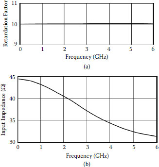
FIGURE 2.18
(a) Retardation factor and (b) input impedance of the axially symmetrical helical system versus frequency at x1 = 0.25, x2 = 3.3, x3 = 3.3, x4 = 4.45, x5 = 4.7, L = 2, l = 0.5, p = 0.25, wmn = 0.4, w11 = 3 mm, εr11 = 7.
Thus, we can find frequency characteristics of complex slow-wave systems, avoiding derivation of the dispersion equation and using numerical methods for solution of the set of algebraic equations modeling the slow-wave system. This allows saving work and time resources at simulation and design of slow-wave systems. At the same time, using modern software (e.g., software system MATLAB), we can ensure high precision of fast calculations.
2.9 Application of Scattering Transmission Line Matrices
Real slow-wave systems have limited length. The matrix methods developed for four-pole and multipole electric circuits can be used for simulation of slow-wave systems with limited length. In this section, we will consider application of the scattering transmission line matrices for analysis of frequency properties of wide-band slow-wave systems. We will reveal the relationship between the matrix of S parameters and elements of the A B C D matrix. Later, we will illustrate the composition and application of the scattering transmission line matrix in an example of the meander slow-wave system. Results obtained using scattering transmission line matrices will be compared with known results of simulation and experimental investigation.
This section is based on results published in references 20–25.
2.9.1 Two-Port Circuits in Models of Periodic Systems
Models containing four-pole (two-port) circuits can be used for analysis and calculations of frequency characteristics of slow-wave systems with limited length. The general model of a system is presented in Figure 2.19(a). The matrix of ABCDsws parameters (Figure 2.19b) can be used to characterize the slow-wave system. Then, the relationship between the input and output voltages and currents is given by a matrix equation of the form:
(U_1I_1)=(A_swsB_swsC_swsD_sws)(U_2I_2), |
(2.190) |
where U1 and I1 are complex amplitudes of input voltage and input current flowing into the four-pole circuit, and U2 and I2 are complex amplitudes of output voltage and output current flowing from the four-pole circuit.

FIGURE 2.19
(a) The model of the signal path in a slow-wave device and two-port circuits with (b) A B C D and (c) S parameters modeling the device.
In the case of a homogeneous electromagnetic line, elements of the ABCDsws matrix are dependent on the propagation constant and the length of the line [23]
A_sws=cos(γlsws),B_sws=Zcsinh(γlsws),C_sws=1Z_csinh(γlsws)D_sws=cosh(γlsws), |
(2.191) |
where
γ = α + jβ is propagation constant
α is attenuation coefficient
β is phase constant
Zc is characteristic impedance of the system
lsws is system length
At known (ABCD)sws parameters, we can find input impedance ZIN, characteristic impedance Zc, and transfer function K of the system:
Z_IN=A_swsZ_L+B_swsC_swsZ_L+D_sws,zc=√B_swsC_sws, |
(2.192) |
K_=U_2E_s=Z_LZ_IN.Z_IN+Z_iA_swsZ_L+B_sws+C_swsZ_iZ_L+D_swsZ_i, |
(2.193) |
where Es is electromotive force of the signal source, Zi is its internal impedance, and ZL is the load impedance.
The system of A B C D parameters was developed for lumped-constant circuits. The scattering S parameters are preferable for circuits with distributed parameters, transmission lines, and slow-wave systems (Figure 2.19c).
With application of S parameters, input and output voltages and currents can be described using complex scattering components ai and bi characterizing incident and reflected waves from ports of the circuit:
U_i=U_Ii+U_Ri=√Z_ci(a_i+b_i), |
(2.194) |
I_i=1Z_ci(U_li−U_Ri)=1√Z_ci(a_i+b_i), |
(2.195) |
where
Ui, Ii are complex amplitudes of voltage and current at the ith port
Uli, URi are complex amplitudes of the incident to the ith port and reflected from the it ith port waves
ai, bi are complex amplitudes of the incident and reflected scattering components
According to Equations (2.194) and (2.195), the scattering parameters are related to the voltages Uli, URi and currents IIi, IRi and can be determined using the following equations:
a_i=U_Ii√Z_Ci=I_Ii√Z_Ci=12(U_i√Z_Ci+I_i√Z_Ci), |
(2.196) |
b_i=U_Ri√Z_Ci=I_Ri√Z_Ci=12(U_i√Z_Ci+I_i√Z_Ci). |
(2.197) |
The reflected scattering parameters b1, b2 and the incident scattering parameters a1, a2 are related by
(2.198) |
(2.199) |
where S_sws11,S_sws12,S_sws21,S_sws22 are scattering or Ssws parameters of the system.
At known Ssws parameters, we can find (ABCD)sws parameters using Equation (2.23):
(2.200) |
(2.201) |
(2.202) |
and
(2.203) |
Thus, using scattering parameters, we can take into account processes in electrodynamical systems and slow-wave structures and find the main frequency characteristics of the devices.
2.9.2 Composition of Scattering Matrix for Multiconductor Lines
Let us assume that the MCL modeling a slow-wave system consists of N conductors. Because a conductor has input and output, the 2N-port circuit can be used for modeling of the MCL and the system. Figure 2.20 illustrates the MCL and the 2N-port circuit corresponding to it.
Scattering parameters of the 2N-port circuit are related by
b_1=S_11a_1+S_12a_2+…+S_12Na_2N,b_2=S_21a_1+S_22a_2+…+S_22Na_2N,⋮⋮⋮…⋮b_2N=S_2N1a_1+S_2N2a_2+…+S_2N2Na_2N. |
(2.204) |
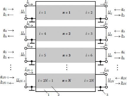
FIGURE 2.20
2N-port circuit superposed with topology of the MCL. 1: 2N-port circuit; 2: conductor of the MCL; 3: shield of the MCL; n: the order number of the MCL; i: the number of the port; U, Ii: complex amplitudes of voltage and current at the ith port; ai, bi; complex amplitudes of incident and reflected components at the ith port.
The set in Equation (2.204) can be represented in matrix form:
(b_1b_2⋮⋮b_2N)=(S_11S_12……S_12NS_21S_22……S_22N⋮⋮⋮⋮⋮⋮⋮⋮⋮⋮S_2N1S_2N2……S_2N2N)(a_1a_2⋮⋮a_2N) |
(2.205) |
or
(2.206) |
The S matrix is the scattering matrix of the MCL. It contains 2N × 2N elements. Elements Sij correspond to reflections from the ith port; elements Sij characterize transfer from the jth to the ith port.
Let us compose the scattering matrix for the MCL containing identical conductors (d1 = d2 = d) and identical gaps (l1 = l2 = l) among them. Then the MCL is the periodic structure and, using electric and magnetic walls, we can divide it into N two-port circuits. As is known, magnetic walls can be used at the same voltages of conductors (un = u) and propagation of the even mode (Figure 2.21a). Electrical walls can be used at the opposite voltages of neighboring conductors (un = −un±1) and propagation of the odd wave (Figure 2.21b).

FIGURE 2.21
Magnetic and electric walls in the cross section of the multiconductor line at (a) odd and (b) even modes in the line. 1: Conductor of the line; 2 and 4: shields; 3: dielectric substrate; n: order number of the conductor of the line.
The ABCD parameters of a transmission line in Figure 2.21 are dependent on characteristic impedance, wave number, and length of the line 2h. At propagation of even and odd waves without attenuation, expressions of the ABCD parameters are given by
A_e,o=cos(ke,o2h),B_e,o=j1ϒe,osin(ke,o2h),C_e,o=jϒe,osin(ke,o2h),D_e,o=cos(ke,o2h). |
(2.207) |
Characteristic admittances and wave numbers for even and odd waves (Υe, ke, and Υo, ko) can be found using Equations (2.88),89,90,91,92,(2.93), (2.96), and (2.97).
At known elements of matrices (ABCD)e and (ABCD)o for even and odd waves, elements of corresponding scattering matrices Se and So can be found using the following expressions [24]:
(2.208) |
(2.209) |
(2.210) |
and
(2.211) |
At known scattering parameters S11e,o, S12e,o, S12e,o, and S22e,o we can compose the scattering matrix S for the MCL. At electric and magnetic walls, we take into account only coupling of neighboring conductors of the MCL. As a result, the S matrix is a sparse matrix:
s_=(s_1s_1200…0s_21s_2s_230…0⋮…⋮⋮…⋮0…s_n(n−1)s_ns_n(n+1)0⋮…⋮⋮…⋮0…00s_N(N−1)s_N). |
(2.212) |
Thus, according to Equation (2.212), the s_ matrix is a square matrix containing N x N elements. It can be considered as consisting of square (2 × 2) sn_ ,sn(n±1) and 0. The matrices sn_ are in the positions along the main diagonal of the matrix S. The matrix Sn contains S parameters of the nth conductor of the MCL:
(2.213) |
where
(2.214) |
(2.215) |
Matrices s_n(n±1) take positions in the matrix S along neighboring diagonals with respect to the main diagonal. Elements of matrices Sn (n±1) characterize the influence of the neighboring conductors on the nth conductor. They are given by
(2.216) |
(2.217) |
Figure 2.22 illustrates the mentioned influence and the nature of elements of matrices s_n(n−1). Figure 2.22(a, b) helps to find the structure of the matrix s_n(n+1), and Figure 2.22(c, d) allows determination of elements of the matrix s_n(n+1). Thus, the elements of the matrices s_n(n+1) are given by
(2.218) |
(2.219) |
(2.220) |
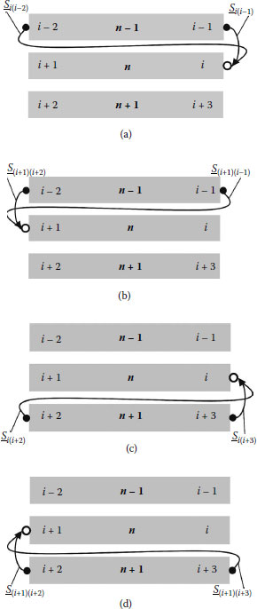
FIGURE 2.22
The influence of neighboring conductors on the nth conductor and corresponding S parameters evaluating the influence.
and
(2.221) |
The symbol 0 in Equation (2.212) denotes the square (2 x 2) matrix with zero elements.
As an example, the S matrix for an MCL consisting of three conductors (N = 3) is the following:
s_=(s_111s_112s_13s_1400s_121s_122s_23s_2400s_131s_132s_211s_212s_35s_36s_141s_142s_221s_222s_45s_4600s_53s_54s_311s_31200s_63s_64s_321s_322). |
(2.222) |
Thus, the matrix contains 6 × 6 elements. Scattering parameters S_1ij=S_2ij and S_3ij characterize the first, second, and third conductors, respectively. Scattering parameters S13, S14, S23, and S24 characterize the influence of the second conductor on the first conductor; parameters S31, S32, S41, and S42 characterize the influence of the first conductor on the second conductor. The last scattering parameters define the influence of the third conductor on the second conductor and the influence of the second conductor on the third conductor.
2.9.3 Meander Slow-Wave System Model Based on Scattering Parameters
Let us demonstrate application of the scattering matrix method for simulation of the planar meander slow-wave system presented in Figure 2.23. The system consists of the dielectric substrate with the meander electrode on it. The bottom side of the substrate is metalized and acts as a shield.
We use several steps to form the model of the meander slow-wave system:
1. We select the MCL corresponding to the meander system and compose its S matrix. The structure and dimensions of the MCL must be the same as in the meander line. To compose the S matrix, we find characteristic impedances of conductors of the MCL and wave numbers for the even and odd modes (Υe, ke and Υo, ko). Later, we compose (ABCD)e and (ABCD)o matrices for conductors and transform them to S parameters (Se and So corresponding to the even and odd waves). At known S parameters, we find scattering parameters Stj and form the S matrix of the MCL.
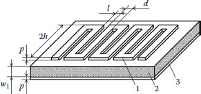
FIGURE 2.23
Meander slow-wave system. 1: Meander electrode; 2: dielectric; 3: shield.
2. We write the matrix equation describing the MCL with matched voltage sources U1 and U2 at the input and output ports, taking into account that scattering parameters of the sources are zero [23]:
(2.223) |
or in the matrix form of
(2.224) |
where b′, a′, and S′ are scattering matrices of scattering components and scattering parameters of the MCL and voltage sources; b, a, and S are matrices of scattering components and S parameters of the MCL.
(2.225) |
are matrices describing scattered parameters bUi, aUi, and SUi of the voltage sources and U is the matrix of voltages Ui. At matched voltage sources, scattering from the sources is zero, so Su1 = Su2 = 0. Then the matrix S′ is obtained, adding two rows and two columns with zero elements to the matrix S.
3. We transform the matrix equation describing the MCL to the form corresponding to the meander electrode. At the same scattering components at the junctions of the internal ports, the S′ matrix is the model of the meander system.
Figure 2.24 illustrates the last idea. At the junction of the jth and the kth port,
(2.226) |
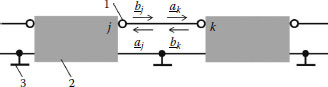
FIGURE 2.24
The junction of the jth and the kth ports in the 2N-port circuit modeling the MCL. 1: The pole of the internal port; 2: conductor of the MCL; 3: shield.
or, in matrix form,
(2.227) |
Then, the matrix describing all junctions in the model of the MCL can be presented in the form of
(2.228) |
where Γ is the matrix describing all internal connections in the model of the meander electrode (including connections of the voltage sources).
The Γ matrix is the sparse matrix. Only elements corresponding to the intersections of rows and columns corresponding to the numbers of the connected ports are different from zero. For example, at the junction of the jth and the kth ports, elements Γjk and Γkj are equal to 1. The last elements are zero.
After substitution of Equation (2.228) into Equation (2.224), we obtain
(2.229) |
Then,
(2.230) |
where
(2.231) |
is the matrix describing connections. Elements along the diagonal of this matrix are multiplied by -1 reflection coefficients from the ports. Elements with indices ij are equal to multiplied by -1 values of the transfer coefficients between corresponding ports. The elements that do not correspond to connected ports are zero. Thus, elements of the matrix depend only on connections and structure of the slow-wave structure and do not depend on parameters of conductor or frequency.
4. We find scattering parameters S_SWS11=S_SWS12 , S_SWS21, and S_SWS22. At known scattering matrix a′, using Equation (2.228), we can find the matrix b′, that is the scattering matrix describing internal and external ports. At known b′, we can find scattering parameters of the meander system:
(2.232) |
(2.233) |
5. At known scattering parameters, using Equations (2.200),(2.201),(2.202),(2.203),(2.204), we find the (ABCD)sws matrix. Finally, using Equations (2.192) and (2.193), we can find frequency characteristics: input impedance ZIN(f), characteristic impedance Zc(f), and transfer function K(f).
In Equation (2.232), b1 denotes the scattering component reflected from the input at matched load impedance of the meander system; b2N has meaning of the output scattering component at matched voltage source (U1 = 1) at the input. In Equation (2.233), b1 denotes the scattering component reflected from the output at matched load at the input; finally, b2N is the input scattering component at matched voltage source (U1 = 1) at the output.
Let us illustrate application of the described method for the meander system consisting of three conductors. The circuit modeling the system consisting of three two-port circuits and voltage sources is presented in Figure 2.25.
The scattering matrix S of the multiconductor line consisting of three conductors is given by Equation (2.222). According to Figure 2.25, the matrix of connections is of the form
Γ=(0000001000100000010000000000100000010000000000011000000000000100). |
(2.234) |
Thus, in Equation (2.234), only elements corresponding to the connected poles (Figure 2.25) are not zero.

FIGURE 2.25
The model of the meander system consisting of three conductors.
Using Equation (2.230), we can compose the scattering matrix W. To this end, taking into account the voltage sources, we add two rows and two columns with zero elements to the matrix S and form the S’ matrix containing 8 × 8 elements:
s_ ′=(s_111s_112s_13s_140000s_121s_122s_23s_240000s_31s_32s_211s_212s_35s_3600s_41s_42s_221s_222s_45s_460000s_53s_54s_311s_3120000s_63s_64s_321s_322000000000000000000). |
(2.235) |
Then, substituting Equations (2.234) and (2.235) into Equation (2.230), we obtain the scattering matrix W describing connections:
The matrix U describing matched voltage sources contains eight rows and one column. The first six elements in the column are zero. The last elements are U1 and U2.
Thus, the solution of the matrix Equation (2.229) is of the following form:
(2.237) |
At known matrix a’, using Equation (2.228), we can find the W’ matrix. Then, we can find the scattering parameters of the meander system using Equations (2.232) and (2.233). U1 = 1 and U2 = 0, the scattering components b1 and U6 give scattering parameters S_SWS11 and S_SWS21. At U1 = 0 and U2 = 1, scattering components b1 and b2 give S_SWS12 and S_SWS22.
We verified suitability of the scattering matrix method for simulation of meander slow-wave systems, comparing computational and experimental results obtained for the microstrip meander line (Figure 2.23) at the number of conductors in the line N = 55, width of a conductor d = 0.64 mm, its length 2h = 55 mm, thicknesses of the meander electrode and the shield p = 0.01 mm, gaps among the conductors l = 0.35 mm, thickness of the substrate w1 = 0.5 mm, and relative dielectric permittivity of the substrate εr1 = 9.85.
We applied the scattering matrix and the multiconductor line methods for simulation of the line and calculation of its phase delay time and characteristic impedance. In the application of the scattering matrix method, we imitated a technique developed for experimental investigation [1,2] and based on the input impedance frequency characteristic ZIN(f) for the short-circuited end of the line.
As an example, the calculated characteristic ZIN(f) is presented in Figure 2.26. The phase delay time can be found at resonant frequencies of the line. The frequency characteristic of the phase delay time, found using the described method, is presented by curve 1 in Figure 2.27. Curve 2 is plotted using the multiconductor line method, and curve 3 represents experimental results.

FIGURE 2.26
Modulus of input impedance of meander line versus frequency.

FIGURE 2.27
Delay time of the meander delay line versus frequency. 1: Using the scattering matrix method; 2: using the multiconductor line method; 3: according to measurement.
The dispersion of results presented in Figure 2.27 is less than 5%. In the low-frequency range, results obtained using the scattering matrix method practically coincide with experimental results.
The deviation of values of characteristic impedance in the low-frequency range obtained using the scattering matrix and the multiconductor line methods from experimental results was less than 2%. Thus, the scattering matrix method can be applied for simulation of slow-wave systems. We applied this method for investigation of meander slow-wave systems with limited length. (Results are presented in Chapter 7.)
We considered propagation of electromagnetic waves in the generalized multiconductor line intended for modeling of periodic slow-wave structures.
The plane complex transverse (TEM or T) electromagnetic wave can propagate along the multiconductor line containing N conductors in the period at homogeneous or nonhomogeneous dielectric in the cross section of the line. The wave consists of an infinite number of space harmonics (i.e., harmonic waves with the same frequency ω and different phase velocities vph). The space harmonics propagate together. The periodic boundary conditions for a separate space harmonic are not satisfied.
The complex amplitudes of voltages and currents on the conductors of the multiconductor line containing N conductors in the period can be presented in the form of the sum of N components that are called normal waves, which are TEM waves. With a homogeneous dielectric, phase velocities of normal waves are the same. With a nonhomogeneous dielectric, distribution of the electric field in the cross section of the multiconductor line changes with frequency. As a result, the effective dielectric permittivities, the phase constants characterizing propagation of normal waves along the line, and phase velocities of the normal waves are dependent on frequency. Some parameters are necessary to characterize processes in the multiconductor line at frequency ω: characteristic admittances of conductors Υn(θv) and values of relative dielectric permittivity εr ef(θv) for normal waves (dependent on phase angles θv between voltages or currents on neighboring conductors of the line).
We examined voltages and currents in the multiconductor lines that contain two different conductors in the period and can be used for modeling of the wide-band slow-wave systems with zero critical frequency. Two types of normal waves (modes) can propagate in this instance. They can be excited at particular relationships between magnitudes and phases of voltages and currents at the input of lines. The terms slow and fast characterize phase velocities of the modes. The terms c-mode and π-mode are related to excitation of the modes: At c-mode, polarities of voltages of neighbor conductors are the same, but at π-mode they are opposite; in the case of asymmetrical coupled lines, magnitudes of voltages are different.
With identical conductors, one type of normal wave can be excited at the same amplitudes and the same phases of voltages. This type of normal wave is called the even mode. For the other type of normal wave, amplitudes of voltages must be the same, but phases must be opposite. This type of normal wave is called the odd mode.
In order to reveal properties of normal waves, values of inherent capacitances C11, C22 and mutual capacitances C12 = C21 per unit of length are necessary. Taking into account these parameters, expressions for calculation of ratio Rc and Rπ of complex amplitudes of voltages on neighboring conductors at c-mode and π-mode, as well as effective dielectric permittivities εr ef c, εr ef π and characteristic admittances Υ1c, Υ1π, Υ2c, and Υ2π, are derived.
At ratio of voltages different from Rc or Rπ the wave process in the multiconductor line can be considered as a result of superposition of normal waves. Expressions for calculation of inherent capacitances C1(θ), C2(θ), characteristic admittances Υ1(θ), Υ2(θ), and effective dielectric permittivity εr ef(θ) are derived. At superposition, the mentioned parameters change periodically with phase angle θ, and the period is 2π.
Magnetic and electric walls can be used in models of the multiconductor lines at propagation of even and odd waves. In these instances, we recommend using conceptions or partial capacitances to simplify calculations of inherent and mutual capacitances.
We propose the technique for analysis of the wide-band slow-wave systems using the multiconductor line method. At a selected multiconductor line corresponding to the slow-wave system, known characteristic admittances Υ(θv), and effective dielectric permittivity εr ef(θv), taking into account boundary conditions, we can derive the set of algebraic equations that is a mathematical model of the system. Solving the set of equations, we can derive the dispersion equation of the system and, later, find its retardation factor and input impedance.
In the case of nonhomogeneous systems, models containing some segments of multiconductor lines are used. Then it is not easy to derive the analytical expression of the dispersion equation. A method based on application of matrix algebra has been developed for modeling and simulation of complex systems. Properties of the complex meander system with axial symmetry can be discovered using this method.
In the analysis of complex nonhomogeneous systems, derivation of the dispersion equation is complicated, even though the methods of matrix algebra are used. We can avoid the tedious work necessary for derivation of the analytical expression of the dispersion equation by using numerical methods for solution of the set of equations describing the model of the system. Application of this method is illustrated in the example of a complex helical system with axial symmetry.
Real slow-wave systems have limited length. Matrix methods developed for two-port and multiport electric circuits can be used for simulation of slow-wave systems with limited length. A method based on scattering transmission line matrices has been developed for analysis of frequency properties of wide-band slow-wave systems with limited length.
1. Vainoris, Z., Kirvaitis, R., and Staras, S. 1986. Electrodynamic delay and deflection systems. Vilnius, Lithuania: Mokslas, 266. [In Russian.]
2. Staras, S. et al. 1993. Super-wide band tracts of the traveling-wave cathode-ray tubes. Vilnius, Lithuania: Technika, 360. [In Russian.]
3. Martavicius, R. 1996. Electrodynamic plain retard systems for wide-band electronic devices. Vilnius, Lithuania: Technika, 264. [In Lithuanian.]
4. Burokas, T. 2006. Modeling and simulation of the super-wide-band slow-wave and deflection structures. Doctoral dissertation, Vilnius, Lithuania, Vilnius Gediminas Technical University, 179. [In Lithuanian.]
5. Jurjevas, A. 2001. Investigation and CAD of meander systems. Doctoral dissertation, Vilnius, Lithuania, Vilnius Gediminas Technical University, 145. [In Lithuanian.]
6. Vainoris, Z. 2004. Fundamentals of wave electronics. Vilnius, Lithuania: Technika, 513. [In Lithuanian.]
7. Silin, R. A., and Sazonov, V. P. 1968. Slow-wave systems. Moscow: Sov. Radio, 632. [In Russian.]
8. Floquet, G. 1883. Sur les equations differentielles lineaires a coefficients periodique. Annales Scientifiques de l’École Normale Supérieure 2 (12): 47–89.
9. Altshuler, J. G., and Trohimenko, J. K. 1963. Low power backward-wave tubes. Moscow: Sov. Radio, 296. [In Russian.]
10. Krage, M. K., and Haddad, G. I. 1970. Characteristics of coupled microstrip transmission lines—I: Coupled-mode formulation of inhomogeneous lines. IEEE Transactions on Microwave Theory and Techniques 18 (4): 217–222.
11. Hayden, L. A., and Tripathi, V. K. 1994. Characterization and modeling of multiple line interconnections from time domain measurements. IEEE Transactions on Microwave Theory and Techniques 42(9): 1737–1743.
12. Schmiedel, H. 2004. Series-configuration of multi-line directional-coupler sections with improved coupling. Microwave Symposium Digest, IEEE MTT-S International, June 6–11, 1:339–342.
13. Skudutis, J., and Staras, S. 1996. Modeling of super-wide-band slow-wave structures. Proceedings of the 5th Biennial Baltic Electronics Conference. Tallinn, Estonia, 1996, October 7–11, 457–460.
14. Staras, S., and Skudutis, J. 1996. The influence of dielectric holders on characteristics of the meander slow-wave structures. Baltic Electronics 2 (1): 37–38.
15. Itoh, T., Pelosi, G., and Silvester, P. S. 1996. Finite element software for microwave engineering. New York: John Wiley & Sons, 478.
16. Taflove, A. 1998. Advances in computational electrodynamics: The finite-difference time-domain method. London: Artech House, 728.
17. Pelosi, G., Coccioli, R., and Selleri, S. 1998. Quick finite elements for electromagnetic waves. London: Artech House Books, 265.
18. Kleiza, A., and Staras, S. 2000. Analysis of complicated retard systems without derivation of dispersion equation. Electronics and Electrical Engineering 6 (29): 65–71. [In Lithuanian.]
19. Burokas, T., Daskevicius, V., Skudutis, J., and Staras, S. 2005. Simulation of the wide-band slow-wave structures using numerical methods. EUROCON 2005, Computer as a Tool. Belgrade, I:848–851.
20. Tascone, R., Savi, P., Trinchero, D., and Orta, D. 2000. Scattering matrix approach for the design of microwave filters. IEEE Transactions on Microwave Theory and Techniques 48 (3): 423–430.
21. De Padua Moreira, R., and De Menezes, L. R. 2000. Direct synthesis of microwave filters using inverse scattering transmission-line matrix method. IEEE Transactions on Microwave Theory and Techniques 48 (12): 2271–2276.
22. Hsin-Chia, L., and Tah-Hsiung, C. 2000. Port reduction methods for scattering matrix measurement of an N-port network. IEEE Transactions on Microwave Theory and Techniques 48 (6): 959–968.
23. Gupta, K.C., Garg, R., and Chadha, R. 1987. Computer-aided design of microwave circuits. Moscow: Radio i sviazj, 432. [In Russian.]
24. Gurskas, A., Jurevicius, V., Kirvaitis, R., and Sileikis, A. 2002. Application of scattering matrices in investigation of electrodynamic systems, Electronics and Electrical Engineering 4 (39): 7–12. [In Lithuanian.]
25. Gurskas, A., Kirvaitis, R., Martavicius, R., and Sileikis, A. 2002. Simulation of electromagnetic field in microstrip meander lines by three-dimensional tangential finite-element method and scattering matrices method. Electronics and Electrical Engineering 6 (41): 30–35. [In Lithuanian.]