
Application of Slow-Wave Structures for Deflection of Electron Beams
Electronic oscilloscopes are widely applied for display of form and measurement of parameters of electric signals. Traveling-wave oscilloscopes with traveling-wave cathode-ray tubes have been developed for investigation of single short electric pulses and fast nonrepetitive processes. The idea of the traveling-wave cathode-ray tube (TW CRT) and the traveling-wave deflecting system was proposed by A. V. Haeff [1].
In a traveling-wave deflecting system, the signal wave propagates along the electrodynamical deflecting system. The velocity of the wave must be close to the velocity of the electrons of the electronic beam. Because the velocity of the electrons in the beam is less than the velocity of light, slow-wave structures are necessary for TW CRTs. The frequency spectrum of short pulses and fast processes is wide, so deflecting systems with super-wide pass-bands (from 0 to some gigahertz) are necessary.
The width of the pass-band of TW CRT is mostly dependent on variation of the retardation factor and characteristic impedance of the traveling-wave deflecting system [2,3,4,5]. For this reason, dispersion of retardation and change of characteristic impedance must be minimal in traveling-wave deflecting systems.
The important results of research in the field of TW CRTs and their deflecting systems are presented in references 4,5,6,7. There, models for analysis of processes in traveling-wave deflecting systems and cathode-ray tubes are developed, calculation and experimental methods for determination of parameters and characteristics of the tubes and deflecting systems are proposed, the influence of various factors on frequency and transient responses are discovered, and design methods and new technical solutions for traveling-wave deflecting systems are proposed.
On the other hand, new challenges have appeared in the field of TW CRTs and traveling-wave deflecting systems. The new results achieved by researchers after publishing [5] are presented in this chapter.
In Staras and Skudutis [8], possibilities of frequency distortion reduction based on compensation methods are considered. On the basis of Staras and Kleiza [9] and Staras and Burokas [10], analysis of the structure of a deflecting electromagnetic field and the results of calculation and analysis of the transverse component of zero spatial harmonics of an electric field are presented. Nonlinear distortions [11,12] of signals in TW CRTs are considered.
A simplified model of the signal path in TW CRTs for analysis of processes in transitions to traveling-wave deflecting systems is proposed, and the influence of transitions on properties of traveling-wave deflecting systems and TW CRTs is discovered [13,14,15]. Finally, possibilities of improvement of traveling-wave deflecting systems and TW CRTs are revealed and considered [16].
7.1 Correction of Phase Distortions in Traveling-Wave Deflecting Systems
The width of the pass-band and operation speed of TW CRTs and traveling-wave oscilloscopes depend on many factors [4,5,6,7]. Usually, the main factor is dispersion of the phase velocity (and delay time) of the electromagnetic wave in the traveling-wave deflecting system. It is impossible to ensure the necessary width of the pass-band AF and less than 10% variation of the flat part of the transient response if Δtd × ΔF > 0.05, where Δtd is the phase delay time dispersion in the given pass-band [5].
The velocity of electrons in the electron beam depends on accelerating voltage. If dispersion of an electromagnetic wave exists, the velocities of electrons and wave can be matched only in the limited frequency range. Additionally, phase-frequency distortions of the signal in the traveling-wave deflecting system and distortions of the signal form on the tube screen arise.
According to references 4–7 and data presented in previous chapters, various methods have been developed to reduce dispersion. On the other hand, the dispersion allowed in super-wide-band deflecting systems is very small. Even deflecting systems for tubes with ΔF ≥ 5 GHz are complicated and must be precisely manufactured.
The principles of phase correction are widely used in electronic circuits in order to reduce phase-frequency distortions. Taking this into account, it is important to consider possibilities of phase correction in traveling-wave oscilloscopes. In this instance, processes are more complicated. At the input of the deflecting system, an undistorted signal acts on the electron beam. Distortions of the deflecting signal increase at its propagation along the deflecting system. At the same time, it is important that the influence of the signal (and its distortions) on the beam decreases with its approach to the end of the system.
The signal path of the traveling-wave oscilloscope containing a phase corrector is presented in Figure 7.1. The transfer function of the signal path is given by
(7.1) |
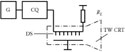
FIGURE 7.1
Signal path. G: Signal source (generator); CQ: corrective quadripole; DS: deflecting system; RL: load resistance.
where
KT(jω) is the transfer function of the TW CRT
KC(jω) is the transfer function of the phase corrector (corrective quadripole)
KG(jω) is the transfer function of signal source (generator)
Using transfer function KG(jω), we can simulate a voltage step with the rise time tg or frequency distortions in the TW CRT caused by other factors [4,5].
The transfer function of the tube is given by [8]
(7.2) |
where
(7.3) |
(7.4) |
The transfer function of the phase corrector can be approximated by
(7.5) |
where k is the correction coefficient.
Taking k = 1, we can simulate the signal path without the corrector. At k = 1, the change of the phase in the corrector is opposite to the change of the phase in the deflecting system (phase-frequency distortions are compensated at the end of the deflecting system).
We can approximate the transfer function KG(jω) using the following formulas:
(7.6) |
(7.7) |
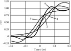
FIGURE 7.2
Transient responses of a TW CRT at various values of correction coefficient k. 1: k = 0; 2: k = 0.5; 3: k = 1; 4: k = 0.5 and optimal accelerating voltage.
and
(7.8) |
where x = ωζ/2, ζ = 1.25tg; z = O.lx.
The transient responses corresponding to the transfer function (Equation 7.1) at various values of correction coefficient k are presented in Figure 7.2. Calculations were made at tg = 0.01 ns, tph = t0 + af, t0 = 2 ns, and a = 0.05 ns/GHz. Curves 1–3 correspond to te = 2.05 ns; curve 4 corresponds to the optimal accelerating voltage (optimal velocity of electrons and optimal transit time).
According to Figure 7.2, it is possible to reduce the influence of wave velocity dispersion using a corrective quadripole at the input of the deflecting system. At te = 2.05 ns, the rise time of the transient response is minimal when k = 0.5 (Figure 7.2, curve 2). Usage of a corrective quadripole with k = 1 is not effective. We can explain this by taking into account that, at k = 1, the phase-frequency characteristic of the circuit consisting of the quadripole and deflecting system becomes linear at the end of the deflecting system. Then the distorted signal acts on the electron beam along the entire system. At k = 0.5, phase distortions of the deflecting signal are minimal at the middle of the system, and the part of the system where a minimally distorted signal causes deflection of the beam is longer.
The graph presented in Figure 7.3(a) confirms the last idea. The rise time of the transient response is minimal at k = 0.5.
Figure 7.3(b) illustrates how the rise time of the transient response depends on transit time te at the optimal value of the correction coefficient (k=0.5). According to the figure, with the application of the optimal corrective quadripole, the transient response can be improved, correcting accelerating voltage. The rise time of the transient response is minimal when wave and electron velocities are matched at higher frequency. In the case when wave velocity increases with frequency, the optimal transit time is greater (the optimal accelerating voltage is less). The transient response with an optimal correction coefficient and optimal accelerating voltage is presented by curve 4 in Figure 7.2.

FIGURE 7.3
The rise time of the transient response versus (a) correction coefficient k and (b) transit time te.
It is impossible to avoid attenuation in a real corrective quadripole. For this reason, the internal correction of phase distortions is a better technical solution. The internal correction can be realized in the deflecting system consisting of two parts. If the phase velocity of the wave in the initial part increases with frequency, the phase velocity in the last part must decrease with frequency, and vice versa. The model of the deflecting system consisting of some parts and software described in Staras et al. [5] was used to check the internal compensation idea.
According to results of calculations [8], using internal compensation, we can reduce the rise time of the transient response and distortions of signals in the deflecting system and TW CRT. Figure 7.4 illustrates how the rise times of transient responses of a TW CRT and its deflecting system depend on the ratio l1/l2 at a constant gap between deflecting electrodes (here, l1 and l2 are the lengths of the parts of the deflecting system).
According to Figure 7.4, the conditions for the best characteristics of the deflecting system (signal path) and TW CRT are different. The rise time of the deflecting system transient response is minimal at l1 = l2. The rise time of the TW CRT is minimal at l1/l2 ≅ 0.5. More detailed information about the internal compensation possibilities is presented in Staras and Skudutis [8].

FIGURE 7.4
The rise time of the transient responses of (a) signal path and (b) traveling wave tube versus ratio of lengths of deflecting system parts.
Thus, according to analysis, methods of phase distortion compensation can be used in the design of TW CRTs and signal paths of traveling-wave oscilloscopes. At the same time it is important that conditions for minimal phase-frequency distortions in traveling-wave cathode-ray tubes and their deflecting systems are different.
7.2 Electrical Field in the Deflecting System
In TW CRTs the electron beam is deflected by a zero spatial component of the transverse electric field. The electromagnetic field in slow-wave structures has surface character [17,18]. For this reason, the strength of the deflecting electrical field decreases with frequency. Such variation of the field causes amplitude-frequency distortions and limits the width of the TW CRT pass-band [4,5,6,7].
Let us consider methods developed for calculation of deflecting field strength and apply the numerical finite difference method for more precise calculations.
7.2.1 Analytical Methods and Approximations
Let us consider a nondispersive helical deflecting system with elongated rectangular cross section. Electrodynamical and multiconductor line methods can be used for analysis of the system.
In the case of the electrodynamical method, an anisotropical plane is used for modeling of the helix. Then the transverse component of the deflecting electric field is given by [4,5]
(7.9) |
where
Um is amplitude of the harmonic deflecting voltage
kph = ω/vph is the wave number
ω is angular frequency
vph is phase velocity of the incident wave propagating along the system
w is the gap between the deflecting electrodes
y is the transverse coordinate (perpendicular to the plane modeling helix)
Using the anisotropic plane in the model of the helical system, we cannot take into account the periodical structure of the system. Assuming that the transit time of the period by an electron is τ and representing the periodical helical deflecting system as a system of periodical deflecting plates, we can evaluate the influence of the transit time on frequency properties of the tube using a coefficient [4,5],
(7.10) |
where θ = ωτ is the phase angle corresponding to the transit time τ.
Then, according to Equations ((7.9)) and ((7.10)),
(7.11) |
On the other hand, the approximation (Equation (7.11)) does not take into account that gaps exist between neighboring helical wires. In practice, the width of the helical conductor can be up to two times less than the period. Then the equivalent width of the conductor can be used to estimate the spread of the field in the real system. Unfortunately, methods for calculation of the equivalent width have not been developed.
Using the multiconductor line method, we can take into account the periodicity of helical structure, the dimensions of conductors, and the gaps among them.
The electrical field of the incident wave (propagating in the z direction) in a periodical structure (Figure 7.5) is given by
(7.12) |
where x and y are transverse coordinates, z is a longitudinal coordinate corresponding to the wave propagation direction, and β is the phase constant.
According to the Floquet theorem, the electric field at a section z + L of a periodic structure is given by
(7.13) |

FIGURE 7.5
The cross section of a shielded multiconductor line. 1: Conductor of the line; 2 and 3: shields.
where determines the field at section z, and product βL describes the delay of the field in the period.
Taking into account the periodicity of the field in the z direction, we can rearrange Equation ((7.12)):
(7.14) |
Here, F(z) is the periodical function. Applying the Fourier theorem, we can write
(7.15) |
where n is an integer and cn is the Fourier coefficient.
According to Equations ((7.14)) and ((7.15)),
(7.16) |
where is the complex amplitude of the nth spatial harmonic of the transverse component of the field, and βn = β + 2πn/L is the phase constant of the nth harmonic propagating in the z direction (Figure 7.5).
According to Equation ((7.16)), an infinite number of spatial harmonics with the same frequency propagates along a periodical system. Their propagation velocities are different. In traveling-wave deflecting systems, the velocity of electrons is matched by the velocity of the zero spatial harmonic. The velocities of higher harmonics sufficiently differ from the velocity of the electrons. For this reason, we can assume that the electron beam is deflected by a zero spatial harmonic of the transverse component Ey0 of the electromagnetic field.
According to Staras et al. [5], the amplitude of the zero spatial harmonic of the transverse component of the field in a multiconductor line is given by
(7.17) |
(7.18) |
Equation ((7.17)) is similar to Equation ((7.11)), but contains additional multiplier Kg. This multiplier is dependent on the gap l among conductors of the line. At small l with respect to L, coefficient Kg practically equals 1. Using electrodynamical and multiconductor line methods, we obtain practically the same results. Unfortunately, Equation ((7.17)) is derived for a multiconductor line containing relatively thick conductors with small gaps among them.
In order to decrease variation of characteristic impedance with frequency, thin conductors are used in wide-band traveling-wave deflecting systems. The gap l can be relatively great (to l/2). For these reasons, application of Equations ((7.11)) and ((7.17)) causes methodical errors. Considering this, let us apply the numerical finite difference method for calculation of the deflecting field.
7.2.2 Distribution of Potential and Deflecting Field
Principles of potential and electric field strength calculations are considered in Chapter 3. At phase angle θ between voltages on neighboring conductors of a multiconductor line, distribution of potential can be determined if potential distributions at θ = 0 and θ = π are known.
Let us assume that at time moment t, the voltage on a conductor a (Figure 7.5) is maximal . Then the voltage on the neighboring conductor b is given by
(7.19) |
At 0 < θ < π, we can consider voltages and , as a result of superposition of odd and even waves. The voltage of the even mode is given by
(7.20) |
where
(7.21) |
The voltage of the odd mode is
(7.22) |
where
(7.23) |
Then, the potential at the point with coordinates y and z in the range 0 ≤ z ≤ L is also superposition of potentials due to even and odd modes
(7.24) |
where φ0 and φx are potentials at points with coordinates y and z when Um = 1 V, θ = 0, and θ = π, respectively.
In the case of the even mode, when θ = 0, according to Equations ((7.21)) and ((7.23)), coefficients accept values d1 = 1, d2 = 0, and φ(y, z) = φ0(y, z). In the case of the odd mode when θ = π, we have that d1 = 0, d2 = 1, and φ(y, z) = φπ(y, z).
At known potential distribution, distribution of the electrical field can be found. The complex amplitude of the transverse component Eym is given by
(7.25) |
where .
At-L≤z≤0,
(7.26) |
We can then find the strength of the zero spatial harmonic of the transverse component of the electrical field integrating Eym along the period of the multiconductor line [9]
(7.27) |
Thus, calculations of the distribution of the deflecting electrical field in the helical deflecting system using the finite difference method consist of these steps:
1. Calculation of potential values at the nodes of the selected grid in the period of the structure at θ = 0, θ = π, and Um = 1 V. Figure 7.6(a, b) illustrates distributions of potentials at θ = 0 and θ = π.
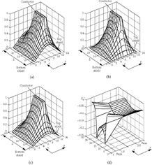
FIGURE 7.6
Distributions of potentials at (a) θ = 0, (b) θ = π, (c) θ = π/2, and (d) distribution of the modulus of the transverse component Eym at θ = π/2 in three longitudinal sections.
2. Calculation of potentials of the nodes at selected values of θ according to Equation ((7.24)). Distribution of potentials at θ = π/2 is presented in Figure 7.6(c).
3. Calculation of the distribution of the transverse component of the electric field according to Equation ((7.25)). Figure 7.6(d) illustrates the distribution of the component at conductors of the line, in the middle between the conductors and upper shield, and at the upper shield (at y = ymin, y = ymin + ymax/2 and y = ymax according to Figure 7.7).
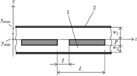
FIGURE 7.7
The fragment of the shielded one-row multiconductor line. 1: Conductor; 2: shield.
4. Calculation of the strength of the zero component Ey0m of the deflecting field at selected values of phase angle θ and transverse coordinate y according to Equation ((7.27)).
5. Calculation of coefficient
(7.28) |
where Em = Um/w is the strength of the deflecting electrical field in the electrostatic deflecting system of the same length as the electrodynamical system at um = 1 V; w is the gap between the deflecting electrodes.
Characteristic KE(θ) characterizes how the strength of the deflecting electrical field in the deflecting system depends on phase angle 8 and frequency.
Characteristics KE(θ), obtained using models presented in Figures 7.5 and 7.7, are presented in Figures 7.8 and 7.9. Curves 1 and 2 are plotted using Equations ((7.11)) and ((7.17)); curves 3–5 represent the results obtained using the numerical finite difference method.
The curves in Figure 7.8 characterize the system containing the slow-wave deflecting electrode whose conductors are relatively thick, and the gaps among them are relatively small. In this instance, the strength of the deflecting field in the middle between conductors and the shield obtained using the finite difference method practically coincides with the results obtained using analytical methods.
Figure 7.9 characterizes the system with thin conductors and relatively great gaps among them. In this instance, the results obtained using the finite difference method differ considerably from the results obtained using analytical methods. Even at small values of phase angle θ (in the low-frequency range), the real strength of the deflecting field is more than 20% less than that obtained using analytical methods.
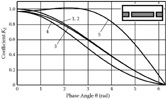
FIGURE 7.8
Characteristics KE(θ) at L = 2.2,l = 0.2, w1 = 1, p = 0.4 mm, and various values of coordinate y: y = (ymin + ymax)/2 (curves 1-3); y = ymin (curve 4); y = ymax (curve 5).
It is also important that the strength of the deflecting field greatly depends on phase angle and frequency. Because of the surface character of the field in the slow-wave structure, it also greatly depends on coordinate y. The strength is maximal at the surface of the slow-wave deflecting electrode and minimal at the shield.
The numerical method allows examination of the deflecting field in systems with complicated cross sections. Calculation results of the deflecting electrical field in an ordinary helical deflecting system and more complex gutter-type deflecting system (Figure 7.11) are presented in Figure 7.10. According to this figure, the strength of the deflecting component ε0 in the gutter-type system in the low-frequency range is less than in the ordinary helical system. At the same time, it is important that the field in the gutter-type system is less dependent on frequency. The last property of the gutter-type system is also its important advantage.
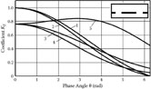
FIGURE 7.9
Characteristics KE(θ) at L = 2.2, l = 1.1, w1 = 1, p = 0.4 mm, and various values of coordinate y: y = (ymin + ymax)/2 (curves 1-3); y = ymin (curve 4); y = ymax (curve 5).
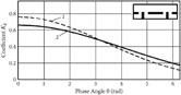
FIGURE 7.10
KE(θ) at the middle between the deflecting electrode and the shield in a simple helical system (curve 1) and gutter-type system (curve 2) at L = 2.2, w1 = 1,p = 0.1,L-l = a=1.1 and thickness of the shielding wall in the gutter-type system t = 0.1 mm.
7.2.4 Electric Field in a Twined Helical Deflecting System
General properties of the twined helical system were examined in Chapter 3. According to analysis, the twined helical deflecting system has no advantages with respect to ordinary helical systems. But according to the description of invention [19], the strength of the longitudinal component of the electric field in the twined helical system is small, and this ensures better focusing of the electron beam.

FIGURE 7.11
The fragment of the longitudinal section of a gutter-type multiconductor line. 1: Conductor of the line; 2 and 3: shields; 4: shielding wall.
FIGURE 7.12
Fragment of a one-row multiconductor line with two conductors in the period.
Let us examine the field in the twined helical system and compare it with the same component in an ordinary helical system.
Analyzing the electrical field, we can model helical deflecting systems by the one-row multiconductor line (Figure 7.12) [10], containing two conductors in the period of a system. In ordinary helical systems, the phase difference between voltages or currents on neighboring conductors in the row is θ; in the twined helical system, it is (θ + π). Considering one period of the systems model in the range 0 ≤ z ≤ zmax and using the finite difference method, we can find the potential distribution in the ordinary helical system, assuming that voltages on neighboring conductors are ejθ, 1, and e-jθ. In the twined helical system, the voltages are given by ejθ, -1, and e-jθ. Figure 7.13 illustrates potential distributions in the ordinary and twined systems.

FIGURE 7.13
Potential distributions in (a) ordinary and (b) twined helical systems at θ = 0.
At known potentials, we can find the transverse component of the electrical field using Equation ((7.25)). The longitudinal components of the field are given by
(7.29) |
where .
Distributions of the transverse component Eym and longitudinal component Ezm in the space between the helical conductors and the shield (in the range from y2 to ymax, according to Figure 7.12) are presented in Figure 7.14.
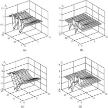
FIGURE 7.14
Distributions of (a, c) transverse and (b, d) longitudinal components of the electric field in (a, b) ordinary and (c, d) twined helical systems in the range from y2 to ymax at θ = 0.
The action of the longitudinal component on the electron beam can be evaluated by coefficient Kz = Ez0m/Em, where is the zero spatial component of the longitudinal component given by a formula similar to Equation ((7.27)):
(7.30) |
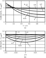
Figures 7.15 and 7.16 illustrate how deflecting components Ey0m in the ordinary and twined helical systems at y = (y2 + ymax)/2 depend on phase angles between voltages on neighboring conductors at various values of the neighboring conductors’ width ratio s = b/a = 2z1/(z3 - z2). Values of ratio θ/π and θ/2π plotted along axes of abscissas correspond to the same frequency values.

FIGURE 7.15
Coefficients Kz versus relative values of phase angle 8 for (a) ordinary and (b) twined helical systems at z2 -z1 = z4-z3 = 16Δ, zmax =232Δ, y1 =16Δ, ymax= 60Δ, and various values of ratio s. 1: 2 z1 = b = 100Δ, z3-z2 = a 100Δ, s = 1; 2: b = 120Δ, a = 80Δ, s = 1.5; 3: b = 140Δ, a = 60Δ, s=. 2.3; 4: b = 160Δ, a = 40Δ, s = 4. Here, Δ is the step of the nodes of the grid (when the finite difference method is used).
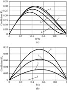
FIGURE 7.16
Coefficients Kz versus relative values of phase angle θ for (a) ordinary and (b) twined helical systems at z2-z1 = z4-z3 = 16Δ, zmax = 232Δ, y1 = 16Δ, y2 = 20Δ, ymax = 60Δ, and various values of ratio s. 1: 2z1 = b = 100Δ, z3 -z2 = a = 100Δ, s = 1; 2: b = 120Δ, a = 80Δ, s = 1.5; 3: b = 140Δ, a = 60Δ, s = 2.3; 4: b = 160Δ, a = 40Δ, s = 4. Here, Δ is the step of the nodes of the grid (when the finite difference method is used).
According to Figure 7.15(a), the strength of the deflecting field in the ordinary helical system in the low-frequency range at small gaps among the conductors is practically the same as in an electrostatic system. Because of the transit effect [4,5], the strength of the zero harmonic Ey0m decreases with θ and frequency. At higher values of ratio s, the change of Ey0m with θ is greater because the transit time over the conductor with width b (Figure 7.12) is greater.
According to Figure 7.15(b), at the same widths of the conductors, the strength of the deflecting field in the twined helical system is zero because the directions of the component are opposite and they cause deflection of the beam in opposite directions. With an increase of ratio s, the strength of the deflecting field in the twined helical system increases. On the other hand, it is important that coefficient Ky, is only about 0.5 at a relatively great ratio s. Thus, sensitivity of the tube with the twined system is considerably less.
If paraphase signals are used for deflection of the beam, symmetrical helical systems are planar symmetrical helical structures. Then, at the symmetry plane, the strength of the longitudinal electric field is zero in both types of the considered deflecting systems. With an approach to deflecting electrodes, the strength of the longitudinal component increases.
Figure 7.16 illustrates how coefficient Kz and longitudinal components of the field in the ordinary and twined helical systems depend on the relative value of phase angle θ at y = (y2 + ymax)/2. According to Figure 7.16(a, b), the strength of the longitudinal components at θ = 0 is zero. Coefficient Kz and the strength of the longitudinal component increase with θ and become maximal at θ ≅ π in ordinary helical systems and θ ≅ π/2 in twined helical systems. Maximal values of Kz depend on the type of deflecting system and conductor width ratio s.
According to Figure 7.16(a), in the ordinary helical system, coefficient Kz is maximal at the same widths of neighboring conductors (at s = 1). An increase of ratio s causes a decrease of the maximal value of Kz.
According to Figure 7.16(b), values of Kz and the strength of the longitudinal component in the twined helical system at s = 1 really are zero. This property of the deflecting system has been interpreted as an important advantage of the system [6]. Unfortunately, at a = b and s = 1, deflection of the beam is impossible because Ey0m = 0. If the ratio s increases, coefficient Kz also increases. According to calculations, at great ratio s, values of the ratio Kz/Ky = Ez0m/Ey0m are close to that in ordinary helical deflecting systems containing two separate helical electrodes. Thus, the idea about a small longitudinal electric field in the twined helical system is false.
Finally, it is important to notice that the properties of ordinary symmetrical and asymmetrical helical deflecting systems are not the same. In the symmetrical system, the initial position of the electron beam is at the center of the system (at y = ymax, according to the model in Figure 7.12), where the longitudinal component is zero. In an asymmetrical system, the initial position of the beam is at the center of the space between the slow-wave electrode and the shield (at y = (y2 + ymax/2)). In addition, the distance between the deflecting electrode and the electrical wall in the center of the symmetrical system is two times less than the distance between the slow-wave electrode and its shield in an asymmetrical system. For these reasons, the levels of the longitudinal field in an ordinary symmetrical deflecting system are less than in asymmetrical systems.
7.3 Nonlinear Distortions in Traveling-Wave Cathode-Ray Tubes
As the strength of the deflecting field becomes dependent on the transverse coordinate with an increase of the frequency, nonlinear distortions of the form of the signal on the screen of the tube arise. Also, problems related to electron beam focusing quality appear.
Let us consider peculiarities of frequency-dependent nonlinear distortions and possibilities to reduce these distortions and to improve focusing quality.
According to Figure 7.8, at l/L ≤ 0.1 and p/L ≥ 0.2, calculation results of the strength of the deflecting field, obtained using electrodynamical, multiconductor lines and finite difference methods, are practically the same. Additional analysis shows that analytical methods can be used if l/L > 0.25 and p/L > 0.1. Therefore, analytical methods are used for calculation of the deflecting field in Staras and Burokas [11,12] in order to simplify analysis of nonlinear distortion in a TW CRT containing an ordinary helical deflecting system (Figure 7.17).
The coordinate system is changed in Figure 7.17 with respect to Figure 7.5. Then the expression for the deflection field can be rearranged to
(7.31) |
where θ = ωτ, τ = L/vph, and τ is the transit time of the period of the deflecting system by electrons at matched velocity of electrons to the phase velocity of the deflecting wave.
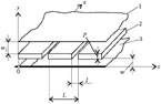
FIGURE 7.17
The fragment of the multiconductor line modeling helical deflecting system. 1 and 3: Shields; 2: conductor of the multiconductor line.
In the general case, all components of the electrical field act on the electron beam. At the same time, it is important that the intensity of component Ex can be reduced and eliminated with the correct selection of direction of conductors in the deflection area. The influence of the longitudinal component Ez is small because this component is considerably less than the strength of the accelerating electrical field in the TW CRT. Taking this into account, the influence of components Ex and Ez can be neglected.
We can find the deflection of the electron beam on the screen of the tube by solving [20]
(7.32) |
where e is absolute value of electronic charge and m is the electron’s mass.
7.3.1 Distortions of Harmonic Oscillations in Asymmetrical Helical Systems
In the case when the strength of the deflecting field depends on the coordinate, we can find the deflection of the beam on the screen assuming that (1) the deflecting system consists of N elementary parts, and (2) the displacements of the beam in the elementary part are small and variation of the deflecting field at deflection in the elementary part can be neglected. It is reasonable to relate the number of elementary parts to the number of conductors in the deflection area.
With the described conditions, we find the deflection of an electron of the beam on the screen of the tube, using the algorithm:
1. Taking into account the instantaneous value of deflecting voltage and initial coordinate y0 of an electron, we find the strength of the deflecting field acting on the electron, using Equation ((7.31)).
2. We find the transverse velocity and displacement of the electron in the first period of the deflecting system, using Equation ((7.32)).
3. Taking into account the initial coordinate of the electron and its displacement in the first period, we calculate the initial coordinate of the electron in the next period and the strength of the deflecting field using Equation ((7.31)). After that, we find the transverse velocity and the displacement of the electron in the period, using Equation ((7.32)).
4. We continue calculations up to the end of the deflecting system and find the total values of the transversal velocity vΣ and displacement yΣ.
5. At known values of vΣ and yΣ, the deflection of the beam on the screen of the tube is given by
(7.33) |
where
te = le/ve is the transit time of the electron from the end of the deflecting system to the screen of the tube
le is the distance of the screen from the end of the system
ve is the velocity of the electron dependent on accelerating voltage U0
In the application of the described algorithm,
(7.34) |
and
(7.35) |
where
(7.36) |
and
(7.37) |
In Equations ((7.32))–((7.35)), vi is the transversal velocity obtained by the electron in the ith part of the deflecting system and Δyi is the displacement in the ith part.
In an asymmetrical helical deflecting system, the beam is transmitted in the space between the helix and the shield below helical conductors. Let us assume that, according to Figure 7.17, the initial coordinate of an electron in the beam is y0 = w/2. Then, at positive values of deflecting voltage, deflection causes the approach of the beam to the slow-wave electrode, where the intensity of the deflecting field at high frequency is higher. Negative values of deflecting voltage cause downward deflection. The beam approaches the shield, where intensity of the deflection field at high frequency is less. As a result, frequency-dependent nonlinear distortions of the image on the screen of the tube appear.
The thin line in Figure 7.18 illustrates the waveform on the screen of the tube at the harmonic form of deflecting voltage when the deflecting field does not depend on the transverse coordinate and is given by um sin(2πt/T)/w.

FIGURE 7.18
Calculated waveforms on the screen of the tube at θ = π, L = 2.2, l = 0.2, w = 1 mm, N = 20, U0 = 1.5 kV, and le = 0.2 m.
The thicker line represents the distorted waveform due to frequency and the coordinate-dependent deflecting field. Ratio H/2A is plotted along the ordinate axis of the graph where 2A is the useful scan in the vertical direction; it is calculated assuming that the displacement of the considered electron at the end of the deflecting system at low frequency equals half of the gap w between the deflecting electrons (Figure 7.17).
Nonlinear distortions, of course, depend on the amplitude and frequency of deflecting voltage. At the same time, it is important that nonlinear frequency-dependent distortions do not appear even at maximal deflecting voltage amplitude (corresponding to maximal scan on the screen) if frequency is low. At this amplitude of deflecting voltage, distortions increase with an increase of phase angle θ and frequency. On the other hand, at great values of θ, distortions decrease because of decreasing sensitivity of the tube and decreasing displacement of deflected electrons in the slow-wave deflecting system. With a small deflection, the deflecting field acting on an electron of the beam remains almost constant. The curves presented in Figure 7.19 confirm this idea. Maximal deflections of the beam on the screen of the tube corresponding to the maximal instantaneous values of the maximal deflecting voltage versus phase angle θ are also presented in this figure.
A nonlinear distortion coefficient is used in practice to describe the level of nonlinear distortions. According to the nature of nonlinear frequency-dependent distortions, the second harmonic of the waveform determines the level of the distortions, and the nonlinear distortion coefficient is given by
(7.38) |
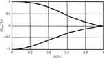
FIGURE 7.19
The maximal deflections of the beam on the screen at maximal amplitude of harmonic deflecting voltage versus phase angle θ at L = 2.2, l = 0.2, w = 1 mm, N = 20, U0 = 1.5 kV, and le = 0.2 m.
where H+ is the maximal deflection of the beam in the y direction on the screen, and H- is the maximal deflection in the opposite direction (H+ corresponds to Um and H- corresponds to -Um).
Figure 7.20 illustrates how the nonlinear distortion coefficient depends on phase angle θ at a constant amplitude of deflecting voltage.
The cross-section dimensions of the electron beam in a deflecting system are not infinitely small. For this reason, the intensity of the deflecting field is dependent on the transverse coordinate of an electron of the beam, and displacements of electrons are not the same. As a result, defocusing of the beam increases with frequency. The waveforms on the screen corresponding to initial coordinates y0 = w/4 and y0 = 3w/4 of electrons are presented in Figure 7.21. Figure 7.22 illustrates how defocusing of the beam depends on phase angle θ.

FIGURE 7.20
Nonlinear distortion coefficient versus phase angle θ at L = 2.2,1 = 0.2, w = 1 mm, N = 20, U0 = 1.5 kV, and le = 0.2 m.
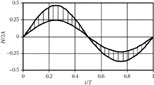
FIGURE 7.21
The waveforms on the screen at θ π, y0 = (1…3)w/4, L= 2.2, l =0.2, w = 1 mm, N = 20, U0 = 1.5 kV, and le = 0.2 m.
According to analysis, the surface character of the deflecting field in asymmetrical helical systems can cause considerable nonlinear distortions and defocusing in traveling-wave tubes. In Kocimski [21], only secondary effects are taken into account in the analysis of distortions and defocusing.
7.3.2 Reduction of Nonlinear Frequency-Dependent Distortions
We can reduce nonlinear frequency-dependent distortions and improve the quality of focusing inhibiting the surface character of the deflecting field, thus decreasing the cross-section dimensions of the slow-wave deflecting system and decreasing its retardation factor. Unfortunately, at small dimensions, precise manufacturing becomes complicated. Additionally, decreasing the gap between deflecting electrodes causes a decrease of the useful scan area on the screen. Decreasing the retardation factor necessitates increased accelerating voltage. This causes decreased sensitivity of the tube.
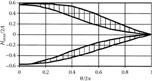
FIGURE 7.22
Scattering of maximal deflections of electrons on the screen due to the surface character of the deflecting field at y0 = (1…3)w/4, L = 2.2, l = 0.2, w = 1 mm, N = 20, U0 = 1.5 kV, and le = 0.2 m.
The surface character of an electromagnetic field in helical and meander systems develops with an increase of phase angle θ and strengthening of the electric field among neighboring conductors of slow-wave electrodes. According to Section 7.4, we can reduce the coupling between neighboring conductors using shielding walls. Thus, gutter-type systems and systems containing shielding walls connecting internal and external shields with holes for electron beams in the shielding walls [22,23] really are the most promising deflecting systems for super-wide pass-band TW CRTs.
Construction of symmetrical deflecting systems is more complicated with respect to asymmetrical systems. For this reason, asymmetrical systems are used in high-speed oscilloscopes and TW CRTs [24]. On the other hand, symmetrical systems have important advantages. We must take into account that, analyzing a symmetrical system in the case of the odd wave, we can divide the system by electrical wall into two asymmetrical systems [5,25]. Then the distance between slow-wave electrodes and the wall is two times less than the distance between deflecting electrodes. Additionally, it is important that the strength of the deflecting field acting on the electron beam in the symmetrical system corresponds to the strength at the electric wall. Considering the deflecting field, we must take into account the noted circumstances.
FIGURE 7.23
Distribution of the strength of a deflecting electrical field in (a) asymmetrical and (b) symmetrical helical systems at an increase of phase angle when L = 2.2, l = 0.6, w =1.5 mm in the asymmetrical system, and 2w = 1.5 mm in the symmetrical system.
7.3.3 Distortions of Electrical Pulses
Transient responses are used to characterize frequency distortions of pulse signals. The transient response of a quadripole is given by [26]
(7.39) |
where K(ω) and φ(ω) are amplitude-frequency and phase-frequency responses, respectively, of the quadripole.
In the case of the traveling-wave tube, we must take into account that the electric field, acting on an electron of the beam and the amplitude-frequency response of the tube, becomes dependent on the transverse coordinate and the trajectory of the beam.
Figure 7.23 illustrates distributions of the deflecting field in asymmetrical and symmetrical helical systems. According to this figure, the strength of the deflecting field in the symmetrical system changes, with θ considerably slower than in an asymmetrical system. At θ = π, the strength of the deflecting field in the space between deflecting electrodes of an asymmetrical system changes about 4.3 times. In the symmetrical system, it changes only 1.6 times.
In order to reveal the influence of the surface character of the deflecting field, let us not take into account attenuation, reflections, and other factors. Also, let us think that longitudinal velocity ve of electrons is matched with the phase velocity vph of the electromagnetic wave in the deflecting system (i.e., ve = vph). With these simplifications, the transfer function of the traveling-wave tube is given by
(7.40) |
where
(7.41) |
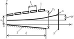
FIGURE 7.24
The model of the asymmetrical traveling-wave deflecting system. 1: Deflecting electrode; 2: shield (the second deflecting electrode in the symmetrical deflecting system); 3: screen of the tube; 4: electron beam.
and
(7.42) |
According to Equations ((7.40))–((7.42)), the transfer function of the tube is dependent on the transverse coordinate y. In addition, in the general case, when the distance between the deflecting elements changes along the system, the deflecting field is dependent on the longitudinal coordinate. Taking this into account, we can find the deflection of the beam on the screen of the tube considering the periodic slow-wave deflecting system as the system consisting of N pairs of elementary deflecting plates (Figure 7.24). In the elementary system, the change of the distance between the deflecting plates is small, the change of the transverse coordinate of an electron is small, and the strength of the deflecting electrical field does not depend on coordinates. The transverse velocity of an electron of the beam and its deflection in the elementary deflecting system can be found by solving Equation ((7.32)).
With the mentioned simplifications, we can find the deflection H(t) on the screen and the transient response T(t) of the tube acting in this way:
1. At the known transverse coordinate y = w1 of an electron at the input of the deflecting system, the transfer function of the first elementary deflecting system is found using Equation ((7.40)).
2. The value of the transient response T1(t1) of the first elementary deflecting system is determined using Equation ((7.39)). Here, t1 is time with respect to the unit step of the probing voltage.
3. At known T1(t1) and known height of the probing voltage step, the transverse velocity v1(t1) and the displacement Δy1(t1) at the end of the first elementary system are found by solving Equation ((7.32)).
4. The transverse coordinate and the transverse velocity of the electron of the beam at the input of the second elementary system are determined.
5. Steps 1–4 are repeated for other elementary deflecting systems. As a result, the total displacement of the electron ΔyΣ(t1) and the total transverse velocity vΣ(t1), obtained by the electron in the traveling-wave deflecting system, are determined.
6. The deflection of the electron that entered the deflecting system at time moment t1 is determined:
(7.43) |
Here, te is the transit time of the electron from the end of the deflecting system to the screen of the tube.
7. Steps 1–6 are repeated for other time values t1.
8. The normalized transient response of the tube is determined:
(7.44) |
where H0 is the deflection of the beam on the screen, caused by the direct voltage, equal to the height of the probing step.
The initial trajectory of an electron can be different from the middle of the gap between the deflecting electrodes. Also, the direct bias voltage can be used. Thus, the trajectory of the electron in the traveling-wave deflecting system in the absence of the probing step can generally be described by
(7.45) |
where a and b are coefficients.
Selecting values of a and b, we can simulate various initial trajectories of electrons and take them into account, calculating values of deflection and transient response.
The transient responses of the tube at linear initial trajectory (b = 0) and a small height of the probing voltage step are presented in Figure 7.25. The initial trajectory is determined by the transverse coordinates y01(at the input) and yout = y0(ls) (at the end) of the system.
According to Figure 7.25(a), the slope of the transient response of the tube with the asymmetrical deflecting system is the best and the rise time is minimal when the initial trajectory is at the slow-wave electrode. Unfortunately, short, quick increases of deflection before and after the front exist.
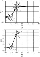
FIGURE 7.25
Transient responses of the tubes with (a) asymmetrical and (b) symmetrical traveling-wave deflecting systems at small heights of probing voltage steps at w1 = 1, w2 = 3, L = 1.5 mm, N = 10, U0 = 1.5 kV, le = 0.15 m. 1: y01= 0.1 w2;2: y01 = 0.1 w2; 2: y01 = 0.3 w1 y01 = 0.3 w2; 3: y01 = 0.5 w1 yout = 0.5 w2 4: y01 = 0.7 w1, yout = 0.7 w1 5: y01 = 0.9 w1 yout = 0.9 w2.
The deflecting field in the symmetrical system does not change if the electrical wall is placed in the middle of the gap between the slow-wave electrodes. Thus, the properties of the symmetrical deflecting system are the same as the properties of the asymmetrical deflecting system, with the distance between the deflecting electrodes two times less. For this reason, the influence of the surface character of the field on the transient response of the tube with the symmetrical deflecting system is less (Figure 7.25b).
If the gaps between deflecting electrodes are the same in symmetrical and asymmetrical deflecting systems and the trajectory of the beam is at the middle of the gap, the electric fields, acting on electrons, according to Equation ((7.42)), are the same in symmetrical and asymmetrical systems, and their transient responses at a small height of the probing voltage coincide.
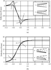
FIGURE 7.26
Transient responses of the tube with the asymmetrical deflecting system at (a) negative and (b) positive probing steps w1 = 1, w2 = 3, L = 1.5 mm, y01 = 0.5 w1 N = 10, U0 = 1.5 kV, le = 0.15 m. 1, 2: yout = 0.9 w2 3, 4: yout = 0.1 w2.
The waveforms on the screen of the tube in the case when the beam enters the system at the middle between deflecting electrodes (at y01 = 0.5 w1) and high steps of deflecting voltage are presented in Figure 7.26. Curves 1 and 3 are obtained at linear initial trajectories of the beam (at b = 0), and curves 2 and 4 are obtained in the case when the maximal direct bias voltage is used and the initial trajectory is of the form of a parabola.
According to Figures 7.25 and 7.26(a, b), the transient response of the traveling-wave tube with the asymmetrical deflecting system is dependent on the initial trajectory, bias voltage, polarity, and height of the probing step. With a positive voltage step, the slope of the front is less, and the rise time of the response is greater than in the case of the negative voltage step. Additionally, we see that the slope and the rise time depend on the initial trajectory of the beam. At the positive voltage step, the rise time is less if the initial trajectory is parabolic (i.e., if constant bias voltage is used), but at the negative step, the rise time is less at the linear initial trajectory.
In the case of a symmetrical deflecting system, the slope and rise time of transient responses do not depend on the polarity of the probing step.
More detailed information about distortions of pulse signals is presented in references 11, 12, and 27. Analysis confirmed that distortions of pulse signals, like distortion of harmonic oscillations, can be reduced by inhibiting the surface character of the deflecting field.
7.4 Simulation of Transitions to Traveling-Wave Deflecting Systems
Transitions with the pass-band from 0 to some gigahertz are necessary for modern TW CRTs. The ideal field patterns of slow-wave structures are distorted at their ends. As a result, end capacitances and discontinuities of the circuits appear, limiting the pass-band of the circuits and devices containing slow-wave structures. According to experimental investigations and modeling [4,5,28,29], narrowed turns and increased gaps between slow-wave electrodes and shields at the ends of the electrodes allow reducing reflections from the ends of the systems and improving the transfer characteristics of the circuits containing the systems.
Various models and methods were developed for analysis of transitions between different types of transmission lines and waveguides. On the other hand, the question about the influence of transitions in the case of TW CRTs is specific because the dynamic characteristics of TW CRTs, characterizing image form distortions on the screen, differ from the dynamic characteristics of signal paths, which characterize transfer of signals to the load resistance of the signal path in the tube.
New opportunities of modeling and investigating transitions to slow-wave structures appear when numerical methods are applied [30,31].
Taking this into account, let us compose the equivalent circuit of the deflection path containing the deflecting system and consider the responses of the TW CRT and the deflection path in order to reveal peculiarities of operation of the transitions to the helix. Simulation of the transitions will allow grounding the ways that improve transfer of signals to the deflecting system and lead to better dynamic characteristics of traveling-wave cathode-ray tubes.

FIGURE 7.27
Fragments of (a) longitudinal and (b) cross sections of the helical deflecting system. 1: Helix; 2: end wire; 3: internal shield; 4: external shield; 5: diaphragm; 6: strip line.
7.4.1 Model of the Deflection Path
Let us consider the deflection path containing the helical deflecting system (Figure 7.27). The system consists of a helix and shields. The terminals of the system have the form of the strip lines.
The segment of the shielded multiconductor line (Figure 7.28a), containing a row of conductors and a conductor in a period, can be used to model the helical deflecting system. The cross section of the strip line is presented in Figure 7.28(b). Because of electrical field spread in the cross section of the strip line, less width of a conductor is necessary to obtain a particular characteristic impedance.
At the end of the helix (Figure 7.28c), one side of the conductor is in conditions similar to the conditions in the multiconductor line. The distribution of the field on the external side of the conductor is similar to that in the strip line. Because of the spread of the field at the end, the wires with less width (d1 < d2 < d) are used at the ends of the helix. They act as transitions to the helical deflecting system.
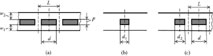
FIGURE 7.28
Cross sections of the lines, modeling the sections of the deflection path.
The elements of the deflection path of the traveling-wave cathode-ray tube are in a vacuum. Then, the flattened shielded helical system is practically nondispersive. Its characteristic impedance is given by
(7.46) |
and
(7.47) |
We used the finite difference and finite element methods for calculation of characteristic admittances ϒc(0), ϒC(π) of the multiconductor line (Figure 7.28a) and characteristic impedance Zcs of the strip line (Figure 7.28b). Calculating the impedance of the transitions, we considered one-half of the end wire (Figure 7.28c) as a half of the strip line (width of conductor d2), and the other half as a half of a period of the multiconductor line. With these conditions, the characteristic impedance of transitions is given by
(7.48) |
and
(7.49) |
where ϒCSt and ϒCt(θ) are characteristic admittances of the strip line and multiconductor line at width d2 of the conductor in the transition section (Figure 7.28c).
Calculation results for the signal path with a characteristic impedance of 100 Q are presented in Table 7.1 and Figure 7.29. In order to have the generalized graph, ratio θ/π is plotted along the x axis in Figure 7.29. The phase angle θ is related to frequency f by
(7.50) |
TABLE 7.1
Characteristic Impedances of the Signal Path
Element |
Width of conductor (d, d1, d2)/mm |
Z(0)/Ω |
Z(π)/Ω |
Helical system |
1.5 |
100.6 |
37.3 |
Strip line |
0.6 |
99.1 |
99.1 |
End wire |
1.5 |
80 |
47.7 |
End wire |
0.6 |
129 |
59.6 |
End wire |
1 |
101 |
53.6 |
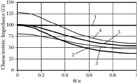
FIGURE 7.29
Characteristic impedances of the deflection path elements versus relative values of phase angle θ at L = 2, w1 = 1, w2 = 1.07, p = 0.5, l = 0.5(L -d) = 1.5 mm. 1: Strip line; 2: helical system; 3, 4, 5: end wires at d2 = 1.5, 0.6, and 1 mm, respectively.
where lt is the length of the helical turn and kR ≅ It is the approximate value of the retardation factor.
The equivalent circuit of the deflection path is presented in Figure 7.30(a). It consists of segments of strip lines, a helical line, and segments of the lines, modeling the transitions (narrowed end wires of the helix).
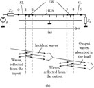
FIGURE 7.30
(a) Equivalent circuit of the deflection path and (b) the diagram of multiple reflections. SL: The segment of the strip line; HDS: helical deflecting system; EW: end wire.
Using a multiple reflections diagram (Figure 7.30b) like that used in references 4 and 5 and taking into account reflection from inhomogeneities at the beginning of the signal path (at points 1 and 2), we derive this expression for the reflection coefficient:
(7.51) |
where
(7.52) |
Here, p1 and p2 are reflection coefficients at points 1 and 2, respectively, and t12 is the delay time in the section of the deflection path between points 1 and 2.
Then the transfer function characterizing the transmission of signals from source E to the input of the deflecting system is given by
(7.53) |
If reflections from inhomogeneities at the end of the deflecting system are taken into account, the expression of the transfer function characterizing frequency distortions at the input becomes
(7.54) |
(7.55) |
(7.56) |
and
(7.57) |
where
t23 is the delay time in the deflecting system (between points 2 and 3)
is the reflection coefficient from the end of the deflecting system (from points 3 and 4)
t34 is the delay time in the section of the deflection path between points 3 and 4
is the reflection coefficient of the reflected wave (propagating in the -x direction in the deflecting system) from the input end of the system
When only incident waves are taken into account, the transfer function characterizing transmission to the end of the deflecting system is given by
(7.58) |
and
(7.59) |
Taking into account secondary incident waves (reflected from inhomogeneities at the input), we can derive the expression for the transfer function characterizing transmission to the end of the deflecting system:
(7.60) |
In Equations ((7.51))–((7.60)), p1 p2 p3 and p4 are reflection coefficients (for the incident waves) at points 1-4:
(7.61) |
(7.62) |
(7.63) |
(7.64) |
Applying Equations ((7.51))–((7.64)) in order to reveal the influence of transitions on the dynamic characteristics of the deflecting system and TW CRT, let us assume that the internal impedance of the signal source and the load impedance are matched with characteristic impedances of the strip lines.
Amplitude-frequency responses characterizing frequency distortions in the deflection path and TW CRT are presented in Figure 7.31(a–e). Curves 1 and 2 are obtained using Equations ((7.58)) and ((7.60)), and curves 3 and 4 are obtained using Equations ((7.53)) and ((7.54)). Thus, characteristics 1 and 3 do not take into account secondary incident waves appearing as a result of reflections from the output and input of the deflecting system. Due to these waves, oscillations on amplitude-frequency characteristics appear with an increase of θ and frequency (curves 2 and 4).
In the calculation of characteristics presented in Figure 7.31(a), assuming that Zct(θ) = ZCS, we did not take into account inhomogeneities due to transitions. Characteristics presented in Figure 7.31(b–d) are obtained at t12 = t34 = τ and different widths of end wires (d2 = 1.5,0.6, and 1 mm, respectively). Finally, the curve presented in Figure 7.31(e) characterizes frequency distortions at d2 = 1 mm and shortened transitions (t12 = t34 = τ/2).

FIGURE 7.31
Amplitude-frequency characteristics of the signal path (curves 1 and 2) and TW CRT (curves 3 and 4).
Comparing the presented amplitude-frequency responses, we see that characteristics of the signal path KOUT0 and KOUT Σ strongly depend on transitions. Using narrowed turns of the helix at its ends, we can effectively improve the frequency properties of the deflection path. This is in accordance with Skudutis and Daskevicius [31], where software package Microwave Office was used for analysis of the circuit containing a helical structure.
Additionally, it is important that responses KOUT0 and KOUT Σ strongly depend on the lengths of the transitions. At t12 = t34 = τ/2 (Figure 7.31e), variation of the amplitude-frequency responses KOUT0 and KOUTΣ is less than 10% in the range from 0 to θ = π, despite the fact that the characteristic impedance of the helical system at θ = π becomes about three times less with respect to its value at low frequency (Figure 7.29). We can explain this, considering the transition as the quarter wavelength matching transformer with frequency dependent characteristic impedance. Calculation of reflected signals confirms this idea.
The waveforms of reflected signals from the input of the deflecting system at probing voltage of the form of the unit step are presented in Figure 7.32. They are obtained using Equation ((7.51)) and the expression for transient response similar to Equation ((7.39)). In order to avoid oscillations of the transient response that appears due to limited upper limit of integration, the Bernstein-Rogosinski multiplier is used, as in Staras et al. [5].

FIGURE 7.32
Waveforms of reflected signals at ZCt(θ) = ZCS (curve 1); t12 = t34 = τ,d2 = 1.5,0.6, and 1 mm (curves 2–4); and t12 = t34 = τ/2, d2=1 mm (curve 5).
The waveforms in Figure 7.32 are obtained at the same conditions as the amplitude-frequency characteristics presented in Figure 7.31. According to waveforms of reflected signals, using narrowed turns at the ends of the helical deflecting system, we really can decrease the levels of reflected signals. The minimal values are obtained at t12 = t34 = τ/2 when narrowed sections (junctions) act as matching transformers at θ = π.
Unfortunately, the matching transformer at the input of the deflecting system can improve only power transfer. A decrease of the characteristic impedance of the helical system with frequency causes a decrease of the voltage on the element at constant power.
If we do not take into account attenuation, the amplitude of the incident wave does not change along the deflecting system. Thus, transfer functions and represented by curves 3 and 4 in Figure 7.31 determine frequency distortions of signals acting on electron beams in the deflecting system. According to Figure 7.31, amplitude-frequency characteristics and fall with 8 and frequency, and only slightly depend on transitions. The transient response T0(t) (Figure 7.33), corresponding to transfer function , also does not depend on transitions.
When we consider the distortions of signal shapes on the screen of the tube, in addition to and , we must take into account, at least, the transit time. The simplified expression for the transfer characteristic of the tube is given by
(7.65) |
where x ≅ ωτ/2.
Calculated transient responses of the TW CRT are presented in Figure 7.34.

FIGURE 7.33
Transient response corresponding to transfer function at ZCt(θ) = ZCS (curve 1); t12 = t34 = τ, d2 = 1.5, 0.6, and 1 mm (curves 2-4); and t12 = t34 = τ/2, d2=l mm (curve 5).

FIGURE 7.34
Transient responses of the TW CRT at ZCt(θ) = ZCS (curve 1); t12 = t34 =τ, d2 = 1.5, 0.6, and 1 mm (curves 2-4); and t12 = t34 = τ/2, d2 = 1 mm (curve 5).
Thus, according to analysis, transitions to helical deflecting systems operate as matching elements and allow improving the responses of the deflection path, but cannot improve dynamic properties of TW CRTs. On the other hand, analysis of the role of transitions leads to important recommendations for designers of TW CRTs: Deflecting systems with unchanging characteristic impedance are necessary for super-wide-band TW CRTs.
7.4.3 Reduction of Frequency Distortions
According to references 2–6, dispersion of phase velocity of a deflecting electromagnetic wave is the main factor limiting the pass-band of a TW CRT. The dispersion in helical deflecting systems is relatively small [5,6]. Unfortunately, variation of characteristic impedance in these systems is relatively great. For this reason, values of the transient response characterizing distortions of signals at the input of the deflecting system increase step by step (Figure 7.33). The height of the maximal step (at t ≅ 0) is given by [13]
(7.66) |
Thus, in order to improve the form of the transient response (increase B and reduce the heights of other steps), we must look at how to increase ZC(π) (decrease variation of characteristic impedance and achieve ZC(π) ≅ ZC(0)). Variation of characteristic impedance decreases with approaching shields to the helix and increasing gaps among helix conductors. Unfortunately, the approach of shields is followed by a fall of characteristic impedance, and an increase of gaps is followed by a decrease of sensitivity.
Meander systems have relatively constant characteristic impedance [4,5]. In the case of an ordinary meander system, the ratio of maximal (at θ = 0) and minimal (at θ = π/2) values of characteristic impedances is given by
(7.67) |
This ratio is considerably less than ratio ZC(0)/ZC(π) of ordinary helical systems. For this reason, using meander deflecting systems, we can obtain relatively good amplitude-frequency responses. Unfortunately, dispersion of phase velocity in meander systems is relatively great, and dynamic properties of tubes with meander systems are limited due to phase-frequency distortions.
In order to reduce the change of the characteristic impedance and the dispersion, we must reduce the coupling between the adjacent turns of the helix or meander electrodes. The additional shielding walls used between the turns (i.e., application of gutter-type helical and meander systems) helps to solve the problem effectively [5,22,23]. It is also important that usage of additional shielding walls helps to solve problems related to transitions because the additional spread of the field at the ends of the gutter-type systems practically does not exist.
Dynamic characteristics of TW CRTs and their signal paths depend on dispersion of deflecting electromagnetic waves, attenuation in the deflecting system, distribution of the deflecting electrical field, processes in transitions, and other factors [2,3,4,5,6,32]. On the other hand, researchers and designers sometimes represent characteristics of deflecting systems as characteristics of cathode-ray tubes [21,33]. This position is not correct.
Let us consider the influence of various factors on dynamic characteristics of signal paths and TW CRTs and reveal opportunities for improvement of dynamic properties in the case of helical deflecting systems.
In practice, dispersion of deflecting wave velocity and dispersion of delay time in the deflecting system are the main factors limiting the pass-band of the signal path and the TW CRT. The transfer function of a deflecting system is given by
(7.68) |
where td is the delay time in the system.
At the input of the deflecting system, the signal without phase-frequency distortions acts on the electron beam. As a result, phase-frequency distortions in the tube are less than in the deflecting system. On the other hand, if the phase velocity is frequency dependent, velocities of electrons in the beam can be matched in a limited frequency range, and amplitude-frequency distortions of the waveform on the screen appear. As a result, the transfer function of the tube is given by [3,4,5,6]
(7.69) |
where
(7.70) |
where
ts = ls/ve is the transit time
ls is the length of the deflecting system
ve is the velocity of electrons
Let us assume that the delay time is linearly dependent on frequency f:
(7.71) |
where t0 is the delay time at low frequency and S is the proportionality coefficient characterizing the slope of the characteristic td(f).
According to references 4 and 5, the change of the delay time in the pass-band of a TW CRT must not exceed 0.35 tr*, where tr* is the necessary rise time of the transient response of the tube (tr*≅ 0.35 / ΔFe*, where ΔFe* is the equivalent width of the pass-band of the tube).
Transient responses of the deflecting system and TW CRT are presented in Figure 7.35. In the calculation of the transient response of the cathode-ray tube, optimal accelerating voltage is selected to have the minimal rise time of the response.
If only dispersion is taken into account, according to analysis, the rise time of the transient response of the tube is related to the slope of characteristic td(f) by the following formula:
(7.72) |
Phase-frequency distortions in the deflecting system are greater. The rise time of the transient response of the system is about times greater than the rise time of the transient response of the tube
(7.73) |

FIGURE 7.35
Transient response of the deflecting system (curve 1) and the tube (curve 2).
According to references 4 and 5, the allowed variation of delay time in the deflecting system is to in the equivalent pass-band. Taking into account this condition, we can find that
(7.74) |
Then, according to Equations ((7.72))–((7.74)) and Figure 7.35, we have that the rise time trCRT1 of the transient response of the tube due to dispersion is about , and the rise time of the transient response of the deflecting system is about .
As was mentioned, with variation of wave velocity, matching of velocity of electrons with velocity of the wave is possible only at some frequencies. As a result, amplitude-frequency distortions of the waveforms on the screen arise. On the other hand, according to Staras and Burokas [16], variation of the amplitude-frequency characteristic practically has not influenced the rise time of the transient response of the tube if the velocity of electrons is optimal. Moreover, a downfall of the amplitude-frequency characteristic in the high-frequency range allows improvement of the transient response of the tube. Because of lesser levels of restored high-frequency spectrum components, oscillations of the transient response after its main step become less (Figure 7.35).
7.5.2 Influence of Attenuation
Because of attenuation, the transfer function of the deflecting system is given by
(7.75) |
where α is the attenuation coefficient and ls is length of the system.
Assuming that the attenuation coefficient linearly depends on frequency, we can show that the transient response corresponding to Equation ((7.75)) is given by
(7.76) |
where τs = kα l, kα is the proportionality coefficient (α = kαω).
We can derive expressions for the transfer function and the transient response of the tube by solving Equation ((7.32)). In the case when the displacement of electrons in the deflecting system is small and deflection of the beam on the screen is determined by the transverse velocity of the electron, the transfer function of the tube is given by
(7.77) |
In the frequency range where attenuation is small (αl ≪ 1), the expression for the transfer function can be simplified to
(7.78) |
Figure 7.36 illustrates influence of attenuation on the transient response of the deflecting system (curve 1) and the tube (curve 2). Calculations of transient responses are performed taking into account that, according to references 4 and 5, attenuation in the equivalent pass-band of the tube must be less than 2 dB. Then,
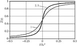
FIGURE 7.36
Transfer responses of deflecting system (curve 1) and tube (curve 2).
According to Figure 7.36, the rise time of the deflecting system is given by
(7.79) |
The rise time of the transient response of the tube is
(7.80) |
Thus, the rise time of the transient response of the tube is about two times less than that of the deflecting system.
We can rearrange Equation ((7.77)) in the form of the following series:
(7.81) |
where a= αl/2.
When the first two components of Equation ((7.81)) are taken into account, the transfer response is given by
(7.82) |
where τa = τs/2.
The transient response calculated using Equation ((7.82)) coincides with characteristics calculated using Equations ((7.39)) and ((7.77)). Thus, the formula in Equation ((7.82)) can be used as an approximation of the transient response of the tube in the analysis of attenuation onto dynamic properties of TW CRTs.
7.5.3 Influence of Characteristic Impedance Variation
According to analysis of helical systems, characteristic impedance of an ordinary helical system is the same as characteristic impedance of the multiconductor line if the systems is nondispersive.
The influence of characteristic impedance variation on properties of helical deflecting systems and cathode-ray tubes was considered in Section 7.4. Calculated transient responses of the deflecting system and tube are presented in Figure 7.37.
The transient response of the tube is of the form of some steps delayed by the transit time of a period by electrons. The heights of the steps depend on the ratio of characteristic impedances ZC(π) and Zc(0). According to Equation ((7.66)), the heights of the steps before and after the main step increase with a decrease of ZC(π)/ZC(0). The slopes of the steps are determined by the upper limit of integration at calculation of the transient response.

FIGURE 7.37
Transient responses of signal path (curve 1) and tube (curve 2) at nominal impedance of the path Zn = 100 Ω, ZCS(0) = 100 Ω, Zcs(p) = 37 Ω, ts/tt = N =10.
When other factors limiting the pass-band of the tube are taken into account, steps before and after the main step can increase the rise time of the response from level 0.1 to level 0.9. In Figure 7.37, the heights of the steps before and after the main step are about 0.1. Therefore, we can assume that the rise time of the transient response of the tube is approximately equal to the transit time τ.
The transient response of the signal path also contains steps. At the same time, it is important that the heights of the steps before and after the main step are small and practically do not affect the rise time of the response.
Thus, the variation of characteristic impedance of the deflecting system has essential influence on the transient response of the tube, but does not influence dynamic properties of the signal path. (By the way, according to Section 7.4, it is possible to improve dynamic characteristics of the signal path using properties of transitions acting as quarter-length transformers.)
It is also important to add that dynamic properties of signal paths and tubes are dependent on reactances at the input and the output of the deflecting system. Dynamic characteristics of the tube depend on reactances at the input, and dynamic characteristics of the signal path depend on reactances at the input and at the output.
The influence of a variation of characteristic impedance and reactances at the ends of the deflecting system can be reduced using gutter-type deflecting systems.
7.5.4 Influence of Peculiarities of a Deflecting Field
Evaluating the influence of a variation of a deflecting electrical field, we can use Equations ((7.9))–((7.11)), describing dependence of the strength of the field on frequency and the transversal coordinate.
According to Equations ((7.41)) and ((7.42)), at w = L, y = w/2, and θ = π, values of transfer functions K1(ω) and K2(ω) are practically the same. At lesser values of w, the influence of the surface character of the field is less than the influence of transit time τ.
Equation ((7.10)) describes the influence of the transit time on frequency properties of the tube. Taking into account the transit time, we can derive the expression for the transient response of the tube:
(7.83) |
where l(t) is the unit step (Heaviside) function.
The rise time of the transient response (Equation (7.83)) is
(7.84) |
At y = w/2, the transient response corresponding to the transfer function (Equation (7.10)) is given by
(7.85) |
Its rise time is
(7.86) |
At w ≤ L, we have that trCRT5 ≤ 0.7 τ. Figure 7.38 illustrates the forms of transient responses TCRT4(t) and TCRT5(t).
The presented information shows that, due to the transit effect and surface character of the field, the rise time of the transient response of the tube is approximately (0.8… 1.06) τ. According to references 4 and 5, the transit time τ must be to . Then we have that , and the rise time due to both considered effects can be evaluated using the following relationship: .

FIGURE 7.38
Transient response of the tube calculated taking into account transit effect (curve 1) and surface character of the deflecting field (curve 2).
In addition, it is important to notice that the surface character of the deflecting field in symmetrical systems is less expressed than in asymmetrical systems.
Finally, it is evident that the transit effect and surface character of the field do not influence the dynamic properties of the signal path.
7.5.5 The Conjoint Influence of Various Factors
Information presented in Table 7.2 characterizes the separate and conjoint influence of various factors on transient response rise time of the deflecting system and cathode-ray tube when requirements for the width of the equivalent pass-band of the TW CRT [4,5] are satisfied.
When all factors are taken into account, the rise time can be evaluated using
(7.87) |
Here, tri is the rise time due to the ith factor.
It is important that factors have different influences on the dynamic properties of signal paths and tubes. Analysis confirms that requirements for parameters of traveling deflecting systems formulated in references 4 and 5 are enough to ensure the necessary width of equivalent pass-band of the tube and the necessary rise time of its transient response.
According to analysis and data in Table 7.2, the rise time of the transient response of the signal path of the tube exceeds the rise time of the transient response of the TW CRT by about 1.3 times.
Dispersion of the delay time in the traveling-wave deflecting system really is the main factor limiting the operation speed of TW CRT. Usage of gutter-type helical and gutter-type meander systems can allow reducing dispersion, variation of characteristic impedance, reactances in the signal path, and downfall of the strength of the deflecting electrical field. Thus, gutter-type systems are the most prospective deflecting systems for TW CRTs.
TABLE 7.2
Influence of Various Factors on Rise Time of Transient Responses of Signal Path and TW CRT
Rise time of the transient response |
||
Factor |
Signal path |
TW CRT |
Dispersion of delay time |
1.12 tr* |
0.78 tr* |
Attenuation in deflecting system |
0.65 tr* |
0.32 tr* |
Downfall of characteristic impedance |
∼0 |
≤ 0.4 tr* |
Period transit time and surface character of deflecting field |
0 |
0.34 tr* |
Conjoint action of factors |
≈ 1.3 tr* |
≤tr* |
We showed that correction of phase-frequency distortions in traveling-wave oscilloscopes is possible. A correcting quadripole used before the traveling-wave deflecting system allows reduced distortions of waveforms on the screen of the tube. In addition, a better solution is possible. A deflecting system consisting of two parts with opposite dispersion characteristics can be used. Conditions for minimal distortions in the signal path differ from conditions for minimal distortions of waveforms on the screen.
We considered calculation methods of an electrical field in traveling-wave deflecting systems and revealed peculiarities of deflecting fields in various deflecting systems. As a result of the surface character of the electromagnetic field in slow-wave structures, the strength of the deflecting field is dependent on frequency and the transverse coordinate, and frequency-dependent nonlinear distortions appear and increase with frequency. We developed calculation methods of harmonic and pulse signal waveforms on the screen.
In order to reduce frequency-dependent distortions, we must decrease electromagnetic coupling between neighboring conductors of the slow-wave deflecting system. The coupling can be effectively reduced using additional shielding walls between neighboring conductors (i.e., using gutter-type deflecting systems). The strength of the deflecting field in symmetrical deflecting systems is less dependent on frequency with respect to asymmetrical systems. Twined helical deflecting systems have no preference with respect to ordinary helical systems.
We proposed the model of the signal path containing a helical deflecting system and revealed processes in transitions to deflecting systems. At downfall of characteristic impedance of a deflecting system, dynamic characteristics of the tube can differ considerably from the dynamic characteristics of the signal path. Transitions can act as quarter-wave transformers. Using their properties, we can realize matching of elements in the signal path and considerably improve its dynamic characteristics. Unfortunately, dynamic characteristics of the tube are determined by a variation of characteristic impedance of the deflecting system and only slightly depend on transitions. In order to reduce frequency distortions in the tubes, we must reduce the downfall of characteristic impedance. From this point of view, gutter-type deflecting systems are the best solution.
In order to reveal opportunities for improvement of dynamic characteristics, we examined the influence of various factors and the conjoint influence of these factors on characteristics of signal paths and tubes. According to analysis, factors have different influences on dynamic properties of signal paths and tubes. Analysis confirms that requirements in references 4 and 5 formulated for parameters of traveling deflecting systems are enough to ensure the necessary width of equivalent pass-band of the tube and necessary rise time of its transient response. The rise time of the transient response of the signal path of the tube exceeds the rise time of the transient response of TW CRT by about 1.3 times.
Dispersion of the delay time in the traveling-wave deflecting system really is the main factor limiting operation speed of the TW CRT. Usage of gutter-type helical and gutter-type meander systems can allow reducing dispersion, variation of characteristic impedance, reactances in the signal path, and downfall of the strength of the deflecting electrical field. Thus, gutter-type systems are the most prospective deflecting systems for TW CRTs.
1. Haeff, A. V. 1936. Device for the method of controlling high frequency current. US Patent No. 2064469.
2. Himmelbauer, E. E. 1969. Design considerations for a wide-band oscilloscope tube with scan magnification. Philips Research Reports supplements, no 1. 114 pp.
3. Shkunov, V. A. 1976. Wide-band oscilographic tubes and their applications. Moscow: Energy, 128. [In Russian.]
4. Vainoris, Z., Kirvaitis, R., and Staras, S. 1986. Electrodynamic delay and deflection systems Vilnius, Lithuania: Mokslas, 266. [In Russian.]
5. Staras, S. et al. 1993. Super-wide band tracts of the traveling-wave cathode-ray tubes. Vilnius, Lithuania: Technika, 360. [In Russian.]
6. Staras, S., and Skudutis, J. 1999. Traveling-wave deflection systems. Software for Electrical Engineering and Design, WITPRESS, Southampton. Boston, 23–32.
7. Staras, S. 2000. Models and simulation of traveling-wave deflection systems. Electronics and Electrical Engineering 2 (25): 23–29.
8. Staras, S., and Skudutis, J. 1996. Correction of phase-frequency distortions in oscillographic traveling-wave tubes. Electronics and Electrical Engineering 3 (7): 33–36. [In Lithuanian.]
9. Staras, S., and Kleiza, A. 2000. Analysis of electric field in the traveling-wave deflection system. Electronics and Electrical Engineering 1 (24): 12–15. [In Lithuanian.]
10. Staras, S., and Burokas, T. 2002. Electric field in helical traveling-wave systems. Electronics and Electrical Engineering 2 (7): 55–59. [In Lithuanian.]
11. Staras, S., and Burokas, T. 2003. Nonlinear distortions in traveling-wave deflection systems. Electronics and Electrical Engineering 6 (48): 42–47. [In Lithuanian.]
12. Staras, S., and Burokas, T. 2006. Frequency-dependent distortions of pulses in the traveling-wave cathode-ray tubes, Mikon 2006, XVI International Conference on Microwaves, Radar and Wireless Communications: Conference Proceedings, Krakow, Poland, May 22–24, 2:812–815.
13. Staras, S., and Skudutis, J. 1997. Input impedance of helical system. Radiotekhnika i Elektronika 42 (4): 395–397. [In Russian.]
14. Staras, S., and Burokas, T. 2004. Modeling and improvement of the traveling-wave deflection systems and their transitions. Electronics and Electrical Engineering 1 (50): 9–15. [In Lithuanian.]
15. Staras, S., and Burokas, T. 2004. Simulation and properties of transitions to traveling-wave deflection systems. IEEE Transactions on Electron Devices 51 (7): 1049–1052.
16. Staras, S., and Burokas, T. 2005. Opportunities for improvement of dynamic characteristics of traveling-wave cathode-ray tubes. Electronics and Electrical Engineering 2 (58): 47–52. [In Lithuanian.]
17. Taranenko, Z. I., and Trohimenko, J. K. 1965. Slow-wave systems. Kiev, Russia: Technika, 308. [In Russian.]
18. Silin, R. A., and Sazonov, V. P. 1968. Slow-wave systems. Moscow: Sov. Radio, 632. [In Russian.]
19. Correll, R. E. Traveling wave push–pull electron beam deflection structure having voltage gradient compensation. US Patent No. 4812707.
20. Zhigarev, A. A. 1972. Electronic optics and electron-ray tubes. Moscow: High School, 540. [In Russian.]
21. Kocimski, S. M. 1991. Analysis and design of multi-gigahertz oscilloscope deflection structures. IEEE Transactions on Electron Devices 38 (6): 1524–1533.
22. Norris, N. J., and Hudson, C. L. Shielded helix traveling-wave cathode-ray tube deflection structure. US Patent No. 5172029.
23. Hudson, C. L., and Spector, J. Shielded serpentine traveling-wave tube deflection structure. US Patent No. 5376864.
24. Andriex, G., and Loty, C. 1969. A high-speed oscilloscope for real-time use. Philips Technical Review 30:256–261.
25. Vainoris, Z., Maceika, K., and Staras, S. 1970. Distribution of electric field in the flat helical deflection system containing two shields. Radiotekhnika i Elektronika 15 (6): 1314–1315. [In Russian.]
26. Eidukevicius, G., and Kajackas, A. 1974. Fundamentals of radioelectronics. Vilnius, Lithuania: Mintis, 300. [In Lithuanian.]
27. Burokas, T. 2006. Modeling and simulation of the super-wide-band slow-wave and deflection structures. Doctoral dissertation, Vilnius Gediminas Technical University, Vilnius, Lithuania, 179. [In Lithuanian.]
28. Guillaume, A., and Loty, C. H. Perfectionnements aux lignes a retard. Brevet d’invention No 1465559 (France).
29. Cristie, A. B., and Correl1, R. E. Traveling wave deflector for electron beams. US Patent No. 4093891.
30. Reiche, E., and Uhlmann, F. H. 2002. Application of the FDTD for the optimization of the broad-band transitions between different types of the transmission lines. IEEE Transactions on Magnetics 28 (2): 593–596.
31. Skudutis, J., and Daskevicius, V. 2002. Investigation of the input impedance of retard and deflecting systems. Electronics and Electrical Engineering 7 (42): 13–17. [In Lithuanian.]
32. Martavicius, R., Cuplinskas, A., and Staras, S. 1987. Evaluation of the traveling-wave transient response rise time. Radioelectronics Proceedings 23 (2): 62–69. [In Russian.]
33. Dunham, M. E. 1990. Modern circuit models for traveling-wave structures with nearest coupling. IEEE Transactions on Electron Devices 37 (3): 862–869.