
Investigation of Slow-Wave Systems Applying Versatile Electromagnetic Simulation and Design Tools
For analysis of wide-band slow-wave systems, the electrodynamic and multiconductor line methods have been most frequently applied [1,2]. The main shortcoming of these methods is related to waste of time resources for modeling and derivation of analytical expressions of the dispersion equation and input impedance. Moreover, infinite length systems are mostly simulated by the electrodynamic and multiconductor line methods; therefore, effects related to limited lengths of real systems cannot be evaluated. For these reasons, we tried to apply versatile electromagnetic simulation and design tools developed for investigation of electromagnetic fields and simulation of various electrodynamic systems.
In 2000, we used the software package Microwave Office [3], from the Applied Wave Research Company, for helical slow-wave system simulation [4]. Later (in 2006), we applied the three-dimensional simulation software system MicroWave Studio from the German company Computer Simulation Technology (CST) for investigation and design of slow-wave structures.
Initially, we used the mentioned software packages for simulation of slow-wave systems considered by the electrodynamic and multiconductor line methods in order to examine the suitability of versatile software, developed for investigation of electromagnetic fields and design of microwave devices, for simulation of slow-wave systems and calculation of their characteristics.
Information about peculiarities of application of the Microwave Office software package and results of simulation of the twined helical system and the asymmetrical helical system containing internal and external shields are presented in Sections 5.1,5.3,5.3,5.4. The MicroWave Studio software system was used for simulation of a helical system containing anisotropic shields, periodical inhomogeneities, as well as asymmetrical, symmetrical meander systems and axially symmetrical meander systems. Properties of these systems are considered in Section 5.5.
Results of publications found in references 4,5,6,7,8, 10, 15, 16, 21, and 25 are generalized in this chapter.
5.1 Model of a Helical Slow-Wave System
First we provide a short description of the characteristics of the software package Microwave Office developed by the Applied Wave Research Company for radio frequency and microwave design. This software package is based on the numerical method of moments. The package consists of three modules:
• EMSight—a 2.5D electromagnetic simulator
• Voltaire LS—a linear circuit simulator for radio frequency, microwave, and millimeter wave applications
• Voltaire XL—a linear and nonlinear circuit simulator
There are over 450 linear and nonlinear electronic component models in the Microwave Office library. If there is no necessary component in the library, then the program package allows development of a new model. A multilayer component structure is shown in Figure 5.1. The component is placed into the rectangular region, which consists of a set of conductive, resistor, and dielectric polygonal layers. Additionally, in the development of the component model, elements of interlayer connection (short-circuiters and signal input and output ports) are used. The component structure is analyzed in the rectangular multilayer volume. Lateral boundaries of this volume are always the ideal conductor, while upper and lower limits can be predetermined as a vacuum and a conductive surface with losses or without them. In the region, there must be no fewer than two dielectric layers with conductors between them. In describing the model region, not only its dimensions but also the number of elementary cells in each direction should be indicated.
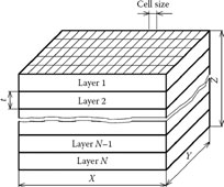
FIGURE 5.1
Multilayer component structure in the Microwave Office package.
Modules Voltaire LS and Voltaire XL allow analysis of the basic electric circuits consisting of linear and nonlinear elements as well as calculation of frequency and time responses.
The Microwave Office package is adapted for simulation of flat structure components, so models of symmetric or asymmetric meander delay systems can be easily designed because, in this case, it is enough to use one or two conductor layers between dielectric layers. The package does not allow simulation of helical systems with a circular cross section. Helical electrodes with elongated rectangular cross sections can be simulated by the system of two conductor layers. One conductor layer of such a system is shown in Figure 5.2. The lower layer conductors are not seen in the view of the upper layer. They are shown by dotted lines. Conductors of upper and lower layers can be interconnected with short-circuiters to model a helix.
According to the method of moments, the helix must be partitioned into finite elements. The initial partitioning is automatically performed by the package. Depending on the structure complexity, each initial element can be further partitioned into N elements. By default, Nmax = 100. It is important that finite elements simulating adjacent conductors not overlap.
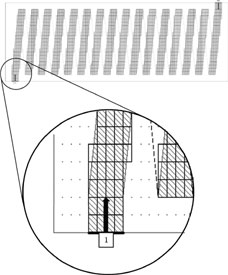
FIGURE 5.2
One-layer conductors in the model of a rectangular helix, their partitioning into finite elements, and a port of the helix.

FIGURE 5.3
The model of the simple helical system meeting Microwave Office requirements and developed using its internal graphical editor. 1: Helix conductor; 2: external shield; 3: short-circuiter.
Dimensions of the simulated structure and the number of finite elements determine the required computer random-access memory (RAM) and the computation time. If the computer RAM is insufficient, the number of finite elements should be reduced.
The model of the simple helical slow-wave system developed using the Microwave Office internal graphical editor is presented in Figure 5.3. The model consists of metal and dielectric layers, so it corresponds to the multilayer structure used in Microwave Office. The helix is installed in the external shield, which is at the distance c2 from the upper plane of the helix and at the distance q from the lower plane. The external and internal regions of the helix can be filled by dielectric with relative dielectric permittivity εr ≥ 1. In Figure 5.3, lL is the helix length, h is its width, L is the turn step, and l is the gap between the helical conductors.
Generally, the metal shield can also be installed inside the helix. Each turn of the helix or its part can differ in conductor width and thickness. In addition to ideal conductors, the model can contain conductors with limited conductivity. For this purpose, the following dimensions should be indicated: the conducting layer thickness p, the specific electric conductivity σ, and frequency f. In the low-frequency range, losses are evaluated by the surface square resistance
(5.1) |
In the high-frequency region, where the current skin depth is small (with respect to the thickness t of the conductor), losses are evaluated by the loss coefficient
(5.2) |
At skin depth close to the conductor thickness, both these factors are evaluated.
Turn parts of the helix in the vertical planes are not evaluated using Microwave Office; they are replaced by short circuiters.
5.1.1 Calculation of Amplitude and Phase-Frequency Responses of a Helical Slow-Wave System
When the helical system model is developed, it becomes a component (in this case, quadripole), the characteristics of which can be investigated using the program modules Voltaire LS and Voltaire XL. The block diagram of the system in the Microwave Office package medium and the signal path containing the system are presented in Figure 5.4(a, b).
Using the models shown in Figure 5.4, the amplitude-frequency and phase-frequency responses of a helical slow-wave system can be calculated directly. In the calculation, it is admitted that the signal source internal resistance ZG and the load resistance ZL are equal to the characteristic impedance ZC LF of the investigated helical system in the low-frequency range. The calculation results are presented in Figure 5.5(a, b).
Amplitude-frequency responses (Figure 5.5a) have an oscillating character that is caused by reflections. Reflections increase with frequency as a result of decreasing characteristic impedance of the helical system.
The distance between neighboring amplitude-frequency maximums or minimums is inversely proportional to the doubled delay time in the helical system. Losses in copper have only a small influence on the amplitude-frequency response. The phase-frequency characteristic of the system slightly differs from a straight line.

FIGURE 5.4
(a) The block diagram of the slow-wave system and (b) the signal path containing the system. EG: signal source; ZG: signal source internal resistance; ZL: load resistance.
Using the Microwave Office package, it was not possible to calculate the transient response of the system directly because the number of harmonics that can be taken into account is limited and it is impossible to model a unit step of voltage. However, transient response can be found at known amplitude and phase-frequency responses using
(5.3) |
where N is the number of frequency values, and Δω is the frequency variation step.
The transient response corresponding to frequency characteristics (Figure 5.5) obtained using Equation (5.3) is presented in Figure 5.6.

FIGURE 5.5
(a) Amplitude and (b) phase-frequency characteristics of the helical system obtained with ideal conductors (solid curves) and with evaluation of losses (dashed curves) at ZG = ZL = 160 Ω, ZCLF = 160 Ω, lL =17,b = 3,h = 10,L = 2,l = 1, c2 = 3, c1 = 0.4; helix conductor material: copper, thickness p = 0.2 mm.

FIGURE 5.6
Transient response of the helical system without losses.
Calculations of the transient response show that the pulse appears at the line output after the time equal to the line delay time. The rise time tr of the transient response is approximately 0.11 ns.
At the known rise time tr, the width of the equivalent pass-band of the system can be found:
(5.4) |
According to Figure 5.6, the width of the equivalent pass-band ΔFe of the considered helical system is 3.18 GHz. According to the amplitude-frequency response presented in Figure 5.5, the pass-band determined at the 0.707 level is wider (up to 3.5 GHz) because phase-frequency distortions are not taken into account.
5.1.2 Calculation of Phase Delay Time and Characteristic Impedance
It was further necessary to find a way that allowed evaluating the phase delay time and characteristic impedance of a slow-wave structure. The π-points and resonance methods were developed for measurement of phase delay time [1]. At short-circuited ends, a slow-wave system becomes a resonant system. At known resonant frequencies, the phase delay time versus frequency can be found using the relationship
(5.5) |
where fr is the resonant frequency, and n is the resonance order number.
Microwave Office allows modeling of the system short-circuited at its end and calculation of its scattering matrix parameter S21. Characteristic S21(f) is the transfer function of the system.

FIGURE 5.7
Parameter S21 of the helical system versus frequency at ZG = ZL ≈ 0 (lL = 33, c2 = 3, b = 3, c1 = 0.4, L = 2, l = 1, h = 10 mm).
The dependence of the parameter S21 on frequency, when the helix ends are short-circuited with shields, is presented in Figure 5.7. The resonant frequencies can be determined by Microwave Office internal graphical analysis facilities, and the delay time at the resonance frequency can be found using Equation (5.5).
At known phase delay time, the retardation factor is given by
(5.6) |
where lL is the helix length.
The phase delay time versus frequency calculated using characteristic S2l(f) and Equation (5.5) is represented by curve 1 in Figure 5.8.
The phase delay time can also be found at known phase-frequency characteristic φ(ω):
(5.7) |
where vph is the phase velocity of the electromagnetic wave propagation along the helix.
The phase delay time frequency characteristic computed using the phase-frequency characteristic (Figure 5.5b) is represented by curve 2 in Figure 5.8. According to this figure, phase delay time frequency characteristics, obtained using considered methods, practically coincide.
Reflections in the signal path with a slow-wave system (Figure 5.4b) do not exist if the internal resistance of the signal source and load resistance are the same as the characteristic impedance of the slow-wave system (at ZG = ZC = ZL). Therefore, at a selected frequency, the system characteristic impedance can be determined by changing the signal source and load resistances (ZG = ZL) until minimal reflections are obtained. Then, ZC ≅ ZG = ZL. The graph of helical system characteristic impedance versus frequency obtained on the basis of the described idea is presented in Figure 5.9. Characteristic impedance decreases with frequency.

FIGURE 5.8
Frequency dependences of the delay time calculated using different methods. 1: Using Equation (5.5); 2: Using Equation (5.7).
The character of the graph (Figure 5.9) corresponds to known results [1,2]. On the other hand, errors appear in the calculation of characteristic impedance because of reactivities at the ends of the system. We can send the probe signal to the middle of the slow-wave system (Figure 5.10) in order to reduce influence of these reactivities.
According to Figure 5.10, the slow-wave system is loaded by resistances that are equal to characteristic impedance of the system. Internal reflections from port 3 (Figure 5.10a) are minimal if the internal resistance of the probe signal source is equal to half of the characteristic impedance of the slow-wave structure or if it is infinitely great (in practice, considerably greater than the characteristic impedance of the system that is under investigation). According to calculations, results Z′G = ZL/2 coincide with results at Z′G = 10 kΩ. It is important that, using circuits presented in Figure 5.10, we are able to find variation of characteristic impedance along the slow-wave system.
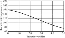
FIGURE 5.9
Characteristic impedance versus frequency of the helical system (Figure 5.3) found at condition ZG = ZC = ZL.

FIGURE 5.10
(a) Model of a helical slow-wave system and (b) signal path developed for calculation of characteristic impedance of the system.
Application of the Microwave Office package shows that models of complex shielded helical systems, which practically do not differ from the real simulated objects (their design drawings), can be developed using the EMSight module. The phase delay time and characteristic impedance frequency characteristics of the helical slow-wave system obtained using Microwave Office coincide with those obtained using the electrodynamic and multiconductor line methods and presented in published papers and monographs [1,2] and Chapters 1 and 4.
For the quantitative comparison of investigation results, dependences of the delay time and the characteristic impedance on frequency in the case of the helix asymmetrically mounted inside the external shield are presented in Figure 5.11(a, b). Characteristics obtained using Microwave Office are shown by the solid line, and characteristics obtained using the multiconductor line method are presented by dashed lines. According to Figure 5.11(a), the retardation coefficient calculation results differ by not more than 8–10% and characteristic impedance results up to 30%.
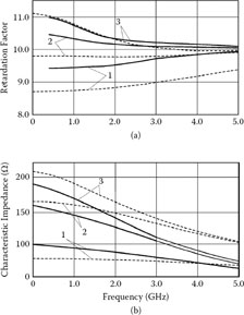
FIGURE 5.11
(a) Retardation factor of helical system and (b) its characteristic impedance versus frequency at lL = 25, b = 3, h = 10, c1 = 0.4, L = 2, l = 1, p = 0.25. 1: c2 = 0.4; 2: c2 = 3; 3: c2 = 9 mm (solid lines: characteristics obtained using Microwave Office when conductor material—copper, dashed lines—characteristics obtained using the multiconductor line method).
Relatively great differences in values of characteristic impedance are related to the analytical method used for calculation of characteristic impedances of multiconductor lines in the model of the helical structure. This method did not allow simulating of thin conductors. In spite of this, the characters of dependences in the investigated range coincide. Calculations using the Microwave Office package completely confirmed results, obtained with an analysis of a helix asymmetrically mounted inside the external shield, using the electrodynamic method and presented in Section 1.3 in Chapter 1.
5.2 Investigation of the Twined Helical Slow-Wave System
A new version of the delay and deflection system, the twined helical system proposed in Correll and Ronald [9], is investigated by the multiconductor line method in Chapter 4. Properties of such complex delay systems are compared with properties of ordinary helical systems.
In this section, we will use the Microwave Office program package for investigation of the twined helical system in order to check possibilities of its application for investigation of complex helical systems and to compare the obtained results with those obtained using the multiconductor line method [7,8,16]. To this end, models of the twined helical system containing conductors with constant and periodically varying width, as well as signal paths containing the twined system and investigation methods, have been developed.
5.2.1 Models of the Twined Helical System
A model of the twined helical system developed using the Microwave Office internal graphical editor is presented in Figure 5.12. The model consists of layers of conductors and dielectrics so that it corresponds to the multilayer structure used in Microwave Office. In the model, the twined helices are inserted into an external shield, which is at the distance c2 from the upper plane of helices and at the distance c1 from the lower plane. The helix turn parts, the height of which is b, that are in the vertical planes are not evaluated. The helix width h, height b, and the step L determine the value of the structural retardation kRs.

FIGURE 5.12
Model of the twined helical system meeting the requirements of Microwave Office. 1 and 2: Helical electrodes; 3: shield; 4: short-circuiter.

FIGURE 5.13
The circuit containing the twined helical system (THS) at asymmetrical feeding.
Let us assume that in Figure 5.12, h = 10 mm, L = 5 mm, the width of narrow turn elements ln = 1 mm and that of wide turn elements lw = 2 mm, and kRs = 4. Dielectric layers are described as vacuums. The helical system is analyzed in the restricted rectangular multilayer volume. Lateral, upper, and lower limits of this volume are of an ideal conductor.
Initially, let us consider circuits containing twined systems with constant widths of helical conductors (ln = lw = l mm) and step L = 5 mm.
According to the circuit diagram presented in Figure 5.13, one helix of the twined system is used as active, and the other helix is passive. The signal source is connected to input 2 of the active helix. Electromotive force of the signal source is EG, and its internal resistance is ZG. The load resistance of the active helix is ZL; the passive helix is loaded with ZL1.
The amplitude-frequency responses of the circuit (Figure 5.13) at ZL1 = 1 Ω (in fact, when the terminals of the passive helix are short-circuited to the shield) are presented in Figure 5.14. The solid line characterizes transfer of the input voltage to the output of the active helix, and the dashed line shows transfer to the output of the passive helix. According to this figure, the transfer of the voltage in the circuit greatly depends on the loads of the passive helix. Signal propagating along the active helix induces the electromotive force in the passive helix. At indicated conditions, the passive helix operates as a resonator. Due to coupling of helices, the amplitude-frequency characteristic of the active helix falls to low levels at resonant frequencies of the passive helix. We can use characteristics presented in Figure 5.13 for calculation of phase delay time in the twined helical system.
The amplitude-frequency response of the active helix at asymmetrical feeding and matched loads of twined helices is presented in Figure 5.15.

FIGURE 5.14
Amplitude-frequency responses of the twined helical system at asymmetrical feeding, constant widths of helical conductors, and passive helix load resistances of 1 Ω. 1: Characteristic illustrating transfer to the output of the active helix; 2: transfer to the output of the passive helix.
In this case, variation of the characteristic is considerably less because incident waves are absorbed in the loads. On the other hand, it is important that losses in the passive helix cause additional fall of amplitude-frequency characteristics of the active helix with increase of frequency.
With application of the twined helical system in a traveling-wave cathode-ray tube, signals from outputs of the paraphase amplifier are sent to the system for deflecting of the electron beam. This mode of operation can be modeled by the circuit diagram presented in Figure 5.16. The phase shifter Φ is used in the circuit. Then, the characteristic impedance of the system depends on phase difference φ between voltages sent to inputs of helices. At φ = π, the odd mode, and at φ = 0, the even wave, are excited in the system. Characteristic impedances of the system for even and odd waves are different (ZCe and ZCo). Thus, load resistances necessary for matching depend on the type of electromagnetic wave in the system and, of course, on frequency.

FIGURE 5.15
Amplitude-frequency response of the active helix of the twined helical system at asymmetrical feeding, constant widths of helical conductors, and helices loaded with ZL = LL1 = ZG = ZC = 130 Ω.

FIGURE 5.16
The circuit modeling the twined helical system at even- and odd-operation modes.
The principles and methods just described were used for finding phase delay time and characteristic impedance frequency characteristics.
Phase delay time and characteristic impedance versus frequency at even and odd waves in the system are presented in Figure 5.17. According to Figure 5.17(a), the phase delay time of the odd mode in the twined helical system is almost constant in the wide-frequency range. Dispersion of the phase delay time of the even wave is also small (less than 0.05 ns in the frequency range to 10 GHz).

FIGURE 5.17
(a) Phase delay times and (b) characteristic impedances of the twined helical system versus frequency at odd (curves 1) and even (curves 2) waves when lL = 33,b = 3,L = 5,ln = lw = l,h = 10, C1 = 1, c2 = 1 mm, and helix conductor thickness p = 0.2 mm (material: copper).
Characteristic impedance of an ordinary helical system decreases with frequency. The characteristic impedance of the twined helical system in the case of the even mode also slightly decreases with frequency. The characteristic impedance at propagation of the odd mode increases with frequency. This effect is explained in Chapter 4 for analysis of the twined helical system using the multiconductor line method. An increase of the impedance is related to a decrease of the phase angle between voltages on adjacent helical conductors with frequency and a decrease of the distributed capacitances of helices.
Calculated amplitude-frequency responses of the twined helical system at even and odd modes of operation are presented in Figure 5.18. In the calculations, load resistances are selected equal to corresponding characteristic impedances in the low-frequency range. As the same signal source is used for feeding of helices, its internal resistance equals half the load resistance (ZG = ZL/2). Losses in the helices are taken into account using Equations (5.1) and (5.2). Because the system consists of two symmetrical parts, their frequency responses are identical.
According to Figure 5.18, ripples of amplitude-frequency characteristics appear when the frequency becomes higher than 2 GHz. They are caused by variation of characteristic impedances with frequency and multiple reflections from the input and output of the system. The distance between frequency values corresponding to neighboring minimums or maximums of the amplitude response is inversely proportional to the phase delay time.
According to simulation, the width of the pass-band at propagation of even and odd waves is more than 10 GHz if the retardation factor is small (kR ≅ 5) and gaps between neighboring helical conductors are 1.5 times greater than the conductor width.

FIGURE 5.18
The amplitude-frequency responses of the twined helical system when ln = lw = const. 1: At odd mode (φ = π), ZG = 52 Ω, ZL = ZCo = 104 Ω; 2: at even mode (φ = 0°), ZG = 75 Ω, ZL = ZCe = 150 Ω.
5.2.2 Properties of the Twined System at Varying Widths of Helical Conductors
In twined helical traveling-wave deflection systems, widths of helical conductors periodically change along the system (Figure 5.12). A turn of a helix consists of two parts: wide and narrow. Thus, lw > ln.
The amplitude-frequency response of the twined helical system at varying widths of conductors is presented in Figure 5.19. In order to accelerate calculations, losses in the system are not taken into account. Curves 1 and 2 are obtained for odd and even waves in the system, respectively.
Comparison of characteristics in Figures 5.18 and 5.19 shows that periodical variation of widths of helical conductors causes nonuniformities of transfer responses. As a result, the stop-bands appear in the frequency range of 6–8 GHz. (This property of the system is discussed in Chapter 4.) The non-uniformities of the responses are the consequence of multiple reflections and resonances in the system containing periodical inhomogeneities. The central frequencies of the stop-bands are dependent on the period of inhomogeneities and can be estimated using the formula
(5.8) |
where 2(h + b) is the period of inhomogeneities along the helical conductor, and ratio 2(h + b)/c0 defines the approximate value of the phase delay time in the period.
The exact value of the central frequency can be found using information about phase delay time or retardation factor. According to Figure 5.19, the central frequency of the stop-band at the even mode is slightly higher because the phase delay at this mode is less than the phase delay at the odd wave (Figure 5.17a).
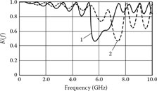
FIGURE 5.19
The amplitude-frequency responses of the twined helical system at periodical variation of widths of helical conductors (lw/ln = 1.5). 1: At odd mode (φ = π), ZG = 48 Ω, ZL = ZCo = 96 Ω; 2: at even mode (φ = 0°), ZG = 71 Ω, ZL = ZCe = 142 Ω.

FIGURE 5.20
The amplitude-frequency responses of the twined helical system at periodical variation of widths of helical conductors (lw/ln = 2). 1: At odd mode (φ = π), ZG = 42 Ω, ZL = ZCo = 84 Ω 2: at even mode (φ = 0°), ZG = 69 Ω, ZL = ZCe = 138 Ω.
The width of the stop-band depends on inhomogeneities. The amplitude-frequency responses of the twined helical system at an increased ratio of widths of helical conductors are presented in Figure 5.20. Comparison of the responses in Figures 5.19 and 5.20 shows that an increase of periodical inhomogeneities is followed by an increase of the width of the stop-band. Thus, periodical inhomogeneities in the twined helical traveling-wave deflecting system cause nonuniformity of the amplitude-frequency response and limit the width of the pass-band of the system.
Results of simulation using the Microwave Office package coincide with properties of the twined helical system discovered using the multiconductor line method (presented in Section 4.1 in Chapter 4).
5.3 Input Impedance of Helical Systems
Due to scattering of the electric field at the ends of slow-wave structures with limited length, capacitive reactivities appear [2]. The magnitudes of such reactivities depend on the type of structure, its design, characteristic impedance, etc. Various methods have been developed for improvement of characteristics of signal paths containing slow-wave structures with limited length. In devices with pass-band to 1 GHz, inductive elements in series with slow-wave structures can be used for compensation of increased capacitances at the input and output of the structures [2]. In devices with wider pass-band, narrowed conductors are used at the ends of slow-wave systems [2,12]. At the same time, questions related to compensation and reduction of end reactivities of slow-wave structures remain problematic.

FIGURE 5.21
The model of an ordinary helical slow-wave system composed using the internal graphical editor of the Microwave Office program package. 1: Helix; 2: external shield; 3: end turn of the helix.
Taking this into account, we used the Microwave Office package for investigation of input and characteristic impedances of an ordinary helical system and possibilities to reduce end reactivities. Results published in Skudutis and Daskevicius [10,11] are generalized in this section.
The model of an ordinary helical slow-wave system composed using the internal graphical editor of the Microwave Office program package is presented in Figure 5.21. The system consists of a helix with rectangular cross section and external shield. Let us assume that the space inside the shield is vacuumed. Then, the characteristic impedance of the system depends on the cross-section dimensions of the helical conductor, step, cross-section dimensions of helix, and distance of the shield from the helix. It is known that a change of characteristic impedance with frequency and the influence of end reactivities of a helix are greater at higher characteristic impedances [2]. For this reason, we considered the system at dimensions (h = 10, L = 2,l = 1, b = 2, c1 = c2 = 1 mm) that let us obtain relatively high characteristic impedance (close to 150 Ω).
In order to reveal the influence of the end turns of the helix on frequency properties of the helical system, in addition to the basic model presented in Figure 5.21, we composed and considered additional models with different design of the end turns (Figure 5.22).
The results of calculations and their analysis [10,11,14,15] allow discovering the essence of processes in the signal paths containing slow-wave structures with limited lengths and finding better methods for matching in the high-frequency range. The end turns of helices must be considered as the sections of lines and can play roles of matching impedance transformers.
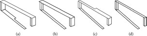
FIGURE 5.22
Views of the end turn of the helix in the helical system (Figure 5.21).
The calculation results of input impedances of helical systems at various designs of end turns (Figures 5.21 and 5.22) are presented in Figure 5.23. According to this figure, at a constant width of helical conductor (Figure 5.21), the input impedance of the helical system decreases with frequency (curve 1 in Figure 5.23). At the frequency when the length of turn is equal to half the wavelength, the input impedance becomes minimal, about 30% less than that in the low-frequency range.
The narrowed end turn operates as an impedance transformer. At frequency
(5.9) |
it becomes a quarter-wave length impedance transformer, and the input resistance of the helical system becomes maximal.
Curve 2 (Figure 5.23) satisfies that the matching section is too long, its width is too small, and the characteristic impedance is too high for matching of the signal path in the wide-frequency range.

FIGURE 5.23
Input impedance of the helical system versus frequency at various designs of end turns. 1: Width of helical conductor is constant; 2: the end turn is narrowed to 50%; 3: the initial part (one-half) of the end turn is narrowed to 50%; 4: the initial part (one-fourth) of the end turn is narrowed to 50%.
The frequency at which the input impedance becomes maximal increases with a decrease of the matching section (narrowed part of the end turn) length.
The optimal characteristic impedance Zct of the quarter-wave length impedance transformer depends on nominal characteristic impedance Zn of the signal path and characteristic impedance Zc(f) of the system: . Thus, characteristic impedance ZCt is dependent on frequency. As the characteristic impedance of the helical system decreases with frequency, the matching section with higher characteristic impedance is necessary for matching at higher frequencies (curves 3 and 4). As a result, minimal variation of the input impedance of the considered helical system at the end turn narrowed to 50% is obtained when the length of the narrowed turn is equal to one-fourth of the turn length; the section of the narrowed turn operates as a quarter wave length impedance transformer at high frequency (curve 4 in Figure 5.23).
Amplitude-frequency responses of the signal path containing the helical system are shown in Figure 5.24. The curves were obtained at the same conditions as input impedance characteristics in Figure 5.23. The responses illustrate that frequency properties of the signal path depend considerably on using matching elements. Multiple reflections from the output and input of the system cause oscillations of the responses. The distance between neighboring minimums or maximums depends on the phase delay time in the helical system and is given by
(5.10) |
Amplitude-frequency responses (Figure 5.24) confirm the effectiveness of the application of matching sections of end turns of the helix. Nonuniformity of the amplitude-frequency response in the wide frequency range is minimal in the design of the end turns presented in Figure 5.22(a) and there is minimal variation of the input impedance (curve 4 in Figure 5.23).
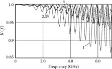
FIGURE 5.24
Frequency responses of the signal path containing the helical slow-wave system at various designs of end turns. 1: Width of helical conductor is constant; 3: the initial part (one-half) of the end turn is narrowed to 50%; 4: the initial part (one-fourth) of the end turn is narrowed to 50%.

FIGURE 5.25
Input impedance of the helical system versus frequency at various designs of end turns. 1: Width of helical conductor is constant; 2: the end turn is narrowed to 75%; 3: the initial part (three-fourths) of the end turn is narrowed to 75%; 4: the initial part (one-half) of the end turn is narrowed to 75%.
It was noticed that the characteristic impedance of the end turn narrowed to 50% was too high for the considered helical system. Additional calculations performed in the case of the end turns narrowed by 25% confirmed this idea. Graphs of the input impedance of the helical system versus frequency and amplitude-frequency responses of the signal path at end turns narrowed by 25% are presented in Figures 5.25 and 5.26. Analysis of characteristics (Figures 5.23,5.24,5.255.26) shows that the initial parts of the end turns narrowed by 25% really allowed achieving better matching of the signal path.
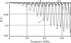
FIGURE 5.26
Frequency responses of the signal path containing the helical slow-wave system at various designs of end turns. 1: Width of helical conductor is constant; 3: the initial part (three-fourths) of the end turn is narrowed to 75%; 4: the initial part (one-half) of the end turn is narrowed to 75%.
Nonuniformity (ripples) of the amplitude response in the frequency range to 5 GHz is minimal at the narrowed three-fourths of the end turn length. Ripples in the wider a smaller range are less at a smaller less length of the matching section.
Generally, conditions of the optimal matching of the signal path are dependent on nominal characteristics of the signal path, design of the slow-wave structure, and other factors. At the same time, it is important that versatile software packages like Microwave Office allow solving problems related to matching of signal paths containing slow-wave structures and improvement of frequency properties of the signal paths.
Specific problems related to matching of signal paths in traveling-wave cathode ray tubes, frequency, and transient responses of traveling-wave deflecting systems and traveling-wave cathode-ray tubes are considered in Chapter 7.
5.4 Resonances in the System of Shields and Possibilities of Avoiding Them
Helical systems containing internal and external shields are qualified as prospective and are applied in super-wide-band traveling-wave devices [2]. On the other hand, at limited length, the shields of the system form a line that is short circuited at its ends. As a result, the system of the shields can operate as a resonator and influence properties of the helical system and electronic device [19].
Nonuniformities of frequency characteristics caused by resonances in the system of the shields have been detected at measurements of standing-wave coefficients in the signal path containing the helical system with internal and external shields [2]. Results of investigations performed in order to reduce the influence of resonances in the system of the shields are presented in Vainoris, Gerasimavicius, and Staras [13] and Maceika and Malisauskas [14]. According to the latter, we can avoid resonant effects when the odd number of the halves of the slow-wave fit along the length of the helix of the system. Vainoris et al. [13] state that resonances do not exist when an integer number of half-waves fit along the helix.
In this section, we generalize the results of research of resonant effects in the helical system using the Microwave Office package in order to reveal conditions at which resonant effects exist and how to avoid these effects [15,16,17,18].
5.4.1 Model and Methodology of Investigation of the System
The model of the helical system containing internal and external shields composed using the internal graphical editor of the Microwave Office software package is presented in Figure 5.27. The system consists of helix 1, internal shield 2, and external shield 3. Helix width h, its height b, and step L determine the structural retardation of the system. At selected dimensions of the helix, the necessary characteristic impedance can be achieved, changing the gaps between the helix and its shields.
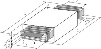
FIGURE 5.27
Model of the helical system containing internal and external shields composed using Microwave Office. 1: Helix; 2: internal shield; 3: external shield.
We investigated the described helical system at helix width h = 10 mm, height b = 2.4 mm, step L = 2 mm, width of the helical conductor lc = 1 mm, width of the internal shield d1 = 7 mm, gaps between the helix and the shield a1 = a2 = 1.2 mm, and gaps between the helix and the external shield c1 = c2 = 1.5 mm. At specified dimensions, the characteristic impedance of the system in the low-frequency range according to calculations was 150 Ω. In order to improve the matching of the system with the signal path, the end turns of the helix were designed according to results presented in Section 5.3.
The diagram of the circuit used for investigation of the helical system is presented in Figure 5.28, where EG is electromotive force of the signal source, ZG is its input resistance, and ZL is the load resistance of the helical system.
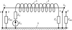
FIGURE 5.28
Diagram of the circuit for investigation of the helical system containing internal and external shields. 1: Helix; 2: internal shield; 3: external shield.
Switches S1 and S2 allow short-circuiting of the shields at their ends and loading the line formed by the shields with load resistances Zsh1 and Zsh2.
We considered amplitude-frequency, phase-frequency responses of the helical system, and its input impedance and delay time versus frequency, analyzing effects caused by resonant properties of the system of the shields. In order to simplify modeling and calculations, we did not take into account losses in the elements of the system. The phase delay time was determined using the phase-frequency response φ(ω) of the system and Equation (5.7).
5.4.2 Application of Microwave Office for Investigation of Resonant Effects
Amplitude-frequency responses of a helical system at helix length Ls = 33 mm and length of shields Lsh = 34 mm are presented in Figure 5.29. The ″1″ curves were obtained at short-circuited shields at their ends and the ″2″ curves at shields short-circuited at one end and loaded with Zsh2 = 100 kΩ (at position 2′ of switch S2). According to Figure 5.29, great nonuniformities of amplitude-frequency responses are evident in both specified cases.
In the case when the shields are short-circuited at both ends, nonuniformities of amplitude-frequency response in the frequency range to 10 GHz are seen at frequencies frl = 4.2 GHz and fr2 = 8.4 GHz. Assuming that the space is vacuumed and the propagation velocity of the wave in the line consisting of the shields is c0, using formula
(5.11) |
we can find that wavelengths λrl = 71 mm and λr2 = 35.5 mm correspond to frequencies frl and fr2. Thus, uniformities of the amplitude response appear at Lsh ≅ λrl/2 and at Lsh ≅ λr (i.e., when an integer number of half-waves fit along the system of the shields).
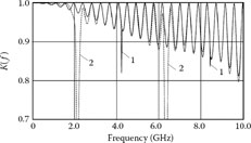
FIGURE 5.29
Amplitude-frequency responses of the helical system with shields short-circuited at both ends (curve 1) and short-circuited at one end (curve 2).
Similarly, we can easily find that in the case when shields are short-circuited at one end, inhomogeneities of the amplitude-frequency response exist when odd number or wave quarters fit along the shields.
Presented results of calculations satisfy that the Microwave Office program package allows determining resonances in the system of the shields and can be used for further investigations in order to examine possibilities to avoid the bad influence of resonant effects on properties of helical systems.
Usually, in practice, shields short-circuited at both ends are used. Then resonances in the system of the shields and nonuniformities of frequency responses of the helical systems are possible at frequencies
(5.12) |
where n = 1,2,3,…
According to Equation (5.12), at length of the shields Lsh ≤ 60 mm, only one resonance is possible in the frequency range to 8 GHz.
5.4.3 Possibilities for Avoiding Resonant Effects
In order to reveal conditions at which resonant effects can be avoided, we examined amplitude-frequency responses of the helical systems and their delay time frequency characteristics in the frequency range to 10 GHz at a helix length of 33 mm and various lengths of the shields. Calculated characteristics are presented in Figures 5.30 and 5.31.
At the length of the internal shield Lsh = 27 mm, only one resonance in the specified frequency range is possible at fr = 5.3 GHz when half of the wavelength fits along the system of short-circuited shields (curve 1 in Figure 5.30). At Lsh = 38 mm, two resonances (curve 2) appear at frequencies corresponding to n = 1 and n = 2, according to Equation (5.12).

FIGURE 5.30
Amplitude-frequency responses of the helical system containing short-circuited shields at various lengths of the internal shield: 1: Lsh = 27; 2: Lsh = 38; 3: Lsh = 33 mm.
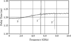
FIGURE 5.31
Phase delay time in the helical system versus frequency at various lengths of the internal shield. 1: Lsh = 27; 2: Lsh = 38; 3: Lsh = 33 mm.
The wave propagating along the helical system does not excite resonances (Figure 5.30, curve 1) when the length of the shields is the same as the length of the helix.
Phase delay time frequency characteristics of the examined systems practically coincide except for narrow frequency ranges near resonant frequencies (Figure 5.31).
According to presented characteristics and other results of calculations, it is possible to avoid resonances when the length of the shields is the same as the length of the helix and the helix contains an odd number of turns. Under these conditions, the situation at both ends of the helical system is identical, and resonances are not excited.
In order to determine the influence of reactivities at the ends of the helical system on the characteristics of the system, we composed the model (Figure 5.32) containing the internal shield shifted along the system by one step of the helix. The length of the shield was the same as the length of the helix. At these conditions, the amplitude-frequency response of the helical system contained inhomoheneities. At switches S1 and S2 used in positions 2 and 2′ (Figure 5.28) and loads Zshl = Zsh2 = 1 Ω, relatively high voltage drops appeared even on small load resistances connecting the ends of the shields (Figure 5.33).
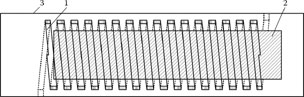
FIGURE 5.32
The helical system containing an internal shield shifted along the longitudinal axis. 1: Helix; 2: internal shield; 3: external shield.

FIGURE 5.33
Frequency characteristic showing transmission of the signal from the helix to the system of the internal and external shields.
Thus, different reactivities at the ends of the helical system complicate avoidance of resonant effects in the system.
A helical system containing a helix and shields of the same length cannot be realized. In practice, the lengths of the shields are greater than the length of the helix. This circumstance is taken into account in Vainoris et al. [13] and Maceika and Malisauskas [14].
In order to reveal conditions at which resonant effects can be avoided with lengthened shields, the internal shield having the form of the meander was used in the model (Figure 5.34). Calculated frequency characteristics of such a system are presented in Figures 5.35 and 5.36.

FIGURE 5.34
Helical system containing an internal shield in a form of a meander. 1: Helix; 2: internal shield; 3: external shield.
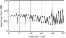
FIGURE 5.35
Input impedance of the helical system containing an internal meander-like shield versus frequency.
Figure 5.35 illustrates the influence of resonances in the system of the shields on input impedance of the helical system. Caused by resonances, variation of input impedance is not seen in the frequency range from 4.5 to 7 GHz; oscillations induced into the system of the shields are small, in the frequency range from 5.3 to 6.3 GHz. According to calculations, at the first resonant frequency in the last frequency range, four half-waves fit along the internal shield and seven half-waves fit along the helix. At higher frequencies, five half-waves fit along the shields, and eight half-waves fit along the helix.
Thus, the conclusion made by Vainoris et al. [13] regarding conditions that led to avoiding resonant effects in the helical system containing internal and external shields is right: It is possible to avoid the influence of the resonant system formed by the shields on properties of the helical system if an integer number of delayed half-waves fit along the helical system. On the other hand, then only one resonant frequency is possible in the pass-band of the helical system, and thus Maceika and Malisauskas [14] are also right: It is possible to avoid resonance if the odd number of half-waves fit along the helical system.

FIGURE 5.36
Frequency characteristic showing transmission of the signal from the helix to the system of the internal and external shields with a meander-like form of the internal shield.
Thus, we can avoid expensive experimental work in the design of slow-wave structures and, using versatile software for investigation of electromagnetic fields and design of microwave devices (such as Microwave Office), detect the influence of resonant phenomena in systems of elements of slow-wave structures and find optimal technical decisions.
5.5 Application of Software for Three-Dimensional Modeling
Application of the Microwave Office package offered advantages of numerical methods and modern software for investigation of electromagnetic fields and design of microwave objects. On the other hand, the version of the Microwave Office software package used has been developed for planar two-dimensional (2D) object modeling. Using Microwave Office, difficulties arise at modeling of lateral parts of helices with elongated rectangular cross sections, short-circuiters of shields, dielectric holders in slow-wave structures, and other elements of the structures. Also, Microwave Office requires relatively great hardware resources.
New opportunities for research of slow-wave structures appear with the application of software developed for three-dimensional (3D) modeling. In this section, we generalize the experience obtained from application of the software system MicroWave Studio (MWS) developed by the German company Computer Simulation Technology (CST) for three-dimensional electromagnetic simulation of high-frequency components. We used the MicroWave Studio tools for the simulation of wide-band slow-wave systems [21,25,28].
5.5.1 Brief Information about MicroWave Studio Tools
The MicroWave Studio software system [20] enables the fast and accurate analysis of high-frequency devices. The system, based on the numerical finite integration method, contains a user-friendly interface, powerful model drawing tools, and fast solvers. In addition to the flagship module, the broadly applicable time domain solver and the frequency domain solver, the CST MWS offers additional solver modules for specific applications and uses innovations such as perfect boundary approximation (PBA), the thin sheet technique (TST), the multilevel subgridding scheme (MSS), etc.
The frequency domain solver can be switched from Cartesian to tetrahedral meshing for better representation of curved surfaces. The perfect boundary approximation uses proprietary techniques for geometry generation and modeling of curved surfaces (Figure 5.37a). The thin sheet technique extends the capabilities of perfect boundary approximation by enabling the independent treatment of two dielectric parts of a cell, separated by a metallic sheet. Structures such as arbitrarily shaped housings or thin inclined shields can be modeled with a minimum of effort. CST MWS version 5 introduced the multilevel subgridding scheme that allows mesh lines to start and be terminated anywhere in the simulation area and to use increasingly finer mesh (Figure 5.37b).

FIGURE 5.37
Example of a splitting grid of coaxial line by method PBA (a) and by method MSS (b).
The key application for the frequency domain solver is periodic structures. Floquet-mode solvers were developed for highly accurate and fast simulation. The transient solver also delivers broadband frequency domain results like S parameters. These simulations can be performed with an arbitrary fine frequency resolution without extra computational cost, thus avoiding missing single resonances inside the spectrum. Field results for many frequencies can be derived from one single simulation run.
Calculated S parameters can be represented in the form of graphs or tables or saved using the special touchstone format. Additionally, the MWS allows composition of the equivalent circuit of the considered object in SPICE format.
Wide-band helical and meander slow-wave systems can be qualified as specialized electromagnetic devices. For this reason, let us consider the possibilities of the application of the CST MWS tools for simulation of helical and meander systems.
In order to check the suitability of the MWS software for simulation of helical systems, let us consider the helical system containing an anisotropic shield. Anisotropic shields are widely used in helical delay lines [1]. Sometimes, they are also used in traveling-wave deflecting systems for correction of dispersion characteristics [2].
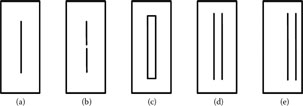
FIGURE 5.38
Cross-section views of helices containing various types of internal shields. (a) Isotropic shield inserted symmetrically with respect to the helix; (b) the shield with a longitudinal gap; (c) isotropic shield with increased cross section; (d) the shield in the form of two parallel plates; (e) the shield in the form of two parallel plates displaced asymmetrically with respect to the helix.
Views of cross sections of helices with various types of internal shields are presented in Figure 5.38. The dimensions of the basic types of systems (Figure 5.38a) were selected to obtain characteristic impedance ~ 100 Ω and retardation factor ~ 12.5: Width of the helix h = 10 mm, its thickness b = 2.5 mm, step L = 2 mm, width of the helical conductor l = 1 mm, and length of the helix = 42 mm [21].
In the application of the MWS, the draft of the system is composed using the internal graphical editor, and input and output ports are specified. Methods developed in the application of the Microwave Office program package (Subsection 5.1.2) can be used for calculation of phase delay time and characteristic impedance.
Phase delay time frequency characteristics calculated for systems with cross sections presented in Figure 5.38(a, b) are presented in Figure 5.39.

FIGURE 5.39
Phase delay time versus frequency calculated at 1: Thin isotropic internal shield (Figure 5.38a); 2: the thin shield with the longitudinal gap (Figure 5.38b); and 3: the thin shield with two longitudinal gaps.

FIGURE 5.40
Phase delay time versus frequency calculated at 1: Solid internal shield (Figure 5.38c); 2: the shield in the form of two parallel plates (Figure 5.38d); and 3: the shield in the form of two parallel plates displaced asymmetrically with respect to the helix (Figure 5.38e).
According to this figure, longitudinal gaps made in the thin internal shield have only a small influence on dispersion properties of the helical system. The shields with longitudinal gaps can be qualified as anisotropic. According to Vainoris, Kirvaitis, and Staras [1], anisotropic shields cause an increase of distributed inductivity and an increase of the phase delay time in the low-frequency range. Curves 1 and 2 in Figure 5.39 indicate the opposite tendency: Making of a longitudinal gap is followed by a small decrease of the phase delay time. The increase of the phase delay time at very low frequencies becomes noticeable only at two longitudinal gaps (curve 3).
The graphs of the delay time frequency characteristic for the helical systems with cross sections shown in Figure 5.38(c, d, e) are presented in Figure 5.40. This figure shows that, at the isotropic internal shield (Figure 5.38c), the phase delay time of the helical system slightly increases with frequency (curve 1). The internal shield in the form of two parallel plates (Figure 5.38d) at the same cross-section dimensions as the isotropic shield causes an increase of the phase delay time with a decrease of frequency (curve 2). An additional increase of the phase delay time appears (curve 3) at the asymmetrically inserted shield (Figure 5.38e) due to periodical variation of characteristic impedance along the helical conductor [22].
5.5.3 Investigation of the Influence of Periodical Inhomogeneities
Periodical inhomogeneities are inherent for helical systems with rectangular cross sections. Dielectric holders of elements in helical systems cause additional periodic inhomogeneities. According to Staras and Burokas [22], the helical system with a periodical inhomogeneity along a helix turn obtains properties of the rejection filter when the phase angle θ between voltages on neighboring helical conductors approaches π. In order to improve frequency properties, we must decrease the period of inhomogeneities along the conductor.

FIGURE 5.41
(a) The cross-section view of the helical system and (b) its amplitude-frequency response.
The cross section of the helical system containing the dielectrical holder and its amplitude-frequency response are shown in Figure 5.41. According to the amplitude-frequency response, the system really obtains rejection properties.
Using the idea about the relationship between the central frequency of the stop-band and period of inhomogeneities, we easily found the way that allowed improving frequency properties of the helical system and widening its pass-band. The improved design of the helical system is presented in Figure 5.42(a). The system contains the dielectric holder for the helix and asymmetrically inserted internal shield. Because of two inhomogeneities and a lesser period of inhomogeneities along a helix turn, frequency properties of the system are considerably better (Figure 5.42b).
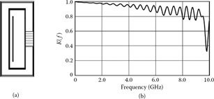
FIGURE 5.42
(a) The helical system containing a dielectric holder, asymmetrically inserted internal shield, and (b) the amplitude response of the system.

FIGURE 5.43
The amplitude-frequency response of the helical system.
With an increase of periodical inhomogeneities, the width of the stop-band increases. As an example, the amplitude-frequency response of the helical system containing the solid dielectric holder with high dielectric permittivity (εr = 9) is presented in Figure 5.43. Periodical inhomogeneities in the system are determined by parasitic capacitances between the helical conductor and the external shield, and parasitic capacitances between neighboring turns of the helix that increase with frequency because the phase angle between voltages of neighboring helical conductors increases with frequency. In order to reduce the last capacitances, dielectrical holders made of material with less dielectric permittivity or comb-type dielectrical holders are used [2]. For further reduction of capacitances between neighboring helical turns, we proposed using two-row comb-type dielectrical holders [23]. The model of the helical system with such holders composed using the internal graphical editor of the MWS package is presented in Figure 5.44. At increased distance between holding elements, parasitic capacitances are lower, and the width of the pass-band of the system is considerably greater (Figure 5.45).
The calculations performed revealed advantages of MicroWave Studio with respect to Microwave Office. The MWS program system allows simulation of three-dimensional structures, dielectrical holders, short-circuiters, and other elements of real systems. In calculation of S parameters, all elements of the composed model and effects in it (for example, reactivities at the ends of a system) are taken into account. At the same time, calculations are considerably faster.
Thus, the MWS program system can be efficiently applied for investigation and design of wide-band slow-wave structures and allows reducing the extent of expensive experimental investigations.

FIGURE 5.44
The model of the helical system containing a two-row comb-type dielectrical holder.
5.5.4 Investigation of the Meander Slow-Wave System
General properties of symmetrical and asymmetrical meander systems were discovered using the multiconductor method [2]. Because models of meander systems composed using the multiconductor line method are close to real meander systems, the experience in the application of the universal software for investigation and design of meander systems is insufficient. On the other hand, simulation of some elements of real meander systems is difficult with the application of the multiconductor line method.
Taking this into account, we generalize the results of the investigation of meander slow-wave systems [25,28] in this section. Results of simulation of asymmetrical and symmetrical meander systems and various holders of meander electrodes using the MicroWave Studio package are considered.
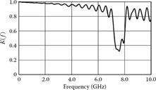
FIGURE 5.45
The amplitude-frequency response of the helical system containing a two-row comb-type dielectrical holder.

FIGURE 5.46
Asymmetrical meander system. 1: Meander electrode; 2: metalized substrate; 3: dielectrical holder; 4: field not covered by metal; 5: external shield.
5.5.4.1 Simulation of an Asymmetrical Meander System
The model of the asymmetrical meander system proposed in Staras, Skudutis, and Sakalauskas [24] and presented in Figure 5.46 was selected for investigation. The system consists of the meander electrode (1), a substrate (2) covered by a metal layer, and an external shield (5). Dielectrical sticks (3) are used for holding the meander electrodes. In order to reduce parasitic capacitances between the meander electrode and the metalized substrate, the metal layer is removed (from fields (4)) around the holding sticks.
The methodology of investigation of meander systems with the application of the MWS package is the same as that for investigation of helical systems: The draft of the system is composed using the internal graphical editor and input and output ports are specified. Methods developed in the application of the Microwave Office program package can be used for calculation of phase delay time and characteristic impedance.
With meander electrode width h = 8.5 mm, step of meander conductors L = 1 mm, width of conductors l = 0.5 mm, thickness of meander electrode t = 0.2 mm, gap between electrode and metalized substrate w1 = 0.2 mm, and gap between electrode and shield w2 = 0.1 mm, the calculated value of the retardation factor of the meander system was ≅10, and the characteristic impedance was ≅50 Ω [25].
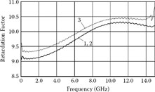
FIGURE 5.47
Retardation factor of the meander system (Figure 5.46) versus frequency at various values of relative dielectric permittivity of the substrate. 1: εr = 1; 2: εr = 4; 3: εr = 8.
The dispersion characteristics of the meander system and its amplitude-frequency responses are presented in Figures 5.47 and 5.48.
The dispersion characteristics (Figure 5.47) are of the same form as those obtained using the multiconductor line and experimental methods. Relatively great dispersion of phase delay time and the retardation factor is a characteristic feature of meander systems.
According to calculations, dispersion characteristics and amplitude-frequency responses only slightly depend on the dielectric permittivity of the substrate. At relative dielectric permittivity εr = 1 and εr = 4, characteristics coincide. At εr = 8, the retardation factor becomes approximately 2.5% higher, and the width of the pass-band becomes approximately 0.5 GHz lower. These results coincide with the idea [24] about the small influence of the substrate material on properties of the considered meander system.
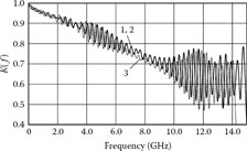
FIGURE 5.48
Amplitude-frequency responses of the meander system (Figure 5.46) at various values of relative dielectric permittivity of the substrate. 1: εr = 1; 2: εr = 4; 3: εr = 8.
Ripples of the amplitude-frequency responses in Figure 5.48 are caused by multiple reflections from output and input of the system. The distances between maximal or minimal values of amplitude-frequency responses are inversely proportional to the phase delay time and can be found using Equation (5.10). Reflections increase with frequency as a result of variation of characteristic impedance of the meander line and an increase of reactivities at the ends of the system. The influence of the end effects can be reduced by application of matching line sections as in helical systems. According to Figure 5.48, the meander conductors act as the quarter-wave length impedance transformers at frequencies close to 8 GHz.
5.5.4.2 Simulation of a Symmetrical Meander System
The model of the symmetrical meander system is shown in Figure 5.49. It consists of two parts. One is the same as the asymmetrical system presented in Figure 5.47, except for frontal part of the external shield. The other part is like a mirror reflection of the first part. The distance between meander electrodes is two times greater than the gap between the meander electrode and the external shield in Figure 5.47.
It is known that, at the odd mode, properties of the symmetrical system do not change if the symmetry plane is changed by the electrical wall. Thus, properties of the asymmetrical (Figure 5.47) and symmetrical (Figure 5.49) systems must be the same.
The circuit diagram used for investigation of the symmetrical meander system is presented in Figure 5.50. To excite the odd mode, sources generating voltages of opposite polarities are used in the circuit. Resistances ZG and ZL are equal to characteristic impedance of the asymmetrical meander line at low frequency.
The calculated value of the retardation factor of the symmetrical meander system is slightly higher; its characteristic impedance is slightly less. The amplitude-frequency responses of the systems (Figure 5.51) are similar, but do not coincide. The width of the pass-band of the symmetrical system is slightly greater.

FIGURE 5.49
The model of the symmetrical meander system. 1 and 2: Meander electrodes.
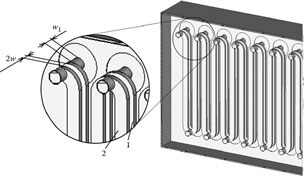
FIGURE 5.50
The circuit diagram for investigation of the meander system.
Thus, errors appear at calculations of characteristics at small cross-section dimensions of the systems. These errors can be reduced by refining of the mesh.
5.5.4.3 Simulation of an Axially Symmetrical Meander System
In addition to meander systems with plane symmetry, axially symmetrical systems are known. Acording to Staras et al. [2] and Section 2.7, at small distances between meander electrodes, properties of axially symmetrical meander systems differ from those of meander systems with plane symmetry.
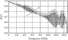
FIGURE 5.51
Amplitude-frequency responses of meander systems. 1: Asymmetrical; 2: symmetrical.
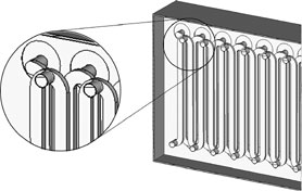
FIGURE 5.52
The model of the axially symmetrical meander system.
A higher retardation factor, less dispersion, and higher characteristic impedance are characteristic features of axially symmetrical systems.
The model of the axially symmetrical meander system is presented in Figure 5.52. The system consists of two identical parts like the asymmetrical meander system (Figure 5.46), except for the frontal part of the external shield.
According to calculations, characteristic impedance of the considered meander system with plane symmetry was 47 Ω; at axial symmetry, it was 61 Ω. Dispersion characteristics of the systems are presented in Figure 5.53. According to this figure, the retardation factor of the axially symmetrical meander system in the low-frequency range is aproximately 30% higher than that of the system with plane symmetry. The differences in properties of the systems are related to interaction of electromagnetic fields in the systems [2]. At input voltages of opposite polarities, currents along opposite conductors of meander electrodes flow in the same direction. As a result, the distributed inductivities of meander electrodes are greater, and values of characteristic impedance and retardation factor are higher.

FIGURE 5.53
Retardation factors of meander systems versus frequency. 1: At plane symmetry of meander electrodes; 2: at axial symmetry.

FIGURE 5.54
Amplitude-frequency responses of meander systems at plane symmetry (curve 1) and at axial symmetry (curve 2).
The amplitude-frequency responses of the systems with plane and axial symmetry are presented in Figure 5.54. The figure shows that the ripples of the amplitude-frequency response of the axially symmetrical meander system in the low-frequency range are small. Thus, the axially symmetrical meander system is better matched with the signal path at low frequencies.
To illustrate the dependencies of frequency properties of symmetrical meander systems on the distances between the meander electrodes, characteristics of the systems with plane and axial symmetry at increased distance between meander electrodes are presented in Figures 5.55 and 5.56. Comparison of characteristics in these figures with those in Figures 5.53 and 5.54 shows that, at increased distance between the electrodes, characteristics of the axially symmetrical meander systems approach the characteristics of systems with plane symmetry.
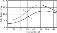
FIGURE 5.55
Retardation factors of meander systems at increased distance between meander electrodes (2w = 0.7 mm). 1: At plane symmetry of meander electrodes; 2: at axial symmetry.
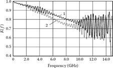
FIGURE 5.56
Amplitude-frequency responses of meander systems with plane symmetry (curve 1); axial symmetry (curve 2) at increased distance between meander electrodes (2w = 0.7 mm).
Thus, the MicroWave Studio software system can be successfully applied for simulation, investigation, and design of wide-band slow-wave devices.
The software packages Microwave Office and MicroWave Studio developed for analysis of electromagnetic fields and design of microwave devices can be successfully and effectively applied for simulation, analysis, and design of super-wide-band periodical slow-wave systems.
We developed circuits and methods for calculation of specific parameters and characteristics of the slow-wave systems, such as characteristic impedance, phase delay time, and the retardation factor.
Results of calculations obtained using the Microwave Office and MicroWave Studio packages confirmed general properties of twined helical, asymmetrical meander, and symmetrical meander systems discovered using other (electrodynamic, multiconductor line) methods.
Application of the versatile software for simulation of the slow-wave structures allows taking into account effects related to the limited length of the structures, reactivities at their ends, terminals, and other peculiarities of real structures.
The Microwave Office package has been developed for simulation, investigation, and design of planar structures. Difficulties related to simulation of three-dimensional elements of slow-wave structures arise in the application of this package.
Application of the MicroWave Studio package for simulation of slow-wave structures allows composing models of slow-wave systems that are close to real three-dimensional structures.
In the application of universal software packages developed for analysis of electromagnetic fields and design of microwave devices, the complex influence of various factors on characteristics of slow-wave systems is taken into account. Difficulties arise in the identification of the influence of particular factors and reasons for the peculiarities of integral characteristics.
1. Vainoris, Z., Kirvaitis, R., and Staras, S. 1986. Electrodynamic delay and deflection systems. Vilnius, Lithuania: Mokslas, 266. [In Russian.]
2. Staras, S. et al. 1993. Super-wide band tracts of the traveling-wave cathode-ray tubes. Vilnius, Lithuania: Technika, 360. [In Russian.]
3. Microwave Office design suite is the industry’s fastest growing microwave design platform and has revolutionized the communications design world by providing users with a superior choice. [interactive]. Viewed February 4, 2011 (http://web.awrcorp.com/Usa/Products/Microwave-Office).
4. Daskevicius, V., and Skudutis, J. 2000. Investigation of properties of helical delay system using package Microwave Office 2000. Electronics and Electrical Engineering 2 (25): 30–33. [In Lithuanian.]
5. Daskevicius, V., and Skudutis, J. 2000. Analysis of helical slow-wave system using Microwave Office package. Electronics and Communication 1 (8): 118–121. [In Russian.]
6. Skudutis, J., and Daskevicius, V. 2000. Investigation of the properties of the helical delay system using Microwave Office 2000 package. 7th Biennial Baltic Electronics Conference BEC’2000, Conference Proceedings, 269–272.
7. Skudutis, J., and Daskevicius, V. 2001. Investigation of properties of retard system of two input helices. Electronics and Electrical Engineering 5 (34): 32–37. [In Lithuanian.]
8. Skudutis, J., and Daskevicius, V. 2001. Investigation of twined helical system using package Microwave Office 2001. Electronics and Communication 10: 99–103. [In Russian.]
9. Correll, A., and Ronald, E. 1989. Traveling wave push-pull electron beam deflection structure having voltage gradient compensation. US Patent No. 4812707.
10. Skudutis, J., and Daskevicius, V. 2002. Investigation of the input impedance of retard and deflecting systems. Electronics and Electrical Engineering 7(42): 13–17. [In Lithuanian.]
11. Skudutis, J., and Daskevicius, V. 2002. Investigation of input impedance of helical slow-wave deflection system. Electronics and Communication 15: 150–153. [In Russian.l
12. Guillaume, A., and Loty, C. H. Perfectionnements aux lignes a retard. Brevet d’invertion No. 1465559 (France).
13. Vainoris, Z., Gerasimavicius, V., and Staras, S. 1970. Transition from coaxial to helical line in traveling-wave tube. Radioelectronics 8:259–262. [In Russian.]
14. Maceika, K., and Malisauskas, V. 1979. Resonances in helical slow-wave systems containing two shields. Radioelectronics 15 (2): 112–117. [In Russian.]
15. Skudutis, J., and Daskevicius, V. 2003. Investigation of influence of the shield on properties of a helical system. Electronics and Electrical Engineering 6 (48): 22–27. [In Lithuanian.]
16. Skudutis, J., Daskevicius, V., and Garsva, E. 2004. Experience in applying of Microwave Office program package to the delay system investigation. Electronics and Electrical Engineering 2 (51): 68–73. [In Lithuanian.]
17. Burokas, T., Daskevicius, V., Skudutis, J., and Staras, S. 2005. Simulation of the wide-band slow-wave structures using numerical methods. EUROCON 2005, Computer as a Tool, Belgrade, 1: 848–851.
18. Skudutis, J., and Daskevicius, V. 2004. Investigation of resonance suppression possibilities in a helical system. 9th Biennial Baltic Electronics Conference BEC’2004, Conference Proceedings, 125–128.
19. Dunham, M., and Hudson, C. Cavity resonance absorption in ultra-high bandwidth CRT deflection structure by a resistive load. US Patent No. 5210464.
20. Potapov, J. 2004. CST MicroWave Studio 5.0. EDA Expert #8 CHIP NEWS 7, 2004, 36–41.
21. Skudutis, J., and Daskevicius, V. 2006. Investigation of properties of helical slow-wave system using program package MicroWave Studio. Electronics and Electrical Engineering 1 (65): 38–42. [In Lithuanian.]
22. Staras, S., and Burokas, T. 2003. Properties of nonhomogeneous helical system. Electronics and Electrical Engineering 1 (43): 17–20. [In Lithuanian.]
23. Vainoris, Z., Skudutis, J., Stankunas, J., Cuplinskas, A., and Staras, S. 1984. Super-wide-band traveling-wave retard-deflecting system. USSR Invention Certificate No. 1114236. [In Russian.]
24. Staras, S., Skudutis, J., and Sakalauskas, J. 1990. Small-sized traveling-wave retard-deflecting system. USSR Invention Certificate No. 1598759. [In Russian.]
25. Skudutis, J., and Daskevicius, V. 2006. Investigation of meander delay system properties using the software package MicroWave Studio. Electronics and Electrical Engineering 8 (72): 11–14.
26. Staras, S., and Skudutis, J. 1999. Traveling-wave deflection systems. Software for Electrical Engineering and Design, WITPRESS, Southampton, Boston, 23–32.
27. Martavicius, R. 1996. Electrodynamic -plain retard systems for wide-band electronic devices. Vilnius, Lithuania: Technika, 264. [In Lithuanian.]
28. Daskevicius, V., Skudutis, J., and Staras, S. 2007. Simulation of the inhomogeneous meander line. Electronics and Electrical Engineering 2 (74): 37–40.
29. Kleiza, A., and Staras, S. 1999. Calculation of characteristic impedances of multiconductor. Electronics and Electrical Engineering 4 (22): 41–44. [In Lithuanian.]
30. Burokas, T., and Staras, S. 2004. Properties of helical and serpentine slow-wave systems containing dielectric holders. Electronics and Electrical Engineering 4 (53): 22–27. [In Lithuanian.]
31. Staras, S., and Burokas, T. 2004. Modeling and improvement of the traveling-wave deflection systems and their transitions. Electronics and Electrical Engineering 1 (50): 9–15. [In Lithuanian.]
32. Daskevicius, V., Skudutis, J., and Staras, S. 2007. Simulation and properties of the H-profile meander system. Electronics and Electrical Engineering 3 (75): 65–68.
33. Daskevicius, V., Skudutis, J., and Staras, S. 2008. Simulation of slow-wave structures using synergy of various methods. 11th Biennial Baltic Electronics Conference BEC’2008, Conference Proceedings, 95–98.
34. Staras, S., and Burokas, T. 2004. Simulation and properties of transitions to traveling-wave deflection systems. IEEE Transactions on Electron Devices 51 (7): 1049–1052.
35. Daskevicius, V., Skudutis, J., and Staras, S. 2008. Simulation of symmetrical and asymmetrically shielded helical lines. Electronics and Electrical Engineering 3 (83): 3–6.
36. Daskevicius, V., Skudutis, J., and Staras, S. 2009. Simulation of the axially symmetrical helical line. Electronics and Electrical Engineering 1 (89): 101–104.