
Investigation of Slow-Wave Structures Using Synergy of Various Methods
The principles and potentialities of electrodynamical, multiconductor line, and numerical methods for investigation of wide-band slow-wave systems were revealed in previous chapters. Using the multiconductor line method, we can relatively easily discover essential properties of the systems. On the other hand, in the application of this method, infinitively long models are used and end effects as well as transitions to the systems are not taken into account. Software packages based on numerical methods allow modeling structures that are close to real systems and finding their final characteristics. Unfortunately, in the simulation of complex structures, sometimes it is difficult to reveal reasons for nonuniformities of characteristics, find ways to improve the structures, and make optimal design decisions.
In this chapter, we present results of simulation of some special types of slow-wave systems (asymmetrical meander system, H-profile meander system, asymmetrically shielded and symmetrical helical systems) and propose the idea of application of synergy of various methods to investigation and design of wide-band slow-wave structures.
This chapter is based on results found in references 1,2,3,4,5,6.
6.1 Simulation of an Inhomogeneous Meander Line
Models of meander-type lines are proposed and their properties are described in references 7,8,9 and other books and papers. On the other hand, idealized models of the systems are usually used. Real meander systems are nonhomogeneous structures. Inhomogeneities appear due to dielectric holders, bending of the conductor of the meander electrode, errors of manufacturing of the system, and for other reasons.
Periodic inhomogeneities of wide-band helical and meander systems cause nonuniformities of their frequency characteristics.
Inhomogeneities of meander systems can be symmetrical or asymmetrical with respect to the longitudinal axis of the meander system. Only symmetrical inhomogeneities are usually taken into account in models of meander systems. The influence of asymmetrical inhomogeneities on properties of the meander systems was not investigated.
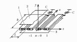
FIGURE 6.1
The model of the meander line containing capacitive asymmetrical inhomogeneities. 1: Conductor of the multiconductor line; 2 and 3: shields.
In this section, we analyze the influence of asymmetrical inhomogeneities, inhomogeneities that appear at the sides of the meander electrode due to bending of the conductor, and inhomogeneities at the ends of the electrode on characteristics of the meander system using the multiconductor line method and the Computer Simulation Technology (CST) Corporation software package MicroWave Studio [10].
6.1.1 Simulation of Asymmetrical Inhomogeneities
In order to reveal the influence of asymmetrical inhomogeneities, we can use the multiconductor line method. The model of the meander-type line is presented in Figure 6.1. The periodical asymmetrical inhomogeneities are modeled by capacitances connected to one side of the meander electrode.
Assuming that conductors are in the vacuumed space, using the quasi-TEM wave approximation and taking into account normal modes, we have the following expressions [7,8] for voltages and currents of the conductors in the multiconductor line:
(6.1) |
(6.2) |
where
Ai are amplitude coefficients
n is the number of the conductor of the multiconductor line
k = ω/c0 is the wave number
ω is the angular frequency
c0 is the light velocity in the free space
θ is the phase angle between the voltages on the adjacent conductors of the multiconductor line
ϒ(θ)and ϒ(θ + π) are characteristic admittances of the multiconductor line
The segment of the multiconductor line models the meander line (Figure 6.1) if the following boundary conditions are satisfied:
(6.3) |
(6.4) |
(6.5) |
and
(6.6) |
Substituting Equations (6.1) and (6.2) into Equations (6.3),(6.4),(6.5),(6.6), we arrive at a set of algebraic equations. Considering the set at zero determinant, we can find values of the retardation coefficient kR and frequency f
(6.7) |
(6.8) |
where vph is the phase velocity of the traveling wave, and L is the step of the conductors of the multiconductor line.
After that, we can find the input impedance of the meander line. It is dependent on the coordinate x. At x = 0, according to Equations (6.1) and (6.2),
(6.9) |
The dispersion characteristics of the meander line, calculated using the multiconductor line method, are presented in Figure 6.2. The numerical finite difference method is used for calculation of characteristic admittances and corresponding characteristic impedances Z(0) = 1/ϒ(0), Z(π) = 1/ϒ(π).
According to Figure 6.2, at C = 0, the graph kR(f) is continuous in the phase angle range from 0 to π. At C ≠ 0, the stop-band exists at θ = 2πfkRL/C = π/2. The width of the stop-band increases when the values of the periodic capacitances C increase.
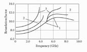
FIGURE 6.2
Retardation factor versus frequency at Z(0) = 100 Ω, Z(π) = 50 Ω.1: C = 0; 2: C = 0.1 pF; 3: C = 0.5 pF.
In order to verify the idea about the appearance of the stop-band of the meander line containing asymmetrical inhomogeneities, at θ ≅ π/2, the CST MicroWave Studio software system was used. The meander electrode, placed in the shield with a rectangular cross section, was considered. When the gap between the meander electrode and the shield at one side of the meander electrode is reduced with respect to the gap at the other side, the nonuniformity of the transfer characteristic of the meander line appears at frequencies corresponding to θ ≅ π/2 (Figure 6.3).
According to Staras and Burokas [11], the stop-band of the meander system, containing symmetrical inhomogeneities, exists at θ ≅ π. Then the period of inhomogeneities equals half of the meander period (the length h of the segment of the multiconductor line in Figure 6.1). We can explain the appearance of the stop-band at θ ≅ π/2 in the case of the meander system containing asymmetrical inhomogeneities, taking into account that the period of the system becomes equal to 2h. As the period of inhomogeneities becomes twice as long, the stop-band appears at twice as low frequencies. In the same way, it is possible to explain the appearance of the stop-band at θ ≅ π/2 in meander systems with different dimensions of neighboring conductors [9].

FIGURE 6.3
The amplitude-frequency response of the meander line (1) containing a meander electrode symmetrical with respect to the shield with rectangular cross section, and (2) meander electrode, shifted in the plane of the electrode with respect to the shield.
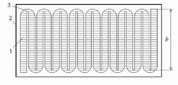
FIGURE 6.4
The amplitude-frequency response of the meander line. 1: With the constant width of the meander conductor; 2: with a reduced width of the conductor at the sides of the electrode.
6.1.2 Simulation of Inhomogeneities at the Sides of the Meander Electrode
Periodic inhomogeneities at the sides of the meander electrode exist due to change of direction of the conductor and spread of the electric field. In order to decrease the inhomogeneities caused by the spread of the field, the width of the conductor must be reduced. This idea was verified using the CST MicroWave Studio software. The transfer characteristic of the meander system containing the meander electrode with a constant width of the conductor is represented by curve 1 in Figure 6.4. Curve 2 corresponds to the system with a reduced width of the conductor at the sides of the meander electrode (Figure 6.5).
According to Figure 6.4, the amplitude response of the meander line can be really improved using the modified meander electrode (Figure 6.5).
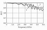
FIGURE 6.5
The view of the meander line. 1: Meander electrode; 2: shield; 3: the part of the meander conductor with reduced width.
Infinitely long systems are modeled using the multiconductor line method. The real systems have limited lengths, and the conditions of the last rods of meanders at the ends of the lines are different with respect to the other rods. Thus, inhomogeneities of the signal path at the ends of the systems appear. These inhomogeneities can be considered as inhomogeneities of the terminals the [12,13].
According to experimental investigations [8], inhomogeneities of the terminals can be reduced at smaller width of conductors at the ends of slow-wave systems. Simulation [14] and calculations using Microwave Office [15] confirmed the propriety of this idea.
According to simulation realized using the CST MicroWave Studio, the amplitude-frequency response of the signal path containing the meander line is dependent on the cross-section dimensions of the terminal rods, their length, and other dimensions of the meander line.
The amplitude-frequency responses of the signal path containing the meander line at different widths of the terminal rods are presented in Figure 6.6. According to the responses, it is necessary to widen terminal rods in order to improve the amplitude-frequency characteristic of the meander line.
The amplitude-frequency responses of the signal path with the meander line at different lengths of the terminal rods are presented in Figure 6.7. According to the figure, the frequency of the best matching of the signal path is strongly dependent on the length of the terminal rods. At length h, the best matching is realized at phase angle θ ≅ π/2 and frequency f≅ 1/(4td), where td is the delay time of the electromagnetic wave along the terminal rod. Increasing the rods, we can shift down the frequency of the best match.
We can explain the latter statements by taking into account that the terminal rods act as quarter-wave-length transformers. As the characteristic impedance of the meander line decreases from Z(0) to Z(π) with phase angle θ increasing from 0 to π/2, the characteristic impedance of the terminal rods Zc must be less than Z(0) = ZCn, where ZCn is the nominal characteristic impedance of the signal path. For this reason, better matching can be achieved at widened terminal rods.
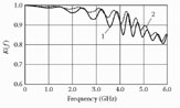
FIGURE 6.6
The amplitude-frequency responses of the signal path containing the meander line (1) at not changed and (2) at widened terminal rods.
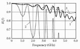
FIGURE 6.7
The transfer characteristics of the meander line at the different lengths b of the terminal rods. 1: b = h; 2:b = 0.7 h; 3: b = 1.25 h,
Finally, it is important to note that using quarter-wave-length transformers, we can improve matching of the meander system with the signal path and improve the transfer properties of meander systems; however, this way does not help to improve properties of traveling-wave deflection systems and other devices, where the best transfer of signals to the input of the meander system is necessary [14].
6.2 Simulation and Properties of the H-Profile Meander System
The pass-band of meander systems depends on dispersion of the retardation factor and variation of characteristic impedance with frequency [8]. In order to widen the pass-band and reduce linear distortions of signals, we must reduce the electromagnetic coupling between the parts of the meander conductor in the peripheral parts of the meander electrode where the phase angle between voltages on neighboring conductors is maximal. The coupling can be reduced by bending the neighboring parts of the meander electrode in opposite directions at the sides of the electrode. The cross section of the modified meander structure is presented in Figure 6.8(a). Figure 6.8(b) illustrates the simplified configuration of the H-profile meander electrode.
In this section, based on Potapov [10], we will use the multiconductor line method and the CST MicroWave Studio software package for simulation of the H-profile meander system in order to reveal its properties.
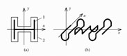
FIGURE 6.8
(a) The view of the H-profile meander system (1: meander electrode; 2: shield) and (b) the simplified view of the meander electrode.
6.2.1 Simulation Using the Multiconductor Line Method
In order to verify the idea that reducing the coupling of the lateral parts of the meander electrode can help to improve characteristics of the meander system, we used the model presented in Figure 6.9. It consists of three segments of the multiconductor line. The lateral segments are different with respect to the central part.
Assuming that conductors are in the vacuumed space and using the quasi-TEM wave approximation, we have the following expressions [8] for voltages and currents of the conductors in the multiconductor line:
(6.10) |
(6.11) |
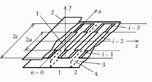
FIGURE 6.9
The model of the meander system. 1: Conductor of the multiconductor line; 2 and 3: shields; 4: shielding wall.
where i is the number or the segment of the multiconductor line, and n is the number of the conductor of the line.
The voltages and currents must satisfy boundary conditions at x = -a and x = a:
(6.12) |
(6.13) |
(6.14) |
and
(6.15) |
The system of multiconductor lines models the meander line if the following boundary conditions are satisfied:
(6.16) |
(6.17) |
(6.18) |
and
(6.19) |
Substituting Equations (6.10) and (6.11) into Equations (6.12)-(6.19), we arrive at a set of algebraic equations. Considering the set at zero determinant, we can find values of the retardation factor kR and frequency f using Equations (6.7) and (6.8). Then, we can find the input impedance of the meander line, which is dependent on the coordinate x as in other nonhomogeneous systems. At x = 0, according to Equations (6.10) and (6.11),
(6.20) |
The numerical finite difference method was used for calculation of characteristic admittances and corresponding characteristic impedances of the sections of the multiconductor line. In order to take into account that coupling of lateral parts of the meander electrode in the H-profile meander system is reduced, during calculations of characteristic admittances of peripheral sections of the multiconductor line, we admitted that the shielding walls (Figure 6.9) are far from the conductors of the line.
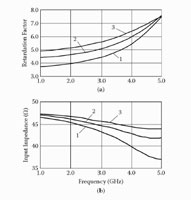
FIGURE 6.10
(a) Retardation factor and (b) input impedance of the meander system versus frequency at 2c/L = 7.5, Z2(0) = 57 Ω, Z2(π) = 36.5 Ω, Z1(0) = Z3(0) = 52 Ω, Z1(π) = Z3(π) = 36.5 Ω, and different widths (c - a) of the lateral parts of the meander electrode. 1: (c - a) = 0; 2: (c - a) = a = 0.5c; 3: (c - a) = 0.85c.
Characteristics of the meander structure, calculated using the model presented in Figure 6.9, are shown in Figure 6.10. According to them, reducing the coupling of conductors at the lateral parts of the meander electrode by widening the lateral parts of the electrode and narrowing down its central part allow us to reduce dispersion of retardation and variation of input impedance. Thus, there are possibilities to improve properties of the meander system using the H-type profile.
6.2.2 Simulation Using the MicroWave Studio Software Package
The model used, based on multiconductor lines, does not take into account that bending of the lateral parts of the meander electrode in the H-profile meander system causes a change of the period of the meander electrode. The system becomes a nonhomogeneous structure and its period becomes twice as long. In order to verify the discovered properties of the system and reveal effects caused by inhomogeneities and change of the period, we used the software package MicroWave Studio.
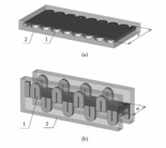
FIGURE 6.11
The flat (a) and H-profile (b) meander systems. 1: Meander electrode; 2: shield.
The model of flat and H-profile meander systems is presented in Figure 6.11. Applying the program package graphical editor, the system structure model was drawn and the ports of the signal source and load were indicated.
The frequency characteristics of flat and H-profile meander systems (retardation factor versus frequency and amplitude-frequency response) are presented in Figure 6.12(a, b). According to the figure, using bent lateral parts of the meander electrode, we can really reduce the dispersion of retardation and phase distortions in the meander system.
Analyzing the H-profile meander delay system properties in a wider frequency range, we can see that the stop-band appears at a frequency above 5 GHz. It is known [11,16] that the stop-band usually exists at the phase angle θ ≅ π in meander systems. For the investigated systems, it would be about 10 GHz. Since the period of the H-profile meander line is twice as great, the stop-band appears at θ ≅ π/2 and at an approximately twice as low frequency (i.e., near frequency f ≅ 5 GHz).
Because of dispersion, the upper limit of the pass-band of a meander system usually is less than the frequency, corresponding to θ ≅ π/2. Taking this into account, here we will not consider questions related to the stop-band in more detail.
The amplitude-frequency responses of the signal paths containing meander systems are presented in Figure 6.12(b). Oscillations (ripples) of the characteristics are caused by reflections from the terminals of the systems. They increase with frequency because characteristic impedances of the systems decrease with frequency (Figure 6.10b) and the influence of reactances at the terminals increases. The period of the ripples (in the frequency domain) is related to the delay time (Δf≅ 1/2td, where Δf is the period of the ripples and td is the delay time).
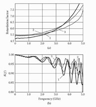
FIGURE 6.12
(a) Retardation factor and (b) transfer factor modulus versus frequency. 1: Flat meander system (Z(0) = 46 Ω); 2: H-profile meander system at a = 0.5c (Z(0) = 47 Ω); 3: H-profile meander system at a = 0.25c (Z(0) = 47 Ω).
Additionally, it is important to notice that nonuniformities of amplitude-frequency responses depend on the type of meander electrode. By narrowing the central part of the electrode and widening the bent lateral parts, we can reduce amplitudes of the ripples.
Thus, according to the results obtained using the multiconductor line method and the MicroWave Studio software package, the H-profile meander system has advantages with respect to the simple flat meander system. Furthermore, additional improvements to the H-profile system are possible.
The H-profile meander system is an inhomogeneous structure. The characteristic impedance changes along the conductor of the meander electrode. In order to reduce the ripples of the transfer characteristic, we must reduce the periodic variation of the characteristic impedance [17].
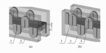
FIGURE 6.13
(a) Thinned and (b) narrowed meander conductor of the H-profile system. 1: Meander electrode; 2: shield; 3: lateral (loop) part of the meander electrode.
The characteristic impedance Z2(π) = 1/ϒ2(π), corresponding to the central part of the system, is less than Z1(π) = 1/ϒ1(π) and Z3(π) = 1/ϒ3(π). In order to reduce the periodic variation of the characteristic impedance, we must reduce the difference between Z2(π) and Z1(π) = Z3(π).
Also, according to the previous section, periodic inhomogeneities of the characteristic impedance of a meander system at a constant cross section of the conductor appear at the lateral sides of the meander electrode (at the ends of the meander loops) as a result of dissipation of the electrical field.
We can reduce the change of the characteristic impedance Zi(π), reducing the thickness of the conductor in the central part of the system (Figure 6.13a). The periodic reactances at the loops can be reduced by narrowing the conductor (Figure 6.13b). The amplitude-frequency responses, presented in Figure 6.14, illustrate that the mentioned means are effective. The ripples of curve 3 are considerably less with respect to curve 1.

FIGURE 6.14
The amplitude-frequency response of the signal path containing the H-profile meander system at a = 0.5c. 1: Constant cross section of conductor; 2: narrowed conductor at the lateral sides of the meander electrode; 3: thinned conductor in the central part and narrowed at the sides of the electrode.
The presented results confirm that, using the H-profile, we can comparatively simply improve characteristics of the meander line.
6.3 Simulation of Symmetrically and Asymmetrically Shielded Helical Lines
Usually, symmetrically shielded helical systems are considered and applied in electronic devices. In addition to them, almost unshielded helices are sometimes used. For example, a symmetrical system consisting of two helices can be used for deflection of the electronic beam in traveling-wave cathode-ray tubes. The cross section of the system is presented in Figure 6.15(a). When the odd electromagnetic wave is excited, the properties of such a symmetrical system are identical to the properties of the system, consisting of a helix and a shield (Figure 6.15b).
There is a lack of information about the properties of unshielded symmetrical and asymmetrically shielded asymmetrical helical systems. For this reason, we present models and results of simulation of the mentioned systems. The multiconductor line method and the CST software package MicroWave Studio are used for simulation and analysis.
6.3.1 Simulation Using the Multiconductor Line Method
In order to reveal the general properties of the systems (Figure 6.15), we will use the multiconductor line method. The model of the asymmetrical system (Figure 6.15b) is presented in Figure 6.16. It consists of the two-row multiconductor line and shields.
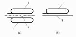
FIGURE 6.15
(a) The cross-sections of symmetrical and (b) asymmetrically shielded helical systems. 1 and 2: Helix; 3: electron beam; 4: shield.

FIGURE 6.16
(a) The model of the asymmetrical helical line and (b) the cross section of the multiconductor line. 1 and 2: Conductors of the two-row multiconductor line; 3 and 4: shields.
Using the quasi-TEM approximation and taking into account normal modes, we have the following expressions for voltages and currents of the conductors in the vacuumed line:
(6.21) |
(6.22) |
where m is the number of the row of the multiconductor line, n is the number of the conductor in the row, and ϒm(π, θ) and ϒm(0,θ) are characteristic admittances of the line.
The section of the multiconductor line models the helical system if these boundary conditions are satisfied at x = 0 and x = h:
(6.23) |
(6.24) |
(6.25) |
and
(6.26) |
Substituting Equations (6.21) and (6.22) into Equations (6.23)-(6.26), we arrive at a set of algebraic equations. Solving the set, we can derive the following dispersion equation:
(6.27) |
where ϒm0 = ϒm(0, θ), ϒmπ = ϒm(π, θ).
Solving the dispersion equation, we can find values of phase angle θ corresponding to selected values of the wave number k. Then, we can find values of the retardation factor kR and frequency f using Equations (6.7) and (6.8).
During calculations, values of characteristic impedances ϒm(π, θ) and ϒm(0,θ) can be found using the following formula [7,8]:
(6.28) |
where j = π,0. The finite difference or finite element method can be used for calculation of characteristic admittances ϒ(π,0), ϒ(π,π), ϒ(0,0), and ϒ(0,π) [18,19].
The input impedance of the system at asymmetrically positioned shields is dependent on the coordinate x. At x = 0, according to Equations (6.21) and (6.22),
(6.29) |
Thus,
(6.30) |
At low frequency, when kh → 0 and θ → 0, we can simplify the dispersion equation and obtain this expression for the retardation factor:
(6.31) |
According to Equation (6.31), when the distance between the helix and shields is constant along the helix wires and ϒ10 = ϒ20 = ϒ0, ϒlπ, = ϒ2π = ϒπ, the retardation factor is given by
At high frequency, when the electromagnetic field becomes concentrated at the helix conductor and characteristic impedances approach each other (ϒ10 ≅ ϒ1π ≅ ϒ20 ≅ ϒ2π), the retardation factor is determined by the length 2h and the step L of helix wires:
(6.32) |
Thus, at a constant distance between the helix and the shields, the retardation factor at low frequency is less than at high frequency. Analyzing Equation (6.31), we see that the retardation factor at low frequency increases if the distance between the helix and the upper shield (Figure 6.16) increases (ϒ10 and ϒ1π increase with respect to ϒ20 and ϒ2π). Thus, at asymmetrical disposition of shields or using the asymmetrically shielded asymmetrical helix system (Figure 6.15b), as well as the symmetrical system (Figure 6.15a), we can reduce dispersion of retardation with respect to dispersion in the asymmetrical helical system, containing the shield at constant distance from the helix.
Calculations of characteristics confirmed the latter idea. As an example, a set of characteristics of the asymmetrical system (retardation factor and input impedance versus frequency) is presented in Figure 6.17. According to Figure 6.17(a), by the shield approaching one side of a helix (Figure 6.15b) or reducing the distance between helices in the symmetrical system (Figure 6.15a), we can control and reduce the dispersion of retardation and dispersion of phase velocity of the electromagnetic wave. At less of a gap between a helix and a shield or less distance between the helices, the characteristic impedance becomes lower and less dependent on frequency.
Therefore, there is a possibility to control the dispersion properties of the symmetrical and asymmetrical helical systems (Figure 6.15) and reduce the phase-frequency distortions of propagating signals at a relatively high characteristic impedance of the retard system.
6.3.2 Simulation Using the MicroWave Studio Package
The multiconductor line method allows us to model infinitely long slow-wave systems. Additionally, changes of characteristic impedances of vertical parts of the helical wires (Figure 6.15) are not taken into account when the simplest model (Figure 6.16) is used. In order to verify the conclusions based on the multiconductor method, the CST software package MicroWave Studio was used for simulation of the systems presented in Figure 6.15.

FIGURE 6.17
(a) Retardation factor and (b) input impedance versus frequency at h = 10, L = 2, l = 1, w1 = 10, w = 1.5. 1: w2 = 2; 2: w2 = 1.5; 3: w2 = 1; 4: w2 = 0.75; 5: w2 = 0.5 mm.
The models of the symmetrical and asymmetrical helical systems, developed using the CST MicroWave Studio graphical editor, are presented in Figures 6.18 and 6.19. The calculation methodology of characteristics of slow-wave structures using MicroWave Studio is described in Skudutis and Daskevicius [20].
The set of curves illustrating dispersion properties of the asymmetrical helical system (Figure 6.19) is presented in Figure 6.20. Characteristics are similar to the curves presented in Figure 6.17(a). Small differences are related to simplifications made when composing the model (Figure 6.16) based on the multiconductor lines.
The approximate values of characteristic impedance in the low-frequency region determined using the MicroWave Studio package are lower (by 10–25%) with respect to the values obtained using the multiconductor method. The differences between the results increase if the gap between the helix and the shield increases. Analysis of calculation results revealed the cause of the differences. They are related to the scatter of the electric field and increase of influence of capacitances at the ends of the system when removing a shield from one side of the system.
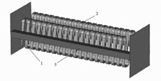
FIGURE 6.18
The model of the symmetrical helical system. 1 and 2: Helices; 3: dielectrical holder.
The amplitude-frequency responses of the asymmetrical system are presented in Figure 6.21. According to curve 2 (obtained at minimal dispersion of retardation), amplitude-frequency distortions in the helical system with relatively high characteristic impedance 2 × 100 Ω are less than 3 dB in the frequency range from 0 to 3 GHz.
According to analysis, sometimes we can obtain desirable characteristics of the systems using effects that appear due to inhomogeneities.
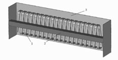
FIGURE 6.19
The model of the asymmetrical helical system. 1: Helix; 2: dielectrical holder, 3: shield.
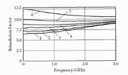
FIGURE 6.20
Retardation factor versus frequency at h = 10, L = 2,1 = 1, w1 = 10, w = 1.5. 1: w2 = 2; 2: w2 = 1.5; 3: w2 = 1; 4: w2 = 0.75; 5: w2 = 0.5; 6: w2 = 0.25 mm.
6.4 Simulation of the Axially Symmetrical Helical Line
In the central part of the helical system with the plane, symmetry currents flow in opposite directions. In the central part of the axially symmetrical helical system, currents flow in the same direction. As a result of this, the magnetic flux, the distributed inductivity, and the characteristic impedance of the axially symmetrical system are higher.
In order to reveal properties and possible advantages of axially symmetrical helical systems, we propose its models and present results of simulation in this section. As in previous sections of this chapter, the multiconductor line method and the CST software package MicroWave Studio are used for simulation and analysis.
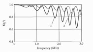
FIGURE 6.21
The amplitude-frequency responses of the asymmetrical helical line at h = 10, L = 2, l= 1, w1 = 10, w = 1.5. 1: w2 = 2; 2: w2 = 0.5 mm.
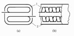
FIGURE 6.22
Axially symmetrical helical line. 1: Helix; 2: shield.
6.4.1 Simulation Using the Multiconductor Line Method
In order to reveal general properties of the axially symmetrical helical system (Figure 6.22), we will use the multiconductor line method. The model of the system (Figure 6.22) is presented in Figure 6.23. It consists of the four-row multiconductor line and shields. The space between conductors is vacuumed.
Using the quasi-TEM approximation and taking into account normal modes, we have the following expressions for voltages and currents of the conductors in the line:
(6.33) |
(6.34) |
(6.35) |
and
(6.36) |
where
ϒ1E0 = ϒ1E(0,θ), y1Eπ = ϒ1E(π,θ), ϒ2Eπ = ϒ2E(0,θ), and ϒ2Eπ = ϒ2E(π,θ) are characteristic admittances of the line at the electrical wall in the plane x0z
ϒ1M0 = ϒ1M(0,θ), ϒ1Mπ = ϒ1Mπ(π, θ), ϒ2M0 = ϒ2M(0,θ), and ϒ2Mπ = ϒ2Mπ(π, θ) are characteristic admittances of the multiconductor line at the magnetic wall in the plane x0z
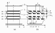
FIGURE 6.23
The model of the axially symmetrical helical line. 1 and 2: Conductors of the multiconductor line; 3: shield.
We can assume that the type of wall does not influence the admittances of the outside rows with m = 1 and m = 4. Then, ϒ1E0 = ϒ1M0 = ϒ10 and ϒ1E0 = ϒ10π = ϒ1π.
The section of the multiconductor line models the axially symmetrical helical system if these symmetry and boundary conditions are satisfied:
(6.37) |
(6.38) |
(6.39) |
(6.40) |
(6.41) |
and
(6.42) |
Substituting Equations (6.33) and (6.34) into Equations (6.37),(6.38),(6.39),(6.40),(6.41),(6.42), we arrive at a set of algebraic equations. Solving the set, we can derive the following dispersion equation:
(6.43) |
Solving the dispersion equation, we can find values of phase angle θ corresponding to selected values of the wave number k. Then, we can find values of the retardation factor kR and frequency f using Equations (6.7) and (6.8).
The input impedance of the system is dependent on the coordinate x. At x = 0, according to Equations (6.33) and (6.34),
(6.44) |
Thus,
(6.45) |
where
and
As an example, a set of characteristics of the axially symmetrical system (retardation factor and input impedance versus frequency) is presented in Figure 6.24.
According to Staras et al. [8], the retardation factor of a single, unshielded helix at low frequency is low. It increases with frequency and approaches the structural retardation factor kRs = 2h/L (where 2h corresponds to the turn length and L is the step of the helical turns).
The characteristic impedance of the axially symmetrical helical structure periodically changes along the helical wire. Using properties of electrodynamical structures with periodical inhomogeneities [19,20,21], it is possible to increase the retardation factor of the axially symmetrical line at low frequency, approach the structural retardation, and reduce the dispersion of the slow electromagnetic wave in the line (Figure 6.24a). According to Equation (6.43), the retardation factor at low frequency becomes equal to the structural retardation if ϒ1π = 2ϒ10 = ϒ2Eπ = 2ϒ2Mπ = 2ϒ and ϒ2M0 = 0.
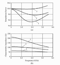
FIGURE 6.24
(a) Retardation factor and (b) input impedance versus frequency at h = 10, L = 2, l = 1, p = 0.25 mm. 1: w1 = w= w2 =1;2: w1 = w = 0.5, w2 = 1;3: w1 = 1.25, w2 = 0.25, w2 = 0.25. Dimensions = millimeters.
The input impedance of the axially symmetrical system (Figure 6.24b) decreases if the distance between helices decreases, and it really can be sufficiently higher than the input impedance of the helical line with plane symmetry.
6.4.2 Simulation Using the MicroWave Studio Package
In order to verify the conclusions based on the multiconductor method, the CST software package MicroWave Studio was used for simulation of the system presented in Figure 6.22. The model of symmetrical helical systems with axial symmetry, developed using the CST MicroWave Studio graphical editor, is presented in Figure 6.25. The calculation methodology of characteristics of slow-wave structures using this package is described in the Section 6.3.

FIGURE 6.25
The model of the symmetrical helical system with axial symmetry. 1: Helix; 2: shield; 3: holder; 4: port.
The set of curves illustrating dispersion properties of the helical system with axial symmetry (Figure 6.25) is presented in Figure 6.26. Characteristics confirm that there are possibilities to increase the retardation factor at low frequency and reduce dispersion. According to Figure 6.26, the dispersion of retardation is less than 3–4%.
The values of the system input impedances in the low-frequency region are 212, 110, and 63 Ω, according to Figure 6.24(b), and 173, 98, and 59 Ω as a result of calculations using CST MicroWave Studio. Thus, the values of the input impedance in the low-frequency range determined using this package are lower (by 6–18%) with respect to the values when the multiconductor line method was used.
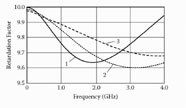
FIGURE 6.26
Retardation factor versus frequency at h = 10, L = 2, l = 1, p = 0.25 mm. 1: w1 = w = w2 = 1; 2: w1 = w = w2 = 0.5; 3: w1 = w = w2 = 0.25. Dimensions = millimeters.

FIGURE 6.27
The amplitude-frequency responses of the helical system with axial symmetry at h = 10, L = 2, l = 1, p = 0.25 mm. l: w1 = w = w2 = l; 2:w1 = w = w2 = 0.5; 3: w1 = 0, w = w2 = 0.25. Dimensions = millimeters.
The differences in values of the retardation factor and input impedances can be explained by taking into account that the analyzed system investigated by the MicroWave Studio package was not infinitely long, but rather has real length and input and output ports (Figure 6.25).
The transfer characteristics of the axially symmetrical helical system (with length of 40 mm) are presented in Figure 6.27. Oscillations of characteristics are caused by reflections from the ports of the system. They increase with frequency because the input impedance of the system decreases with frequency (Figure 6.24b). The period of the ripples (in the frequency domain) is related to the delay time in the system (Δf ≅ 1/2td, where Δf is the period of the ripples and td is the delay time).
According to Figure 6.27, amplitude-frequency distortions are less than 3 dB in the frequency range from 0 to 4 GHz. A comparison of these results with those obtained in Section 6.3 shows that, at properly selected dimensions, axially symmetrical helical systems ensure a wider pass-band with respect to plane symmetry systems.
Using synergy of various methods for simulation of slow-wave structures, we can improve analysis and design of slow-wave structures. Applying the multiconductor line method in conjunction with the CST MicroWave Studio software, we examined some complicated versions of meander and helical systems (asymmetrical meander system, H-profile meander system, asymmetrically shielded and symmetrical helical systems) and revealed their properties.
Asymmetrical inhomogeneities of the meander electrode cause nonuniformity of frequency characteristics of the meander system at phase angle θ = π/2 and frequency f 1/(4td, where td is delay time along a rod of the meander electrode. Frequency properties of meander systems can be improved and the distortions of signals can be reduced using modified meander electrodes. The terminal rods of the meander electrode act as quarter-wave length transformers. Changing their length, we can change the frequency at which the signal path is best matched.
Characteristics of the H-profile meander system are better with respect to the simple flat meander structure. We propose means for further improvement of the H-profile meander system, based on reduction of periodic inhomogeneities along the meander conductor.
We discovered properties of the symmetrical helical system and asymmetrical system containing the asymmetrical shield. Application of the multiconductor line method allowed us to show that there are possibilities to design simple helical symmetrical systems or asymmetrical systems having good dispersion properties and relatively high characteristic impedance. Simulation made using the package CST MicroWave Studio confirmed the properties of the systems discovered using the multiconductor line method.
We recommend using the synergy of the multiconductor line method and commercial packages for analysis and design of wide-band helical and meander structures. The multiconductor line method makes it relatively easy to obtain the desired properties of a structure. Modern commercial packages allow modeling the structures with real lengths and ports and can be used for the final analysis and design.
1. Daskevicius, V., Skudutis, J., and Staras, S. 2007. Simulation of the inhomogeneous meander line. Electronics and Electrical Engineering 2 (74): 37–40.
2. Burokas, T., Daskevicius, V., Skudutis, J., and Staras, S. 2006. Simulation and properties of the gutter-type meander systems. EMD 2006: XVI International Conference on Electromagnetic Disturbances: Proceedings, Kaunas, Lithuania, September 27-29,146–149.
3. Daskevicius, V., Skudutis, J., and Staras, S. 2007. Simulation and properties of the H-profile meander system. Electronics and Electrical Engineering 3 (75): 65–68.
4. Daskevicius, V., Skudutis, J., and Staras, S. 2008. Simulation of slow-wave structures using synergy of various methods. 11th Biennial Baltic Electronics Conference BEC’2008, Conference Proceedings, 95–98.
5. Daskevicius, V., Skudutis, J., and Staras, S. 2008. Simulation of symmetrical and asymmetrically shielded helical lines. Electronics and Electrical Engineering 3 (83): 3–6.
6. Daskevicius, V., Skudutis, J., and Staras, S. 2009. Simulation of the axially symmetrical helical line. Electronics and Electrical Engineering 1 (89): 101–104.
7. Vainoris, Z., Kirvaitis, R., and Staras, S. 1986. Electrodynamic delay and deflection systems. Vilnius, Lithuania: Mokslas, 266. [In Russian.]
8. Staras, S. et al. 1993. Super-wide band tracts of the traveling-wave cathode-ray tubes. Vilnius, Lithuania: Technika, 360. [In Russian.]
9. Martavicius, R. 1996. Electrodynamic plain retard systems for wide-band electronic devices. Vilnius, Lithuania: Technika, 264. [In Lithuanian.]
10. Potapov, J. CST MicroWave Studio 5.0. EDA Expert #8 CHIP NEWS 7 (1): 2004, 36–41.
11. Staras, S., and Burokas, T. 2005. Simulation of traveling-wave deflecting systems and deflection in traveling-wave cathode-ray tubes. EMD’ 2005, XV International Conference on Electromagnetic Disturbances, Proceedings, Kaunas, 99–104.
12. Guillaume, A., and Loty, C. H. Perfectionnements aux lignes a retard. Brevet d’invention No. 1,465,559 (France).
13. Cristie, A. B., and Correll, R. E. Traveling wave deflector for electron beams. US Patent No. 4093891.
14. Staras, S., and Burokas, T. 2004. Modeling and improvement of the traveling-wave deflection systems and their transitions. Electronics and Electrical Engineering 1 (50): 9–15. [In Lithuanian.]
15. Skudutis, J., and Daskevicius, V. 2002. Investigation of the input impedance of retard and deflecting systems. Electronics and Electrical Engineering 7 (42): 13–17. [In Lithuanian.]
16. Burokas, T., and Staras, S. 2004. Properties of helical and serpentine slow-wave systems containing dielectric holders. Electronics and Electrical Engineering 4 (53): 22–27. [In Lithuanian.]
17. Staras, S., and Burokas, T. 2004. Simulation and properties of transitions to traveling-wave deflection systems. IEEE Transactions on Electron Devices 51 (7): 1049–1052.
18. Kleiza, A., and Staras, S. 1999. Calculation of characteristic impedances of multiconductor lines. Electronics and Electrical Engineering 4:41–44. [In Lithuanian.]
19. Burokas, T., Daskevicius, V., Skudutis, J., and Staras, S. 2005. Simulation of the wide-band slow-wave structures using numerical methods. EUROCON 2005, Computer as a Tool. Belgrade, I: 848–851.
20. Skudutis, J., and Daskevicius, V. 2006. Investigation of properties of helical slow-wave system using program package MicroWave Studio. Electronics and Electrical Engineering 1 (65): 38–42. [In Lithuanian.]
21. Staras, S., and Burokas, T. 2003. Properties of nonhomogeneous helical system. Electronics and Electrical Engineering 1 (43): 17–20. [In Lithuanian.]