
Application of Slow-Wave Systems for Delay
Sometimes delay of electrical signals is necessary at transmission and processing of signals. Many types of delay devices have been developed. Miniaturized delay devices with wide-pass band, high linearity, and stability are necessary for signal synchronizations, analog, digital filtering, and other applications in modern electronic equipment [1,2,3,4].
Because of many advantages, meander delay lines are frequently used. The signal path of a modern meander delay line consists of a microstrip meander line and input and output ports (Figure 8.1). Microstrip meander lines are planar structures and modern technologies developed for integrated circuits can be used for fabrication of these lines.
Mathematical models are necessary in the simulation and computer-aided design of microstrip meander delay lines. General properties of meander slow-wave structures are described in references 5,6,7,8,9,10,11,12,13,14,15,16. Unfortunately, the developed models [5,6] are not adjustable for simulation of delay line structures containing package elements operating as shields above the meander electrodes, additional shielding strips among the conductors of signal meander electrodes, simulation of topological errors arising at manufacturing, etc. For these and other reasons, advanced models of microstrip meander lines are necessary.
The results published in references 17,18,19,20,21,22,23,24, 43, and 44 are generalized in this chapter. In the first section, we compose the advanced model of the ordinary microstrip meander delay lines and analyze the influence of topological errors on properties of the lines. In the second section, we present the model and analysis of the packaged meander system containing shields below the substrate and under the meander electrode. Questions related to characteristic and input impedances of meander lines are considered in the third section. Finally, in the last three sections, we compose the models and examine properties of wide-band microstrip meander lines containing additional strip-like and gutter-type shields.
8.1 Simulation of Meander Systems Containing Periodical Inhomogeneities
The main element of the microstrip meander line is the signal conductor made in the form of meander on the dielectric substrate (Figure 8.1). Usually, designers project meander conductor strips with constant width w. In manufacturing, errors of meander pattern appear, and the dimensions of the meander strips, gaps between them, and the step of conductors become scattered with respect to their mean values.
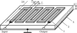
FIGURE 8.1
The structure of the ordinary microstrip meander delay line. 1: Signal conductor in the form of a meander; 2: dielectric substrate; 3: metal layer operating as a shield.
Coupling of straight parts of meander conductors causes dispersion of velocities of electromagnetic waves propagating in meander systems. Usually, the velocity of the wave in a meander system decreases with frequency. Interaction of electromagnetic fields of meander conductors is most intensive in the peripheral (lateral) parts of meander electrodes, where the phase angle between voltages on adjacent conductors and the strength of the electrical field between them are maximal. In order to reduce dispersion of retardation and phase delay time, the advanced pattern of the meander electrode (Figure 8.2) is sometimes used.

FIGURE 8.2
The microstrip meander line with improved pattern of the meander electrode. 1: Dielectric substrate; 2 and 3: peripheral segments of meander conductors; 4: central segments of the conductors; 5: longitudinal part of the meander electrode (the short-circuiter of multiconductor line conductors modeling the meander electrode).
According to Figure 8.2, the gaps between neighboring conductors in the peripheral parts of the meander electrode are increased. Then, the central part of the meander electrode is of the form of an ordinary multiconductor line containing a row of conducting strips with constant step. In the peripheral sections, meander conductors form a multiconductor line with periodically varying step of conducting strips.
Thus, the improved model of microstrip meander lines is desirable in the simulation of the influence of manufacturing errors and the search for optimal decisions in the design of wide-band delay lines with a small scatter of parameters and characteristics.
In this section, we compose the models of microstrip multiconductor lines with irregular step of conductors and microstrip meander delay lines containing periodical inhomogeneities and examine properties (phase delay time and input impedance frequency characteristics) of the lines.
8.1.1 Analysis of Multiconductor Line at Irregular Step of Conductors
Let us compose the model of the microstrip multiconductor line containing two conductors in a period (the line with periodically changing—for short to irregular—steps of conductors), examine the structure of the electric field in the line, and consider calculation of distributed capacitances of line conductors.
8.1.1.1 Model of Microstrip Multiconductor Line
The view of the cross section of the microstrip multiconductor line with irregular steps of conductors is presented in Figure 8.3. The conductors of the line are of the form of the strips with the same width, but gaps between adjacent conductors are different.
The theory of multiconductor lines is presented in Martavicius and Urbanavicius [25] and in Chapter 2 of this book. According to the Floquet theorem [26], at constant velocity of the space harmonic in the direction of the z axis, the phase angle between voltages or currents on adjacent conductors is dependent on the step of conductors. For instance, considering the zero space harmonic, we can write
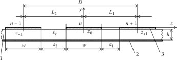
FIGURE 8.3
The cross section of the microstrip multiconductor line with irregular step of conductors. 1: Dielectric substrate; 2: shield; 3: line conductor in the form of a strip.
(8.1) |
where β0 is the phase constant of the zero space harmonic and L1 L2 are steps of conductors in the multiconductor line.
Using the multiconductor line method for simulation and design of the microstrip meander lines, we must determine characteristic impedances of conductors of the multiconductor lines. In order to develop the method for calculation of characteristic impedances, we must consider distribution of electric field and potential in the multiconductor line.
Electric potential in the multiconductor line is given by Martavicius [37]
Φ_(x,y,z)=(Acoskx+Bsinkx)∞∑q=−∞Φ_q(y)e−jβqz, |
(8.2) |
where A and B are amplitude coefficients, k=ω/√με
To find potentials on conductors with order numbers n, n + 1, and n -1, we must substitute coordinates z0 = nD/2, z±1 = z0±L1,2 of these conductors into Equation (8.2).
Conductors situated with periodically changing step can be considered as conductors following with the constant step L and periodical deviations ±ΔL, from this step. Then we can write the following:
(8.3) |
(8.4) |
and
(8.5) |
where D is the period of the multiconductor line.
Taking into account Equations (8.3),(8.4),(8.5), we can write the following expressions of potentials at the middles of the infinitely thin nth and (n ± l)-th conductors (strips):
Φ_(x,y,z)=(Acoskx+Bsinkx)∞∑q=−∞Φ_q(y)e−j(θ+2πNq)n |
(8.6) |
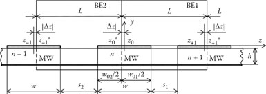
FIGURE 8.4
Positions of the magnetic walls in the cross section of the microstrip multiconductor line; MW: magnetic wall; BE1, BE2: basic elements of the multiconductor line.
and
Φ_(x,y,z±1)=(Acoskx+Bsinkx)∞∑q=−∞Φ_q(y)e−j(θ+2πNq)(n±1ΔLL). |
(8.7) |
According to Equation (8.6), the potential at the middle of the nth strip, as in ordinary multiconductor lines, is determined by superposition of normal electromagnetic waves. Expression (8.7) is complicated with respect to Equation (8.5). On the other hand, using the conception of basic elements (see Chapter 2), we can simplify Expression (8.7) and its interpretation, assuming that the multiplier n ± 1 - ΔL/L in the power index is an integer (ΔL/L = 0) and at the same time that the magnetic walls are shifted from the centers of the conductors in the direction of the wide gap (Figure 8.4).
Assuming that the shift is Δz = ΔL/2, we can use the transferred coordinates Z0*, z±1*= Z0*±L of conductors of the multiconductor line. With the indicated assumptions, distribution of the electric field in the basic element BEI with less gap s1 between conductors is the same as in the multiconductor line with conductors of the width w01 following with the constant step L1. Distribution of the field in the basic elements BE2 with wider gap s2 is the same as in the ordinary multiconductor line containing conductors of width w02 and following with the constant step L2. Here,
(8.8) |
and i is the number of the basic element of the multiconductor line.
8.1.1.2 Simulation of Multiconductor Line
In order to show the adequacy of the proposed model of the microstrip multiconductor line, let us consider results of calculations of distributed capacitances of conductors, following Gurskas, Kirvaitis, and Martavicius [8].
Three methods are used for calculation of distributed capacitances in Gurskas et al. [8].
• The distributed capacitances of the microstrip multiconductor line were found using the proposed model based on basic elements and application of the finite difference method for calculation of potential and electric field distribution [28] in the basic elements BE1 and BE2.
• The distributed capacitances were determined considering some periods of the microstrip multiconductor line and applying the finite difference method for calculation of the potential and field distribution in the period of the line.
• The analytical conformal transformation method and empirical expressions for capacitances were used in order to check the opportunity to apply the concept of basic elements together with analytical methods.
With two conductors in the period of the multiconductor line, two quasi-TEM electromagnetic waves can propagate, and capacitances of conductors depend on the type of normal wave. At the odd wave in the line containing conductors of the same width, the capacitances of conductors are given by C0= C11 + C12; at the even mode, Ce = C11 - C12. Here, C11 and C12 are self- and coupling capacitances given by [25]
C11=(CBE1E+CBE2E+CBE1M+CBE2M)/2 |
(8.9) |
and
C12=(CBE1E+CBE2E−CBE1M−CBE2M)/2, |
(8.10) |
where CBE1E,CBE2E,CBE1M,
At known capacitances C11 and C12, we can use known expressions (like Equations 2.90 and (2.91)) for calculation of characteristic admittances of the line. Thus, using the concept of basic elements, calculation of characteristics of microstrip multiconductor lines is based on calculation of capacitances CBE1E,CBE2E,CBE1M,
Further in this section we will consider distribution of the electric field and results of calculations of distributed capacitances at the same potentials of conductors (at the even mode).
MathCad software was used for calculations [29]. The structure of the model of the multiconductor line is presented in Figure 8.5. The model contains 10 identical infinitely thin strips made on the surface of the ideal dielectric substrate. The line is inside the ideal external shield. The bottom of the shield is on the bottom side of the substrate. The lateral and top parts of the shield are at relatively great distances from the signal conductors of the line and do not influence parameters and characteristics of the line [30]. Conditions for the signal conductors of the line are not the same as a result of the spread of the electric field in the lateral parts of the line. According to calculations, at the considered dimensions of the line (Table 8.1), lateral effects do not influence parameters and characteristics of conductors with order numbers from 4 to 7. In the analysis of the line, its cross section was divided into 100 × 500 cells.
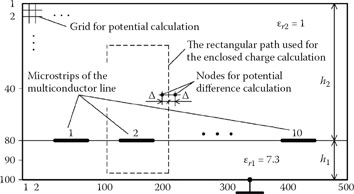
FIGURE 8.5
The cross section of the model of the microstrip multiconductor line.
According to Table 8.1, we examined four lines. Line ML1 is the microstrip multiconductor line with irregular step of conductors. Conductors of the line are identical, but gaps among them are different (s1 and s2). Lines ML2 and ML3 are considered in order to find electric parameters of the basic elements BE1 and BE2. In line ML2, the gaps between the strips are equal to s1, and the width of the strips is increased to w01 (according to Equation 8.8) in order to take into account shifts of magnetic walls (Figure 8.4). In line ML3, the gaps are equal to s2, and the widths of the strips, according to Equation (8.8), are reduced to w02. Finally, line ML4 is identical to line ML1, but the results of analysis of lines ML2 and ML3 and the developed method, based on the concept of basic elements, are used for calculation of electric parameters of line ML4.
TABLE 8.1
Relative Cross-Section Dimensions and Other Design Parameters of the Microstrip Multiconductor Line
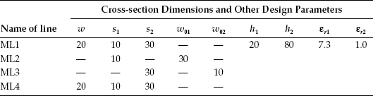

FIGURE 8.6
Equipotential lines in the cross sections of multiconductor lines ML1–ML4.
Results of the calculation of potential distribution in the central parts of microstrip multiconductor lines (in the surrounding of the conductors with order numbers from four to seven) are presented in Figure 8.6. Equipotential lines in line ML1 are shown in Figure 8.6(a). Equipotential lines in Figure 8.6(b, c) illustrate potential distributions in the multiconductor lines ML2 and ML3, containing accordingly the same basic elements BE1 and BE2. Finally, Figure 8.6(d) is composed using potential distributions in the basic elements and corresponds to the proposed model of microstrip multiconductor line ML4 with irregular step of conductors.
The pattern in Figure 8.6(d) is similar, but does not coincide with that in Figure 8.6(a). For the previous reason, calculations of distributed capacitances were performed in order to check the adequacy of the proposed model.
At known potential and electric field distributions, we can find the charge ρi on the ith conductor of unit length using the third Maxwell equation (Gauss’ law):
(8.11) |
According to Equation (8.11), we can find the charge ρi performing numerical integration along the contour lc surrounding the conductor of the multiconductor line and shown in Figure 8.5 by a dashed line:
ρi=Ql=∮lCε→E⋅→dSl=∮lCε(−∇φ)⋅→dn, |
(8.12) |
where
l is the length of the conductor
φ is potential
▽ is the nabla operator →dn=→dS/l
▽φ determines the potential gradient in the normal direction with respect to the contour lc. When the finite difference method is used, the potential gradient can be found using the following expression:
(8.13) |
where Δφ is the potential difference between the nodes that are at the distance of two mesh steps on the normal to the contour.
Consequently, in the application of the finite difference method, the charge ρi can be found by adding
(8.14) |
Then, the capacitance of the ith conductor is given by
(8.15) |
where φi is the potential of the ith conductor. In the calculations, we usually assume that φi = 1 V. Then, Ci = ρi.
TABLE 8.2
Results of Calculations of Capacitances

The results of calculations of capacitances of microstrip multiconductor line conductors are presented in Table 8.2. In this table, C(i,j)ML1 is the capacitances of the ith and jth conductors in multiconductor line ML1 at the same potentials of conductors. Values of the capacitances are identical because the multiconductor line is symmetrical. CBE1(i,j)ML2, CBE2(i,j)ML3
According to Table 8.2, values of capacitances C(4,7)MLi practically coincide with corresponding values of C(5,6)MLi, so the precision of calculations is high enough. In addition, it is very important that differences between values of the mentioned capacitances obtained for lines DM1 and DM4 are close to each other. The magnitudes of relative differences are less than 1.5%. Thus, the methodical errors of the proposed model are small and this method is suitable for calculations of capacitances of the conductors of microstrip multiconductor lines with an irregular step of conductors.
Duration of potential distribution calculations using the proposed method depends on computer capabilities, number of nodes, and number of iterations. With the application of a PC AT with Pentium IV® 1.8 GHz processor and random-access memory of 256 MB, the duration of 400 iterations is less than 7 minutes. In the analysis of basic elements, the duration of calculations is considerably less. On the other hand, calculations are very fast when analytical methods are used.
Usually, the analytical method based on conformal transformations is used [31,32]. In order to evaluate errors of calculations using the conformal transformation method and reveal the expedience of the application of this method in computer-aided design of microstrip meander delay lines, let us compare results obtained using the numerical finite difference method and the analytical method based on conformal transformations.
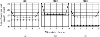
FIGURE 8.7
Distributed capacitances of conductors of multiconductor lines, (a) ML1, (b) ML2, and (e) ML3 obtained using the numerical method (curves marked by circles) and the analytical method (curves marked by triangles) at the same potentials of conductors.
In the application of the conformal transformation method, we assumed that the microstrip multiconductor lines consist of infinitely great numbers of conductors and used the software described in Martavicius and Urbanavicius [17]. The results of calculations of distributed capacitances of conductors in lines ML1, ML2, and ML3 are presented in Figure 8.7. According to this figure, errors of calculations depend on the widths of conductors, gaps among them, and the order number of the conductor. The maximal differences between calculated values of capacitances are obtained for peripheral conductors because the spread of the electric field at marginal conductors is not taken into account in the application of the analytical method.
Considering the conductors in the middle part of the lines, we see that values of capacitances obtained using the numerical and analytical methods are close to each other at wide conductors (relative differences are up to 1%). In the case of line ML1 containing wide and narrow conducting strips, the relative differences of values of capacitances are up to 8%. For narrow strips and wide gaps between them, the relative differences of values of capacitances are up to 16%. Thus, analytical and numerical methods can be used in calculations of characteristics of the microstrip multiconductor line with an irregular step of conductors. The numerical methods are undoubtedly better for seeking higher accuracy, especially when the number of conductors in the multiconductor line is limited.
8.1.2 Properties of Microstrip Meander Lines Containing Periodical Inhomogeneities
With an irregular step of conductors of the meander electrode, the meander system becomes a structure containing periodical inhomogeneities. In order to reveal properties of microstrip meander delay lines containing periodical inhomogeneities due to irregular steps of conductors, let us examine the line presented in Figure 8.8. The line consists of the meander electrode made on one side of the dielectric substrate and the metallic layer operating as a shield on the other side of the substrate. Meander systems at periodical variation of the width of conductors are investigated in Martivicius [45]. Here let us examine properties of the systems at periodical variation of the gaps among the adjacent conductors. Let us assume that the strips of the meander electrode are of the same width w, but that the gaps among the neighboring strips are different (s1 and s2). At these conditions, the step of conductors is irregular (L1≠L2). On the other hand, the step varies periodically. As a result, there are two conductors in period D of the line (D = L1 and L2).
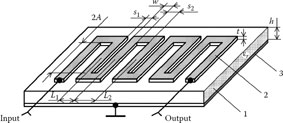
FIGURE 8.8
The structure of the meander microstrip meander line with varying step of conductors. 1: Dielectric substrate; 2: shield; 3: meander electrode.
The microstrip multiconductor line with irregular step of conductors can be used in the model of the microstrip meander delay system presented in Figure 8.8. The principles of meander system modeling and calculation of characteristics are described in references 16, 27, 33, and 37 and have also been presented in previous chapters of this book. Taking this into account, we will skip consideration of principles of simulation and will concentrate on the results of calculations.
The dispersion characteristics (in the form of the retardation factor versus frequency kR(f)) of microstrip multiconductor lines are presented in Figure 8.9. The dispersion characteristic of the meander line at a constant step of conductors is shown by the solid line (curve 1), and the characteristic at s1 ≠ s2 and L1 ≠ L2 is represented by the thin line (curve 2). Figure 8.9 illustrates that a decrease of the gap s2 is followed by an increase of the retardation factor and an increase of retardation dispersion. The increase of retardation is due to an increase of structural retardation with a decrease of s2 because the structural retardation is proportional to 4A/(L1 + L2) (A, L1 and L2 are dimensions shown in Figure 8.8). The relative increase of dispersion is greater than the relative increase of the structural retardation.
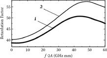
FIGURE 8.9
Retardation factor of the microstrip meander line versus frequency at εr = 7.3, w/h = 1, t/h = 0.01, S1/h = 1, A/h = 20. 1: s2/s1 = 1; 2: s2/s1 = 0.5.
Figure 8.10 shows how the retardation factor of the microstrip meander line at low-frequency kRLF depends on the ratio s2/s1. Values of the retardation factor in the plotting of each curve in Figure 8.10 are normalized with respect to the value of the retardation (according to this curve) at the same gaps (s2/s1 = 1; s2 = s1 = s).
According to Figure 8.10 (a), with a decrease of the ratio s2/s1, the retardation factor increases, obtains maximal value, and after that falls. Such a character of the dependence is determined by two factors: (1) an increase of the structural retardation with a decrease of the period of conductors, and (2) a variation of the effective dielectric permittivity in the microstrip multiconductor line, capacitances of conductors, and characteristic impedances of the conductors due to variation of the field distribution in the line. The first factor dominates with a decrease of the ratio s2/s1 from 1 to approximately 0.5; the second factor becomes the most important at lower values of s2/s1. The maximal value of the retardation factor depends on the width of conductors, thickness of the substrate, and ratio of these dimensions (w/h).
Similarly, we can explain the variation of retardation with an increase of s2/s1 in the range from 1 to 2: Retardation decreases because the structural retardation decreases. At smaller gaps between the strips of the meander electrode, the retardation factor in the low-frequency range is less dependent on the ratio s2/s1 (Figure 8.10b).
With shifts of the signal strips along the longitudinal axis of the meander electrode in opposite directions by Δs, the period of the conductors and the structural retardation factor remain constant. Dispersion characteristics of the ordinary microstrip meander line (at step of conductors L, identical gaps s1 = s2 = s) and the line at shifted meander strips (at step L and gaps s1 = s + Δs and s2 = s - Δs) are represented in Figure 8.11 by curves 1 and 2, respectively In both cases, the structural retardation kRs = 2A/L is the same—approximately 22.86. The “3” curves in Figure 8.11 are obtained at constant steps of conductors s1 = s + Δs and curve 4 at the constant step of s2 = s - Δs. Certainly, curves 1 and 2 are between curves 3 and 4 and are close to each other. Thus, small shifts of the strips of the meander electrode and change of the gaps between them (caused, for example, by technological errors) practically do not influence the retardation factor and dispersion of retardation in microstrip meander delay lines.

FIGURE 8.10
Normalized values of the retardation factor in the low-frequency range versus ratio s2/s1 at εr = 7.3, t/h = 0.01, A/h = 20. (a) s1/h = 1; (b) s1/h = 0.5. 1: w/h = 2; 2: w/h = 1; 3: w/h = 0.5.
In the general case, the input impedance of a meander system is complex and depends on coordinate x. At the center of the meander electrode (at x = 0) and at its sides (at x = ±A), the input impedance becomes real. For this reason, designers usually project terminals at the peripheral parts of the meander systems (as in Figures 8.1 and 8.8) or at the centers of the systems (at x = 0). For these reasons, let us consider on what and how the input impedances at the mentioned sections of meander electrode depend.
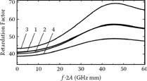
FIGURE 8.11
Retardation factor of microstrip meander lines versus frequency at εr = 7.3, w/h = 1, t/h = 0.01, A/h = 20. 1: s/h = 0.75; 2: s1/h = 1, s2/h = 0.5; 3: s/h = 0.5; 4: s/h = 1.
Frequency characteristics of input impedances of microstrip meander lines at x = 0 and x = ±A are presented in Figure 8.12. The reference curves 2 are obtained at the same widths of the gaps between the meander strips. Curves 1 and 3 characterize properties of the microstrip meander lines at narrowed and widened gaps s2, respectively.
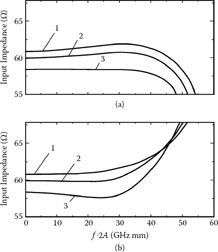
FIGURE 8.12
Input impedances of microstrip meander lines (a) at the centers of the meander strips (x = 0) and (b) at the sides of the meander electrodes (x = ±A) versus frequency at εr = 7.3, w/h = 1, t/h = 0.01, s1/h = 1, A/h = 20. 1: s2/s1, = 0.5; 2: s2/s1, = 1; 3: s2/s1, = 2.
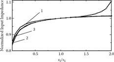
FIGURE 8.13
Dependencies of normalized input impedances of microstrip meander lines in the low-frequency range on the ratio of gap widths s2/s1 at εr = 7.3, s1/h = 1, t/h = 0.01, A/h = 20. 1: w/h = 0.5;2:w/h = l;3:w/h = 2.
At low frequencies, the input impedance of meander systems is almost the same in the sections at x = 0 and x = ±A and relatively slightly depends on frequency in the wide-frequency range. The small variation of input impedance with frequency is the valuable feature of meander systems. On the other hand, in the high-frequency range, when the phase angle θ between voltages on adjacent conductors approaches π, input impedance at the section x = 0 rapidly decreases, and at x = ±A rapidly increases.
A decrease of the gap s2 between conductors is followed by a decrease of capacitances of conductors and an increase of characteristic impedance. With an increase of s2 capacitances increase and input impedance decreases. Figure 8.13 visually illustrates how the input impedance of the microstrip multiconductor line in the low-frequency range depends on s2 at constant s1. Normalized values of the input impedance (ordinates of a curve divided by the value of the ordinate at s1 = s2 = s) are plotted along the vertical axis.
8.2 Properties of Packaged Microstrip Meander Systems
Generally, packaged microstrip meander delay lines are used [34]. The metallic package operates as the top shield of the line (Figure 8.14). Additionally, in order to increase delay time or reduce the dimensions of the delay line, sometimes dielectric plates with a metalized top surface are attached to the meander electrode at packaging [35].
The model of the microstrip multiconductor line can be found in Martavicius and Urbanavicius [36]. Using this model, the model of the packaged microstrip meander delay line has been developed and properties of the packaged delay lines examined [19]. The main results of investigation are presented in this section.
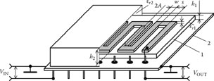
FIGURE 8.14
The structure of the packaged microstrip meander delay line. 1: Microstrip line consisting of meander conductor on dielectric substrate (with dielectric permittivity εr1) and metalized bottom side; 2: the part of the metallic package operating as the bottom and top shields of the delay line.
Two types of electromagnetic waves can propagate in meander systems [27,37]. In practice, the main wave type is used in wide-band meander delay lines. For this type, the phase angle between voltages on adjacent conductors of the meander electrode is small in the low-frequency range. At high frequencies, the phase angle usually does not exceed π/2, and the product f × 2A is less than 40 GHz.mm. Taking this into account, we will consider properties of packaged microstrip meander lines at propagation of the main type of the electromagnetic wave in the relative frequency range to 40 GHz.mm.
8.2.1 Dispersion Properties of Packaged Microstrip Meander Delay Lines
The dispersion characteristic of the microstrip meander delay line and the dispersion characteristic of this line after packaging are presented in Figure 8.15. After packaging, the electrical field in the space between the meander electrode and the top shield (in air) becomes stronger, the effective dielectric permittivity becomes less, and the delay time in the line becomes less. Also, at packaging, due to a change of distribution of the field, coupling between the strips of the meander electrode decreases. As a result, dispersion of retardation becomes less.
Figure 8.16 illustrates how the retardation factor and dispersion properties of the microstrip meander delay line depend on the distance of the top shield from the meander electrode. Asterisks in Figure 8.16 correspond to normalized frequency values 2A × fπ/2. At frequency fπ/2, the phase angle between voltages on adjacent conductors becomes equal to π/2.
In addition to Figure 8.16, information about variation of retardation approaching the top shield is presented in Table 8.3, where
(8.16) |

FIGURE 8.15
Retardation factor of the microstrip meander line versus frequency at εrl = 7.3, εr2 = 1, w/h1 = 1, s/h1 = 0.5, t/h1 = 0.01, A/h1 = 20. 1: Before packaging; 2: after packaging at h2/h1 = 1.
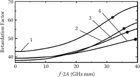
FIGURE 8.16
Retardation factor of the microstrip meander line (curve 1) and the packaged line (curves 2–4) versus frequency at εr1 = 7.3, εr2 = 1, w/h1 = 1, s/h1 = 0.5, t/h1 = 0.01, A/h1 = 20 and various distances of the top shield. 1: h2/h1 = ∞; 2: h2/h1 = 2; 3: h2/h1 = 1; 4: h2/h1 = 0.5.
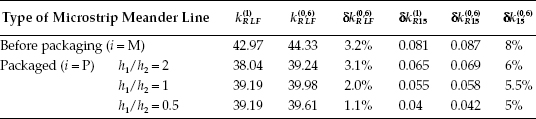
TABLE 8.3
Parametersa Characterizing Dispersion Properties of Microstrip Meander Delay Line and Packaged Line at Various Distances of Top Shield from Meander Electrode of the Line
Type of Microstrip Meander Line |
δkRLF |
δkiR15 |
r |
|
Before packaging (i = M) |
— |
— |
0.081 |
— |
Packaged (i = P) |
h2/h1 = 2 |
-0.115 |
0.065 |
1.25 |
h2/h1 = 1 |
-0.088 |
0.055 |
1.47 |
|
h2/h1 = 0.5 |
-0.088 |
0.040 |
2.03 |
|
a Parameters are found at conditions indicated in Figure 8.16.
characterizes a change of the retardation factor of the microstrip meander line in the low-frequency range,
δk(i)R15=k(i)R15−k(i)RLFk(i)RLF |
(8.17) |
indicates relative dispersion in the microstrip meander line (i = M) and the packaged line (i = P) in the frequency range from 0 f × 2A = 15 GHz mm, and shows how many times dispersion of retardation in the packaged microstrip meander delay line is less with respect to dispersion in this line before packaging.
(8.18) |
According to Figure 8.16 and Table 8.3, packaging of the microstrip meander line (using the top shield and approaching the meander electrode with it) is followed by considerable decrease of dispersion. At a small distance from the top shield (h2/h1 = 0.5), the dispersion in the relative frequency range from 0 to f × 2A = 15 GHz mm becomes more than two times less than in the unpackaged line.
Using the solid dielectric (with εr2 > 1) in the space between the meander electrode and the top shield, we can increase the effective dielectric permittivity and the delay time in the microstrip delay line. Figure 8.17 and Table 8.4 characterize the influence of the solid dielectric and the top shield on the retardation factor and dispersion properties of microstrip delay lines.
At εr2 > 1, we can obtain a retardation coefficient that is greater than the retardation in the unpackaged microstrip delay line. As a result of an increase of retardation at high frequencies, the relative frequency fπ/2 becomes less. Retardation dispersion depends on the distance of the top shield and dielectric permittivity of the material in the space between the meander electrode and the top shield. Considering data in Table 8.4, we can notice that the relative dispersion δk(i)R15
In order to reveal general properties of the packaged delay lines containing periodical inhomogeneities due to an irregular step of the meander electrode, let us assume that the width of conductors and gaps between them change periodically along the electrode:
The widths of the strips with even order numbers (2n) are w1 > w.
The widths of odd strips (2n +1) are w2 < w.

FIGURE 8.17
Retardation factors of microstrip multiconductor lines before and after packaging versus frequency at εr1 = 7.3, w/h1 = 1, s/h1 = 0.5, t/h1 = 0.01, A/h1 = 20. Various distances of the top shield—(a) h2/h1 = 1, (b) h2/h1 = 2—and various dielectric permittivities of the material in the space between the meander electrode and the top shield. 1: Unpackaged line; 2: εr2 = 1; 3: εr2 = 3.78; 4: εr2 = 7.3. Asterisks correspond to the normalized frequency values 2A × fπ/2.
TABLE 8.4
Parametersa Characterizing Dispersion Properties of Microstrip Meander Delay Line and Packaged Line at Various Distances of Top Shield from Meander Electrode of the Line and Various Dielectric Permittivities in the Space between the Meander Electrode and Top Shield

a Parameters are found at conditions indicated in Figure 8.17.
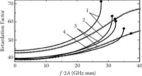
FIGURE 8.18
Retardation factors of the microstrip multiconductor line before and after packaging versus frequency with an irregular step of conductors when εrl = 73, εr2 = 1, w1/h1 = 1.25, w2/w1 = 0.6, t/h1 = 0.01, sL/h1 = 0.75, sL/sR =3, A/h1 = 20.1: Unpackaged line; 2:h2/h1 = 2; 3: h2/h1 = 1; 4: h2/h1 = 0.5. Curves at w1/h1 = w2/h1 = 1 are marked by circles. Asterisks correspond to the normalized frequency values 2A × fπ/2.
The widths of the gaps on the right sides of the even strips are sR ≠ s.
The widths of the gaps on the left sides are sL ≠ sR.
Here, w and s are dimensions of the microstrip meander line with a regular step of the meander electrode (L = w + s).
Figure 8.18 illustrates dispersion properties of the microstrip meander line with an irregular step. Parameters characterizing dispersion properties are presented in Table 8.5. The equation
δk(w2/w1)RLF=k(w2/w1)RLF−k(1)RLFk(1)RLF.100% |
(8.19) |
characterizes change of retardation in the low-frequency range due to an irregular step and
δk(w2/w1)15=δk(w2/w1)R15−δk(1)R15δk(1)R15.100% |
(8.20) |
TABLE 8.5
Parametersa Characterizing Dispersion Properties of Microstrip Meander Delay Lines with an Irregular Step of Conductors
a Parameters are found at conditions indicated in Figure 8.18.
is the relative change of dispersion in the relative frequency range from 0 to f × 2A = 15 GHz mm due to an irregular step.
In Equations (8.19) and (8.20), k(w2/w1)RLF
According to Figure 8.18 and Table 8.5, periodical inhomogeneities of the meander cause the retardation factor to increase in the low-frequency range and retardation to disperse. Periodical inhomogeneities cause essential changes of dispersion characteristics in the high-frequency range. When the phase angle between voltages on adjacent conductors approaches π/2, the retardation factor changes rapidly and the stop-band appears as in other slow-wave structures containing periodical inhomogeneities (see Section 4.3 in Chapter 4). The width of the stop-band depends on the ratio of the widths of conductors, the ratio of the gaps between them, and other factors. In Figure 8.18, only the parts of the dispersion characteristic in the frequency range to the bottom of the stop-band are presented.
8.2.3 Input Impedance of Packaged Microstrip Meander Delay Lines
The input impedance frequency characteristic of the unpackaged and packaged microstrip meander line at the middle of meander conductors and different distances of the top shield from the meander electrode are presented in Figure 8.19. In addition, information about variation of the input impedance approaching the top shield is presented in Table 8.6, where
δZINLF=Z(P)INLF−Z(M)INLFZ(M)INLF.100% |
(8.21) |
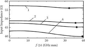
FIGURE 8.19
Input impedance of the microstrip multiconductor line before and after packaging versus frequency at εr1 = 7.3, εr2 = 1, w/h1 = 1, t/h1 = 0.01, s/h1 = 0.5, A/h1 = 20. 1: Before packaging; 2: h2/h1 = 2; 3: h2/h1 = 1; 4: h2/h1 = 0.5. Asterisks correspond to the normalized frequency values 2A.fπ/2.
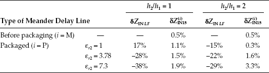
TABLE 8.6
Changes of Parametersa of Microstrip Meander Delay Line at Packaging
Type of meander delay line |
δZIN LF |
δZ(i)IN15 |
|
Before packaging (i = M) |
— |
0.5% |
|
Packaged (i = P) |
h2/h1 = 2 |
–15% |
0.3% |
h2/h1 = 1 |
–17% |
1.1% |
|
h2/h1 = 0.5 |
–25% |
1.7% |
|
a Parameters are found at conditions indicated in Figure 8.19.
is the change of the input impedance of the microstrip multiconductor line at packaging, and
δZ(i)IN15=|Z(i)IN15−Z(i)INLF|Z(i)INLF.100%, i=M,P |
(8.22) |
characterizes variation of the input impedance in the relative frequency range from 0 to f × 2A = 1.5 GHz mm.
In Equations (8.21) and (8.22), Z(i)INLF
With packaging and approaching the metallic packaging element acting as a top shield to the meander electrode, distributed capacitance of the meander electrode increases. As a result, the input impedance of the microstrip meander delay line decreases. The input impedance of the microstrip meander delay line, like input impedances of other types of meander slow-wave structures, depends only slightly on frequency. This is the valuable feature of microstrip meander lines.
Figure 8.20 and Table 8.7 characterize the influence of the solid dielectric in the space between the meander electrode and the top shield on input impedance of microstrip delay lines. The insertion of the solid dielectric causes a further increase of distributed capacitance of the meander electrode and a decrease of input impedance.
With an increase of thickness of the solid dielectric layer above the meander, the input impedance increases and becomes more dependent on frequency. The last feature is related to the surface character of the electromagnetic field. Thus, the input impedance is less dependent on frequency at a smaller thickness of the solid dielectric layer in the space between the meander electrode and the top shield. At the same time, it is important to notice that an increase of dielectric permittivity εr2 causes a decrease of relative frequency 2A × fπ/2.

FIGURE 8.20
Input impedances of microstrip multiconductor lines before and after packaging versus frequency at εrl = 7.3, w/h1 = 1, t/h1 = 0.01, s/h1 = 0.5, A/h1 = 20. Various distances of the top shield—(a) h2/h1 = 1, (b) h2/h1 = 2—and various dielectric permittivities of the material in the space between the meander electrode and the top shield. 1: Unpackaged line; 2: εr2 = 1; 3: εr2 = 3.78; 4: εr2 = 7.3. Asterisks correspond to normalized frequency values 2A × fπ/2.
TABLE 8.7
Changes of Parametersa of Microstrip Meander Delay Line at Packaging and Insertion of Solid Dielectric into Space between Meander Electrode and Top Shield
a Parameters are found at conditions indicated in Figure 8.20.
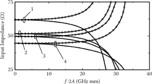
FIGURE 8.21
Input impedance frequency characteristics: Input impedances at the centers of the wide strips (solid curves) and narrow strips (lines marked by circles) of the microstrip multiconductor line before and after packaging versus frequency at an irregular step of conductors when εrl = 7.3, εr2 = 1, w1/h1 = 1.25, w2/w1 = 0.6, t/h1 = 0.01, sL/h1 = 0.75, sL/sR = 3, A/h1 = 20.1: Before packaging; 2:h2/hl=2;3,;h2/h1 = l;4: h2/h1 = 0.5.
8.2.4 Input Impedance of Packaged Microstrip Meander Delay Lines Containing Periodical Inhomogeneities
The results of calculations of characteristic impedance of microstrip meander delay lines at periodically changing steps of meander conductors are presented in Figure 8.21 and Table 8.8.
Because of the periodical variation of the step of conductors, the meander line obtains properties of a structure containing periodical inhomogeneities. The input impedance is dependent on coordinate x and the order number of conductors. Figure 8.21 illustrates how input impedance values at the centers of wide conductors (with even order numbers 2n) and narrow conductors (with odd numbers 2n + 1) depend on frequency and distance of the top shield from the meander electrode. Curves characterizing input impedance ZIN2n are represented by solid lines, and curves corresponding to ZIN(2n+1) are additionally marked by circles.
TABLE 8.8
Parametersa Characterizing Input Impedance of Microstrip Meander Delay Lines at an Irregular Step of Conductors
Type of Meander Delay Line |
δZ(0,6)INLF |
δZ(0,6)IN2n15 |
δZ(0,6)IN(2n+1)15 |
|
Before packaging (i = M) |
–7.7% |
–3.8% |
–11.6% |
|
h2/h1 = 2 |
–5.9% |
–3% |
–8.9% |
|
Packaged (i = P) |
h2/h1 = 1 |
–4.8% |
–1.9% |
–7.6% |
h2/h1 = 0.5 |
–4.2% |
–1.5% |
–7% |
|
a Parameters are found at conditions indicated in Figure 8.21.
Information about the variation of the input impedance approaching the top shield is presented in Table 8.8, where
δZ(w2/w1)INLF=Z(w2/w1)INLF−Z(1)INLFZ(1)INLF.100% |
(8.23) |
characterizes the change of the input impedance due to variation of widths of conductors, and
δZ(w2/w1)IN2n,(2n+1)15=Z(w2/w1)IN2n,(2n+1)15−Z(1)IN2n,(2n+1)15Z(1)IN2n,(2n+1)15.100% |
(8.24) |
is the relative change of the input impedance at relative frequency f × 2A = 15 GHz mm due to the variation of the widths of conductors.
In Equations (8.23) and (8.24), Z(w2/w1)INLF
According to Figure 8.21, the input impedances in the low-frequency range at the centers of wide and narrow meander strips are the same. With an increase of frequency, values of input impedances at the centers of meander strips change in opposite directions. As a result of great variation of input impedance (increase of multiple reflections in the line with periodical inhomogeneities), the microstrip multiconductor line obtains properties of the rejection filter when the normalized frequency approaches 2A × fπ/2, (i.e., when the phase angle between the adjacent conductors approaches π/2), and the length of the half-wave in the system approaches length 4A of the meander conductor in a period of the structure.
8.3 Characteristic Impedance of Meander Systems
The characteristic impedance frequency characteristic is a very important characteristic of a slow-wave structure. Matching of the structure with other elements of the signal path depends on characteristic impedance.
Researchers analyze input impedance [38,39] or characteristic impedance [40,41] of meander systems. In the application of the multiconductor line method, the usual results of calculations of input impedance are presented [39]. Unfortunately, authors use the term input impedance in the analysis of infinitively long systems and do not comment on the relationship between input impedance and characteristic impedance.
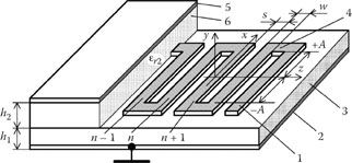
FIGURE 8.22
The structure of the microstrip meander system. 1: Meander electrode; 2: bottom shield; 3: dielectric substrate; 4: short-circuiter; 5: top shield; 6: dielectric in the space between the meander electrode and the top shield.
In this section, we will try to solve the problem related to definitions and calculation methods of input and characteristic impedances of microstrip meander delay lines (Figure 8.22) and other meander systems.
The characteristic impedance Zc of a uniform transmission line is the ratio of the amplitudes of a single pair of voltage and current waves propagating along the line in the absence of reflections [42]. Thus,
(8.25a) |
where U(jβz) and I(jβz) are complex amplitudes of voltage and current of the incident wave propagating in the direction of axis z; β is the phase coefficient of the wave.
In the application of the multiconductor line method, the infinitely long model of a slow-wave structure is usually used. Then the term input impedance is used only conditionally. The input impedance is determined as the ratio of voltage and current at some section of the conductor of the multiconductor line modeling the system:
(8.25b) |
Voltages and currents in the meander system with an inhomogeneous dielectric in its cross section are given by [45]
and
where A0 is the amplitude coefficient
kθe = kθo = k(θ + π) are wave numbers of even and odd waves in the multiconductor line modeling meander system
ϒ(θ) ϒ(θ + π) are characteristic admittances of the multiconductor line
According to Equations (8.26) and (8.27), voltages and currents are given by superposition of incident and backward waves directed by the meander electrode. The backward wave is excited due to coupling between the adjacent conductors of the meander electrode.
The incident wave propagates along even conductors (with order numbers 2n) in the direction of the x axis; components containing multiplier e-jkθex describe this wave. The expression of the incident wave propagating in the -x direction along odd conductors (with order numbers 2n ± 1) contains multiplier ejkθeX. Considering this, we can rearrange Equation (8.25) to
Substituting components of voltage (Equation 8.26) and current (Equation 8.27) describing the incident wave into Equation (8.28), we can derive the expression of the characteristic impedance of the form
(8.29) |
where
Z_IN(0)=U_n(0)I_n(0)=1√ϒ(θ)ϒ(θ + π)√sin 2kθoAsin 2kθoA |
(8.30) |
is the input impedance of the meander system at the middle of the meander conductor (at x = 0), and
K_Z(x)=1ZIN(0)ϒ(θ + π)ZIN(0)ϒ(θ + π)+e−j(kθo−kθe)xZIN(0)ϒ(θ)+e−j(kθo−kθe)x |
(8.31) |
is the ratio of characteristic and input impedances.
With a homogeneous and quasi-homogeneous dielectric in the cross section of the system, wave numbers of even and odd waves are the same (kθo = kθe). Then, Kz(x) = 1. Thus, the characteristic impedance of the meander system with a homogeneous and quasi-homogeneous dielectric in its cross section is equal to the input impedance at x = 0.
Generally, with an inhomogeneous dielectric, the characteristic impedance of the meander system is complex and dependent on coordinate x and frequency. At the centers of conductors, the characteristic impedance Zc(0) is real, but different from input impedance ZIN(0). The ratio of these impedances is given by
K_Z(0)=1ZIN(0)ϒ(θ + π)1+ZIN(0)ϒ(θ + π)1+ZIN(0)ϒ(θ). |
(8.32) |
At x = ±A, according to calculations, imaginary parts of characteristic and input impedances are small. The maximal phase angle of the phasor Kz is less than 0.01 π.
Figure 8.23 characterizes how absolute values of characteristic and input impedances of the microstrip meander line at the center of meander conductors and at the sides of the meander electrode and the absolute value of the ratio of characteristic and input impedances depend on frequency.
According to Equations (8.29)–((8.32)), the characteristic impedance of the meander line with a nonhomogeneous dielectric in its cross section in the low-frequency range is active and independent on coordinate. Values of characteristic and input impedance are close to each other. Ratio Kz is given by
K_ZLF=(1+√ϒ(0)ϒ(π)4√εref(0)εref(π))/(1+√ϒ(0)ϒ(π)4√εref(π)εref(0)), |
(8.33) |
where ϒ(0), ϒ(π), εr ef(0), and εr ef(π) are characteristic impedances and effective dielectric permittivities of the multiconductor line used in the model of the microstrip meander line at phase angles between voltages on neighboring conductors equal to 0 and π.
Coefficient KZLF is dependent on effective dielectric permittivities. According to Figure 8.23, at εr ef(0) > εr ef(π), characteristic impedance at low frequency is higher than input impedance; at εr ef(0) < εr ef(π), it is less than input impedance. The magnitude of differences between values of characteristic and input impedances is less than 5%.

FIGURE 8.23
Characteristic (solid lines) and input (thin lines) impedances of the microstrip meander line (a) at the centers, (b) at the sides of meander electrode, and (c) ratio of these impedances (at x = 0 and x = A) versus frequency at εrl = 7.3, εr2 = 1, w/h1 = 1.25, w2/w1 = 0.6, t/h1 = 0.01, s/h1 = 0.75, sK/ sD = 3,A/h1 = 20.1:h2/h1=2;2:h2/h1 = 0.5.
With an increase of frequency fπ/2, characteristic and input impedances slightly decrease and approach each other. At frequency fπ/2, characteristic and input impedances obtain the same values:
(8.34) |
A further increase of frequency (in the range from fπ/2 to fπ is followed by an increase of characteristic impedance at εr ef(0) > εr ef(π) to
(8.35) |
and a decrease of characteristic impedance at εr ef(0) < εr ef(π) to
(8.36) |
The ratio Kz changes rapidly in the frequency range from fπ/2 to fπ, approaching infinity at εr ef(0) > εr ef(π) and 0 at εr ef(0) < εr ef(π).
According to analysis, characteristic impedances of meander systems with a homogeneous dielectric are equal to input impedance ZIN(0). With an inhomogeneous dielectric in the cross section, values of characteristic impedance at frequencies to fπ/2 are close to values of input impedance ZIN(0) (Figure 8.23c). Thus, the input impedance at the middle of meander conductors can be used as the parameter characterizing meander systems in analysis and design.