
CONTENTS
14.3.2 Probe Height Control System
14.3.3.1 Calibration of Resolution
14.3.3.2 Elimination of Optical False Images
14.4.1 Simulation Based on FDTD Method
14.4.2 Measurement of the Profile of Micro-Focused Spot
14.4.3 Super-Resolution Imaging
Looking back, over the past 500 years, the resolution of the optical microscope was not improved in an order of magnitude after its invention because of the diffraction limit.
In order to break through such limit, in 1928, E.H. Synge published a paper in Philosophical Magazine titled “A suggested method for extending microscopic resolution into the ultra-microscopic region.” He proposed a new idea of microscope that could possibly achieve a resolution within 0.01 μm. However, the technology then available of mechanical precision and the intensity of light source was not advanced enough to satisfy the requirements for the new-type microscope. As a result, his paper was easily forgotten until the invention of the scanning near-field optical microscope (SNOM).
In the beginning of 1980s, Dr. G. Binnig and H. Rohrer in IBM Research Center of Zurich, Switzerland, solved the problem of controlling probe scanning on the sample surface within the nanometer scale, and the first scanning tunneling microscope (STM) was invented [1], winning them a Nobel Prize in 1986. In 1984, Dr. D.H. Pohl in the same research center applied this technology to control the optical probe, and the first SNOM was born [2]. Since then great progress, both theoretical and technological, has been made. The advantages of SNOMs are high resolution, non-invasive nature for various materials, and unique optical spectral information. These make SNOMs a strong and versatile member in the scanning probe microscope (SPM) family, and they are widely used in micro/nano-science and technology fields.
In this chapter, key aspects of near-field optics including fundamental principles, novel methods, instrumental technologies, and applications in nanofabrication and nanomeasurement fields are introduced.
It is well known that when light irradiates from an optically denser medium (medium 1) into one that is optically less dense (medium 2) with an angle θ1 larger than the critical angle θc, a total reflection occurs. Nevertheless, the electromagnetic field does not disappear in medium 2 and its electric vector can be written as [3]
where
n1 and n2 are the index of refraction of medium 1 and 2, respectively
n = n1/n2 is the relative index of refraction
ω is the angular frequency
k2 = 2π/λ2 is the wave number
λ2 is the wavelength in medium 2
Equation 14.1 implies that there exists a kind of surface wave on the boundary between mediums 1 and 2, namely evanescent wave. It is a kind of inhomogeneous wave along the surface x and its amplitude along z attenuates exponentially. Actually, according to the boundary conditions of electromagnetic field, evanescent wave exists with necessity because electric and magnetic fields cannot discontinue on the surface between two mediums.
Evanescent wave does not only exist in the boundary where the total reflection occurs. When studying the reflection and transmission of a finite object, a formula similar to Equation 14.1 can be obtained using the Fourier analysis method, that is, an evanescent wave attenuates sharply along Z direction. The finite objects generate propagating and evanescent waves at the same time. The propagating waves are the radiation components, while the evanescent waves are non-radiation components. Because radiation components only contain the low-frequency part of spatial frequency, to improve the signal bandwidth of the optical detection system, that is, to improve the optical resolution, non-radiation field components have to be collected. In other words, only by collecting the high spatial-frequency information carried by the evanescent field can the high-resolution that breaks the diffraction limit be obtained [4].
The properties of evanescent field are as follows:
1. Evanescent field only exits within a scale of wavelength. This implies we could only use evanescent field to detect the ultraprecise structures.
2. Evanescent field is a spatial exponential-decay field in a scale of wavelength, which indicates that its application should be limited to a very small spatial range.
3. None of the evanescent fields transfer energy outside, so they are non-radiation fields. However instant energy flux do exist.
Usually, the SNOM consists of several parts such as laser, optical probe, three-dimensional scanner, probe height control system, optoelectric accepter, and the computer (Figure 14.1). There are several work modes as shown in Figure 14.2. The most common one is the transmission mode, which can be divided into the illumination mode (Figure 14.2a) and the collection mode (Figure 14.2b). However, when the object is opaque, the reflection mode (Figure 14.2c) is necessary.
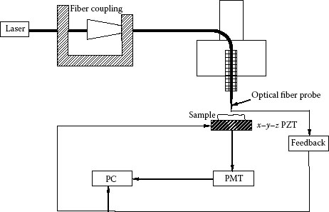
FIGURE 14.1 Schematic diagram of the structure of the near-field optical microscope system.
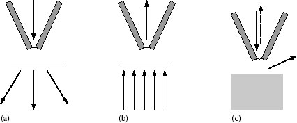
FIGURE 14.2 Work modes of the near-field optical microscope: (a) illumination mode, (b) collection mode, and (c) reflection mode.
In SNOM, the core element is the optical probe with a pinhole, which is used to illuminate the sample at the nanometer scale with its aperture smaller than the wavelength. This aperture determines the upper limit of resolution of the near-field optical microscope. The optical probes are divided into two kinds: optical fiber probe (with pinhole) and apertureless probe.
There are two methods to make the optical fiber probe: heat stretching and chemical etching methods. In the heat stretching method, a carbon dioxide laser is used to heat the fiber; meanwhile, force is applied to stretch the fiber till its abruption, and then two conically shaped probes can easily be obtained (Figure 14.3). While in the chemical etching method, fiber is put into hydrofluoric acid to get etched (Figure 14.4). The diameter of the pinhole on the tip of the fiber is usually tens of nanometers. Sometimes, a metallic film can be coated on the surface of the probe to get better optical signals.
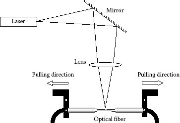
FIGURE 14.3 Schematic diagram of the heating stretching method.
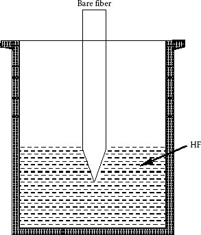
FIGURE 14.4 Schematic diagram of the chemical etching method.
The structure of the typical optical fiber probe is shown in Figure 14.5. The apex of the probe is the detection part, which can be made in nano-order, with the diameter d = 2a conducting electromagnetic exchanges with sample. The tapered part is simply a cone, whose apex angle is θ. The outside of the probe is covered by the opaque metallic file to avoid the disturbance of external light [5].
However, the commercial SNOM probes of high resolution (<50 nm) are usually very expensive. The probe fabrication, particularly with high-resolution aperture, high reproduction, and low cost, is of great interest to users of SNOM.
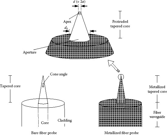
FIGURE 14.5 Schematic diagram of the typical shape of the probe. (From Ohtsu, M. (Ed.), Near-Field Nano/Atom Optics and Technology, Springer, Berlin, Germany, 1998. With permission.)
Figure 14.6 shows the side view (left) and back view (right) of the probe on a cantilever structure, respectively [6]. This kind of aperture is manufactured by focused ion beam. The bottom part is removed to allow light to transmit through the pinhole. The size of the pinhole can be precisely controlled (120–40 nm) if well designed, to get ideal resolution capability. The optical efficiency passing through the aperture is higher than through the conic fiber.
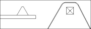
FIGURE 14.6 Structure image of a SNOM aperture.
Another kind of probe is called the apertureless probe. Usually, the probe of atomic force microscope (AFM) with a metal-coated tip is used. The aperture on the AFM tip is much sharper than that on optical fiber. When a laser irradiates onto the metal probe of AFM, the local light field will be enhanced under the probe. The enhancement can reach more than 100 times. So this novel method is especially used in nanofabrication. As shown in Figure 14.7a, when polarized light irradiates onto the surface of the probe, the distribution of electron charges will vary with the polarized directions. Figure 14.7b shows the energy distribution when incident light is P-polarized [7].
14.3.2 PROBE HEIGHT CONTROL SYSTEM
In order to bring the probe to the near-field area to control the distance between probe and sample stably with nanometer sensitivity, probe height detection and control methods must be adopted. Among these, the most widely used one is the so-called shear force method.
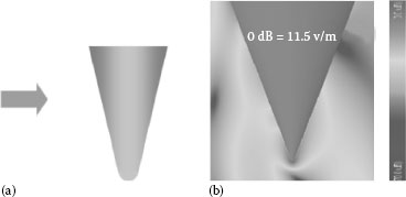
FIGURE 14.7 Schematic diagram of an apertureless probe and distribution of transient electric field. (a) Schematic diagram of an apertureless probe and (b) distribution of transient electric field.
When the probe moves close to the sample surface in several tens of nanometers, vibrating with the frequency of mechanical resonance parallel to the surface, lateral shear force will generate from the interaction between the probe and the sample. Therefore, the vibration will be attenuated due to the damping of the shear force. Thus, the amplitude of vibration can reflect the distance value between the probe and the sample. By introducing the feedback system to control the amplitude, the probe height control can be achieved. The methods for detecting the vibration of the probe can mainly be divided into two types: optical methods and non-optical methods.
In optical methods, another light source is adopted to detect the amplitude and phase of the probe vibration to control the distance between the probe and the sample. However, since the intensity of the detecting light is stronger than in the optical probe, it will cause great disturbance to the nearfield signal. Now, non-optical methods are more widely adopted in SNOM. For instance, fixing an optical fiber probe on one leg of the quartz tuning fork, and the other leg glued on a piezoelectric ceramic tube. Applying voltage can make the tuning fork vibrate with its resonance frequency parallel to the sample surface. The distance variation between the probe and the sample will cause a change in the amplitude of the tuning fork. As a result, the distance between the probe and the sample can be controlled.
To avoid the short comings of the tuning fork’s fragility and difficulty in assembling, in 1996, J. Barenz proposed that optical fiber can be inserted into minute piezoelectric ceramics divided into four split electrodes [8]. When the driving signal is applied on one quadrant, the vibration signal obtained from the other three can be used to detect shear force. However, it is hard to detect the small harmonic peak under the background of huge vibration peaks. In order to detect such harmonic peaks, a novel structure of exciting film-foil detector-probe can be used (Figure 14.8), where two pieces of piezoelectric ceramics are introduced, the thicker one for excitation, while the thinner one with optical fiber probe attached for detecting the vibration of the probe. When resonance happens, higher voltage output can be obtained [9].
14.3.3.1 Calibration of Resolution
SNOM is widely used because of its super spatial resolution. It is a great task to evaluate the resolution qualitatively. Now people usually use some methods adopted for calibrating high-resolution optical microscopes. For instance, high-resolution one- or two-dimensional diffraction grating, for which micro-fluorescent balls can be used. Recently, a work group was set up for “Standards on the definition and calibration of spatial resolution of NSOM/SNOM” in ISO/TC201/SC9. This proposal is now under discussion, and it will be standardized in about 2 years.
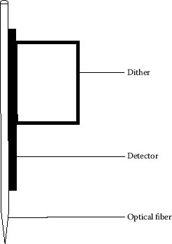
FIGURE 14.8 A kind of experiment scheme for shear force control. (From Wang, K. et al., J. Chin. Elect. Microsc. Soc., 18, 124, 1999. With permission.)
14.3.3.2 Elimination of Optical False Images
Generally speaking, the image obtained from a SNOM carries a lot of information. In other words, there are many parameters that will affect the final SNOM image, such as the optical properties of the sample, the geometric structure of the sample, the scanning parameters, the surrounding environmental conditions, etc. This means we must abstract useful information from the raw data. An interesting example can be found from Ref. [10]. In the simulation, the image shows a valley position, but it corresponds to the assumed peak position. After reconstruction, the image will be more close to the original structure. A brief introduction to this reconstruction is as follows.
Supposing that the surface equation of the contact surface is z = f(x, y), which can be written in Fourier form as follows:
By introducing the boundary conditions, we get a coupled algebraic equation that can be solved by iteration. It is known that
where
U(x, y) stands for the detected signal where the probe tip is located
H(x, y) is the convolution function of the detection apparatus
I(x, y) is the near-field intensity, which is proportional to |E|2
E is the amplitude of electric vector
and
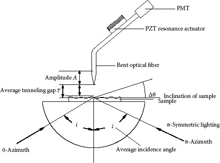
FIGURE 14.9 Schematic diagram of the instrumentation of AF/PSTM. (From Wu, S. et al., Proc. SPIE, 4923, 21, 2002. With permission.)
where F and F–1 stand for Fourier transformation and its inverse transform, respectively. After calculation, the final form of the equation is
Furthermore, hardware can also be used to eliminate optical false images. Professor S.F. Wu proposed a method of illuminating by π-symmetry dual-beam [11]. And the invention of atomic force/photon scanning tunneling microscope (AF/PSTM) is used to obtain two images of AFM (topography and phase image) and another two optical ones (transmitting efficiency and refractive index image), which can eliminate the optical false image effectively. Figure 14.9 shows the scheme of the instrumentation of AF/PSTM; when incident light irradiates from 0-direction and π-direction simultaneously, optical false image can be eliminated.
14.4.1 SIMULATION BASED ON FDTD METHOD
The algorithm of finite-difference time-domain (FDTD) method proposed by K.S. Yee in 1996, is simply a mathematical method solving Maxwell equations related to the time domain deduced from the finite element method. The FDTD method makes discretization of the Maxwell equation both in the time domain and the spatial domain to substitute the original differential equation with a finite difference scheme.
FIGURE 14.10 Schematic diagram of the experimental setup for measurement of the intensity distribution at the focus. (From Fu, Y.H. et al., J. Microsc., 210, 225, 2003. With permission.)
The FDTD method can directly deal with the Maxwell equations avoiding the extra use of mathematical tools. Therefore, the FDTD method is widely used in the simulation of near-field optics. For example, using the FDTD method to simulate the light propagation in an optical fiber probe with aperture, the relationship between the spatial resolution and the collecting efficiency of the aperture diameter can be obtained [12].
14.4.2 MEASUREMENT OF THE PROFILE OF MICRO-FOCUSED SPOT
Near-field optics can also be used to measure the profile of focused laser spots, which is difficult to do by traditional optical method. Y.H. Fu et al. introduced their experimental setup for measuring the intensity distribution of a micro-spot [13]. An object lens with a high numerical aperture (NA) was used to focus the incident light, and a tapered probe of the SNOM system (Figure 14.10) was used to detect the intensity of the focal field. The measured spatial resolution was determined by the size of the near-field optical fiber probe (usually, <100 nm).
The results show an asymmetric distribution of the focused intensity with the linear-polarized laser beam due to the aberration effects of the focusing lens, which means that polarization and aberration play important roles in the focusing of a high-NA lens.
14.4.3 SUPER-RESOLUTION IMAGING
SNOM is famous for its high-resolution power to break through the diffraction limit. However, its weakness is also obvious, due to its fragility and low transmitting efficiency. To avoid these problems, SNOM can be combined with the conventional confocal laser scanning microscope (CLSM) to achieve super resolution [14]. It can be switched between SNOM mode and CLSM mode easily and rapidly, which makes the detection efficiency high enough to investigate a single fluorochrome for it can be applied to biomedical field. The resolution of 300 nm can be reached with this kind of scanning confocal microscope. Figure 14.11 shows the scheme of a SNOM/CLSM.
FIGURE 14.11 Schematic diagram of the SNOM/CLSM system. (From Freyland, J.M. et al., Microelectron. Eng., 53, 653, 2000. With permission.)
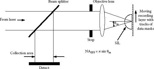
FIGURE 14.12 Schematic diagram of a kind of solid immersion lens (SIL) system. (From Milster, T.D. et al., Jpn. J. Appl. Phys., 40, 1778, 2001. With permission.)
In order to solve the problems caused by conventional probes, the virtual probe concept, which is based on the principle of evanescent wave interference, was introduced into near field [15,16,17]. It has been demonstrated by simulation that the transmitting efficiency of virtual probes is about 10 times higher than that of conventional probes; its effective working distance is about 10 times longer than that of conventional probes; and the full width at half maximum (FWHM) of the central peak of the virtual probe remains constant over a certain range. The virtual probe can be used in optical storage, nanolithography, near-field imaging, near-field measurement, etc. Figure 14.12 shows an application example of the virtual probe in SIL near-field recording [18].
In the information industry, “smaller, faster, and cheaper” is pursued. Miniaturization is the most important driving force. With the progress of micro-nanotechnology, lithography at nanometer scale resolution is required. Nanolithography is an essential basis for microelectronic-integrated manufacturing and micro-electro-mechanical system (MEMS), containing all kinds of nontraditional processing and high-energy beam processing.
At the end of the last century, a nanolithography method of near-field-enhanced laser based on the theory of SPM was developed. A laser beam irradiating onto the SPM tip surface, locally enhanced optical field will be generated beneath the probe, to do the processing on sample [7,19,20]. Heat expansion shows little influence on the femtosecond laser processing based on AFM, while the effects on the surface of the sample are mainly caused by the interaction between the locally enhanced optical field and the sample, which will not scratch the surface mechanically. Figure 14.13 shows a series of lines obtained when pulse energy is 6 nJ, and the scanning speed is 0.2 μm/s, with FWHM less than 100 nm and height of lines about 4 nm. All the processing will be done within 3 min. An increase in energy density of manufacturing will increase the height and width of poly (methyl methacrylate) (PMMA) lines.
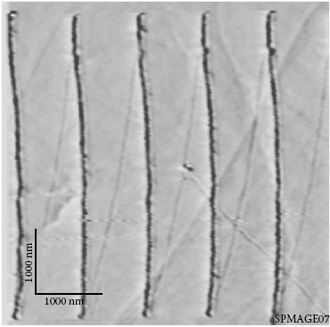
FIGURE 14.13 Nanofabricated lines on PMMA by femtosecond laser processing.
Recently, a new approach has been developed for nanolithography using nanoaperture. The FTDF method can be introduced for analyzing the excitation of surface plasmon, and designing nanoaperture with the shape of H (Figure 14.14) to gain the resolution at nano-order for nanolithography.
FIGURE 14.14 Schematic diagram of nanoaperture with the H-shape aperture.
Nowadays, the optical method and magneto-optical (MO) method cannot achieve higher storage density on account of the diffraction limit. Since 1992, when E. Betzig first realized the storage of MO method in near field [21], a lot of contributions have been made to increase the density of storage.
In 1996, B.D. Terris et al. applied SIL to the technology of near-field storage [22]. They obtained a spot with the size of 317 nm, by using a SIL in glass whose refractive index is 1.83 illuminated by the light (λ= 780 nm). Figure 14.15 shows the device used in the experiment. It was proved to be possible to achieve 125 nm spots and the storage densities approaching 40 Gb/in.2 with shorter wavelength light.
Then, phase-change recording layers based on conductive AFM were developed [23]. The method has provided an opportunity for studying the recorded marks on phase-change rewriteable optical disks in depth, especially for marks on super-resolution near-field structure disks. Moreover, using this method, recording marks within 100 nm has been achieved.
The problem of the storage of high spatial resolution has been settled; however, difficulties still exist in the control of distance between the probe and the medium less than a wavelength, and the rapid speed of scanning. As we know, the speed of near-field recording is in the order of micrometers per second, while that of digital video disk (DVD) is higher than 3.5 m/s.
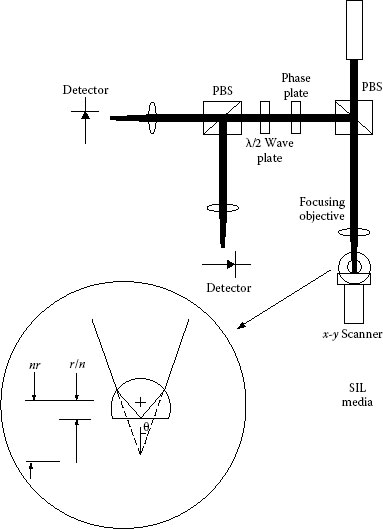
FIGURE 14.15 Schematic diagram of the optical storage test setup with the SIL device. (From Terris, B.D. et al., Appl. Phys. Lett., 65, 388, 1994. With permission.)
Besides, SNOM is also widely used to study the spectroscopy of a single molecule in biomedical field [24], or used to obtain both the morphology and optical properties of the photonic crystals (PCs) simultaneously in the field of metrology [25].
In summary, near-field optics plays an active and important role in nanofabrication and nanometrology fields. It will have a brighter future with the development of novel methods and technologies, especially those for high spatial resolution, high scanning speed, and for parallel and mass production.
1. G. Binning, H. Rohrer, C. Gerber et al. 1982. Surface studies by scanning tunneling microscopy. Physical Review Letters 49: 57–61.
2. D. W. Pohl, W. Donk, and M. Lanz. 1984. Resolution of internal total reflection scanning near-field optical microscopy. Applied Physics Letters 44: 651–653.
3. M. Ohtsu and K. Kobayashi. 2003. Optical Near Field: Introduction to Classical and Quantum Theories of Electromagnetic Phenomena at the Nanoscale. Berlin, Germany: Springer.
4. D. Courjon, J.-M. Vigoureux, M. Spajer, K. Sarayeddine, and S. Leblanc. 1990. External and internal reflection near field microscopy: Experiments and results. Applied Optics 29: 3734–3740.
5. M. Ohtsu (Ed.). 1998. Near-Field Nano/Atom Optics and Technology. Berlin, Germany: Springer.
6. E. Jin and X. Xu. 2008. Focussed ion beam machined cantilever aperture probes for near-field optical imaging. Journal of Microscopy 229: 503–511.
7. L. Zhu, F. Yan, Y. Chen et al. 2007. Femto-second laser induced nano structuring on PMMA. In Sixth Asia-Pacific Conference on Near-Field Optics, Yellow Mountain, China.
8. J. Barenz, O. Hollricher, and O. Marti. 1996. An easy-to-use non-optical shear-force distance control for near-field optical microscopes. Review of Scientific Instruments 67: 1912.
9. K. Wang, X. Wang, N. Jin et al. 1999. The study of the height regulation technique of SNOM optical probe tip (in Chinese). Journal of Chinese Electron Microscopy Society 18: 124–128.
10. Z. Jin, W. Yi, and W. Huang. 1998. Reconstruction of the surface topography by detected SNOM/PSTM signals. Applied Physics A 66: 915–917.
11. S. Wu, J. Zhang, Y. Li et al. 2002. The development of AF/PSTM. Proceedings of SPIE 4923: 21–25.
12. H. Nakamura, T. Saiki, H. Kambe et al. 2001. FDTD simulation of tapered structure of near-field fiber probe. Computer Physics Communication 142: 464–467.
13. Y. H. Fu, F. H. Ho, W. C. Lin et al. 2003. Study of the focused laser spots generated by various polarized laser beam conditions. Journal of Microscopy 210: 225–228.
14. J. M. Freyland, R. Eckert, and H. Heinzelmann. 2000. High resolution and high sensitivity near-field optical microscope. Microelectronic Engineering 53: 653–656.
15. T. Hong, J. Wang, L. Sun et al. 2002. Numerical simulation analysis of a near-field optical virtual probe. Applied Physics Letters 81: 3452–3454.
16. T. Hong, J. Wang, L. Sun et al. 2004. Numerical and experimental research on the near-field optical virtual probe. Scanning 26: 1–6.
17. Q. Sun, J. Wang, T. Hong et al. 2002. A virtual optical probe based on evanescent wave interference. Chinese Physics 11: 1022–1027.
18. T. D. Milster, F. Akhavan, M. Bailey et al. 2001. Super-resolution by combination of a solid immersion lens and an aperture. Japanese Journal of Applied Physics 40: 1778–1782.
19. E. Jin and X. Xu. 2005. Obtaining super resolution light spot using surface plasmon assisted sharp ridge nanoaperture. Applied Physics Letters 86: 111106.
20. E. Jin and X. Xu. 2006. Enhanced optical near field from a bowtie aperture. Applied Physics Letters 88: 153110.
21. E. Betzig, J. K. Trautman, R. Wolfe et al. 1992. Near-field magneto-optics and high density data storage. Applied Physics Letters 61: 142.
22. B. D. Terris, H. J. Mamin, and D. Rugar. 1994. Near-field optical data storage using a solid immersion lens. Applied Physics Letters 65: 388–390.
23. S. K. Lin, I. C. Lin, S. Y. Chen et al. 2007. Study of nanoscale recorded marks on phase-change recording layers and the interactions with surroundings. IEEE Transactions on Magnetics 43: 861–863.
24. M. Nirmal, B. O. Dabbousi, M. G. Bawendi et al. 1996. Fluorescence intermittency in single cadmium selenide nanocrystals. Nature 383: 802–804.
25. B. Jia, J. Li, and M. Gu. 2006. Near-field characterization of three-dimensional woodpile photonic crystals fabricated with two-photon polymerization. In 90th USA Annual Meeting, Rochester, NY.