
CONTENTS
25.1 Introduction to Basic Concepts
25.1.1 Stokes Parameters, Stokes Vector, and Light Polarization
25.1.2 Mueller Matrices and Optical Devices
25.1.3 Retardation and Diattenuation
25.2.1 Early PEM-Based Stokes Polarimeters in Astronomy
25.2.2 Imaging Stokes Polarimeters Using the PEM
25.2.3 Laboratory Dual PEM Stokes Polarimeters
25.2.4 Dual PEM Stokes Polarimeter Used in the Tokamak
25.2.5 Commercial Dual PEM Stokes Polarimeters
25.2.5.1 Visible Stokes Polarimeters
25.2.5.2 Near-Infrared Fiber Stokes Polarimeters
25.2.5.3 Spectroscopic Stokes Polarimeter
25.3 Mueller Matrix Polarimeter
25.3.1 Dual PEM Mueller Matrix Polarimeter
25.3.2 Four Modulator Mueller Polarimeter
25.4.1 Linear Birefringence Polarimeters and Their Applications in the Optical Lithography Industry
25.4.1.1 Linear Birefringence Polarimeter
25.4.1.2 Linear Birefringence in Photomasks
25.4.1.3 Effect on Image Quality Due to Linear Birefringence in a
25.4.1.4 Deep Ultraviolet Linear Birefringence Polarimeter
25.4.1.5 Measuring Linear Birefringence at Different DUV Wavelengths
25.4.1.6 DUV Polarimeter for Measuring Lenses
25.4.2 Near-Normal Reflection Dual PEM Polarimeter and Applications Nuclear Fuel Industry
25.4.3 Special Polarimeters for the FPD Industry
25.4.3.1 Measuring Glass Substrate
25.4.3.2 Measuring LCD-FPD Components at RGB Wavelengths
25.4.3.3 Measuring Retardation Compensation Films at Normal and Oblique Angles
25.4.3.4 Measuring Retardation at a Fast Speed
25.4.4 Special Polarimeters for Chemical, Biochemical, and Pharmaceutical Applications
25.4.4.1 Circular Dichroism Spectrometer
25.4.4.2 Optical Rotation Polarimeter
25.4.4.3 Polarization Analyzer for Fluorescence and Scattering
25.4.5 Stress Birefringence Polarimeter for Si Used in the Solar Photovoltaic Industry
25.4.6 PEM—Camera Imaging Polarimeter
A dictionary definition of polarimetry is “the art or process of measuring the polarization of light” [1]. A more scientific definition is that polarimetry is the science of measuring the polarization state of a light beam and the diattenuating, retarding, and depolarizing properties of materials [2]. Similarly, a polarimeter is an optical instrument for determining the polarization state of a light beam, or the polarization-altering properties of a sample [2].
There are several ways to categorize polarimeters. By definition [2], polarimeters can be broadly categorized as either light-measuring polarimeters or sample-measuring polarimeters. A light-measuring polarimeter is also known as a Stokes polarimeter, which measures the polarization state of a light beam in terms of the Stokes parameters. A Stokes polarimeter is typically used to measure the polarization properties of a light source. A sample-measuring polarimeter is also known as a Mueller polarimeter, which measures the complete set or a subset of polarization-altering properties of a sample. A sample-measuring polarimeter is used to measure the properties of a sample in terms of diattenuation, retardation, and depolarization. There are functional overlaps between light-measuring and sample-measuring polarimeters. For example, one can direct a light beam with known polarization properties onto a sample and then use a Stokes polarimeter to study the polarization-altering properties of the sample.
Polarimeters can also be categorized by whether they measure the complete set of polarization properties. If a Stokes polarimeter measures all four Stokes parameters, it is called a complete Stokes polarimeter, or an incomplete or a special Stokes polarimeter. Similarly, there are complete and incomplete Mueller polarimeters. Nearly all sample-measuring polarimeters are incomplete or special polarimeters, particularly for industrial applications. These special polarimeters bear different names. For example, a circular dichroism (CD) spectrometer, which measures the differential absorption between left and right circularly polarized light (Δ A = AL − AR), is a special polarimeter for measuring the circular diattenuation of a sample; a linear birefringence measurement system is a special polarimeter for measuring the linear retardation of a sample.
Another way to classify polarimeters is by how the primary light beam is divided. The primary light beam can be divided into several secondary beams by beam splitters and then each secondary beam can be sent to an analyzer–detector assembly (amplitude division) for the measurement of its polarization properties. The primary light beam can be partitioned by apertures in front of an analyzer–detector assembly (aperture division) so that different polarization properties can be measured from different parts of the primary beam. The primary light beam can also be modulated by polarization modulators, and different polarization properties are then determined from different frequencies or harmonics of the modulators.
Polarimeters have a great range of applications in both academic research and industrial metrology. Polarimeters are applied to chemistry, biology, physics, astronomy, material science, and many other scientific areas. Polarimeters are used as metrology tools in the semiconductor, fiber telecommunication, flat panel display (FPD), pharmaceutical, and many other industries. Different branches of polarimetry have established their own scientific communities, within which regular conferences are held [3,4,5,6,7]. Tens of thousands of articles have been published on polarimeters and their applications, including books and many review articles [2,8,9,10,11,12,13,14,15,16]. It is beyond the scope of this chapter to review the full range of polarimetry. Instead, I will introduce necessary general concepts for polarimetry and focus on polarization modulation polarimeters using the photoelastic modulator (PEM) [17,18].
25.1 INTRODUCTION TO BASIC CONCEPTS
25.1.1 STOKES PARAMETERS, STOKES VECTOR, AND LIGHT POLARIZATION
The polarization state of a light beam can be represented by four parameters that are called the Stokes parameters [19,20,21,22]. There are two commonly used notations for the Stokes parameters, (I, Q, U, and V) [20] and (S0, S1, S2, and S3) [8,9]. However, Shurcliff, in his polarization book [22], used the (I, M, C, and S) notation. I will use the (I, Q, U, and V) notation in this chapter.
The four Stokes parameters are defined as follows:
• I ≡ total intensity
• Q ≡ I0 – I90 = difference in intensities between horizontal and vertical linearly polarized components
• U ≡ I+45 – I−45 = difference in intensities between linearly polarized components oriented at +45° and −45°
• V ≡ Ircp – Ilcp = difference in intensities between right and left circularly polarized components
The four Stokes parameters can be grouped in a column to form a Stokes vector. The Stokes vector can represent both completely polarized light and partially polarized light. If the light beam is completely polarized,
If the light beam is partially polarized,
The degree of polarization (DOP) of a light beam is
In addition to the Stokes vector, the Jones vector [23] and Poincare sphere [20,21] are other commonly used methods to represent light polarization. I will only use the Stokes vector in this chapter.
25.1.2 MUELLER MATRICES AND OPTICAL DEVICES
When the Stokes vector is used to represent the polarization state of a light beam, the Mueller matrix [24] is typically used to represent an optical device (such as a linear polarizer, a quarter-wave plate, an elliptical retarder, etc.) and to describe how it changes the polarization state of a light beam. A Mueller matrix is a 4 × 4 matrix that is defined as follows:
where
I, Q, U, and V are the Stokes parameters of the light beam entering the optical device
I′, Q′, U′, and V′ are the Stokes parameters of the light beam exiting the optical device
The derivations and tabulated Mueller matrices for optical devices commonly used in polarization optics are available [2,8,9,10,20,21,22,25]. For example, the Mueller matrix of a general linear retarder with the linear retardation of δ and the angle of fast axis of ρ is
The Mueller matrix of a general linear retarder can be simplified to more specific cases. For instance, when δ = π/2 and ρ = 0, the Mueller matrix becomes
that represents a quarter-wave plate with its fast axis oriented at 0°.
Notice that most available Mueller matrices are derived for ideal optical elements. For example, the aforementioned Mueller matrix represents an ideal linear retarder. This Mueller matrix contains no diattenuation, which is evident from the null values of the matrix elements in the first row and the first column except m11.
25.1.3 RETARDATION AND DIATTENUATION
Polarization-altering properties of a sample include diattenuation, retardation, and depolarization. Depolarization, referring to changing polarized light to unpolarized light, is perhaps the least understood. My favorite definition of unpolarized light is that “light is unpolarized only if we are unable to find out whether the light is polarized or not [26].” One may say the definition of unpolarized light is “less scientific.” Furthermore, all the applications described in this chapter have negligible depolarization. I will only introduce retardation and diattenuation.
Linear birefringence is the difference in the refractive indices for two orthogonal components of linearly polarized light. The linear birefringence of an optical element produces a relative phase shift between the two linear polarization components of a passing light beam. The net phase shift integrated along the path of the light beam through the optical element is called linear retardation or linear retardance. Linear retardation requires the specification of both magnitude and angle of fast axis. The fast axis corresponds to the linear polarization direction for which the speed of light is a maximum (or for which the refractive index is a minimum). Linear birefringence, linear retardation, and linear retardance are sometimes loosely used interchangeably.
Circular birefringence is the difference in the refractive indices for right and left circularly polarized light. The circular birefringence of a sample produces a relative phase shift between the right and left circularly polarized components of a passing light beam. The net phase shift integrated along the path of the light beam through the sample is called circular retardation or circular retardance. Since a linearly polarized light can be represented by a linear combination of right and left circularly polarized light, circular retardation will produce a rotation of the plane of linear polarization (optical rotation) as the light beam goes through the sample. Circular birefringence, circular retardation, circular retardance, and optical rotation are sometimes loosely used interchangeably.
Linear diattenuation is defined as Ld = (Tmax – Tmin)/(Tmax + Tmin) where Tmax and Tmin are the maximum and minimum intensities of transmission, respectively, for linearly polarized light. The angle of the axis with maximum transmission (the bright axis) for linearly polarized light is represented by θ.
Circular diattenuation is defined as Cd = (TRCP – TLCP)/(TRCP + TLCP), where TRCP and TLCP are the intensities of transmission for right and left circularly polarized light, respectively.
In summary, there are six polarization parameters that represent the retardation and diattenuation of a nondepolarizing sample. These six parameters are the magnitude of linear retardation, the fast axis of linear retardation, circular retardation, the magnitude of linear diattenuation, the angle of linear diattenuation, and circular diattenuation. These 6 polarization parameters comprise 6 of the 16 freedoms in a Mueller matrix. (The other 10 freedoms in a Mueller matrix include 1 for intensity and 9 for depolarization properties.)
The PEM is a resonant polarization modulator operating on the basis of the photoelastic effect. The photoelastic effect refers to the linear birefringence in a transparent dielectric solid that is induced by the application of mechanical stress. This is a long-known effect that dates back to Sir David Brewster’s work in 1816 [27].
The PEM was invented in the 1960s [17,28,29,30]. The most successful PEM design [17,18] employs a bar-shaped fused silica optical element and a piezoelectric transducer made of single crystal quartz. This type of PEM operates in the so-called sympathetic resonance mode where the resonant frequency of the transducer is precisely tuned to that of the optical element. In a bar-shaped PEM, the lengths of the optical element and the transducer are each half of the length of the standing ultrasound wave in resonance. Figure 25.1a illustrates, with great exaggeration, the mechanical vibrational motions of the optical element and the transducer of a bar-shaped PEM. Figure 25.1b shows the retardation and light polarization states during a full PEM modulation cycle for two special cases where the peak retardation is a half-wave (λ/2 or π) and a quarter-wave (λ/4 or π/2), respectively.
In 1975, Kemp invented the symmetric PEM, a design that provides a higher range of retardation modulation, a larger optical aperture, and more symmetric retardation distribution [31]. Figure 25.2 depicts, again with great exaggeration, the mechanical vibrational motions of an “octagonal” (more accurately, square with the four corners cut off) PEM optical element.
The PEM is made of isotropic optical materials, such as fused silica and polycrystal ZnSe, in contrast to the birefringent materials used in electro-optic modulators. It is this property of the PEM, along with its operation at resonance, that affords the PEM high modulation purity and efficiency, broad spectral range, high power handling capability, large acceptance angle, large useful aperture, and excellent retardation stability [17,18,32]. The quality of the PEM has been further improved in a new model, PEM–ATC (advanced thermal control) by dynamically stabilizing its working temperature [18,90]. These superior optical properties of the PEM are particularly suited to high-sensitivity polarimetric measurements, which we will discuss in detail in the following sections.
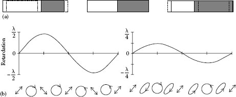
FIGURE 25.1 (a) Optical element and piezoelectric transducer with greatly exaggerated motions in modulation and (b) polarization modulation at peak retardation of half-wave and quarter-wave, respectively.
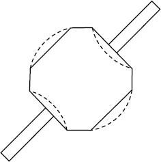
FIGURE 25.2 An “octagonal” PEM with greatly exaggerated motions of the optical element in modulation.
25.2.1 EARLY PEM-BASED STOKES POLARIMETERS IN ASTRONOMY
Kemp, one of the inventors of the PEM, was an astronomical physicist. He employed the PEM in astronomical polarimeters immediately after its invention in order to improve the measurement sensitivity of polarization [33,34,35,36], which he certainly did. Using a PEM solar polarimeter, Kemp and coworkers made it possible to measure accurately the small magnetic circular polarization of light rays emanating from different astronomical objects in the early 1970s [33,34]. In subsequent work, they developed a modified PEM solar polarimeter that achieved an absolute polarization sensitivity of parts per 10 million [35], which may still be the record today for the highest sensitivity obtained by a polarimeter.
In their solar polarimeter, Kemp and coworkers used the simplest PEM arrangement to achieve their extremely high sensitivity in polarization measurements. The Stokes parameters, I, Q, U, and V, were measured using a single PEM followed by a polaroid analyzer as shown in Figure 25.3. Using this setup, Q and U cannot be measured simultaneously. One of the two sets of Stokes parameters, (I, Q, and V) or (I, U, and V), is measured first, then the other is measured after rotating the PEM–analyzer assembly by 45°.
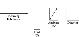
FIGURE 25.3 A single PEM setup for Stokes polarimeter.
Kemp’s success in achieving high sensitivity was the result of both using the PEM and meticulously carrying out the experiments. For example, Kemp and coworkers analyzed and eliminated the surface-dichroism effect of the PEM, etched edge faces of the PEM to remove strain, used average of measurements at several cardinal positions, and carefully considered the alignment of the PEM and the analyzer [33,35]. They claimed that no optical components of any kind should intervene between the observed source and the principal polarimeter element, not even the telescope. Researchers today still find value in their advice for obtaining high-sensitivity polarization measurements.
25.2.2 IMAGING STOKES POLARIMETERS USING THE PEM
Since Kemp’s applications of the PEM in point-measurement astronomical Stokes polarimeters [33,34,35,36], researchers have investigated applying the PEM to imaging polarimeters. The main challenge to using the PEM with the charge-coupled device (CCD) is that the readout of the CCD is too slow for the PEM modulation (tens of kHz). Several methods have been proposed and tested for PEM–CCD applications [37,38,39,40,41,42]. I will briefly describe two examples for solving this problem.
The group at the Institute for Astronomy, ETH Zurich, Switzerland, has long been involved in developing imaging Stokes polarimeters using PEMs and other modulators [37,38,39,40]. The ZIMPOL (Zurich imaging polarimeter) I and II are two generations of state-of-the-art imaging polarimeters. This group, led by Prof. Stenflo, has used the ZIMPOL with different telescopes. Combined with large aperture telescopes, the ZIMPOL provides reliable polarization images with a sensitivity of better than 10−5 in DOP, and thus obtains a rich body of polarization information for non–solar systems, the solar system, and second solar spectrum [43,44].
The ETH Zurich group overcame the incompatibility between the fast PEM modulation and slow CCD readout in an innovative way. Their approach was to use a commercially available CCD that allows the charges to be shifted laterally at a very fast rate. They created a mask to expose only desired rows of pixels on the CCD in synchrony with the modulation frequency (or harmonics) of the PEM. The unexposed pixels thus acted as hidden buffer storage areas within the CCD sensor. The CCD readout was done after thousands of cycles of photocharge between different rows of pixels on the CCD. In ZIMPOL I, they had every second pixel row masked to record two Stokes parameters simultaneously. In ZIMPOL II, they had three rows masked and one row open in each group of four pixel rows, which allowed all four Stokes parameters to be recorded simultaneously.
It is worth noting that ZIMPOL can be used with different types of modulators, such as PEMs, Pockels cells, and ferroelectric liquid crystal modulators. To measure all four Stokes parameters simultaneously, two modulators are required to work in synchronization [37]. The resonant feature of the PEM, a key in providing superior optical properties, makes it difficult to synchronize two PEMs in phase and with long-term stability. In fact, the long-term stability of two synchronized PEMs has not been achieved successfully despite significant effort spent in electronic design [45]. However, practically all published scientific results from ZIMPOL are based on the use of PEMs. Prof. Stenflo in a recent review paper [44] explained why his group chose the PEM over other modulators for their scientific observations. He attributed the success of the PEM to its superior optical properties in polarimetric applications as compared to other types of modulators.
In ZIMPOL II, the synchronized PEM approach was dropped and a single PEM was used. The polarization modulation module in ZIMPOL II is similar to the configuration shown in Figure 25.3. The images of I, Q, and V are recorded first; then the images of I, U, and V are recorded after rotating the polarization modulation module by 45°. The ETH Zurich group has reported a large collection of images of Stokes parameters that were recorded by the ZIMPOL using different telescopes for the sun and other astronomical objects.
Another method of using PEMs in imaging polarimeters has been developed by Diner (Jet Propulsion Laboratory, JPL) and coworkers. The goal of this group was to develop a multiangle spectropolarimetric imager (MSPI) for aerosol satellite remote sensing. High sensitivity in measuring degree of linear polarization (DOLP) is again one of the major challenges. After evaluating different types of polarization modulators, including rotating wave plate and ferroelectric liquid crystal modulators, this group selected the PEM for its application [41,42].
The approach selected by Diner and coworkers involves using two PEMs with a small difference in frequencies. When such a PEM pair is placed in the optical path, the detector signal contains both a high-frequency (PEM modulated) component and a low-frequency component (~10 Hz, this being the beat frequency of the two PEMs) in the waveform. The line readout integration time (1.25 ms) is long enough to average out the high-frequency signal (tens of kHz) and is fast enough to acquire plenty of samples in a beat frequency cycle [41,42]. The signal at the beat frequency is related to Stokes parameters Q and U. The Stokes parameter V is not measured in this application due to its insignificance (<0.1%) in aerosol remote sensing.
The polarization modulation module contains two quarter-wave plates, two PEMs at slightly different modulating frequencies, and an analyzer that can be set at either 0° or 45° [41,42]. In this optical configuration, the Stokes parameters Q and U have the following relationship to I0 and I45, which are the intensities measured when the analyzer is set at 0° and 45°, respectively:
where ωb is the beat frequency of the two PEMs. Therefore, normalized Stokes parameters Q/I and U/I can be measured at the beat frequency. The first results of an imaging Stokes polarimeter using this approach are promising [42]. The program integrating this imaging polarimeter into the satellite remote sensor is still ongoing.
25.2.3 LABORATORY DUAL PEM STOKES POLARIMETERS
For a laboratory point-measurement Stokes polarimeter, while different instrumental configurations have been used [46], the most common dual PEM configuration is shown in Figure 25.4. The key polarization modulation components of the Stokes polarimeter are two PEMs oriented at 45° apart and an analyzer that bisects the axes of the two PEMs [47]. Using this dual PEM configuration, Stokes parameters Q, U, and V can each be measured at a specific harmonic of a PEM. Namely, Q and U can be measured at the second harmonics (2F) of the two PEMs and V can be measured at the first harmonic (1F) of the first PEM. An advantage of this approach is that no cross-terms are used in measuring the Stokes parameters.
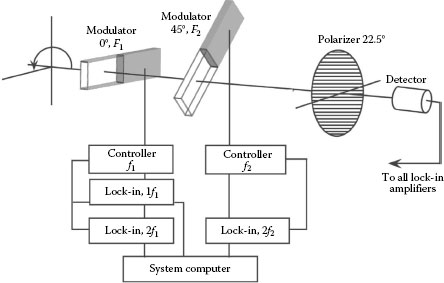
FIGURE 25.4 A typical dual PEM Stokes polarimeter.
The optical train of the dual PEM Stokes polarimeter shown in Figure 25.4 can be analyzed using Mueller matrix calculus. The time varying signal generated on the detector is
where
ω1 and ω2 are the modulation frequencies of the two PEMs
δ10 and δ20 are the peak retardation amplitudes of the two PEMs
δ1 and δ2 are the time-varying phase retardations of the two PEMs (δ1 = δ10 sin ω1t; δ2 = δ20 sin ω2t)
When sin δ1, cos δ1, sin δ2, and cos δ2 in Equation 25.6 are expanded with the Bessel functions of the first kind, we have
where the subscripts of the Bessel functions indicate their orders. As seen in Equation 25.7, Q, U, and V can be determined by detecting the 2F signals of both PEMs (the cos(2ω1t) and cos(2ω2t) terms) and the 1F signal of the first PEM (the sin(ω1t) term).
The DC signal can be derived from Equation 25.7 to be
where all AC terms that vary as functions of the PEMs’ modulation frequencies are omitted, because they have no net contribution to the averaged DC signal. In practice, a low-pass electronic filter can be used to eliminate such oscillations. As seen from Equation 25.8, it is convenient to choose the peak retardation amplitudes of both PEMs to be δ10 = δ20 = 2.405 rad (0.3828 waves) so that J0(δ10) = J0(δ20) = 0. Then the DC signal will be independent of light polarization (Q, U, or V) and thus will directly represent the light intensity from the light source.
When the polarization state of a light beam is the primary concern, normalized Stokes parameters are commonly used. In the dual PEM Stokes polarimeter, the ratios of PEM modulated signals to the average DC signal are used to calculate normalized Stokes parameters, as shown in Equation 25.9:
where V2,2F, V1,2F, and V1,1F represent the strengths of the 2F signals of both PEMs and the 1F signal of the first PEM, respectively.
The electronic signals generated at the detector have both AC and DC components. When lock-in amplifiers are used to demodulate the signals, three lock-in amplifiers are needed to detect Q, U, and V simultaneously. When it is not necessary to measure Q, U, and V simultaneously, one or two lock-in amplifiers can be used for sequential measurements. Alternatively, one can use a fast digitizer to capture the waveform generated at the detector. The waveform is the combined result of all the modulation frequencies generated by both PEMs. Fourier analysis of the digitized waveform (hereafter the digital signal process, or DSP method) gives the signals at the first and second harmonics of both PEMs, thus the Stokes parameters.
25.2.4 DUAL PEM STOKES POLARIMETER USED IN THE TOKAMAK
The dual PEM Stokes polarimeter has been successfully applied to Tokamak plasma (ionized gas) diagnostics. A Tokamak is a machine for confining the plasma using a magnetic field. The Tokamak was originally conceived in 1950 by then Soviet scientists I. Tamm and A. Sakharov. The term “Tokamak” is the translation of a Russian word which itself is an acronym of Russian words [48]. There are several Tokamaks in the world including the DIII-D in the United States, JET in the United Kingdom, and the upcoming ITER in France [49]. The Tokamak is the most researched nuclear fusion reactor and is considered to be a promising fusion power generator.
In a Tokamak, a relatively constant electric current in the toroidal coils creates a relatively constant toroidal magnetic field. The moving ions and electrons in the plasma (toroidal plasma current) create a poloidal magnetic field. The total magnetic field at any location inside the plasma is the combination of the toroidal and poloidal fields as shown in Figure 25.5. The so-called magnetic field pitch angle is defined as
The toroidal magnetic field is known from the electric current supplied to the toroidal coils. If the magnetic field pitch angle is measured, the poloidal magnetic field and thus the plasma current can be calculated. The plasma current profile can be determined from the magnetic field pitch angles measured at different locations in the plasma. To achieve high stability and confinement in a Tokamak, it is critical to monitor and control the distribution of plasma current.
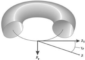
FIGURE 25.5 A diagram showing the relationship between the toroidal and poloidal magnetic fields in a Tokamak.
The motional Stark effect (MSE) polarimeter was first developed by Levinton and coworkers to determine the magnetic field pitch angle in the plasma of a Tokamak [50,51]. The MSE polarimeter was extended by Wroblewski and Lao to a multichannel polarimeter to determine the plasma current profile in the DIII-D Tokamak [52]. This method has now been applied to most of the Tokamaks in the world as a standard diagnostic instrument.
In a Tokamak, if a high-energy neutral deuterium beam is injected into the plasma, as the injected deuterium beam propagates inside the plasma, the deuterium atoms are subjected to an electric field that is generated by their motion across the magnetic field. Namely, E = Vbeam × B where Vbeam is the velocity of injected beam, B is the local magnetic field, and E is the local electric field generated by the motion across the magnetic field. The Stark effect [53] refers to spectral splittings due to an external electric field. The electric field generated by the motion of deuterium atoms across a magnetic field produces splittings in the spectrum of the Balmer-α emission of the injected deuterium beam. This effect is called the MSE.
The MSE polarimeter takes advantage of polarized emission due to the Stark effect to measure the magnetic field pitch angle. In addition to the spectral splittings, the MSE produces polarized emissions according to the selection rules for atomic electronic transitions. Emission spectral lines from the Δm = ±1 transitions, or the σ components, are particularly useful to the MSE polarimeter. The σ component emissions are linearly polarized, and the polarization direction is perpendicular to the electric field and parallel to the local magnetic field. By measuring the two linear polarization parameters, Q and U, of the Balmer-α emissions from the injected deuterium atoms, the MSE polarimeter determines the magnetic field pitch angle at the intersection of the injected beam and the observation direction. In a multichannel MSE polarimeter, the magnetic field pitch angles at multiple locations inside the plasma are measured simultaneously. Figure 25.6 shows a block diagram of using an MSE polarimeter in the Tokamak.
The PEMs used in the MSE polarimeter have some special features unique to this application. They have symmetrical optical elements (square with the four corner cut off for mounting). A symmetrical optical element in the PEM provides symmetrical modulation distribution over its aperture. The PEMs for this application have large optical apertures. Since the PEM is a resonant modulator, its size is inversely proportional to its resonant frequency. Modern MSE polarimeters use 20 and 23 kHz PEMs specially designed into a single enclosure as shown in Figure 25.7. Since MSE polarimeters use optical fibers to link to multiple measurement locations in the plasma, the symmetrical retardation distribution and large optical aperture of the 20/23 kHz PEM pair allow simultaneous, multichannel measurements using the same MSE polarimeter. Finally, the PEM electronics are magnetically shielded and separated 10–15 m from the strong magnetic field in the plasma.
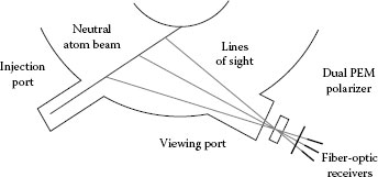
FIGURE 25.6 A diagram showing an MSE polarimeter used in a Tokamak.
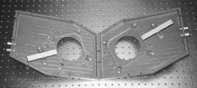
FIGURE 25.7 A photo picture of the 20/23 kHz PEM pair used in a modern MSE polarimeter.
25.2.5 COMMERCIAL DUAL PEM STOKES POLARIMETERS
25.2.5.1 Visible Stokes Polarimeters
Several models of dual PEM Stokes polarimeters have become commercially available from Hinds Instruments, including laser polarization analyzers and spectroscopic Stokes polarimeters in the UV–vis, near IR, and mid-IR spectral regions [18]. In one model, a DSP method is used to calculate Stokes parameters using Fourier analysis. Using this DSP method, the dual PEM Stokes polarimeter measures all normalized Stokes parameters simultaneously at a rate of >350 sets of data per second [54].
To test this polarimeter, a mechanical “chopper wheel” was modified to simulate a light source with controlled, yet fast changing polarization states. This “chopper wheel” consists of a polymer film retarder in one half and an open space in the other half. The retarder film has an average linear retardation of ~280 nm with significant variations over its aperture. The spin rate of the wheel is regulated by the controller of a mechanical chopper. In an experiment, the polarization of a linearly polarized He–Ne laser (632.8 nm) was set at approximately −45°. The light polarization was further purified with a calcite prism polarizer that was precisely oriented at −45.0°. The modified “chopper wheel” was placed between the laser–polarizer combination and the dual PEM Stokes polarimeter and was spun at 2 turns per second during the experiment. A typical set of data obtained in this experiment is depicted in Figure 25.8a through c.
Figure 25.8a shows five repeated patterns of the normalized Stokes parameters (five cycles) measured in 2.5 s. The rate of data collection for this experiment was 371 sets of normalized Stokes parameters per second. As the “chopper wheel” rotated one full turn (one cycle of repeated pattern in Figure 25.8a), the laser beam passed through the opening (i.e., no retardation) for half of the time. During this half-cycle, the polarization of the laser was unchanged. As shown in Figure 25.8a, we observed for this half-cycle that UN = −1, QN = 0, VN = 0, which represents linearly polarized light at −45°. For the other half-cycle, QN, UN, and VN all changed significantly as the laser beam passed through different locations of the rotating retarder.
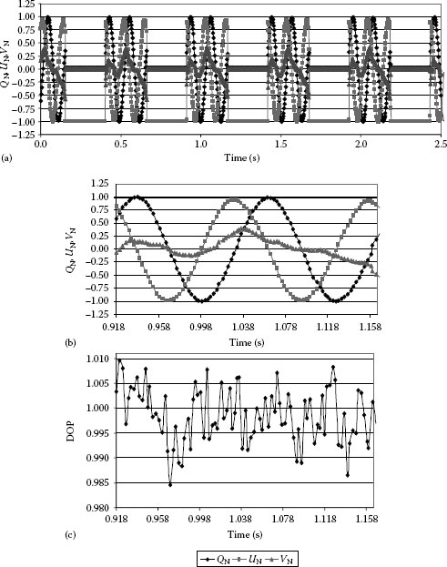
FIGURE 25.8 (a) Normalized Stokes parameters measured as the “chopper wheel” was spun at 2 turns per second; (b) Figure 25.8a expanded to show a half-cycle when the laser beam passes the retarder; (c) DOP during the half-cycle illustrated in Figure 25.8b.
Figure 25.8b, which is an expansion of Figure 25.8a, illustrates in detail how each normalized Stokes parameter varied during the half-cycle when the laser beam passed through the retarder. The polarization state of the light beam after passing the polymer film was dominated by the linear components, QN and UN. This is because the polymer film used in the “chopper wheel” was fairly close to a half-wave retarder. If an exact half-wave retarder was used, it would rotate just the plane of the linearly polarized light beam. There would have been no circular polarization component. The weak circular component (VN) seen in Figure 25.8b is due to the deviation from half-wave retardation of the polymer retarder.
During the other half-cycle, when the light beam goes through the opening, we typically observed an UN of −1.00 with a standard deviation of ~0.0004. For example, the data in the next half-cycle following the data shown in Figure 25.8b have an average UN of −0.9922 and a standard deviation of 0.00036.
Figure 25.8c displays the DOP during the half-cycle illustrated in Figure 25.8b. Although QN, UN, and VN all varied significantly, the DOP changed little during this half-cycle, since the depolarization of the retarder is negligible. The data plotted in Figure 25.8c have an averaged DOP of 0.994 and a standard deviation of 0.0054.
Notice the significant difference in the standard deviations of DOP for the two halves (0.0054 vs. 0.00036) in a full cycle as the “chopper wheel” spun a full turn. The lower standard deviation, which was measured during the half-cycle when the light beam passed the opening, represents the repeatability of the instrument. The higher standard deviation of DOP is primarily due to “mechanical noise.” The polymer film retarder used in the “chopper wheel” had some floppiness. The floppiness, coupled with the mechanical spin of the chopper, introduced higher noise to the data. This was confirmed by observing increased standard deviation of DOP, 0.0089 and 0.0097, when the spin rate of the “chopper wheel” was increased to 4 and 7 turns per second, respectively.
Finally, the 370 sets of data per second is a fast speed for collecting data, particularly with the high repeatability and accuracy obtained at this rate. However, this rate is still far below the limit imposed by the PEMs.
As an alternative to the DSP method, lock-in amplifiers can be used for signal processing in the same dual PEM Stokes polarimeter. When lock-in amplifiers are used for signal processing, each one can be used to detect a signal at a specific modulation frequency. The full dynamic range of the lock-in amplifier can thus be used in demodulating that particular signal. High-quality lock-in amplifiers are still the best demodulators currently available for many PEM-based instruments, particularly when the measurement speed is not critical. The extremely high sensitivity in measuring low DOP that was achieved by Kemp attests to the powerful measurement capability of the PEM, lock-in amplifier, and careful experimentation.
One application of the polarimeter described in this section is to monitor the polarization quality of a laser. Figure 25.9a through e shows the measured result of a randomly polarized laser (sometimes mistakenly called an unpolarized laser). As seen in Figure 25.9a, the DC signals exhibit sharp and frequent intensity variations even though the total percentage of the variations is small.
Figure 25.9b through d illustrates fairly significant variations in all three normalized Stokes parameters. In particular, QN and UN have a much higher magnitude than VN, which indicates a much higher degree of varying linear polarization in the laser. Figure 25.9b and c shows that QN and UN reach “0” at the same time where the laser beam is nearly unpolarized. QN and UN also reach maxima or minima at the same time, though with opposite signs. At these data points the laser beam has a fairly high DOLP. The variation in the DOP of this randomly polarized laser, shown in Figure 25.9e, reveals that this laser does not output randomly polarized light even when the integration time is on the order of 1 s, and it does not produce a light beam with a constant DOP. For this reason, a randomly polarized laser is avoided in building polarization sensitive instruments.
25.2.5.2 Near-Infrared Fiber Stokes Polarimeters
Based on the same principle, a near-infrared (NIR) Stokes polarimeter is made commercially available for applications using optical fibers [91]. In the light source module shown in Figure 25.10a, there is a 1550 nm diode laser followed by a linear polarizer. A single mode fiber connects the light source module to the Stokes polarimeter. The polarimeter is used to measure the normalized Stokes parameters for the light beam entering it from the fiber. Three manual fiber stretchers are attached to the fiber to generate different polarization states for testing the polarimeter. During a test of this polarimeter, the three fiber stretchers were manually operated in a random fashion to generate arbitrary polarization states for the light beam entering the polarimeter. A typical set of data is shown in Figure 25.10b. In the middle part of the dataset, all three normalized Stokes parameters changed as the fiber was stretched by the stretchers. Although the polarization states of the light beam changed, the DOP remained constant at 1.00, which indicates negligible depolarization in the stretched fiber. At both ends of the dataset shown in Figure 25.10b, all normalized Stokes parameters remained constant when the fiber stretchers were not moved.
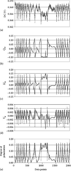
FIGURE 25.9 Measured Stokes parameters for a randomly polarized He–Ne laser (632.8 nm). (a) DC; (b) QN; (c) UN; (d) VN; and (e) degree of polarization.
In addition to testing optical fibers, this Stokes polarimeter can be used in other applications. In fact, this polarimeter was originally built for monitoring the level of a weak magnetic field. In that application, a special fiber, made from a material with a high Verdet constant, was placed in a weak magnetic field. The strength of the magnetic field was determined from the Faraday rotation measured by the polarimeter.
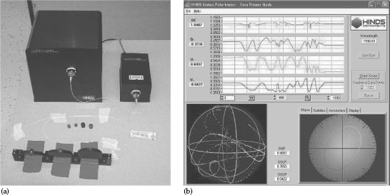
FIGURE 25.10 (a) A photo picture of an NIR Stokes polarimeter for fiber applications and (b) a typical set of data obtained on the NIR Stokes polarimeter.
25.2.5.3 Spectroscopic Stokes Polarimeter
Spectroscopic polarimetry, combining the rich information from both spectroscopy and polarimetry, is one of the most exhaustive methods for analyzing light properties and light–matter interaction. It is applied to a wide range of scientific disciplines. In searching for life in the universe, we need a sensitive remote sensor capable of identifying a universal biosignature. Since all known living materials contain chiral molecules (a molecule that does not superimpose with its mirror image) possessing almost exclusively a single handedness in their biological processes, homochirality is likely to be a universal biosignature for all biochemical life whether similar to terrestrial or not. A PEM-based spectroscopic Stokes polarimeter is well suited to both remote sensing and detecting weak circular polarization signals that may arise from homochirality of astrobiological samples.
The PEM-based spectroscopic Stokes polarimeter [92] is designed to work at low light levels that are typical in astronomical applications. It is optimized to detect a circular polarization signal that is orders of magnitude weaker than a linear polarization signal. This polarimeter can work in different laboratory configurations. In the application described in this section, the polarimeter is mounted to an integrating sphere to allow operation in either transmissive or reflective mode. The integrating sphere randomly diffuses the illumination so that it is averaged over incident directions to minimize possible artifacts from linearly polarized light. A block diagram of this polarimeter and the integrating sphere is shown in Figure 25.11. For future applications, this polarimeter is designed to be mounted to telescopes.
Using this polarimeter, we studied whether photosynthetic microbes produce a macroscopic circular polarization signature in scattered light [93,94]. If photosynthetic microbes do produce such a signature, it could be used in remote sensing as a powerful indicator of the presence of a universal biosignature, namely, homochirality. In a series of experiments, we used this polarimeter to detect the small circular polarization present in light scattered by photosynthetic microorganisms and macroscopic vegetation. We obtained cultures of photosynthetic marine cyanobacteria that possess chlorophyll a and antenna pigments phycocyanin and phycoerythrin. For context, we measured examples of macroscopic vegetation chosen largely by availability near the laboratory, and control minerals iron oxide, sulfur (which has a strong spectral “edge”), and a Mars regolith analog. The detailed results may be found in Refs. [93,94].
A comparison of the transmission and absorption polarization spectra for specimen Synechococcus WH8101 is presented in Figure 25.12 [93].
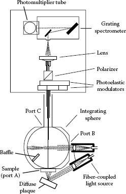
FIGURE 25.11 Block diagram of the spectroscopic Stokes polarimeter and the integrating sphere to allow operation in either transmissive or reflective mode.
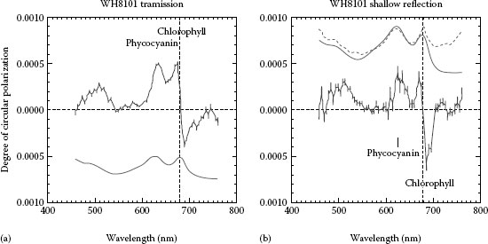
FIGURE 25.12 Circular polarization spectra of cyanobacteria WH8101. (a) Transmission polarization spectrum of Synechococcus WH8101. The line above shows the degree of circular polarization, with ±1σ uncertainty; the solid line below shows a scaled version of the absorbance spectrum. (b) Reflection polarization spectrum as for Figure 25.12a except that the solid line is scaled −log10(Reflectance) and the dashed line is a scaled plot of linear polarization degree.
The strongest circular polarization features in both transmission and absorption are related to the electronic absorption bands of the photosynthetic pigments. This result characterizes all the results we obtained on cyanobacteria, as presented in Refs. [93,94]. The circular polarization peaks across the well-defined photosynthesis absorption bands, and in the case of chlorophyll a, there is a very distinctive sign change at the location of the absorption maximum. This has important consequences for the likelihood of a large-scale macroscopic polarization being present. Oceanic concentrations of microbes are low compared to our laboratory specimens, but with modest volume, the optical depth can be unity and dominated by chlorophyll and cyanobacteria. Hence, there is the possibility that the oceans will yield a measurable circular polarization signal.
We also acquired polarization spectra of a variety of leaves. Leaf circular polarization reflection spectra show substantial diversity, but the average brings out common features. Figure 25.13a and b exhibits a strong polarization signal associated with chlorophyll absorption between 650 and 700 nm and a broader spectral dependence of polarization to the blue. Polarization is low at wavelengths longer than the chlorophyll red edge at 700 nm. In a planetary context, it will be of interest to establish the polarization characteristics of large-scale, sometimes heterogeneous, vegetation-dominated scenery with empirical measurements.
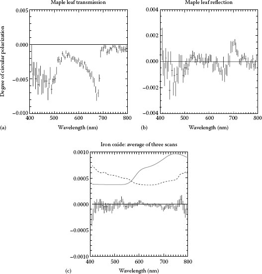
FIGURE 25.13 Circular polarization spectra for a leaf and a mineral. (a) A maple leaf transmission polarization spectrum. (b) Corresponding maple leaf reflection polarization spectrum. (c) A control iron oxide polarization spectrum. The data points with error bars are the degree of circular polarization in each panel. The solid line of Figure 25.13c shows the reflection spectrum of iron oxide and the dashed line, the degree of linear polarization, both arbitrarily scaled.
As controls we made measurements of two minerals exhibiting significant strength “edges” in their spectra: iron oxide and sulfur [93,94]. This also served to guard against potential instrumental artifacts in the vicinity of rapidly changing light levels. Figure 25.13c shows the polarization spectrum of the iron oxide. The mineral spectra show no relationship between polarization and intensity, unlike the vegetation, and polarization is low overall. Additional polarization spectra of a variety of other minerals were presented in Ref. [93], and this was true in all cases.
Using this instrument, we have quantified the circular polarization signal produced by astrobiologically relevant microorganisms and compared the results to macroscopic vegetation (such as leaves) and abiotic minerals. We see unambiguous circular polarization from photosynthetic microbes. Therefore, circular polarization spectroscopy offers the prospect of remotely sensing life’s unique chiral signature. Beyond the laboratory, we hope to test such a polarimeter in an airborne instrument looking at the Earth.
25.3 MUELLER MATRIX POLARIMETER
25.3.1 DUAL PEM MUELLER MATRIX POLARIMETER
The Mueller matrix polarimeter can be used to determine all 16 elements of the Mueller matrix, thus the complete polarization-altering properties of a sample. The most studied Mueller matrix polarimeter is perhaps based on the dual rotating wave plate design, for which there are many published articles [2,55,56,57]. When PEMs are employed to obtain a higher measurement sensitivity [58,59,60,61], the dual PEM configuration, shown in Figure 25.14, is the setup most commonly used in a Mueller matrix polarimeter. The key elements for polarization modulation in the setup are the polarizer–PEM and PEM–analyzer assemblies.
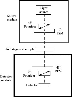
FIGURE 25.14 A block diagram of a dual PEM Mueller polarimeter.
If a normalized Mueller matrix is used for a sample, the signal reaching the detector, Idet, in the setup shown in Figure 25.14, can be derived by using the Mueller matrix calculus:
where
I0 represents the light intensity after the first polarizer
K is a constant representing transmission efficiency of the optical system after the first polarizer
The “DC” signal from Equation 25.11 is
where any AC term that varies as a function of the PEMs’ modulation frequencies is omitted, because they have no net contribution to the averaged DC signal. At J0(2.405) = 0 PEM setting, the “DC” term is simplified to
The useful “AC” terms from Equation 25.11, which are related to eight normalized Mueller matrix elements, are summarized in Equation 25.14.
The eight Mueller matrix elements that can be determined from this optical configuration [P1(45°)-M1(0°)-S-M2(45°)-P2(0°)] and three other optical configurations are provided in Table 25.1.
In Table 25.1, each “x” indicates a Mueller matrix element that cannot be determined using the corresponding optical configurations. A total of four optical configurations is required to determine all Mueller matrix elements. Of course, one may use −45° and 90° instead of 45° and 0° in the aforementioned configurations. The results will be the same after calibrating the signs of the “AC” signals.
TABLE 25.1
Dual PEM optical Configurations and Measured Mueller Matrix Elements
Optical Configurations |
Measured Mueller Matrix Elements |
P1(45°)-M1(0°)-S-M2(45°)-P2(0°) |
|
P1(0°)-M1(45°)-S-M2(0°)-P2(45°) |
|
P1(45°)-M1(0°)-S-M2(0°)-P2(45°) |
|
P1(0°)-M1(45°)-S-M2(45°)-P2(0°) |
Jellison championed this dual PEM design and its applications [58,59,60,61]. He developed a dual PEM system for ellipsometric studies and called it two-modulator generalized ellipsometry (2-MGE). He has applied the 2-MGE to measuring retardation and diattenuation properties of both transmissive and reflective samples [60,61,62,63].
25.3.2 FOUR MODULATOR MUELLER POLARIMETER
If one wishes to measure all 16 Mueller matrix elements simultaneously, 4 modulators are required [64,95]. There are many optical configurations to arrange the four PEMs and two polarizers in a complete Mueller polarimeter. Figure 25.15 depicts one of such arrangements of 4 PEMs in order to measure all 16 Mueller matrix elements.
The optical setup in Figure 25.15 generates many modulation frequencies from different combinations of the harmonics of the four PEMs. All 16 Mueller matrix elements can be determined from one or more of the combined modulation frequencies. Table 25.2 lists one modulation frequency corresponding to each Mueller matrix element. Detailed analysis of the four PEM Mueller polarimeter and measured data in both spectroscopic and spatial domains is available in Ref. [95].
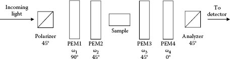
FIGURE 25.15 A block diagram of a four PEM Mueller polarimeter.
TABLE 25.2
Possible modulation Frequencies to Determine Each Mueller matrix Element
Mueller matrix Elements |
PEM Frequencies |
m12 |
ω0 + ω1 |
m13 |
2ω0 |
m14 |
−ω0 − 2ω1 |
m21 |
ω0 |
m22 |
ω2 + ω3 |
m23 |
ω2 + ω3 |
m24 |
ω0 + ω1 − ω2 + ω3 |
m31 |
2ω3 |
m32 |
−ω0 + ω1 − 2ω3 |
m33 |
2ω0 − 2ω3 |
m34 |
ω0 − 2ω1 − 2ω3 |
m41 |
−ω2 + ω3 |
m42 |
ω0 + ω1 − 2ω2 + ω3 |
m43 |
2ω0 + 2ω2 − ω3 |
m44 |
ω0 + 2ω1 − 2ω2 + ω3 |
Note: The four frequencies of the modulators are ω0, ω1, ω2, and ω3.
While it is true that a complete Mueller polarimeter can be used to measure all 16 elements in a Mueller matrix, it is complicated to detect all polarization-altering properties, in terms of retardation, diattenuation, and depolarization, from a measured Mueller matrix [2]. The difficulty is also due to the less well-understood depolarization [65]. Currently, applications of the complete Mueller polarimeter are still rather limited. On the other hand, specific industrial applications often require the determination of just one or two polarization parameters. Hence, special polarimeters have gained a wide range of applications in industrial metrology. In this section, I provide several examples of PEM-based special polarimeters and their applications.
25.4.1 LINEAR BIREFRINGENCE POLARIMETERS AND THEIR APPLICATIONS IN THE OPTICAL LITHOGRAPHY INDUSTRY
25.4.1.1 Linear Birefringence Polarimeter
Figure 25.16 depicts the block diagram of a linear birefringence polarimeter (Exicor®) that the author coinvented [66,67,68]. In this special polarimeter, the optical bench contains a polarization modulation module (a light source, a polarizer, and a PEM), a sample holder mounted on a computer-controlled X–Y stage, and a dual channel detecting assembly.
Each detecting channel contains an analyzer and a detector. Channel 1 (crossed-polarizer) measures the linear retardation component that is parallel to the PEM’s optical axis (0°), and channel 2 measures the linear retardation component that is oriented 45° from the PEM’s optical axis.
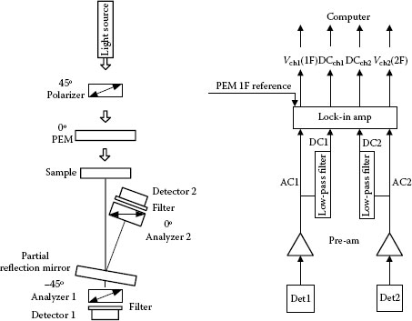
FIGURE 25.16 A block diagram of a linear birefringence polarimeter (Exicor).
Using the Mueller matrix calculus, the light intensities reaching the detectors of both channels are derived to be
Substituting the Bessel expansions into Equation 25.15 and taking only up to the second order of the Bessel functions, we have
The “DC” signals from both detectors are
The ratios of 1F “AC” signals to the corresponding DC signals from both detectors are
where VCh1(1F) and VCh2(1F) are the 1F components of the detector electronic signals from both detectors.
Defining Rch1 and Rch2 as corrected ratios for both channels, Equation 25.18 becomes
When the PEM retardation amplitude is selected to be Δ0 = 2.405 rad (0.3828 waves) so that J0(Δ0) = 0, the magnitude and angular orientation of the linear retardation of the sample are expressed as
where δ, represented in radians, is a scalar. When measured at a specific wavelength (i.e., 632.8 nm), it can be converted to retardation in “nm.”
The accuracy of this instrument was tested using a Soleil-Babinet compensator [70]. Figure 25.17 shows the agreement between the measured data and the values of a calibrated Soleil-Babinet compensator. The experimental data shown in Figure 25.17 lead to a near-perfect linear fit. In the ideal case, the instrumental readings and the corresponding compensator values will be identical (Y = X).
This instrument provides a high repeatability of measurements and a low noise level. Figure 25.18a displays the data of 3000 repeated measurements at a fixed spot of a compound quartz wave plate [69]. These 3000 data points have an average retardation of 11.34 nm with a standard deviation of 0.0078. When the instrument is properly calibrated, the linear retardation readings of the instrument without any sample should be a representation of the overall instrumental noise level. Figure 25.18b displays a collection of ~18,000 data points that was recorded in about 8 h (automatic offset correction was used at 20 min intervals) [69]. This dataset has an average of 0.0016 nm and standard deviation of 0.0009.
When the ratios of the AC and DC signals are used, linear retardation measurements will not be affected by light intensity changes caused by light source fluctuation, sample absorption, partial reflection, and others. In a test, we purposely varied the light intensity to demonstrate this feature of the instrument. The raw data of AC and DC signals for both detecting channels at different light intensities, along with the retardation values determined from AC/DC, are presented in Figure 25.19a and b. As seen, the retardation magnitude and fast axis angle of the sample remain constant as the light intensity is reduced [69]. As expected, the measurement errors for retardation increase when the light intensity becomes very small.
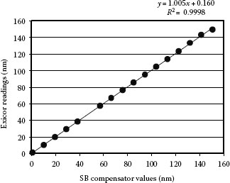
FIGURE 25.17 Measured values on Exicor vs. calibrated values of a Soleil-Babinet compensator.
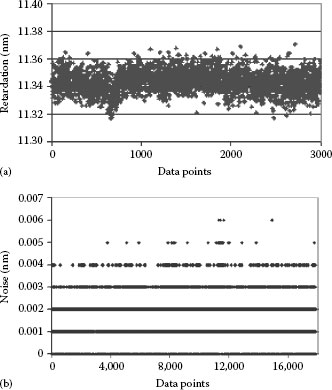
FIGURE 25.18 (a) A typical dataset for instrumental stability and (b) a typical dataset for instrumental noise.
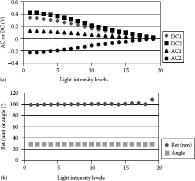
FIGURE 25.19 (a) Raw data of AC and DC signals from both detecting channels and (b) retardation magnitude and angle calculated from AC/DC with decreasing light intensities.
25.4.1.2 Linear Birefringence in Photomasks
In the semiconductor industry, fused silica is the standard material for the lenses and photomask substrates used in modern optical lithography step and scan systems. To follow Moore’s law (doubling the number of transistors per integrated circuit every 18 months) [71], the semiconductor industry continuously moves toward finer resolution by adopting shorter wavelengths and other resolution enhancement means. Linear birefringence in optical components can degrade the imaging quality of a lithographic step and scan system through several effects including bifurcation, phase front distortion, and alternating light polarization. Consequently, the requirement for low-level residual birefringence in high-quality optical components, including photomasks, has become stringent.
The linear birefringence polarimeter described earlier, with its high accuracy and sensitivity (<0.005 nm), is particularly suited to the quality control of photomask substrates, or photomask blanks. Photomask blanks are made of high-quality fused silica that has low levels of linear retardation, low color centers, and well-polished surfaces. They have negligible circular birefringence, depolarization, and diattenuation (at normal incidence). Low-level linear birefringence due to residual stress in photomask blanks is the primary concern of this industry.
Figure 25.20 shows the birefringence images of four fused silica photomask blanks (6” × 6”; thickness: 0.25”) [72,73]. In Figure 25.20a through d, the magnitude of retardation is color-coded. Three of the four samples (Figure 25.20a, b, and d) display a retardation level generally below 3 nm. The angle of fast axis at each data cell is described with a short bar. Figure 25.20a through d shows different patterns of residual linear retardation in these photomask blanks. The different patterns and levels of residual linear retardation in the mask blanks reveal the residual strain formed during annealing and other manufacturing processes.
For over 20 photomask blanks measured, the birefringence pattern of Figure 25.20a was observed most often. Photomask blanks exhibiting such a birefringence pattern have a wide range of residual retardation levels. Three other examples are shown in Figure 25.21a through c with maximum retardation levels at ~20, ~10, and ~4 nm, respectively, as measured at 632.8 nm [72,73]. All three photomask blanks have a similar birefringence angle pattern as shown in Figure 25.21d.
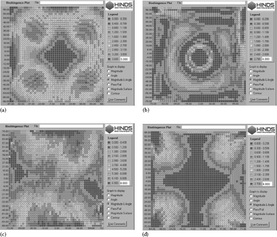
FIGURE 25.20 Overlaid images of retardation magnitude and fast axis angle for photomask blanks (a–d; fused silica; 6” × 6” × 0.25”; spatial resolution: 3 mm).
The images of linear birefringence shown in Figure 25.21a through d have some common features. In each photomask blank, four areas along the edges of the blank exhibit the highest levels of retardation. Fortunately, these areas are at the periphery of a photomask blank. It is unlikely that die patterns will overlap these regions when a photomask is made. Therefore, the residual birefringence in those areas, although high, may not affect the image projected onto the wafer. There are four inner regions, shown in Figure 25.21a through c, with high levels of residual linear retardation. These four peak areas, as shown in the birefringence surface plots, are fairly close to the center of the photomask. They would overlap with the die patterns on a photomask, especially if a photomask contains more than one die. Furthermore, Figure 25.21d shows that the fast axis angles at those four inner high retardation areas are close to ±45°.
Figure 25.22a and b illustrates two typical linear birefringence images of photomasks with low density of features [73]. For both samples, the die patterns are located in the central part of the photomasks. The retardation map shown in Figure 25.22a exhibits a maximum retardation that is below 5 nm and an angular pattern of fast axis that closely resembles that shown in Figure 25.21d. In Figure 25.22a, there are two gray bars that carry no birefringence information. The two gray bars represent the approximate location of two “chrome” rails on this photomask that blocked the light beam completely during measurement. The smooth flow of the birefringence angle pattern inside and outside of the die area demonstrates that the “chrome” features on the photomask have no significant effect on linear birefringence, at least at the retardation level shown in Figure 25.22a.
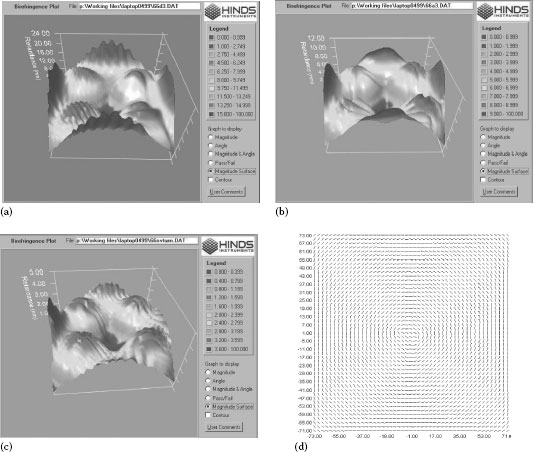
FIGURE 25.21 (a–c) Linear retardation images for photomask blanks—surface plots and (d) angle plot (fused silica; 6” × 6” × 0.25”; spatial resolution: 3 mm).
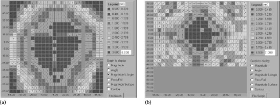
FIGURE 25.22 (a and b) Linear retardation images of two fused silica photomasks (fused silica; 6” × 6” × 0.25”; spatial resolution: 5 mm).
Figure 25.22b is the linear retardation image of a photomask with four die patterns located in the central area of this photomask. Figure 25.22b shows a maximum retardation below 7 nm and a birefringence angular pattern that closely resembles the patterns depicted in Figure 25.21d. It further confirms that the “chrome” features on a photomask have little effect on the residual birefringence at the retardation level shown here.
The experimental results for the two photomasks measured here indicate that the residual linear birefringence in a photomask is primarily due to the contribution from the substrate, rather than from the “chrome” features formed on the substrate. When the residual linear birefringence in a photomask blank is reduced to a much lower level, one would expect that the “chrome” features should have some effect on the mechanical stress pattern of the photomask substrate.
25.4.1.3 Effect on Image Quality Due to Linear Birefringence in a Photomask
In general, a high level of residual birefringence in an optical component can lead to aberrations in polarization ray tracing. Low linear birefringence in a photomask is particularly important for producing high-quality wafers. In an optical lithographic step and scan system, there may be over 20 optical components adding to a total thickness of optical materials exceeding 1 m. The residual linear birefringence integrated over the entire path-length of the optical components should be much larger than the birefringence in a photomask. However, a photomask is the only component in the optical path that will be changed from time to time in a given step and scan system. Assuming that a calibration can effectively eliminate the effect of residual linear birefringence in all fixed optical components in a step and scan system, the residual birefringence in a photomask would become a significant factor affecting the imaging quality formed on the wafer.
There are a variety of different designs in optical lithographic step and scan systems. For example, a design using all refractive lenses is called the refractive design; a design using mixed reflective and refractive optical components is called the catadioptric design [74]. The same residual linear birefringence in a photomask could have a different impact for step and scan systems with different designs. Of the various types of step-scan systems, linear birefringence in a photomask makes the largest impact on imaging quality in a particular catadioptric system [75].
The key component of this catadioptric design [75] is a polarization beam splitter. Its basic function is illustrated in Figure 25.23. Imagine that a linearly polarized light beam enters the beam splitter with the polarization direction of the beam normal to the plane defining the page you are reading. The light beam is reflected up at the interface of the polarization beam splitter; then the light beam exits the beam splitter with no change in polarization. Passing the quarter-wave plate, the light beam becomes right circularly polarized. Reflected by the mirror, the light beam changes to left circularly polarized. Passing the quarter-wave plate again, the light beam becomes linearly polarized along the horizontal direction in the plane defining the page you are reading. The horizontally polarized light beam enters the beam splitter again, passes the interface with no further change in its polarization, and finally exits the beam splitter. The die pattern on the photomask is imaged to the photoresist layer on the wafer. Note that the elaborately designed lens groups for an optical lithographic system [75] are omitted in Figure 25.23.
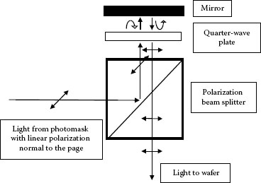
FIGURE 25.23 A block diagram for the polarization beam splitter used in a catadioptric design.
As illustrated in Figure 25.23, the light intensity pattern created by the photomask is perfectly imaged onto the wafer if there is no linear birefringence in the photomask substrate. What happens if the photomask substrate has the linear retardation pattern as shown in Figure 25.21a through c. Let us assume that the four inner peak areas have linear retardation values ~10 nm with the fast axes at either 45° or −45°. The linearly polarized light, passing through the four inner high birefringence areas, will become elliptically polarized. The elliptically polarized light can be decomposed into a linear polarization component and a circular polarization component. The linear component will pass through the beam splitter as illustrated in Figure 25.23. A retardation of 10 nm with its fast axis angle 45° from the incident polarization will result in a circular polarization component of ~10% at 193 nm. Half the intensity of the circular component will be lost when the light beam goes through the polarizing beam splitter. Therefore, a specific light intensity pattern correlated to the linear birefringence pattern in the photomask substrate is imaged onto the wafer, which significantly distorts the image of the photomask.
However, if the linear birefringence in a photomask substrate is controlled to below 2 nm, the maximum circular polarization component produced at 193 nm will be <0.5%. The distortion of the image due to the linear birefringence in the photomask substrate will not exceed 0.25%. Furthermore, the retardation pattern shown in Figure 25.21 generates the maximum image distortion in this catadioptric step and scan system. Such a retardation pattern is likely caused by an imperfect process for annealing the photomask substrate. When the manufacturing process is refined and the maximum value of residual retardation in a photomask is controlled to below 2 nm, the angular pattern of residual birefringence may be significantly different from the pattern shown in Figure 25.21d, which will have an even smaller impact on degrading the imaging quality.
Finally, fused silica photomask blanks containing levels of residual retardation as high as that shown in Figure 25.21 are unusual in the industry today. Once the problem in photomask blanks was identified, the industry moved quickly to correct the problem. Consequently, using the special polarimeter, the material suppliers have the linear birefringence in photomask substrates well controlled.
25.4.1.4 Deep Ultraviolet Linear Birefringence Polarimeter
The 633 nm linear birefringence polarimeter does not measure birefringence at the working wavelengths of the optical lithography industry. So, the industry needed a deep ultraviolet (DUV) linear birefringence polarimeter to provide at-wavelength measurements.
The need for a DUV linear birefringence polarimeter was further accelerated by the development of a 157 nm lithographic tool several years ago. In a 157 nm step and scan system, calcium fluoride would become the primary optical material. CaF2 is a single crystal that belongs to the cubic group with high degrees of symmetry (i.e., fourfold and threefold rotation axes). It is generally thought that single crystals in the cubic group have isotropic optical properties including index of refraction [76]. However, Burnett and coworkers reported [77,78] the measurement of intrinsic birefringence (spatial-dispersion-induced birefringence) in CaF2 at UV wavelengths. They found that the intrinsic birefringence of CaF2, (n[−110] – n[001]), is −11.2 ± 0.4 × 10⁻⁷ at 157.6 nm. This birefringence corresponds to a retardation value of 11.2 ± 0.4 nm/cm (normalized to the thickness of a sample) when the light beam propagates along the [110] crystalline axis. The discovery of intrinsic birefringence in CaF2 piqued the industry’s interest in measuring birefringence at 157 nm and other lithographic wavelengths.
In the DUV linear birefringence polarimeter, a dual PEM design, similar to what is shown in Figure 25.11, is selected [79,80]. The light source is a deuterium lamp for optimizing the DUV wavelengths. The wavelength is selected by a monochromator. The choice of a deuterium lamp is due to both economics (high cost of suitable lasers) and flexibility (a deuterium lamp provides a range of DUV wavelengths). The light beam exiting the monochromator is collimated by a calcium fluoride lens. The two PEMs have modulation frequencies of 50 and 60 kHz, respectively. Both the polarizer and analyzer are MgF2 Rochon polarizers. The sample is mounted on an XY scanning stage (450 mm × 450 mm) that is controlled by a PC. The detector is a CsI photomultiplier tube (PMT). The electronic signals generated at the PMT are processed using either lock-in amplifiers or a waveform analysis method developed by Jellison and coworkers [58,59,60].
The theoretical analysis of this optical configuration using the Mueller matrix calculus yields
when the zero-order Bessel function of either PEM is set to 0.
The useful AC terms for determining linear retardation are:
the (2ω1 + ω2) and (ω1 + 2ω2) terms:
and the (ω1 + ω2) term:
Defining R1, R2, and R3 as corrected ratios of the AC signals to the DC signal, we have
The linear retardation magnitude and angle of fast axis are expressed as
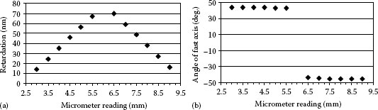
FIGURE 25.24 Accuracy test data at 157 nm using a Soleil-Babinet compensator: (a) retardation and (b) angle of fast axis.
Equations 25.24a and b give the correct values of magnitude and angle of fast axis of linear retardation in the range of 0 – π. When the actual retardation is between π and 2π, the polarimeter will still report a retardation value between 0 and π but an angle of fast axis shifted by 90°. This is because the Mueller matrices are identical for both linear retarders (δ, ρ) and (2π – δ, 90° + ρ). Consequently, this seemingly large error has no impact for optical systems that can be modeled by Mueller matrices.
The accuracy of this linear birefringence polarimeter was tested using a magnesium fluoride Soleil-Babinet compensator. This process involves simply measuring a dozen different retardation values in the range of 0–2π (λ, the measuring wavelength) and linearly fitting the data from 0−π (λ/2) to π–2π. Figure 25.24a and b displays the measured linear retardation and fast axis values, respectively, when the Soleil-Babinet compensator was dialed to successive settings at a regular interval. The retardation values shown in Figure 25.24a form a linear relationship in each half (Y = 21.217X – 49.599, R2 = 1.0000, and Y = −21.419X + 209.08, R2 = 1.0000). The linear-fit equations for the two halves give nearly identical slopes with opposite signs, which indicate correct calibration and proper alignment of the optical components in the polarimeter. Ideally, the linear fit lines of the measured retardation values in the first and second halves should intersect at exactly one half of the measuring wavelength (λ/2), or 78.8 nm, as compared to the measured values of 79.2 nm.
This is a simpler procedure than what was used to obtain Figure 25.17. The Soleil-Babinet compensator used here does not need to be calibrated. Simpler compensators such as a Babinet compensator can also be used with this procedure. This simple procedure can be repeated at other lithographic wavelengths and when the compensator is set at different angles. Table 25.3 summarizes the test results of a few experiments. The instrument is estimated to have an accuracy error of <1%. Furthermore, the error found by this simple process can be used to correct it if necessary.
25.4.1.5 Measuring Linear Birefringence at Different DUV Wavelengths
The DUV linear birefringence polarimeter provides at-wavelength (157, 193, and 248 nm) measurement for CaF2, fused silica, and other UV materials used in the optical lithography industry. A variety of CaF2 samples were measured at those three DUV wavelengths with the measuring light beam propagating along the [111] crystal axis. For comparison, the same samples were also measured on a 633 nm linear birefringence polarimeter. The birefringence maps for most of the CaF2 samples measured at 157 nm showed a similar pattern of fast axis angle and a higher linear retardation value when compared with the results measured at 633 nm. This is as expected from the dispersion of stress-birefringence with wavelengths.
However, a number of CaF2 samples exhibited little correlation in the maps of fast axis angle measured at 157 and 633 nm [80]. Those samples also gave very different maps of linear retardation value measured at 157 and 633 nm. One such example is shown in Figure 25.25a and d. The two linear retardation maps shown in Figure 25.25a and d for the same CaF2 sample are clearly different in both magnitude and angular patterns. The linear retardation maps measured at 193 and 248 nm are shown in Figure 25.25b and c for comparison. There is a gradual progression in the birefringence angular and magnitude patterns from 157 to 193, 248, and 633 nm.
TABLE 25.3
Accuracy Error of the DUV Polarimeter
a SBC, Soleil-Babinet compensator.
Since the photoelastic coefficient of a material depends on the wavelength, a given stress in a material will exhibit different values of linear retardation at different wavelengths. From this stress-birefringence dispersion, one would expect to observe different values of retardation when measuring the same sample at different wavelengths. However, stress-birefringence dispersion would not explain a change in the angle of fast axis measured at different wavelengths. After all, the fast axis of stress-birefringence is determined by the direction of the stress-force; this does not change with measuring wavelengths. There must be a different factor to explain the angular pattern changes shown in Figure 25.25a through d.
In addition to stress-birefringence, intrinsic birefringence is also a factor in CaF2, especially at short wavelengths. Intrinsic birefringence has an acute angular dependence in CaF2 [77,78]. While it is zero when a light beam propagates along the [111] crystal axis, the intrinsic birefringence reaches a maximum when a light beam propagates along the [110] crystal axis. A perfect CaF2 crystal has no intrinsic birefringence along the [111] axis. However, this would not be the case if a CaF2 sample has serious crystal defects where the crystal axis may vary significantly in different domains. When a low-quality [111] CaF2 sample is measured at 157 nm, variations in crystal axis can cause the intrinsic birefringence to contribute to the measured retardation.
When measured at 633 nm, intrinsic birefringence in CaF2 is negligible due to its sharp decrease at longer wavelengths. Therefore, the 633 nm linear retardation result shown in Figure 25.25d is entirely due to stress birefringence. However, when this sample is measured at 157 nm, there is an additional contribution to total linear retardation from intrinsic birefringence. This is caused by crystal axis “wandering” in poor quality CaF2 samples. X-ray imaging data of CaF2 samples with poor crystal quality supports this argument [81].
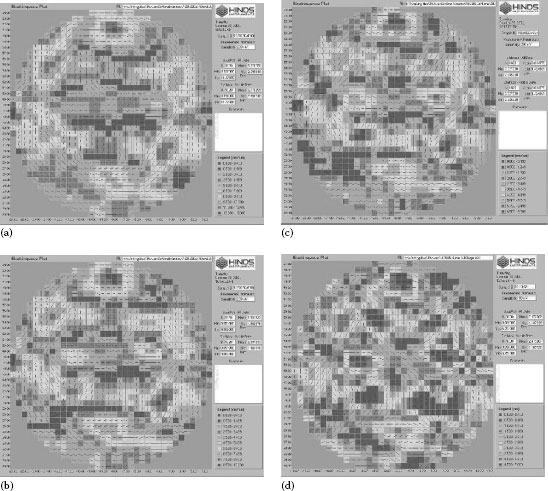
FIGURE 25.25 Linear retardation maps of a [111] CaF2 window measured at four wavelengths. (a) 157 nm (display scale for retardation: 0–15 nm; averaged retardation: 5.77 nm; number of data points: 1020); (b) 193 nm (display scale for retardation: 0–10 nm; averaged retardation: 3.89 nm; number of data points: 1020); (c) 248 nm (display scale for retardation: 0–8 nm; averaged retardation: 3.01 nm; number of data points: 1020); and (d) 633 nm (display scale for retardation: 0–7 nm; averaged retardation: 2.47 nm; number of data points: 1000).
25.4.1.6 DUV Polarimeter for Measuring Lenses
The DUV special polarimeter described earlier has fixed source and detector modules. It was designed to measure samples with parallel surfaces. To measure a lens, the polarimeter must fulfill several additional requirements.
A lens will bend a light beam by refraction. The detector module must first be moved to where the refracted beam is located after the lens and then be tilted normal to the refracted beam for polarization measurement. In addition, to model how a lens is used in an optical system, the incident angle of the measuring beam to the lens being tested will be controlled. Therefore, both the detector and source modules require linear and rotational controls.
Figure 25.26 shows an engineering diagram of the so-called Exicor OIA (oblique incident angle) birefringence measurement system, which is specifically designed for measuring lenses. In this system, the sample stage provides three degrees of freedom of motion. A lens under test can be moved in the horizontal plane (XY plane) with two stages allowing translation up to 500 mm in both X and Y axes. A lens sample can also be rotated by 360° in the XY plane during test. Additionally, each of the source module and detector module has two degrees of freedom of motion, translational in the X-axis up to 1250 mm and tilt from −50° to 50°. All motions are accurately controlled by a computer. The motion control allows us to measure residual birefringence in a lens at different incident angles. Note that all components inside each module remain fixed relative to one another.
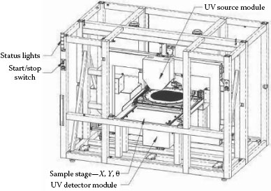
FIGURE 25.26 An engineering diagram of the Exicor OIA birefringence measurement system.
The light source used in this system provides a well-collimated beam from 190 to 800 nm. This instrument can provide birefringence mapping at fixed wavelengths, such as 193, 248, 365, 633 nm and any user defined wavelength from DUV to NIR. With an added option, the Exicor OIA system can also provide spectroscopic measurement from DUV to NIR at a fixed position on the sample.
We have measured several lenses at 193 nm using this system. One of them is an optical lithographic lens. The photo of this lens is shown in Figure 25.27a. There is a significant curvature on the top surface of this lens. The incident angles to the top surface of this lens were so chosen that the measuring beam after the refraction of the top surface is parallel to the vertical direction for all measurements. The measured residual birefringence map is shown in Figure 25.27b. Excluding the peripheral region, nearly all measured values of residual linear retardation for this lens are below 0.4 nm. This is a very high-quality lens with extremely low residual birefringence.
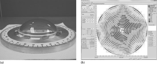
FIGURE 25.27 (a) A photo picture of a lithographic lens and (b) map of measured linear retardation values of the same lens with normal incidence to the top surface (measuring wavelength: 193 nm).
25.4.2 NEAR-NORMAL REFLECTION DUAL PEM POLARIMETER AND APPLICATIONS IN THE NUCLEAR FUEL INDUSTRY
Previously, I mentioned that Jellison championed the dual PEM design and applied it to measuring retardation and diattenuation properties of both transmissive and reflective samples. In this section, I describe one particular example of Jellison’s recent work.
Jellison and coworkers recently extended the 2-MGE to a two-modulator generalized ellip-sometry microscope (2-MGEM) [61,62,63]. The 2-MGEM instrument simultaneously measures eight elements of the Mueller matrix in near-normal reflection mode with 4-μm spatial resolution. One of the applications of the 2-MGEM is to measure the linear diattenuation of the pyrocarbon layers in the cross-section of TRistructural-ISOtropic (TRISO) nuclear fuel particles [63]. Traditionally, the nuclear industry has measured the OPTical Anisotropy Factor (OPTAF), which is related to the linear diattenuation (defined as N in Refs. [58,59,60,61,62,63]), where OPTAF = Rmax/Rmin = (1 + Ld)/(1 – Ld).
TRISO nuclear fuel is used in many of the fourth-generation nuclear power reactor designs, such as the advanced gas reactor (AGR). Each TRISO particle is ~1 mm in diameter and contains a kernel of radioactive material and four layers designed to contain the radioactive material during irradiation. The four layers are (1) a buffer layer, consisting of porous carbon, (2) an inner pyrocarbon layer (IPyC), (3) a silicon carbide (SiC) layer for structural integrity, and (4) an outer pyrocarbon layer. The optical anisotropy (expressed either as the OPTAF or the linear diattenuation) of the two pyrocarbon layers is a critical quality control factor, which can be accurately measured by the 2-MGEM. Furthermore, the 2-MGEM provides a “map” of the diattenuation over the entire TRISO particle cross-section, making enhanced characterization possible.
This 2-MGEM OPTAF system was commercialized in 2007 through a collaboration between Oak Ridge National Laboratory and Hinds Instruments, Inc. Two commercial systems have been built so far. Figure 25.28a shows the reflected light intensity of a TRISO nuclear fuel particle obtained using this system, while Figure 25.28b shows the magnitude of the diattenuation N for the same particle. The kernel (containing the nuclear material) has been removed and replaced with potting epoxy. Clearly, the IPyC and OPyC layers show significant diattenuation, while the other layers do not. Other results are shown in Refs. [61,62,63].
Comparisons between measurements taken on the system at Oak Ridge and the commercial version obtain nearly identical results, as do measurements taken on the same samples at different times. Therefore, the 2-MGEM system provides reproducible data that is useful for the quality assurance requirements of the nuclear fuel industry. It is my hope that scientists and engineers within the nuclear fuel industry can read the diattenuation data and decipher the quality control information to improve the performance of TRISO fuel particles.
25.4.3 SPECIAL POLARIMETERS FOR THE FPD INDUSTRY
The liquid crystal display (LCD) has become the dominant FPD technology in consumer electronics, including digital cameras, cell phones, PC monitors, and TVs. Since an LCD depends on the birefringence properties of an LC material to achieve its display functions, the birefringence properties are critical to performance for all key optical components used in an LCD. Consequently, special polarimeters have been developed for a variety of applications in the LCD industry.
25.4.3.1 Measuring Glass Substrate
The glass substrate of an LCD is usually thinner than 1 mm. The linear retardation is typically below 1 nm in high-quality LCD glass substrates. The PEM linear birefringence polarimeter, which serves the optical lithography industry well with its high sensitivity, is also suited to measuring the stress birefringence (and stress) in LCD glass substrates.
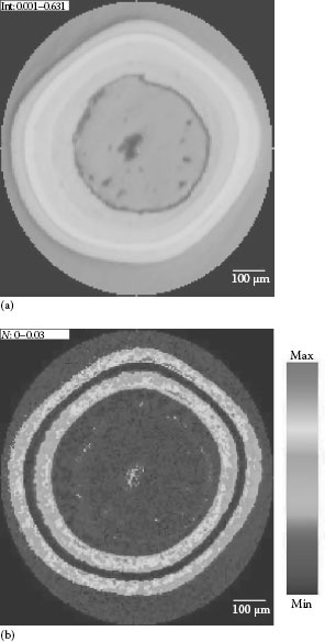
FIGURE 25.28 (a) Grayscale image of the reflected light intensity; (b) a map of the linear diattenuation from a cross-section of a TRISO nuclear fuel particle. Notice that the outmost layer shown was an epoxy layer introduced when making the cross-section of the TRISO particle.
25.4.3.2 Measuring LCD-FPD Components at RGB Wavelengths
The LCD-FPD industry also requires at-wavelength measurement. For this industry, the wavelengths are red, green, and blue (RGB). One way to build an RGB linear birefringence polarimeter is to use a Hg–Xe lamp as the light source. This source emits strong peaks at both blue and green wavelengths in addition to the broad spectral irradiation in the visible spectrum [82]. The strong blue and green mercury emissions improve the accuracy and sensitivity of measurements at those wavelengths. Other light sources include LEDs, fluorescent lamps, lasers, and black-body thermal light sources.
Figure 25.29 shows the linear retardation maps of a stretched polymer film measured at the blue, green, and red wavelengths. The same retardation pattern was observed at all three wavelengths. The average retardation values measured at RGB increase from 8.38 to 8.66 nm and 9.33 nm, respectively, as expected due to the birefringence dispersion of this polymer film sample.
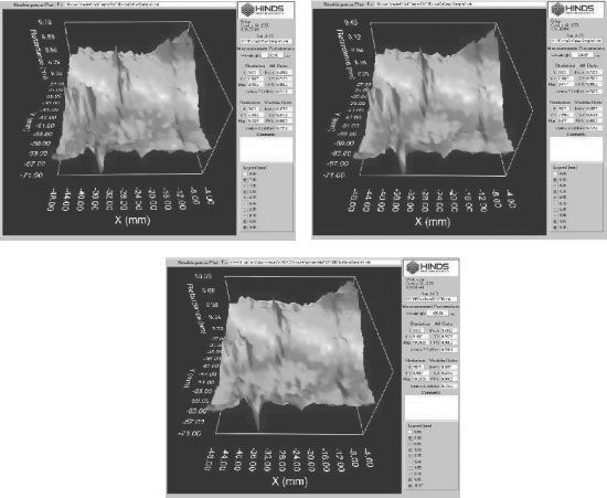
FIGURE 25.29 Retardation maps of a stretched polymer film sample measured at top middle, and bottom wavelengths.
An advantage of the RGB polarimeter described earlier is that it eliminates possible interference effects resulting from the use of a coherent laser to measure thin films. It is true that many of the film samples I have measured exhibit little laser interference. However, strong laser interference has been observed in some thin film samples. Two examples, one with and the other without laser interference effect, are shown in Figures 25.30 and 25.31.
Figure 25.30a and b displays the linear retardation maps of the same thin film sample measured on the RGB polarimeter and a polarimeter using a He–Ne gas laser, respectively. The averaged retardation values for those two measurements are in good agreement (6.29 and 6.21 nm). The retardation patterns displayed in Figure 25.30a and b are very similar. One visual difference between the two maps is their spatial resolutions. Namely, Figure 25.30b exhibits a higher spatial resolution than Figure 25.30a does, but that is caused by the smaller beam size of the laser used. This thin film sample exhibits no observable laser interference.
Figure 25.31a and b illustrates an example with significant laser interference. Figure 25.31a and b displays the linear retardation maps of a thin film sample measured on the RGB polarimeter and a He–Ne gas laser polarimeter, respectively. Although the averaged retardation values for those two measurements are in good agreement (10.89 and 10.81 nm), the retardation pattern depicted in Figure 25.30b clearly shows laser interference. It is, therefore, advantageous to use a noncoherent light source in a polarimeter for thin film applications.
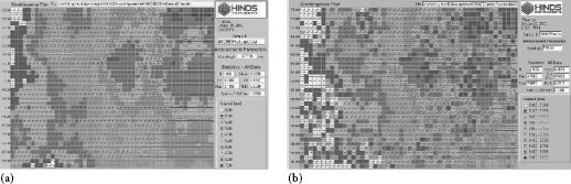
FIGURE 25.30 Linear retardation maps of a thin film sample measured on (a) the RGB polarimeter and (b) a polarimeter using a He–Ne gas laser.
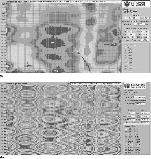
FIGURE 25.31 Linear retardation maps of a thin film sample measured on (a) the RGB polarimeter and (b) a polarimeter using a He–Ne gas laser, showing laser interference effect.
25.4.3.3 Measuring Retardation Compensation Films at Normal and Oblique Angles
Retardation compensation films are key optical components used in the LCD to improve the viewing angle. Different types of sophisticated compensation films have been developed recently, including biaxially stretched polymers, discotic compensation films, and photo-aligned anisotropic films [83,84,85,86]. Ideally, a compensation film should have uniform in-plane retardation and a well-defined pattern for out-of-plane (vertical) retardation. The retardation value and uniformity in a compensation film directly affect the performance of an LCD at normal and oblique viewing angles. A polarimeter is required to provide both in-plane and out-of-plane measurements for these films.
A polarimeter using a tilt stage can provide retardation measurements at normal and different oblique incident angles. A typical set of data is shown in Figure 25.32a for a compensation film measured at different incident angles [87]. This compensation film has an in-plane retardation value of ~14 nm. To avoid complicated additions of in-plane and out-of-plane linear retardation, the sample was oriented so that the fast axes of both the normal and oblique retardations were approximately aligned to 0°. Figure 25.32a and b shows the measured retardation and angles of fast axis in the tilt range from −50° to 50° in 5° increments. The pattern of oblique retardation with tilt angle is used to calculate vertical birefringence, traditionally the ((Rth = |nZ −((nX + nY)/2)| d)) parameter, and ultimately to improve the viewing angle in LCD designs.
25.4.3.4 Measuring Retardation at a Fast Speed
For LCD-FPD industrial applications, birefringence polarimeters should be able to operate in two modes. In a so-called Lab mode, PC-controlled XY linear stages provide precise motion control to accurately map the birefringence property of a sample. This is an “off-line” application, and a data collection rate of several measurements per second is usually sufficient. In the “Lab” mode, precise motion control may consume most of the time in a measurement cycle. In a so-called Fab mode, sample movement is normally handled in a production process. The speed of a fast moving sample demands a fast data collection rate. An “in-line” application such as this is typically involved in monitoring the quality of polymer films or thin glass sheets in production. In the “Fab” (semiconductor fabrication plant) mode, a PEM-based polarimeter, with fast modulation of the PEM (tens of kHz), easily affords a rate of over 100 data points per second.
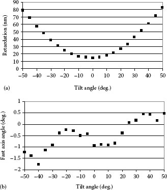
FIGURE 25.32 Birefringence data measured at normal and different oblique angles of a stretched polymer film: (a) oblique retardation values and (b) angles of fast axis.
To simulate an in-line film monitoring process in our laboratory, we made a motor-driven rolling loop using a polymer film [88]. In this experiment, the polarimetric function was separated from the mechanical function of moving the polymer film. Figure 25.33a and b shows the repeatable patterns of retardation magnitude and angle of fast axis measured in two rolling cycles. The sampling rate for the experiment was ~140 data points per second.
The PEM-based special polarimeter gives a distinctive advantage in the “Fab” mode operation over other polarization modulation methods. The superior optical properties of the PEM deliver polarimetric measurements characterized by high sensitivity and accuracy. At the same time, the fast modulation frequency of the PEM (tens of kHz) furnishes a sampling rate of hundreds of data points per second. For an “in-line” application, polarimeters using rotating polarizers or wave plates are too slow. Electro-optic modulators can modulate very fast, but they do not provide sufficient sensitivity for many polarimetric measurements. A PEM-based special polarimeter affords both high sensitivity and fast data collection, and thus, it is best suited to “in-line” monitoring of glass sheet and thin film productions.
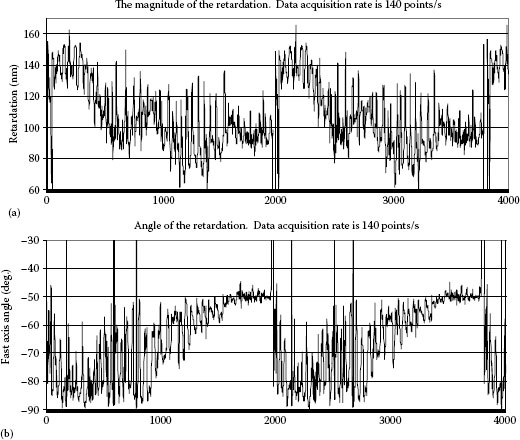
FIGURE 25.33 (a) Retardation magnitude and (b) angle of fast axis measured in two rolling cycles.
25.4.4 SPECIAL POLARIMETERS FOR CHEMICAL, BIOCHEMICAL, AND PHARMACEUTICAL APPLICATIONS
In chemical, biochemical, and pharmaceutical applications, a polarimeter is primarily used to characterize chiral molecules. A molecule is chiral when it cannot be superimposed with its mirror image. Since many molecules in the bodies of human beings and animals, including amino acids and proteins, are chiral, most drugs used to treat diseases are also chiral. The chiral branches of the chemistry, biochemistry, and pharmaceutical industries are critical to the health of living beings.
For a chiral molecule, the two nonsuperimposable mirror images are called enantiomers. Under normal conditions, enantiomers have identical physical and chemical properties, except for how they interact with circularly polarized light. Polarimetry is the key optical means for distinguishing between enantiomers and studying chiral molecules. It is beyond the scope of this chapter to discuss chiral molecule applications in detail. However, I will briefly introduce three major types of polarimeters used in chemical, biochemical, and pharmaceutical applications. Interested readers are referred to a collection of articles in natural optical activity [89].
25.4.4.1 Circular Dichroism Spectrometer
A CD spectrometer measures the differential absorption of a chiral sample between left and right circularly polarized light (ΔA = AL – AR). The CD signals of a chiral sample are usually very small. It is impossible to determine a typical CD signal by measuring AL and AR separately and then calculating the difference. High-quality polarization modulation must be used in a CD spectrometer. Although there are different types of polarization modulators, all modern CD spectrometers use the PEM due to its superior optical properties.
In a CD spectrometer, the polarization modulation module contains a polarizer followed by a PEM where the optical axes of the two components are 45° apart. The sample is placed between the PEM and the detector. Note that there is no analyzer in front of the detector in a CD spectrometer. The PEM is set to modulate between left and right circularly polarized light. When a sample exhibits no differential absorption between left and right circularly polarized light, the detector receives a constant light intensity with no modulated signal. When a chiral sample absorbs left and right circularly polarized light differently, the detector will receive a modulated CD signal.
CD spectrometers are common in UV–vis, near IR, and mid-IR spectral regions. In academic research, CD spectrometers are primarily used to extract different levels of molecular structural information about the molecule and its interactions with other molecules. In industrial applications, CD spectrometers are often used to detect the concentration of a desired enantiomer or the enantiomeric excess of a chiral compound. CD spectrometers in both UV–vis and IR spectral regions have been commercially available for decades from a number of manufacturers.
25.4.4.2 Optical Rotation Polarimeter
Optical rotation is also called circular birefringence. An optical rotation polarimeter measures the rotation of the polarization plane of a linearly polarized light beam when it passes through a chiral sample. The simplest optical rotation polarimeter is constructed by using a polarizer and a crossed analyzer. The optical rotation is the angular difference in the null positions on the analyzer with and without a chiral sample. Simple optical rotation polarimeters have been used in the sugar industry for nearly two centuries. An optical rotation polarimeter is perhaps the most commonly used special polarimeter in industrial and analytical laboratories. In fact, when people use the term “polarimeter,” most refer to an optical rotation polarimeter.
When a PEM is used in an optical rotation polarimeter, the polarization modulation module may contain a polarizer at 0°, a PEM at 0° and an analyzer at 45°. The sample can be placed between the polarizer and the PEM. When there is no optical rotation, the detector receives no modulated signal, because the polarizer and the optical axis of the PEM are parallel to each other. When the sample rotates the polarization plane away from 0°, the detector will receive a modulated signal at the second harmonic of the PEM. The PEM-based optical rotation polarimeter provides high sensitivity.
25.4.4.3 Polarization Analyzer for Fluorescence and Scattering
Fluorescence and light scattering from chemical and biochemical molecules contains polarization information that is useful in studying the properties and chemical dynamics of the molecules. While the chemical and biochemical processes can be complicated, the polarimetric applications are similar to what has been described in previous sections. A special Stokes polarimeter using a single PEM, as shown in Figure 25.3, is often sufficient to measure the polarization state of the fluoresced or scattered light beam, although complete Stokes and Mueller polarimeters are used for some applications.
25.4.5 STRESS BIREFRINGENCE POLARIMETER FOR SI USED IN THE SOLAR PHOTOVOLTAIC INDUSTRY
Silicon (Si)-based solar cell technology dominates the commercial photovoltaic (PV) market. Controlling the cost of Si material is one of the most significant factors in the production of Si solar panels. Material losses occur throughout the manufacturing process, mostly due to stress and defects that arise from the crystal growth process. Stress in Si crystals can remain undetected long into the fabrication process, until ultimately the end product (finished cell) fails, or its performance is severely compromised. Measuring stress in Si components can improve the yield of high-quality solar panels.
Several models of birefringence polarimeter using the Exicor technology are available to measure stress in Si components used in producing solar panels. A special polarimeter as described in Section 25.4.1 using NIR light source and detector can be used to map the stress in solar wafers and other samples (<160 mm × 160 mm). A modular polarimeter as described in Section 25.4.3.4 can be adopted to NIR for in-line measurement of stress in Si wafers at a high speed. A birefringence polarimeter with large stages can be used to measure stress in large Si ingots. It is advantageous to measure stress in Si ingots early in the production process so that low-quality segments in an Si ingot can be identified before sawing them into wafers, thus avoiding the subsequent processing costs incurred in the solar cell fabrication process. Figure 25.34 illustrates an example of stress measurement in a squared monocrystal Si ingot [96].
The test segment of an Si ingot was cut from p-type Czochralski (CZ)-grown Si crystals. The as-grown ingot was shaped into 156 mm × 156 mm pseudosquares. The surfaces of the squared ingot were finished using a grinding process. The Si ingot was measured with the measuring beam parallel to the [100] crystal direction. To calculate stress from measured linear retardation, we use the stress-optic law
where
σ is the differential stress (in MPa; 106 pascal)
δ is the linear retardation (in nm)
t is the thickness of the sample (in mm)
CB is the stress-optical constant (in Brewsters or 10−12 Pa−1; CB = 24 for Si(100) as an average of four reported values) [97]
Figure 25.34a depicts the 2D retardation map for a unique segment of an Si ingot (about 310 mm in length). The false color retardation image indicates multiple orders of retardation along the crystal growth direction of the ingot. Figure 25.34b and c illustrates, respectively, the measured raw retardation and calculated stress values for a line of data in the middle of the 2D map.
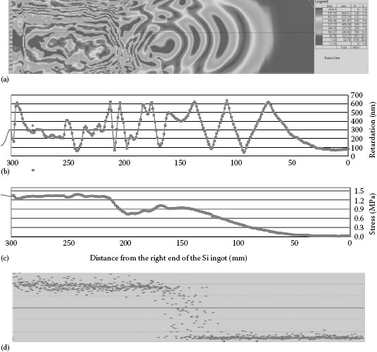
FIGURE 25.34 (a) 2D linear retardation map of stressed Si ingot; (b) line data for measured linear retardation (The right end of the Si ingot is labeled “0” on the horizontal axis. Each data point represents a 1 mm spacing.); (c) calculated stress; and (d) bowing of Si wafers produced from the same ingot.
Moving in the crystal growth direction from right to left, the 2D map starts with retardation values that are low and uniform, increases significantly and continuously as concave-curved striation patterns form, and finally develops into more complicated patterns of multiple orders of retardation. The appearance of the pronounced concave-shaped pattern and its evolution to a rather complex stress distribution indicate enhanced defect densities due to radial stress relaxation toward the outside.
Shown in Figure 25.34b and c, from right to left, the measured raw retardation values start low, which correspond to a very low level of stress (≤0.1 MPa) for the first 50 mm in length from the right end of the Si ingot. The measured raw retardation values then go through several peak-to-valley cycles until 210 mm from the end (right side) of the Si ingot. Using the measured angles of fast axis, we can convert the measured raw retardation values to corrected retardation values, then to stress in MPa. As seen in Figure 25.34c, the stress increases almost continuously from 0.1 MPa at 50 mm (from the right end of the Si ingot) to about 1.4 MPa at 210 mm. The stress remains fairly constant around 1.4 MPa beyond 210 mm for the left-end segment of the Si ingot.
We have sliced this ingot into 200 μm (thickness) wafers. Figure 25.34d shows the average bow of these wafers with respect to their axial position in the crystal. We can clearly see a correlation between the levels of stress in the Si ingot and the magnitudes of bowing in the wafers sliced from that ingot. The results shown in Figure 25.34 suggest that stress above 0.5 MPa in monocrystal Si ingots could result in strong wafer bow, thus severely lowering the quality of a wafer.
25.4.6 PEM–CAMERA IMAGING POLARIMETER
As previously mentioned, the main challenge to employing PEMs in a camera-based imaging instrument is that CCD or CMOS (complementary metal–oxide–semiconductor) cameras have a much slower readout rate than the modulation frequency of a PEM (tens of kHz), such that the specific polarization information carried on the modulation frequency of the PEM will be averaged out. Generally speaking, there are three basic approaches to overcome this challenge: slowing down the modulation, pulsing the light source, and gating the camera according to the modulation of the PEM.
The first approach is to slow down polarization modulation using the beat frequency of two PEMs. This approach, developed by Diner et al. [41,42], is briefly described in Section 25.2.2.
The second approach is to periodically expose, or gate, the camera in synchronization with the modulation of the PEM. Masking selected rows of the CCD according to the modulation of the PEM, which was developed by the ETH Zurich group [37,38,39,40], is one such example. This second approach is also briefly described in Section 25.2.2.
With today’s CCD and CMOS technologies, gating the camera becomes easier. For example, an intensified CCD (ICCD) camera has an image intensifier that can act as both a fast (nanoseconds) optical shutter and a signal amplifier [98]. Such an ICCD may be directly used in a PEM–camera polarimeter, with the reference signal of the PEM triggering the intensifier. Lack of industrial applications and the high cost of ICCD cameras may be the primary reasons for not having a commercially available PEM–ICCD polarimeter. In addition to ICCD, Vitkin and coworkers used field programmable gate array (FPGA) to trigger the camera according to the relative phase of two PEMs [99]. Subsequently, the same group has extended the FPGA triggering method to a complete Mueller polarimeter using four PEMs [100].
The third approach is to generate short pulses of a light source in synchronization with the modulation frequency of a PEM (so-called stroboscopic illumination) so that the camera only receives light pulses carrying specific polarization information. Gleyzes, Boccara, and Saint-Jalmes used this approach in 1997 to build an imaging interferometer by integrating a PEM into a commercial microscope [101]. Dubois, Boccara, and coworkers subsequently developed a full-field microscope for optical coherence tomography (OCT) applications using stroboscopic illumination where an infrared LED was pulsed at four specific phases during a modulation cycle of the PEM [102]. Chao and coworkers further applied stroboscopic illumination to PEM imaging ellipsometry [103,104,105].
In our laboratory, we have built several PEM–camera imaging polarimeters using stroboscopic illumination. In one of the PEM–camera imaging polarimeters, we use a green (530 nm) LED array that is pulsed according to the modulation phases of two PEMs. The field of view of this polarimeter is about 60 mm × 60 mm. Figure 25.35 displays the measured linear retardation images of a plastic ruler and a quartz wedge coupled to a matching fused silica wedge.
The quartz wedge provides linearly varying retardation values in the horizontal direction. Since we use a 530 nm light source, this PEM–camera imaging polarimeter has an upper measurement limit of 265 nm. Consequently, the reported retardation values show a saw-tooth pattern with peaks (265 nm) and valleys (0 nm) along the horizontal direction of the quartz wedge. In Figure 25.35c, a single row of data from the image shown in Figure 25.35a is plotted to exhibit the saw-tooth pattern more clearly. Note that the good linearity of measured retardation values between 0 and 265 nm is an indication of the good accuracy of this PEM imaging polarimeter. Furthermore, the measured angles of fast axis switch 90° in every peak or valley cycle as shown in Figure 25.35b. As is well known, using two or more wavelengths in the measurements can resolve multiple orders of retardation.
The plastic ruler was a poor choice of sample in terms of industrial application. We have measured many cell phone panels (one example of an outdated cell phone panel is shown in Figure 25.35d), waveplates, and special wafers that are more relevant to industrial applications. However, I particularly like this plastic ruler, because it has a large variation of retardation, it directly displays the field size, and its image indicates how effectively the algorithm eliminates certain measurement artifacts.
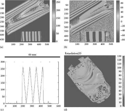
FIGURE 25.35 Measured retardation images of a mid-field PEM imaging polarimeter. (a) and (b) retardation magnitude and angle images of a plastic ruler and a quartz wedge; (c) a single row of data from image (Figure 25.35a); (d) retardation image of a cell phone panel.
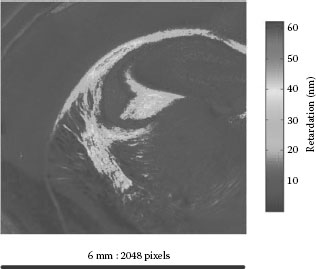
FIGURE 25.36 Preliminary retardation image of a slice of mouse brain. (The tissue section is a courtesy of S. Segal, Saint Louis University School of Medicine, St. Louis, MO.)
Another PEM–camera system that we built in our laboratory is a microscopic polarimeter. This polarimeter contains a simple, home-made microscope with a low magnification (2× or 5×) objective, two PEMs, a modest resolution (4 megapixels) camera, and an FPGA-triggered LED light source. This particular device has proven effective in resolving birefringence found in biological specimens. One such birefringent substance is myelin, which is a lipoprotein found in the nervous system, particularly in the white matter. Myelin wraps around the elongated part of neuronal cells known as axons, forming cable-like structures coated with an insulating (myelinated) cuff. Axons (also termed fibers) tend to form thicker bundles with millions of myelinated axonal fibers known as white matter tracts. White matter tracts containing myelin are characteristically birefringent. Since other parts of the brain tissue are not as rich in myelin as the white matter tracts, there is significant contrast between myelinated and nonmyelinated brain tissue in birefringence imaging [106]. The demonstration of the white matter tracts birefringence at cross section (thickness = 100 μm) in a sample from the mouse brain is shown in Figure 25.36.
Our goal is to provide a series of polarization imaging tools to research communities and industrial applications.
1. http://dictionary.webster.us/polarimetry; Webster’s Revised Unabridged Dictionary, 1913.
2. R. A. Chipman, Polarimetry, in Handbook of Optics I, 3rd edn., M. Bass, editor in chief, McGraw-Hill, New York, Chapter 15, 2010.
3. D. H. Goldstein, D. B. Chenault et al., Polarization: Measurement, analysis, and remote sensing I–XI, Proc. SPIE from 1997 to 2014.
4. R. M. A. Azzam, Optical polarimetry: Instrumentation and applications, Proc. SPIE 112 (1977).
5. H. Mott and W. -M. Boerner, Radar polarimetry, Proc. SPIE 1748 (1994).
6. A. Adamson, C. Aspin, C. J. Davis, and T. Fujiyoshi, Astronomical polarimetry: Current status and future directions, ASP Conference Series 343 (2005).
7. S. Fineschi, Polarimetry in astronomy, Proc. SPIE 4843 (2003).
8. R. M. A. Azzam and N. M. Bashara, Ellipsometry and Polarized Light, North-Holland, Amsterdam, the Netherlands, reprinted 1989.
9. D. H. Goldstein Polarized Light, 3rd edn., Taylor & Francis, New York, 2010.
10. J. Tinbergen, Astronomical Polarimetry, Cambridge University Press, Cambridge, MA, 2005.
11. J. Schellman and H. P. Jensen, Chem. Rev. 87, 1359 (1987).
12. S.-M. F. Nee, Polarization measurement, in The Measurement, Instrumentation and Sensors Handbook, J. G. Webster, ed., CRC Press, Boca Raton, FL, 1999.
13. P. S. Hauge, Surf. Sci. 96, 108 (1980).
14. J. M. Bueno, J. Opt. A: Pure Appl. Opt. 2, 216 (2000).
15. J. S. Tyo, D. H. Goldstein, D. B. Chenault, and J. A. Shaw, Appl. Opt. 45, 5453 (2006).
16. C. U. Keller, Instrumentation for astrophysical spectropolarimetry, in Astrophysical Spectropolarimetry, J. Trujillo-Bueno, F. Moreno-Insertis, and F. Sanchez, eds., Cambridge University Press, Cambridge, MA, 2002.
17. J. C. Kemp, J. Opt. Sci. Am. 59, 950 (1969).
19. G. G. Stokes, Trans. Camb. Philos. Soc. 9, 399 (1852).
20. D. S. Kliger, J. W. Lewis, and C. E. Randall, Polarized Light in Optics and Spectroscopy, Academic Press, San Diego, CA, 1990.
21. C. Brosseau, Fundamentals of Polarized Light—A Statistical Optics Approach, John Wiley & Sons, New York, 1998.
22. W. A. Shurcliff, Polarized Light: Production and Use, Harvard University Press, Cambridge, MA, 1962.
23. R. Clark Jones, J. Opt. Soc. Am. 31, 488; 493; 500 (1941); 32, 486 (1942).
24. H. Mueller, J. Opt. Soc. Am. 38, 661 (1948).
25. P. S. Theocaris and E. E. Gdoutos, Matrix Theory of Photoelasticity, Springer-Verlag, Berlin, Germany, 1979.
26. R. P. Feynman, R. B. Leighton, and M. Sands, The Feynman’s Lectures on Physics, Vol. I, p. 3202, Addison-Wesley Publishing, Menlo Park, CA, 1977.
27. D. Brewster, Philos. Trans. 106, 156 (1816).
28. M. Billardon and J. Badoz, C. R. Acad. Bc. Paris Ser. B 262, 1672 (1966).
29. L. F. Mollenauer, D. Downie, H. Engstrom, and W. B. Grant, Appl. Opt. 8, 661 (1969).
30. S. N. Jasperson and S. E. Schnatterly, Rev. Sci. Instrum. 40, 761 (1969); Errata 41, 152 (1970).
31. J. C. Kemp, US Patent No. 3,867,014 (1975).
32. B. Wang and J. List, Proc. SPIE 5888, 436 (2005).
33. J. C. Kemp, J. B. Swedlund, and B. D. Evans, Phys. Rev. Lett. 24, 1211 (1970).
34. J. C. Kemp, R. D. Wolstencroft, and J. B. Swedlund, Astrophys. J. 177, 177 (1972).
35. J. C. Kemp, G. D. Henson, C. T. Steiner, and E. R. Powell, Nature 326, 270 (1987).
36. J. C. Kemp, Proc. SPIE 307, 83 (1981).
37. J. O. Stenflo and H. Povel, Appl. Opt. 24, 3893 (1985).
38. H. P. Povel, C. U. Keller, and A. Yadigaroglu, Appl. Opt. 33, 4254 (1994).
39. A. M. Gandorfer and H. P. Povel, Astron. Astrophys. 328, 381 (1997).
40. A. M. Gandorfer, H. P. Povel, P. Steiner, F. Aebersold, U. Egger, A. Feller, D. Gisler, S. Hagenbach, and J. O. Stenflo, Astron. Astrophys. 422, 703 (2004).
41. D. J. Diner, A. Davis, B. Hancock, G. Gutt, R. A. Chipman, and B. Cairns, Appl. Opt. 46, 8428 (2007).
42. D. J. Diner, A. Davis, B. Hancock, S. Geier, B. Rheingans, V. Jovanovic, M. Bull, D. M. Rider, R. A. Chipman, A. -B. Mahler, and S. C. McClain, Appl. Opt. 49, 2929–2946 (2010).
43. J. O. Stenflo, Mem. S. A. It. 78, 181 (2007).
44. J. O. Stenflo, Rev. Mod. Astron. 17, 269 (2004).
45. S. S. Varnum, US Patent No. 5,744,721 (1998).
46. G. R. Boyer, B. F. Lamouroux, and B. S. Prade, Appl. Opt. 18, 1217 (1979).
47. B. Wang, J. List, and R. R. Rockwell, Proc. SPIE 4819, 1 (2002).
48. http://en.wikipedia.org/wiki/Tokamak.
49. www.tokamak.info.
50. F. M. Levinton, R. J. Fonck, G. M. Gammel, R. Kaita, H. W. Kugel, E. T. Powell, and D. W. Roberts, Phys. Rev. Lett. 63, 2060 (1989).
51. F. M. Levinton, G. M. Gammel, R. Kaita, H. W. Kugel, and D. W. Roberts, Rev. Sci. Instrum. 61, 2914 (1990).
52. D. Wroblewski and L. L. Lao, Rev. Sci. Instrum. 63, 5140 (1992).
53. H. Friedrich, Theoretical Atomic Physics, Springer-Verlag, Berlin, Germany, 1990.
54. B. Wang, R. R. Rockwell, and A. Leadbetter, Proc. SPIE 5888, 33 (2005).
55. R. M. A. Azzam, Opt. Lett. 2, 148 (1977).
56. D. H. Goldstein and R. A. Chipman, J. Opt. Soc. Am. A 7, 693 (1990).
57. M. H. Smith, Appl. Opt. 41, 2488 (2002).
58. G. E. Jellison Jr. and F. A. Modine, Appl. Opt. 36, 8184; 8190 (1997).
59. G. E. Jellison Jr. and F. A. Modine, US Patent No. 5,956,147 (1999).
60. G. E. Jellison Jr., C. O. Griffiths, D. E. Holcomb, and C. M. Rouleau, Appl. Opt. 41, 6555 (2002).
61. G. E. Jellison Jr., D. E. Holcomb, J. D. Hunn, C. M. Rouleau, and G. W. Wright, Appl. Surf. Sci. 253, 47 (2006).
62. G. E. Jellison Jr., J. D. Hunn, and C. M. Rouleau, Appl. Opt. 45, 5479–5488 (2006).
63. G. E. Jellison Jr., J. D. Hunn, and R. A. Lowden, J. Nucl. Mater. 352, 6 (2006).
64. R. C. Thompson, J. R. Bottiger, and E. S. Fry, Appl. Opt. 19, 1323 (1980).
65. R. A. Chipman, Proc. SPIE 6682, 66820I-1 (2007).
66. B. Wang and T. C. Oakberg, Rev. Sci. Instrum. 70, 3847 (1999).
67. B. Wang, T. C. Oakberg, and P. Kadlec, US Patent No. 6,473,179 (2002).
68. B. Wang, T. C. Oakberg, and P. Kadlec, US Patent No. 6,697,157 (2004).
69. B. Wang, Proc. SPIE 4103, 12 (2000).
70. B. Wang and W. Hellman, Rev. Sci. Instrum. 72, 4066 (2001).
71. G. E. Moore, Electronics, 38(8), 114–117 (April 19, 1965).
72. B. Wang and P. M. Troccolo, Proc. SPIE 3873, 544 (1999).
73. B. Wang, J. Microlith. Microfab. Microsyst. 1, 43 (2002).
74. H. J. Levinson and W. H. Arnold, in Handbook of Microlithography, Micromachining, & Microfabrication, Vol. 1, P. Rai-Choudhury, ed., IET, Chapter 1, pp. 11–138, 1997.
75. D. M. Williamson, US Patent No. 5,537,260 (1996).
76. E. Hecht and A. Zajac, Optics, Addison-Wesley, London, U.K., p. 251, 1974.
77. J. H. Burnett, Z. H. Levine, E. L. Shirley, and J. H. Bruning, J. Microlith. Microfab. Microsys. 1, 213 (2002).
78. J. H. Burnett, Z. H. Levine, and E. L. Shirley, Phys. Rev. B 64, 241102(R) (2001).
79. B. Wang, C. O. Griffiths, R. Rockwell, J. List, and D. Mark, Proc. SPIE 5192, 7 (2003).
80. B. Wang, R. Rockwell, and J. List, J. Microlith. Microfab. Microsyst. 3, 115 (2003).
81. B. Wang and W. Rosch, Proc. SPIE 6682, 36 (2007).
82. B. Wang, A. Leadbetter, R. R. Rockwell, and D. Mark, Proc. IDRC 26, P4 (2006).
83. H. Mori and P. J. Bos, Jpn. J. Appl. Phys. 38, 2837 (1999).
84. H. Mori, Y. Itoh, Y. Nishiura, T. Nakamura, and Y. Shinagawa, Jpn. J. Appl. Phys. 36, 143 (1997).
85. T. Ishikawa, J. F. Elman, and D. M. Teegarden, US Patent No. 7,236,221 (2007).
86. K.-H. Kim, Y. Jang, and J.-K. Song, US Patent No. 7,321,411 (2008).
87. B. Wang and J. List, SID Digest, P55 (2004).
88. B. Wang, R. R. Rockwell, and A. Leadbetter, Proc. SPIE 5531, 367 (2004).
89. A. Lakhtakia, ed., Selected papers on natural optical activity, SPIE Milestone Series, Vol. MS 15, B. J. Thompson, General ed., SPIE, 1990.
90. L. Hirschy, B. Wang, J. Wolf, R. Lakanen, and B. Hartmann, Proc. SPIE 8486, 848619 (2012).
91. B. Wang and A. Leadbetter, Proc. SPIE 7853, 78530C (2010).
92. B. Wang, W. B. Sparks, T. A. Germer, and A. Leadbetter, Proc. SPIE 7441, 744108 (2009).
93. W. B. Sparks, J. Hough, T. A. Germer, F. Chen, S. DasSarma, P. DasSarma, F. T. Robb et al., Proc. Natl. Acad. Sci. USA 106, 7816–7821 (2009).
94. W. B. Sparks, J. Hough, L. Kolokolova, T. A. Germer, F. Chen, S. DasSarma, P. DasSarma et al., JQSRT 110, 1771–1779 (2009).
95. O. Arteaga, J. H. Freudenthal, B. Wang, and B. Kahr, Appl. Opt. 51, 6805 (2012).
96. B. Wang, A. Leadbetter, and B. Seipel, Energy Procedia 38, 959–967 (2013).
97. V. Ganapati et al., J. Appl. Phys. 108, 063528 (2010).
98. For example, iStar gated ICCD from Andor Technology, www.andor.com.
99. S. Alali, T. Yang, and I. Alex Vitkin, Opt. Lett. 38 (16), 2997–3000 (2013).
100. S. Alali and I. A. Vitkin, Opt. Eng. 52(10), 103114 (2013).
101. P. Gleyzes, A. C. Boccara, and H. Saint-Jalmes, Opt. Lett. 22(20), 1529 (1997).
102. A. Dubois, L. Vabre, A.-C. Boccara, and E. Beaurepaire, Appl. Opt. 41(4), 805–812 (2002).
103. C. Y. Han and Y. F. Chao, Rev. Sci. Instrum. 77, 023107 (2006).
104. H. M. Tsai and Y. F. Chao, Opt. Lett. 34 (15), 2279–2281 (2009).
105. H. M. Tsai, C. W. Chen, T. H. Tsai, and Y. F. Chao, Rev. Sci. Instrum. 82, 035117 1-5 (2011).
106. Segal, S. (2013). Personal communication.