CONTENTS
28.3 Some Typical Filters and Their Design Principles
28.3.2 High Reflection Coating
28.3.3 Long-Wave Pass and Short-Wave Pass Filters
28.3.5 Band-Stop Filter (Rugate Filter)
28.5 Characterization of a Coated Film from Optical Measurements
Optical thin films are widely used in optics and photonics. Not only do they improve the optical performance of high-quality optical devices but they are also, of a key part their operations. Indeed, without optical thin films it might be impossible for such devices to perform properly or even function at all.
The optical thin films discussed in this chapter have a thickness on the order of wavelengths so that optical interference takes place. The film is generally deposited on a glass, crystal, semiconductor, plastic, or flexible foil substrate such that the characteristics of the incident light are changed. The films can be composed of metallic or dielectric materials or a combination of the two. The characteristics changed include the transmittance, reflectance, polarization, absorption, scattering, and phase.
It is customary to call this type of optical thin film an “interference filter,” a “thin film optical filter,” or simply a “filter.” Nowadays, most such filters are designed with the aid of computer-utilizing sophisticated software. However, the coating process needed to realize the design is still a challenge. This is because there are very few nonabsorbing materials suitable for the coating process. Usually the coated film is also not as isotropic, homogeneous, or nonstructural as assumed in the filter design. Therefore, research into coating material, coating techniques, layer monitoring, and film measurement continues.
Our intent here is not to discuss the field of optical thin films and coating technologies in detail, but to give a general review of some selected topics of interest such as monitoring of film deposition and measurement of the optical properties. The basic theory of how a thin film works is explained in Section 28.1. In Section 28.2, some typical filters and their design principles are discussed. The important thickness monitoring during the coating procedure needed to realize the filter design is described in Section 28.3. In the last section, some optical measurement techniques for characterization of the coated films are introduced.
Light propagating through these films can be treated as an electromagnetic wave. The light interacts with the media for the most part via the electric field E, rather than the magnetic field, expressed as [1,2]
where
E0 is the amplitude of the electric field
ω is the angular frequency of the light
φ is the phase shift φ = (2π/λ)nz
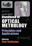
It is assumed that the light propagates in the z-direction. As the light propagates from medium n0 to ns, as shown in Figure 28.1, it is divided into two parts, reflection and transmission. The amplitude reflection coefficient and transmission coefficient, ρ and τ respectively, are expressed as [2]
where ψ is the phase change during reflection.
Figure 28.2 depicts a single layer with a refractive index n and a thickness d, coated on a substrate with a refractive index ns. This means the film has an optical thickness nd and a phase thickness δ = (2π/λ)nd, where λ is the wavelength of the incident light in a vacuum. There are two interfaces a and b. The incident medium can be air (n0 = 1), water (n0 = 1.33), or cement (n0 = 1.4–1.5). When the incident light reaches the first interface a, it is divided into reflected and transmitted parts with the amplitude reflection and transmission coefficients being ρa and τa, respectively. The transmitted light is reflected back to the incident medium when it reaches the second interface b. Its amplitude is denoted by ρb. Let ψa = φa and ψb be the phase changes as the light is reflected by interfaces a and b. Since ρb travels twice the thickness of the film, which introduces a phase delay −2δ, there is a phase change φb = −2δ + ψb in the reflected beam ρb.
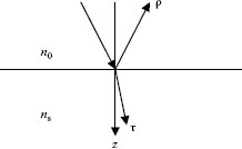
FIGURE 28.1 Light propagates from medium n0 to ns.
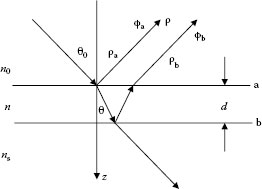
FIGURE 28.2 Single-layer film with a refractive index n and a thickness d coated on a substrate with a refractive index ns.
Thus ρa and ρb can now be expressed as follows [2,3]:
The resulting amplitude of the reflectance ρ is approximately the sum of the two beams ρa and ρb so that
The reflectance R represents the radiance of the detectable light [2,3]
Let the incident medium be air. In this case, n0 is always less than n. According to Equation 28.4, there is a phase shift ϕa = π for the reflected light ρa since −1 = exp(iπ). Depending on the magnitudes of the refractive indices of the film and the substrate, that is n > ns or n < ns, the two beams ρa and ρb will have constructive interference or destructive interference. The maximum interference happens at δ = (2m + 1)π/2 when the optical thickness of the film nd is an odd multiple of the quarter wave (2m + 1)λ/4, where m is an integer. Figure 28.3a and b depicts the two extreme cases: (1) the destructive maximum, where n < ns and ρa and ρb are out of phase π and (2) the constructive maximum, where n > ns and ρa and ρb are in phase.
When δ is not exactly a multiple of π/2, it means nd is not exactly a multiple of the quarter wave; the reflectance is still different from a bare substrate even though it is not as extreme. Figure 28.4 shows changes in the reflectance R as the film thickness increases. From Equation 28.7, we can derive the extreme of R which is at nd = (2m + 1)λ/4. Its value is
If we let the reflectance of a bare substrate be Rs, then Rs = [(1 – ns)/(1 + ns)][(1 – ns)/(1 + ns)]*. Therefore, it is clear that R < Rs when n < ns and R > Rs when n > ns. Please note that R = Rs at a multiple of the half-wave thickness nd = mλ/2. For this reason we call a layer with a half-wave thickness an absentee layer.
For the case shown in Figure 28.3a, if we set |ρa| = |ρb| or using Equation 28.8, we get R = 0 when , at the wavelength λ = 4nd. Let us denote this wavelength as the reference wave λ0. This is the so-called single-layer antireflection coating. For a BK-7 glass, ns = 1.52 and Rs = 4.26%, therefore, to have R = 0, n must be 1.23.
FIGURE 28.3 Two-beam interference from Figure 28.1: (a) destructive interference at λ = 4nd; and (b) constructive interference at λ = 4nd.
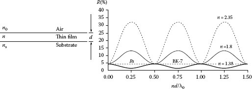
FIGURE 28.4 Changes of reflectance R as the film thickness increases.
On the other hand, for the case in Figure 28.3b, when the film has a refractive index n > ns, the larger the n, the higher the R. The maximum reflectance is again at the wavelength λ = 4nd, expressed by Equation 28.8. For ZnS, n = 2.35, deposited on BK-7, R = 32% and is a potential beam splitter.
For an oblique incident light at the angle θ, the optical thickness nd behaves as nd cos θ, so the phase thickness is changed to δ = (2π/λ) nd cos θ [2,3]. This explains why the colors of soap bubbles and oil films vary with the thickness of the layer and the incident angle.
The above derivation is approximate, but it is generally correct for a single-layer coating. It has the advantage of making it easy to see how a thin film affects a substrate optically. However, for multilayer analysis, it is more convenient and precise to use a matrix formulation where each layer is represented by a characteristic matrix M [2,3,4],
The matrix method has no approximation. When a layer with refractive index n and phase thickness δ = (2π/λ)nd is deposited on a substrate, the refractive index ns and interfaces “a” and “b” can be replaced by a single interface, as shown in Figure 28.5, with an equivalent refractive index nE expressed as follows:
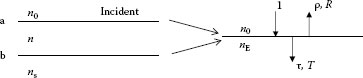
FIGURE 28.5 Two interfaces of a single-layer coating are replaced by a single interface with an equivalent refractive index nE.
We can now treat Figure 28.2 as in Figure 28.1 with the amplitude reflection and transmission coefficients ρ and τ expressed similar to Equations 28.2 and 28.3, that is,
The reflectance and transmittance become
It is easy to see that if the film thickness is an odd multiple of the quarter wave, that is, δ = (2m + 1)π/2, then, according to Equation 28.11, R is the maximum or minimum with the equivalent index nE = n2/ns. If the film thickness is a multiple of the half wave, that is, δ = mπ, M becomes a unity matrix. The reason has already been mentioned that a layer with an integral number of half-wave thicknesses is called as an absentee layer. This absentee layer is very useful in filter design, as we will see in the next section. For such special characterization in thin-film design we use the notations H and L to indicate a quarter-wave layer with the refractive indices higher and lower than the substrate, respectively, and the one with a refractive index in between is denoted as M, I, or J.
The matrix formulation can be extended to multilayer coatings, that is, m layers with the mth layer next to the substrate, as follows:
A multilayer coating with multi-interfaces is then replaced by a single interface with an equivalent refractive index nE = C/B, the same expression as in Equation 28.11; the reflectance and transmittance are expressed as in Equation 28.14.
28.3 SOME TYPICAL FILTERS AND THEIR DESIGN PRINCIPLES
Some typical filters and their design principles are described briefly in this section. Interested readers can refer to several sources for more details [2,3,4].
We have already looked at a single-layer antireflection coating (AR coating) in the last section. For BK-7, ns = 1.52, we need a film with a refractive index to make R = 0. However, there is no robust material where n = 1.23. The closest one is MgF2 (with n = 1.38) that, according to Equation 28.8, has a residual reflectance of R = 1.26%. To reduce R to zero, we should precoat a quarter-wave layer, named as M layer, with a material that has a refractive index of 1.7 such that ns is increased to the equivalent index nE = n2/ns = 1.9 and then , therefore R = 0. This describes a two-layer AR coating, customarily called a quarter-quarter coating, symbolized here by S/ML/A, where S and A stand for the substrate and the incident medium, in this case air. If we add a high refractive index half-wave layer 2H after the M layer, the R at the reference wavelength λ0 does not change, but the other wavelength is reduced. For this reason, a half-wave layer is called a broadening layer or a flattening layer. Figure 28.6 shows a comparison of several AR layering systems: S/M2HL/A (three-layer quarter-half-quarter), S/ML/A (two-layer, quarter-quarter), and S/L/A (single quarter-wave layer), where the high index material is assumed to be Ta2O5 with n = 2.15.
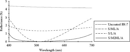
FIGURE 28.6 Single-layer, two-layer, and three-layer AR coatings.
Usually an operator likes to use only two high-quality materials with refractive indices that are as different as possible. Let us say, for example, that these two materials are Ta2O5 and SiO2 with refractive indices of 2.15 and 1.46, respectively. In this case, the M layer will be replaced by two non-quarter-wave layers, denoted as H′L′, with optical thicknesses of 0.084λ0 and 0.073λ0, respectively, where SiO2 is the last layer. The layering system thus becomes S/0.336H0.292L2HL/A.
28.3.2 HIGH REFLECTION COATING
A simple metallic film such as Ag, Al, Au, or Rh can also act as a high-reflection coating. However, to have low absorption it is necessary to have an all-dielectric multilayer. The basic design is to use a quarter-wave stack: S/H(LH)p/A. The equivalent refractive index from Equation 28.15 can now be expressed as in Equation 28.16. We thus find that the higher the p, the higher the reflectance
The width of the high-reflection zone 2Δg shown in Figure 28.7 can now be expressed as [2,3]
where g = λ0/λ is the relative wavelength. It can thus be seen that the higher the index ratio, the wider the 2Δg.
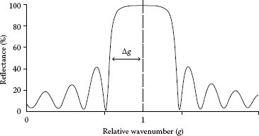
FIGURE 28.7 High-reflection coating composed of quarter-wave stacks with width 2Δg.
28.3.3 LONG-WAVE PASS AND SHORT-WAVE PASS FILTERS
A long-wave pass filter allows the transmission of long wavelengths but reflects short wavelengths; a short-wave pass filter allows the opposite. Color filter, cold mirror, heat mirror, UV-cut filter, and IR-cut filter are some examples. The basic design depends on symmetrical layers [4,5]. For example, S/(0.5HL0.5H)x/A and S/(0.5LH0.5L)x/A represent a long-wave pass filter and a short-wave pass wave filter, respectively. Usually we have to add some matching layers to increase the transmittance in the pass band; see Figure 28.8 [3]. The matching layer acts as an antireflection layer. The optical performance of long-wave pass filters and short-wave pass filters, with and without matching layers coated on germanium, where H and L indicate the Ge and ZnS quarter-wave layers, can be seen in Figures 28.9 and 28.10 [3]. One can use a computer simulation to increase the transmission in the pass-band by adjusting the thickness of some layers.
FIGURE 28.8 Symmetrical layers with an equivalent index E and matching layers nmS and nmA.
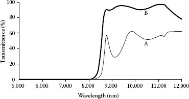
FIGURE 28.9 A: Ge/(0.5LH0.5L)7/A, λ0 = 6200 nm; B: Ge/1.47H(0.5LH0.5L)71.47L/A. (Adapted from Lee, C.C., Thin Film Optics and Coating Technology, 5th edn., Yi Hsien, Taipei, Taiwan, 2006.)
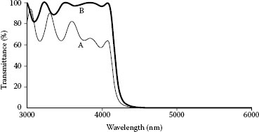
FIGURE 28.10 A: Ge/(0.5LH0.5L)7/A, λ0 = 5000 nm; B: Ge/0.79L(0.5LH0.5L)7/A. (Adapted from Lee, C.C., Thin Film Optics and Coating Technology, 5th edn., Yi Hsien, Taipei, Taiwan, 2006.)
The combination of a long-wave pass and a short-wave pass filter gives a fairly wide band-pass filter. To narrow the bandwidth (BW), we need a Fabry–Perot type filter (HR-Sp-HR) where HR is a high reflector that is made of an Al or Ag film or quarter stacks and Sp is a multiple half-wave layer called a spacer. Taking the quarter-wave stacks as HRs and an mth order spacer, we obtain a filter, S/H(LH)pm2L(LH)pHL/A, where the last layer L is an antireflection coating layer. The half peak BW Δλh of the filter is determined by p and m [2,3] and can be expressed as
This design is called the single-cavity filter and is approximately triangular in shape. To have a square top we need multiple cavities, as is the case, for example, of a three-cavity filter: | HR | Sp | HR | L | HR | Sp | HR | L | HR | Sp | HR |, where L is the coupling layer. Figure 28.11 depicts the spectra of the single-, two-, and three-cavity narrow band-pass filters.
28.3.5 BAND-STOP FILTER (RUGATE FILTER)
A band-stop filter, also called as a rugate filter, is opposite to the band-pass filter in that it reflects one or more specified bands. It can be realized by using an inhomogeneous film with index variation, as shown in Figure 28.12 [6,7,8]. The matching layers act as an antireflector to reduce ripples and suppress the sidelobes in the transmission regions. The half peak BW Δλh and the optical density of the stop band D can be expressed by Equations 28.20 and 28.21 where λc, na, np, and S are the center wavelength of the stop band, the average refractive index, the difference between the high and low indices, and the cycle of the inhomogeneous layer, respectively.
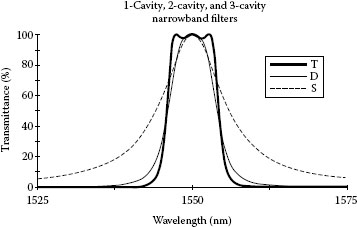
FIGURE 28.11 Spectra of the single- (S), two- (D), and three-cavity (T) narrowband-pass filters.
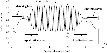
FIGURE 28.12 Index profile of a band-stop filter with matching layers for antireflection.
It is clear that the smaller the np, the narrower the Δλh, and the larger the S, the higher the reflection of the stop band. The spectrum of a typical rugate filter is shown in Figure 28.13.
A polarizer allows the passage of P-polarized light but reflects S-polarized light. For example, look at a tilted quarter-wave stack (S/(HL)pH/A) which acts as a plate polarizer for a small region of wavelengths, particularly in high-power lasers. To have a wide spectral region, the film stack has to be embedded between prisms (Prism/(HL)pH/Prism) designed at the Brewster angle so that there is no reflection of P-polarized light. A polarizer for light normally incident to the film can be fabricated utilizing sculptured film [9].
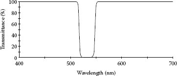
FIGURE 28.13 Spectrum of a rugate filter with matching and apodization layers center at 532 nm.
Various monitoring methods such as time counting, color recognition, quartz monitoring, and optical monitoring have been developed to control thickness during thin-film deposition. Optical monitoring is generally used in the manufacturing of optical thin-film filters [10,11]. Optical monitoring is based on changes of reflectance/transmittance as the film thickness increases; see Figure 28.4. The turning point method (TPM) is the most commonly used, and has the advantage of error compensation for quarter-wave stacks [11,12]. For nonquarterwave stacks, the wavelength of the monitoring system must be changed to an appropriate wavelength for monitoring each individual layer. Another method based on a single wavelength is called the level monitoring method [13]. This method is suitable for monitoring nonquarterwave multilayers. Error analysis shows that the monitoring plate must be precoated for error compensation. Several numerical methods and the optimum trigger point method have been developed to improve the performance, sensitivity, and compensation associated with the TPM and the level methods [14,15,16,17,18]. However, all of those monitoring methods use runsheet diagrams to control the thickness of the films based on their transmittance or reflectance. The refractive index n, the extinction coefficient k, and the thickness d are not independently determined in real time which makes phase extraction difficult. In a growing thin-film stack, the refractive index of the materials may change with time due to variations in the coating parameters or environmental fluctuations in the chamber, meaning we cannot terminate the current layer at the point specified in the original design. Therefore, real-time determination of n, k, and d is necessary for precision coatings. Ellipsometric and phase extraction methods have been proposed to solve this problem. Ellipsometric monitoring [19,20] requires algebraic computation to obtain the optical constants that fit the measurements, but require so many parameters that they are difficult to solve analytically. In the case of multilayer coatings, this could lead to the accumulation of errors, which would cause the final optical performance to differ from that of the original design.
To avoid this type of error accumulation, a new method, in situ sensitivity monitoring with proper error compensation, has been proposed to find the correct refractive index and physical thickness of each deposited layer [21]. An operator can choose the sensitivity monitoring wavelength that offers better error compensation for the reference wavelength. The result is better performance. Figure 28.14 shows the experimental results of the monitoring of a narrow band-pass filter with a center wavelength at 800 nm by this new method, the TPM, and the level method. The better performance of the new method is clear. The half peak BW and the position of the maximum transmittance are closer to the designed values than are those obtained using the other two methods. This is because TPM offers error compensation only for previous layers, but lacks sensitivity at termination points which results in a broadening of the BW. The level monitoring method has higher sensitivity, but no error compensation which results in a shift of the output spectrum. The new method on the other hand, combines the advantages of both methods, the sensitivity at termination points and the error compensation for previous layers.
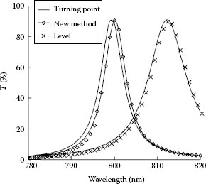
FIGURE 28.14 Spectra of narrow band-pass filters monitored by the three methods. (Adapted from Lee, C.C., and Wu, K., Opt. Lett., 32, 2118, 2007.)
Recently, a new polarization Fizeau interferometer-based monitoring system has been developed [22] which can get rid of the influence of the variations in the coating parameters caused by environmental fluctuations in the chamber. This is a vibration-insensitive in situ system, whereby one can instantly obtain the real-time phase and magnitude of the reflection coefficient and/or the transmission coefficient. The layout of a reflection monitoring system with a short coherence light source is shown in Figure 28.15. The test surface is located on one side of thin film growth, while on the other side of the substrate is the reference surface. The tunable retarder is composed of two wedge x-cut uniaxial birefringent crystals. The crystal-induced phase difference between two orthogonally polarized beams has to match the difference in the optical phase induced by the reference surface and the test surface. The interference will therefore occur only between either the S-polarized reference beam and the P-polarized test beam or the P-polarized reference beam and the S-polarized test beam. Other reflections from the interfaces will be suppressed because of the short coherence length of the light source [23]. Interference will occur when the transmission axes of the polarizers are oriented 45° and −45° to the fast axis of the birefringent crystal. These two polarizers as well as the other two (whose transmission axes are oriented 0° and 90°to the fast axis of the birefringent crystal) are combined and detected by the compact polarizer detector array, as shown in Figure 28.16. The magnitude of the reflection coefficient and the phase can be acquired from the phase-shifted interferograms of two orthogonal polarization beams on the detector array (after mathematical analysis using Equations 28.22 and 28.23). We now have complete information about the growing film stack and are able to accurately monitor the thickness of the whole stack.
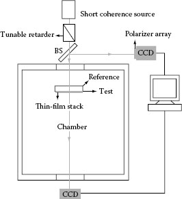
FIGURE 28.15 Schematic representation of the reflection optical monitoring system. (Adapted from Lee, C.C. et al., Opt. Express, 15, 17536, 2007.)
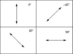
FIGURE 28.16 Layout of the polarizer detector array.
where
Ij is the reflectance of j = 0°, −45°, +45°, and 90° on the detector array
ρr and ρst are the reflection coefficients from the substrate to air and the deposited film stack, respectively
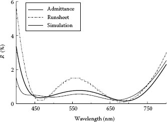
FIGURE 28.17 Optical performance of an antireflection coating obtained by admittance diagram and the conventional runsheet method. (Adapted from Chen, Y.R. and Lee, C.C., Monitoring of multilayer by admittance diagram, Conference on Optical Interference Coatings, Technical Digest, PWC7, Optical Society of America, Washington, DC, 2007.)
ϕ0 is the phase shift caused by the optical path difference between two orthogonal polarizations as they pass through the substrate and the retarder. ϕ0 can be acquired before the deposition of the thin film. Therefore, the phase of the thin-film stack’s reflection coefficient can be obtained. We now have complete information about the whole stack and each layer can be deposited with the correct thickness.
Better-monitoring performance can be achieved from an admittance diagram than a runsheet diagram because of the higher sensitivity and larger amount of physical and visual information. It has therefore been proposed that they be used in a new optical monitoring method [24,25,26]. The diagram is obtained by plotting the locus of the effective admittance during the deposition process. Changes in the refractive index during the coating process can be easily observed and immediately compensated for from layer to layer. Figure 28.17 shows plots of the optical performance of an antireflection coating monitored using a real-time admittance diagram and the conventional runsheet method.
28.5 CHARACTERIZATION OF A COATED FILM FROM OPTICAL MEASUREMENTS
Characterizing the optical properties of a coated film is very important for improving the quality and the functionality of the film and the resultant filter. There are several methods that have been used to do this and they can be classified into two categories: ellipsometric and photometric. Ellipsometry is based on the measurement of the complex amplitude reflections in the P and S directions, rp and rs, respectively. We obtain the ratio ρ and the phase difference Δ for rp and rs,
ψ and Δ are called the ellipsometric angles and are used for calculating the refractive index n, the extinction coefficient k, and the thickness d of the coated film through a numerical fitting algorithm [27,28,29].
Photometry is based on the measurement of the reflectance R(λ) and the transmittance T(λ). The R(λ) and T(λ) of a coated film can be obtained from spectrophotometric measurements. The techniques for measuring R(λ) and T(λ) have been described in several articles, interested readers can refer to Ref. [30] for more details. The refractive index n(λ), the extinction coefficient k(λ), and the thickness d of a coated film can be determined from R(λ) and T(λ). For example, look at the envelope method first proposed by Manifacier et al. [31] and then by Swanepoel [32]. First, the refractive index of the substrate ns is calculated using Equation 28.27; n, k, and d can now be derived from TM and Tm using Equations 28.28 through 28.30, as shown in Figure 28.18, where TM and Tm represent the maximum and minimum of the spectrum fringe, respectively. Each TM and Tm pair shall be at the same wavelength during the calculation.
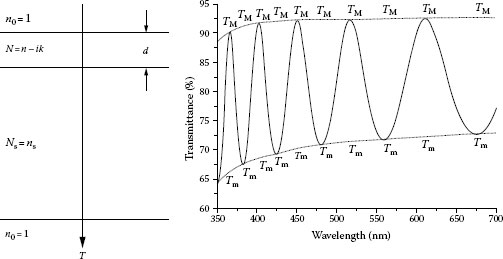
FIGURE 28.18 Envelope method for calculating the n, k, and d of a coated film.
Note that the n(λ), k(λ), and d obtained from above equations still need to be refined to fit an optimum solution, especially for an inhomogeneous film [33,34].
There are several other methods for measuring n(λ), k(λ), and d developed based on optical metrology, for example, the wave guide technique [35] and attenuated total reflection [36], which are also valuable references for those interested in thin film research. Accurate measurements of the optical constants of thin films by these techniques are indispensable for thin-film-related applications.
Δ |
phase thickness |
θ |
angle of incidence in a medium |
λ |
wavelength |
λ0 |
reference wavelength |
λc |
center wavelength |
Δλh |
half peak bandwidth |
ρ |
reflection coefficient; ratio of rp and rs |
τ |
transmission coefficient |
φ, ϕ |
phase shift |
ω |
angular frequency |
Δ |
ellipsometry angle |
ψ |
ellipsometry angle; phase change |
d |
film thickness |
n |
refractive index |
k |
extinction coefficient |
nE |
equivalent refractive index |
g |
relative wavelength |
rp |
complex amplitude reflection in the P direction |
rs |
complex amplitude reflection in the S direction |
Δ |
phase difference of rp and rs |
BW |
half peak bandwidth |
D |
optical density |
E |
amplitude of electric field |
H |
quarter-wave layer of high index |
HR |
high reflector |
I |
intensity |
L |
quarter-wave layer of low index |
M |
characteristic matrix; quarter-wave layer of intermediate index |
R |
reflectance |
S |
substrate |
Sp |
spacer |
T |
transmittance |
TPM |
turning point method |
1. M. Born and E. Wolf, Principles of Optics, 7th edn., Cambridge University Press, New York, 1999.
2. H. A. Macleod, Thin-Film Optical Filters, 3rd edn., Institute of Physics Publishing, Bristol, U.K., 2001.
3. C. C. Lee, Thin Film Optics and Coating Technology, 5th edn., Yi Hsien, Taipei, Taiwan, 2006.
4. A. Thelen, Design of Optical Interference Coatings, McGraw-Hill Book Company, New York, 1989.
5. L. I. Epstein, The design of optical filter, J. Opt. Soc. Am. 42, 806–810, 1952.
6. W. H. Southwell, Spectral response calculations of rugate filters using coupled-wave theory, J. Opt. Soc. Am. A5, 1558–1564, 1988.
7. W. H. Southwell and R. L. Hall, Rugate filter sidelobe suppression using quintic and rugated quintic matching layers, Appl. Opt. 28, 2949–2951, 1989.
8. W. H. Southwell, Using apodization functions to reduce sidelobes in rugate filters, Appl. Opt. 28, 5091–5094, 1989.
9. I. J. Hodgkinson and Q. H. Wu, Birefringent Thin Films and Polarizing Element, World Scientific, Singapore, 1997.
10. B. Vidal, A. Fornier, and E. Pelletier, Wideband optical monitoring of nonquarter wave multilayer filter, Appl. Opt. 18, 3851–3856, 1979.
11. H. A. Macleod, Monitor of optical coatings, Appl. Opt. 20, 82–89, 1981.
12. H. A. Macleod, Turning value monitoring of narrow-band all-dielectric thin-film optical filters, Opt. Acta 19, 1–28, 1972.
13. F. Zhao, Monitoring of periodic multilayer by the level method, Appl. Opt. 24, 3339–3343, 1985.
14. C. J. van der Laan, Optical monitoring of nonquarterwave stacks, Appl. Opt. 25, 753–760, 1986.
15. B. Bobbs and J. E. Rudisill, Optical monitoring of nonquarterwave film thickness using a turning point method, Appl. Opt. 26, 3136–3139, 1987.
16. C. Zang, Y. Wang, and W. Lu, A single-wavelength monitoring method for optical thin-film coatings, Opt. Eng. 43, 1439–1443, 2004.
17. C. C. Lee, K. Wu, C. C. Kuo, and S. H. Chen, Improvement of the optical coating process by cutting layers with sensitive monitor wavelength, Opt. Express 13, 4854–4861, 2004.
18. A. V. Tikhonravov and M. K. Trubetskov, Eliminating of cumulative effect of thickness errors in monochromatic monitoring of optical coating production: Theory, Appl. Opt. 46, 2084–2090, 2007.
19. J. Lee and R. W. Collins, Real-time characterization of film growth on transparent substrates by rotating-compensator multichannel ellipsometry, Appl. Opt. 37, 4230–4238, 1998.
20. S. Dligatch, R. Netterfield, and B. Martin, Application of in-situ ellipsometry to the fabrication of multilayered coatings with sub-nanometre accuracy, Thin Solid Films 455–456, 376–379, 2004.
21. C. C. Lee and K. Wu, In situ sensitive optical monitoring with error compensation, Opt. Lett. 32, 2118–2120, 2007.
22. C. C. Lee, K. Wu, S. H. Chen, and S. J. Ma, Optical monitoring and real time admittance loci calculation through polarization interferometer, Opt. Express 15, 17536–17541, 2007.
23. B. Kimbrough, J. Millerd, J. Wyant, and J. Hayes, Low coherence vibration insensitive Fizeau interferometer, Proc. SPIE 6292, 62920F, 2006.
24. Y. R. Chen, Monitoring of film growth by admittance diagram, Master thesis, National Central University, Jhongli, Taiwan, 2004.
25. B. J. Chun, C. K. Hwangbo, and J. S. Kim, Optical monitoring of nonquarterwave layers of dielectric multilayer filters using optical admittance, Opt. Express 14, 2473–2480, 2006.
26. Y. R. Chen and C. C. Lee, Monitoring of multilayer by admittance diagram, Conference on Optical Interference Coatings, Technical Digest, Optical Society of America, PWC7, Washington, DC, 2007.
27. R. M. A. Azzam and N. M. Bashara, Ellipsometry and Polarized Light, North-Holland Publishing Company, Oxford, U.K., 1977.
28. C. W. Chu, The research on the calculation of optical constant of optical thin film, PhD thesis, Institute of Optical Sciences, National Central University, Jhongli, Taiwan, 1994.
29. J. Rivory, Ellipsometric measurements, in Thin Films for Optical System, Chapter 11, edited by Flory, F. R., Marcel Dekker, Inc., New York, 1995.
30. J. P. Borgogno, Spectrophotometric methods for refractive index determination, in Thin Films for Optical System, Chapter 10, edited by Flory, F. R., Marcel Dekker, Inc., New York, 1995.
31. J. C. Manifacier, J. Gasiot, and J. P. Filland, Simple method for determination of the optical constant n, k and the thickness of weekly absorbing thin films, J. Phys. E: Sci. Instrum. 9, 1002–1004, 1976.
32. R. Swanepoel, Determination of the thickness and optical constant of amorphous silicon, J. Phys. E: Sci. Instrum. 16, 1214–1222, 1983.
33. J. P. Borgogno, F. Flory, P. Roche, B. Schmitt, G. Albert, E. Pelletier, and H. A. Macleod, Refractive index and inhomogeneity of thin films, Appl. Opt. 23, 3567–3570, 1984.
34. Y. Y. Liou, C. C. Lee, C. C. Jaing, and C. W. Chu, Determination of the optical constant profile of thin weekly absorbing inhomogeneous films, Jpn. J. Appl. Phys. 34, 1952–1957, 1995.
35. F. R. Flory, Guided wave techniques for the characterization of optical coatings, in Thin Films for Optical System, Chapter 15, edited by Flory, F. R., Marcel Dekker, Inc., New York, 1995.
36. T. Lopez-Rios and G. Vuye, Use of surface plasmon excitation for determination of the thickness and optical constants of very thin surface layers, Surf. Sci. 81, 529–538, 1979.