
CONTENTS
29.2 Profiling of a Thick Transparent Film by White-Light Interferometry
29.2.1 White-Light Interferometry
29.2.2.2 Calculation Procedure
2.3 Film Profiler with the KF Algorithm
29.2.4 Range of Measurable Film Thickness
29.2.5 Examples of Measurements
29.2.5.1 Steps in Film Thickness
29.2.5.2 Resist Film with an Unknown Refractive Index
29.2.5.3 Repeatability of Measurement
29.3 Profiling of a Thin Transparent Film
29.3.1 Measurement of an Oxide Thin Film Step
29.3.2 Measurement of CMP Samples
29.4 Film Thickness Profiling by Pseudo-Transmission Interferometry
29.4.1 Principle of the TF Method
29.5 Simultaneous Measurement of Thickness and Refractive Index
29.6 Film Thickness Profiling by Three Wavelength Interference Color Analysis
29.6.1 Introduction to the Interference Color Analysis Technique
29.6.2 Principle of the GMFT Method
29.6.4 Examples of Measurements
The technique of surface profile measurement using optical interference is widely used in industry as a noncontact and nondestructive method of quickly and accurately measuring the profile of microscopic surfaces. However, its application to transparent thin films has been limited because it is difficult to obtain an exact surface profile measurement if the surface to be measured is covered with a transparent film. This is because the interference beam coming from the back surface of the film creates disturbance.
Thickness profile measurement is also of great importance in industry; for example, the measurement of various kinds of thin film layers on substrates of semiconductors or flat panel display devices. There are several different techniques used to measure these films, of which the most widely used are reflection spectrophotometry and ellipsometry.
In the case of freestanding films such as plastic films, there are also several nondestructive measurement techniques, such as methods using β-rays, infrared (IR) or nuclear gauges, and spectrophotometry.
However, most of these techniques are limited to single-point measurement. To obtain an aerial thickness profile, it is necessary to mechanically scan the sample or the sensing device. Another limitation inherent in these techniques is their large spot sizes. For example, spectrophotometers are limited to spot sizes of a few micrometers or greater because of available light budgets.
Many techniques have been proposed to resolve these problems in the surface and thickness measurement of substrate-supported films and freestanding films. This chapter introduces some of the techniques to realize surface and thickness profile measurement of a transparent film by means of optical interferometry or interference color analysis.
29.2 PROFILING OF A THICK TRANSPARENT FILM BY WHITE-LIGHT INTERFEROMETRY
29.2.1 WHITE-LIGHT INTERFEROMETRY
Figure 29.1 shows the optical section of a microscopic surface profiler using white-light interferometry.
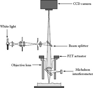
FIGURE 29.1 Schematic illustration of an interference microscope.
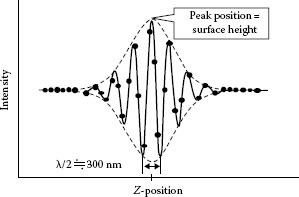
FIGURE 29.2 An example of a white-light interferogram. The black dots indicate sampled values, and the dotted line denotes the envelope.
The equipment uses white light as the light source, and when it performs a vertical scan along the Z-axis of the interference microscope, the intensity signal of one charge-coupled device (CCD) pixel changes, as shown in Figure 29.2, maximizing the modulation of the interference fringe at the point where the difference in the path length between the measurement light path and the reference light path becomes zero. By determining the Z-axis height that corresponds to the largest interference fringe modulation at every point in the TV camera, this technique measures en bloc the threedimensional profile in the field of view (FOV) of the camera.
Various algorithms have been proposed to detect the peak position of modulation [1,2,3,4,5], most of which assume that the peak is single. Therefore, if a film-covered surface is measured, superposition occurs between the reflected beams from the front surface and the reflected beams from the back surface, hampering correct measurement of the surface profile.
It has long been known that if the thickness of a transparent film is greater than the coherent length, two peaks of reflection corresponding to the front and back surfaces appear on the interferogram, allowing simultaneous measurement of film thickness and surface height variations from those peak positions [6,7,8,9,10].
However, the methods reported to date either require visual determination of the peak positions [1,2,3,4,5,6,7] or use a complex calculation algorithm [9,10], and no automatic measuring device was available on the market for practical use until our development of such a device in 2002 [11].
We developed an algorithm, the thicK Film (KF) algorithm [12], that is able to automatically detect the positions of two contrast peaks in an interferogram generated by white-light vertical scanning interferometry (VSI). This algorithm calculates the interference amplitudes from an interferogram. The results are interpreted as a histogram, and the automatic threshold selection method [13] then finds the optimal threshold for peak separation. Finally, the peak position is determined for each of the distinct peak regions. We will explain this algorithm using a calculation example in the sections that follow.
An oxide film with a thickness of approximately 1 μm formed on an Si wafer was measured. A halogen lamp was used as the light source, and the Z-axis scanning speed was set at 2.4 μm/s with a sampling interval of 0.08 μm. Figure 29.3 shows the obtained interferogram.
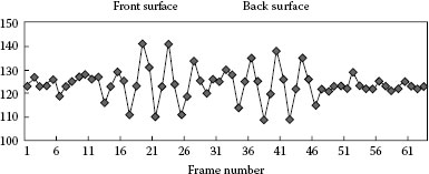
FIGURE 29.3 Interferogram used for the KF algorithm test. An oxide film with a thickness of approximately 1 μm on an Si wafer was measured. The sampling interval was 80 nm.
29.2.2.2 Calculation Procedure
1. Step 1: Calculation of contrast
First, determine the average value of the intensity data and then calculate the AC components by subtracting the average value from each piece of data. By squaring the AC components for the purpose of rectification, we obtain the contrast data of interference shown in Figure 29.4.
2. Step 2: Separation of peaks
Taking the contrast data shown in Figure 29.4 as a histogram, determine the optimal threshold for peak separation using Otsu’s automatic threshold selection method in the field of processing to binary value imagery [13].
More specifically, given a set of frequency values n(i), (i = 1, L), where the number of observed value levels is L, and the observed value level is i, we take the intraclass variance, expressed by the following equation, as an objective function and choose the threshold that minimizes the function:
where
ω1 and ω2 are the frequencies of the classes
and are the variances of the classes
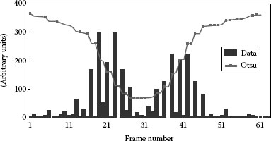
FIGURE 29.4 Contrast data and Otsu’s objective function for automatic threshold selection.
The values of the objective function are shown by the solid-line curve in Figure 29.4, with frame number 30 being the threshold.
3. Step 3: Detection of peak position
Frame number 30 separates the distribution into left and right peak regions. For each region, the peak positions were detected by conventional methods.
4. Step 4: Calculation of two surface heights and one film thickness
Let the heights converted from the peak positions be zp1 and zp2, and let the refractive index of the film be n. Then,
a. The surface height of the transparent film = zp1
b. The film thickness t = (zp1 – zp2)/n
c. The back-surface height of the film = zp1 – t
29.2.3 FILM PROFILER WITH THE KF ALGORITHM
Using the KF algorithm, Toray Engineering Co. developed the noncontact Film Profiler SP-500F shown in Figure 29.5, which allows simultaneous measurement of the front and back surface topography and the thickness variation of a transparent film.
This development allows the following measurements, which are difficult to perform under conventional methods:
1. Profiling of a surface covered with a transparent film
2. Profiling of a bottom surface through a transparent film
3. 2-D measurement of film thickness distribution
This system has already been introduced and used effectively in the semiconductor, LCD, and film manufacturing processes [11].
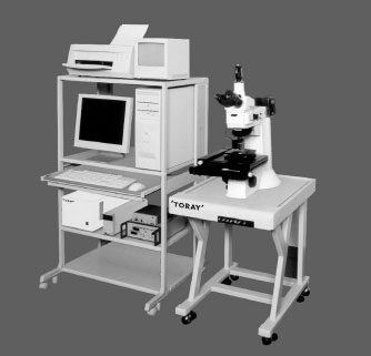
FIGURE 29.5 SP-500F film profiler.
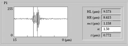
FIGURE 29.6 Interferogram of an oxide film on an Si wafer. The measured thickness was 0.77 μm.
29.2.4 RANGE OF MEASURABLE FILM THICKNESS
The KF method of measurement has a lower limit of measurable film thickness because it is based on the assumption that interferogram peaks can be separated. Oxide films with a thickness of 0.5–2 μm on an Si wafer were measured, and the minimum measurable thickness was found to be approximately 0.8 μm. Figure 29.6 shows the interferogram of a 0.77 μm oxide film, which is the lowest measurable range to date.
29.2.5 EXAMPLES OF MEASUREMENTS
29.2.5.1 Steps in Film Thickness
A step in an oxide film formed on an Si wafer was measured, and the results are shown in 3-D representation in Figure 29.7. The measured surface step was 2.9 μm, and the film thickness was 4.0 μm in the higher area and 1.1 μm in the lower area. These thickness values agreed fully with the measurements obtained by ellipsometry. It was also found that the back surface was correctly measured as a flat surface with a supposed refractive index of 1.46.
29.2.5.2 Resist Film with an Unknown Refractive Index
The thickness distribution of a resist film on a glass plate was measured. Since the refractive index of the resist film was unknown, part of the film was peeled off, and the film profile was then measured. The surface step, which is equal to the physical thickness (t), was approximately 1.6 μm at the peeled portion, and the optical thickness (n·t) was about 3.0 μm. These measurements allowed us to estimate the refractive index (n) at approximately 1.9.
The accuracy of the refractive index can be justified by the fact that the plate surface of the peeled portion and the back surface of the film are flush on the same plane. The back surface profiles calculated with three different refractive indexes are shown in Figure 29.8. A visual estimation gives a result of n = 1.90 ± 0.02.
The film thickness and back surface height were then recalculated with the obtained refractive index; the results are shown in Figure 29.9.
29.2.5.3 Repeatability of Measurement
An oxide film on an Si wafer was measured repeatedly, giving the results shown in Figure 29.10. The measurement of film thickness produced the following data: mean value = 4.609 μm; standard deviation (σ) = 17 nm; and CV value = 0.36%.
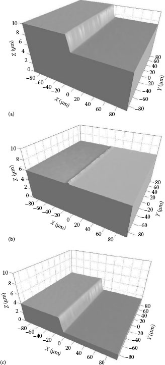
FIGURE 29.7 Measurement results of an SiO2 film step on an Si wafer. (a) Front surface, (b) back surface, and (c) thickness.
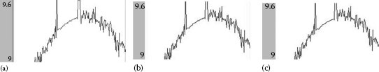
FIGURE 29.8 Back surface profiles calculated with different refractive indexes (n). The peeled area is located at center left. (a) n = 1.88, (b) n = 1.90, and (c) n = 1.92.
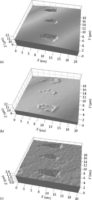
FIGURE 29.9 Measurements of a resist film. (a) Front surface, (b) back surface, and (c) thickness.
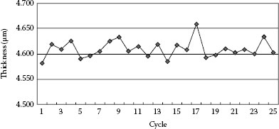
FIGURE 29.10 Repeatability of film thickness measurement.
29.3 PROFILING OF A THIN TRANSPARENT FILM
When a film becomes very thin, the KF algorithm can no longer be applied due to the overlap of two interference peaks. To solve this problem, several methods have been proposed [14,15,16], but as yet, there is no appropriate commercial product on the market. We developed an algorithm, the thiN Film (NF) algorithm, which can measure the 3-D surface profiles of a surface covered by a thin film and is robust enough for practical use in industry. Using this algorithm, Toray Engineering Co. developed the noncontact Surface Profiler SP-700 for thin film–covered surfaces. Oxide films with a thickness of 0–2000 nm on an Si wafer were measured, and the minimum measurable thickness was found to be 10–50 nm.
29.3.1 MEASUREMENT OF AN OXIDE THIN FILM STEP
An oxide thin film step with thicknesses of 100 and 300 nm was prepared on an Si wafer. Its cross section is shown in Figure 29.11. The test results given in Figure 29.12 show good agreement between the obtained and predicted values.
The repeatability of the film thickness measurement is shown in Figure 29.13. The thickness was an average of 10 × 10 pixels. The average and sigma of 25 repeated measurements were 301.5 ± 0.21 nm for the thicker film and 99.3 ± 0.30 nm for the thinner film.
29.3.2 MEASUREMENT OF CMP SAMPLES
Figure 29.14 shows the measurement results of oxide chemical mechanical polishing (CMP) samples with three different polish times (0, 20, and 60 s). The front surface profiles show rapid change due to the polish. The back surface profiles, on the other hand, show no change because polishing occurs only within the oxide film layer. Figure 29.15 shows the detailed top surface profile of the 60 s sample. The film thicknesses underneath are 466 nm at the center area and 740 nm in the surrounding area. From this simultaneous measurement of surface topography and film thickness distribution, we can obtain fast, vital, and unique information on the CMP process.
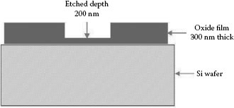
FIGURE 29.11 Cross section of the thin film sample.
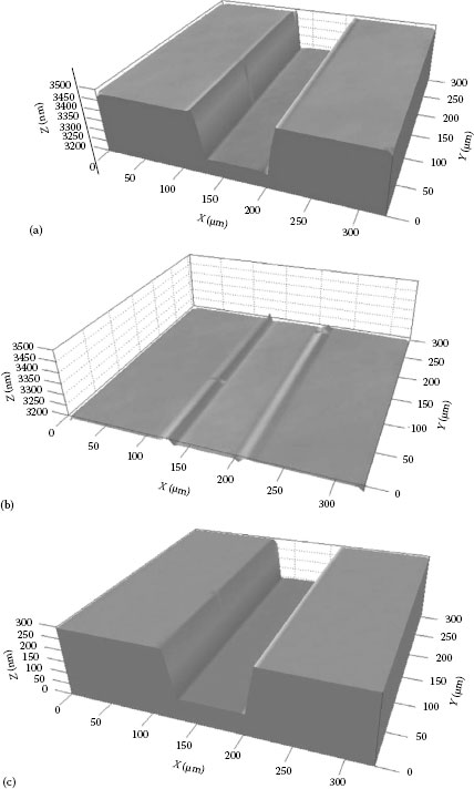
FIGURE 29.12 Thin film measurement results. (a) Front surface, (b) back surface, and (c) thickness.
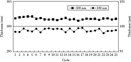
FIGURE 29.13 Repeatability of thin film thickness measurement.
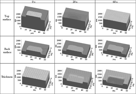
FIGURE 29.14 Measurement results of three CMP samples.
29.4 FILM THICKNESS PROFILING BY PSEUDO-TRANSMISSION INTERFEROMETRY
29.4.1 PRINCIPLE OF THE TF METHOD
When we measure a freestanding film like a plastic film, there is another approach. This method, the transmission film (TF) method [17], measures a reasonably flat mirror surface with a sample film placed on it halfway into the FOV. The surface through the film is then measured at a point lower than the surface without the film by (n – 1)t, as shown in Figure 29.16, because of the optical path difference (OPD) (D) between air and the film. If the refractive index (n) is known, the thickness (t) is calculated from the OPD.
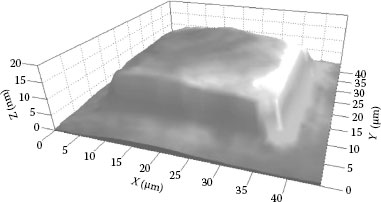
FIGURE 29.15 Detailed top surface profile of the 60 s CMP sample measured by the SP-700. The height of the pattern is on the order of 10 nm, and the film thickness underneath is 460–740 nm.
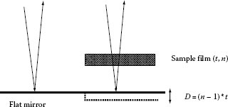
FIGURE 29.16 Principle of the TF method.
If the working distance is not long enough to insert the sample halfway in the FOV, we can obtain the OPD by two successive measurements, the first obtained without the film and the second obtained with the sample.
Since any conventional technique for measuring a flat surface, such as phase-shift interferometry, can be used in this technique, measurement of sub-nanometer thickness is theoretically possible. Another advantage of this technique is its robustness. Since the optical path length does not depend on the film position, its vibration or bending does not affect the measurement.
Polyester (PET) films with thicknesses of 0.9–6.0 μm were measured using this technique. As the reference mirror, we used a metal substrate for hard disk drive. The surface was measured by white-light VSI with a scanning speed of 2.4 μm/s. The sample was inserted only in the right half of the FOV. Figure 29.17 shows the measured mirror surface profile, the right half through a PET film with a nominal 0.9 μm thickness.
The average height difference between the left and right areas was 0.58 μm. From this value and the nominal refractive index of 1.65, we obtained the film thickness of 0.89 μm.
Figure 29.18 shows the correlation between the measured thicknesses and the nominal values. The obtained film thickness values agree well with the nominal values.
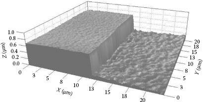
FIGURE 29.17 Measured surface profile of a mirror surface, with a PET film of a nominal 0.9 μm thickness inserted in the right half.
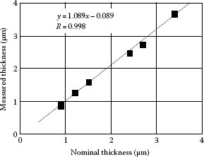
FIGURE 29.18 Correlation between the measured values and the nominal values.
29.5 SIMULTANEOUS MEASUREMENT OF THICKNESS AND REFRACTIVE INDEX
A freestanding polyester film nominally 1.5 μm in thickness was measured using the KF and TF methods. Figures 29.19 and 29.20 show the thickness profiles obtained by the KF and TF methods, respectively. These data were obtained using the nominal refractive index value of 1.65. The upper-right corner is marker ink. The results are largely consistent with each other with the exception of the error along the film edge in the TF method, which is due to the defocus effect of the microscope.
Figure 29.21 shows a comparison of two thickness profiles along a certain horizontal line. Note that there is a bias between them, probably due to an error in the nominal refractive index. From this, we observe that it is possible to obtain the thickness and the refractive index simultaneously by combining the results of two measurements: the optical thickness T by the KF method, and the OPD D by the TF method [18].
Since T = nt and D = (n – 1)t, the thickness (t) and the refractive index (n) can be obtained by the following equations:
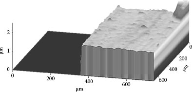
FIGURE 29.19 Film thickness profile by the KF method.
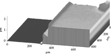
FIGURE 29.20 Film thickness profile by the TF method.
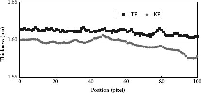
FIGURE 29.21 Film thickness profiles obtained by the TF and KF methods with a nominal refractive index.
and
Figure 29.22 shows the obtained thickness and refractive index profiles along a horizontal line. This technique was mentioned briefly in the description of an old patent [19] but seems to have remained almost unknown until now. Compared with other proposed techniques [20,21], this technique is simple and easily accomplished by a commercial surface profiler.
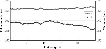
FIGURE 29.22 Film thickness and refractive index profiles calculated from the results of the KF and TF methods.
29.6 FILM THICKNESS PROFILING BY THREE WAVELENGTH INTERFERENCE COLOR ANALYSIS
29.6.1 INTRODUCTION TO THE INTERFERENCE COLOR ANALYSIS TECHNIQUE
The interference color phenomenon of thin films is seen in soap bubbles, and the relation between the color and the thickness of a film has been investigated for many years and is represented in the Newton color chart. The knowledge of this relation has been used for measuring semiconductor film thickness [22,23], the flying height of magnetic heads [24], and lubricant film thickness [25,26]. A typical example is the lubricant film thickness measurement system described by Eguchi and Yamamoto [26], in which a color camera captures the interference image, and the film thickness at each pixel is estimated from its hue by using the calibration data obtained in advance.
However, techniques based on the use of the interference color have rarely been used in the industry. The most serious problem with these techniques is that they require frequent calibration because the color thickness relation depends on a variety of environmental conditions such as the illumination and the target film structure. Another problem is their narrow unambiguous measurement range of a few hundred nanometers, resulting from the cyclic repetition of colors depending on the thickness.
To overcome these problems, we have developed a novel 2-D film thickness measurement method, named global model fitting for thickness (GMFT) [27], which is an extension of the global model fitting algorithm developed for three-wavelength interferometric surface profiling [28]. We validated the GMFT method by using both simulations and experiments.
29.6.2 PRINCIPLE OF THE GMFT METHOD
The algorithm consists of two steps, and its flowchart is shown in Figure 29.23.
Step 1 consists of the GMFT method, which is used to estimate the thickness of each pixel from its color information. Because of the high computational cost, this method is applied to a limited number of pixels during actual use. Step 2 consists of another method, named ACOS, which calculates the thickness of the other pixels within a shorter period of time by using the information obtained from step 1. This information is also applicable to other images captured under the same optical conditions. For this reason, it can be referred to as a “recipe.”
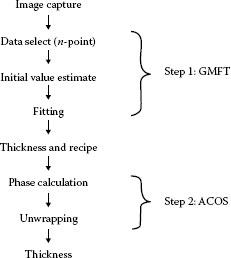
FIGURE 29.23 Flowchart of the GMFT algorithm.
29.6.2.1.1 Relationship between Color and Thickness
Consider light incident on a thin film and reflected by both the upper and lower boundaries. After ignoring multiple reflections, we can obtain the following intensity of the sum of the two reflected waves:
where
I1 and I2 are the intensities of the waves
λ is the wavelength
δ is the phase difference between them
Assuming a uniform refractive index, n(λ), and normal incidence of light, the OPD between the two reflections from a thin film is OPD = 2n(λ)t, where t is the thickness of the layer. Therefore, the phase difference for light reflected from the two surfaces is δ(λ) = 2π OPD/λ = 4πn(λ)t/λ. For a nondispersive medium (i.e., n(λ) = n), we obtain
Let us consider a case of three-wavelength (B, G, and R) illumination. By assuming that I1 = I2 = 1/2, λB = 470 nm, λG = 560 nm, and λR = 600 nm, we calculated the theoretical intensities of each wavelength for the optical thickness range 0–1000 nm and then obtained the synthesized color chart. The results are shown in Figure 29.24.
It should be noted that the color change is due to the cyclic variation in BGR signals according to the film thickness. This means that we can estimate the film thickness from the BGR signals instead of from the color information.
Three-wavelength BGR signals can be obtained by an interference color imaging system, which is shown in Figure 29.25.
This is almost the same configuration as that of the three-wavelength single-shot interferometry reported by Kitagawa [29]. The details of the actual apparatus used in the experiment are described in Section 29.6.3.
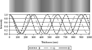
FIGURE 29.24 BGR intensities and synthesized color chart as a function of film thickness.
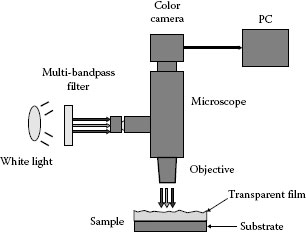
FIGURE 29.25 Microscopic optical setup for three-wavelength interference color imaging.
29.6.2.1.2 GMFT ALGORITHM
Although the case of three wavelengths was considered in Figure 29.24, in the following equations, we assume a more generalized expression for m wavelengths.
When we capture interference images of m wavelengths, the observed intensity g(i, j) at the point i (i = 1, 2, …, n) and for wavelength j (j = 1, 2, …, m) is given by the following model:
where a(j) and b(j) are the DC bias and the modulation of the waveform, respectively, and φ(i, j) is the phase given by
where
n is the known refractive index
t(i) is the thickness
λj is the wavelength of the jth wavelength
Inserting Equation 29.7 into Equation 29.6 gives the following model:
This model is derived under the assumption that the waveform parameters a(j) and b(j) are constant in the FOV and dependent only on the wavelength. This assumption is almost always valid when the target surface is homogeneous.
The unknown parameters a(j), b(j), and t(i) can be estimated using the following least-squares fitting equation:
where
g(i, j) is the model intensity defined by Equation 29.8
gij is the observed intensity
This nonlinear least-squares problem can be solved by many numerical methods. In our experiments, we used the Davidon–Fletcher–Powell algorithm [30].
29.6.2.1.3 Necessary Conditions
Let us consider the necessary conditions to obtain the unknown parameters a(j), b(j), and t(i). When the number of wavelengths is m and the number of points is n, the total number of unknown parameters is 2m + n. Since m values are observed at one point, the necessary condition for the solution is mn ≥ 2m + n. Then, the number of points must be
This means that n ≥ 4 in the case of m = 2, and n ≥ 3 in the case of m = 3. When n = 2m/(m – 1), then the problem becomes a (2m + n)-order nonlinear simultaneous equation, and when n > 2m/(m – 1), then the problem becomes a (2m + n)-order nonlinear least-squares problem.
Figure 29.26 illustrates the principle of this algorithm in the case of three wavelengths and n-points. From 3n observed intensities, we can estimate (n + 6) unknown parameters, that is, n-point thicknesses and six waveform parameters.
It should be noted that to avoid the problem from becoming ill-conditioned and to obtain a good estimation, it is advisable to select the points such that their thickness distribution becomes wide.
29.6.2.1.4 Initial Estimates
To find solutions to the nonlinear least-squares problem described in the previous section, we use an iterative technique, which requires initial estimates that allow us to search for the minimum. Since the model function of Equation 29.8 contains a cosine function, the error function has many local minima. Therefore, it is essential to make good initial estimates.
In our experiments, a(j) is set to be the average of the observed values, and the modulation b(j) is set to be the range of the observed values (i.e., the difference between the maximum and minimum observed values) divided by 2a(j). The thickness, t(i), is a rough estimate, which is generally given by a priori knowledge of the target sample.
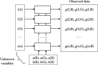
FIGURE 29.26 Principle of the GMFT method in the case of three wavelengths and n-point fitting.
The computational cost of the nonlinear least-squares problem is very high. Hence, the method becomes impractical when the number of points is large. Therefore, we use the GMFT algorithm with a small number of points (e.g., under 100), and then the thicknesses of the other points are calculated by the following method, named the ACOS method, which uses the estimated waveform parameters from the first step.
29.6.2.2.1 Phase Estimation
When the waveform parameters are given, the phase is obtained from the observed intensity by the following equation derived from Equation 29.6:
where cos−1 is the arccosine function and its value is in the range [0, π]. When the argument of the function is not within the domain [−1, 1], the function is undefined. In this case, the argument is approximated as −1 or 1.
29.6.2.2.2 Phase Unwrapping
From the phase data, the thickness, t(i, j), is obtained by
where N(i, j) is the fringe order (integer), which is estimated by the coincidence method. The principle of this method is the same as the so-called exact fractions method [31] used for gauge block length measurement by multiwavelength interferometry.
Figure 29.27 shows an experimental example of the use of this method. For each wavelength, the thicknesses with different orders are plotted. The unknown orders are determined so that the three candidate thicknesses match best. In this case, the thickness is estimated to be 510 nm. It should be noted that the phase is obtained by the arccosine function, not by the arctangent function. Therefore, there are two candidate thicknesses for each fringe order, as shown in Figure 29.27.
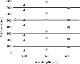
FIGURE 29.27 Phase unwrapping by the coincidence method.
The experimental apparatus is shown in Figure 29.28. Its optics consists of a white LED illumination unit and a color camera with a multi-bandpass filter inside, as shown in Figure 29.29.
The spectral transmittance of the filter is shown in Figure 29.30.
The central wavelengths are 470, 560, and 600 nm, and each of their bandwidths is 10 nm. The camera is an ordinary CMOS color camera with 640 × 480 pixels. Its spectral sensitivity is shown in Figure 29.31 for the wavelengths of the illumination.
The captured image was stored in a PC memory with a color depth of 24 bits per pixel. The color crosstalk was compensated by the crosstalk compensation algorithm reported in [28]. We wrote a program in the C language to implement the GMFT algorithm on the Windows PC.
In our experiments, a calibrated step wafer (Mikropack, Germany) was used, which consists of a 100 mm Si-wafer with six silicon dioxide (SiO2; n = 1.46) steps between 0 and 500 nm, as shown in the captured image (Figure 29.32).
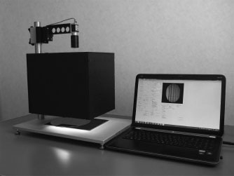
FIGURE 29.28 Experimental apparatus.
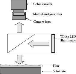
FIGURE 29.29 Optics of the experimental apparatus.
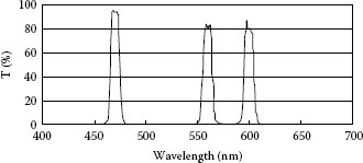
FIGURE 29.30 Spectral transmittance of the multi-bandpass filter.
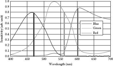
FIGURE 29.31 Spectral sensitivity of the color camera, with the three wavelengths used in the experiment.
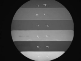
FIGURE 29.32 Captured color image of thickness standard, and 12 points for GMFT fitting (shown in white numbers).
The nonlinear least-squares equation in the GMFT algorithm was solved using the Davidon–Fletcher–Powell method [30]. There were 12 data points to be fitted, as shown in Figure 29.32. The initial thickness values were set to be the nominal values. The thickness range of each point was set to be the nominal value, ±50 nm.
In the second step, we calculated the thickness distribution over the whole 640 × 480 pixel area by using the parameters obtained in the first step.
From the 12-point intensity data, the corresponding thicknesses were estimated by the GMFT method. The results are shown in Table 29.1.
Then, the thickness distribution of the whole area was measured by the ACOS method. As shown in Figure 29.33, good agreement between the measured and predicted thickness distributions was obtained. Figure 29.34 shows a good correlation between the nominal and measured thicknesses.
The total calculation time for 640 × 480 pixels was about 220 ms, including 0.5 ms of the GMFT fitting using a C language program running on a Windows PC (2.5 GHz Intel Core i7 CPU).
TABLE 29.1
Results of GMFT Fitting
Variable Estimated |
Variable Estimated |
||
t(1) |
0 |
a(B) |
160 |
t(2) |
117 |
a(G) |
85 |
t(3) |
208 |
a(R) |
135 |
t(4) |
306 |
b(B) |
0.49 |
t(5) |
403 |
b(G) |
0.53 |
t(6) |
506 |
b(R) |
0.58 |
t(7) |
0 |
||
t(8) |
118 |
||
t(9) |
208 |
||
t(10) |
307 |
||
t(11) |
403 |
||
t(12) |
506 |
||
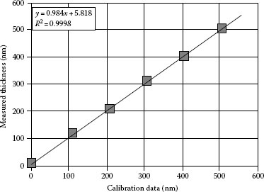
FIGURE 29.33 Estimated thickness profile by the ACOS method.
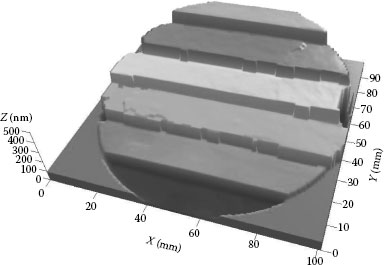
FIGURE 29.34 Correlation between the nominal and average estimated thicknesses of six areas.
29.6.4 EXAMPLES OF MEASUREMENTS
The thickness profile of an epitaxial film on a wafer was measured. The color image and the measured thickness profile are shown in Figure 29.35.
The thickness profiles of a down-flowing soap film were measured continuously. The time-series results are shown in Figure 29.36. The measurement speed was approximately 9 fps with the resolution of 160 × 120 pixels.
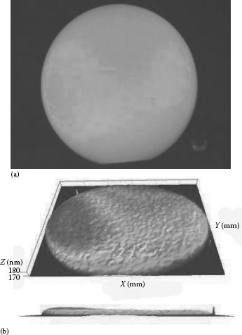
FIGURE 29.35 (a) Captured image and (b) estimated thickness profile of an epitaxial film on a wafer.
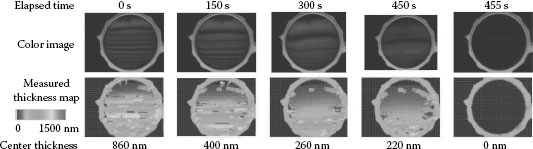
FIGURE 29.36 Time-series captured images and estimated thickness profiles of a flowing soap film.
The features of this technique include
•. Single-shot thickness distribution measurement
•. Low cost and simple optics
•. Wide measurement range of 20–8000 nm
•. Revolutionarily fast measurement speed of 2,000,000 pixels/s
•. Superior repeatability of 1 nm
•. No precalibration required
•. Vibration resistant
•. Applicable to moving objects
In this chapter, we presented five techniques to measure film thickness profiles using optical interferometry: (1) profiling of a thick transparent film, (2) profiling of a thin transparent film, (3) thickness profiling of a freestanding film, (4) simultaneous measurement of the thickness and refractive index of a freestanding film, and (5) thickness profiling by interference color analysis. All techniques are suitable for practical use.
Recent rapid advances in electronics and computer technology now allow the incorporation of newly developed, sophisticated algorithms in interferometric profilers, with dramatic results. These advances indicate the superb future potential of this technology and signal the beginning of a “second generation of interferometry.”
1. Caber, P.J., Interferometric profiler for rough surface, Applied Optics, 32, 3438, 1993.
2. Chim, S.S.C. and Kino, G.S., Three-dimensional image realization in interference microscopy, Applied Optics, 31, 2550, 1992.
3. Deck, L. and de Groot, P., High-speed non-contact profiler based on scanning white light interferometry, Applied Optics, 33, 7334, 1994.
4. Dändliker, R., Zimmermann, E., and Frosio, G., Electronically scanned white-light interferometry: A novel noise-resistant signal processing, Optics Letters, 17, 679, 1992.
5. Hirabayashi, A., Ogawa, H., and Kitagawa, K., Fast surface profiler by white-light interferometry by use of a new algorithm based on sampling theory, Applied Optics, 41, 4876, 2002.
6. Flournoy, P.A., McClure, R.W., and Wyntjes, G., White-light interferometric thickness gauge, Applied Optics, 11, 1907, 1972.
7. Tsuruta, T. and Ichihara, Y., Accurate measurement of lens thickness by using white-light fringes, Proc. ICO Conf. Opt. Methods in Sci. and Ind. Meas., Tokyo, Japan, p. 369372, 1974; Japanese Journal of Applied Physics, Supplement, 14-1, 369, 1975.
8. Lee, B.S. and Strand, T.C., Profilometry with a coherence scanning microscope, Applied Optics, 29, 3784, 1990.
9. Nakamura, O. and Toyoda, K., Coherence probing of the patterns under films, Kougaku, 21, 481, 1992 (in Japanese).
10. Itoh, M. et al., Broad-band light-wave correlation topography using wavelet transform, Optical Review, 2, 135, 1995.
11. Toray Inspection Equipment Home Page, Toray Engineering Co., 2013, http://www.scn.tv/user/torayins/.
12. Kitagawa, K., 3-D profiler of a transparent film using white-light interferometry, Proceedings of SICE Annual Conference 2004, Sapporo, Japan, p. 585, 2004.
13. Otsu, N., An automatic threshold selection method based on discriminant and least squares criteria, Transactions of IECE, 63-D, 349, 1980 (in Japanese).
14. Kim, S.W. and Kim, G.H., Thickness-profile measurement of transparent thin-film layers by white-light scanning interferometry, Applied Optics, 38, 5968, 1999.
15. Kim, D. et al., Fast thickness profile measurement using a peak detection method based on an acousto-optic tunable filter, Measurement Science and Technology, 13, L1, 2002.
16. Akiyama, H., Sasaki, O., and Suzuki, T., Sinusoidal wavelength-scanning interferometer using an acousto-optic tunable filter for measurement of thickness and surface profile of a thin film, Optics Express, 13, 10066, 2005.
17. Kitagawa, K., Film thickness profiling by interferometric optical path difference detection, Proceedings of DIA (Dynamic Image Processing for Real Application) WS 2007, Sapporo, Japan, p. 137, 2007 (in Japanese).
18. Kitagawa, K., Simultaneous measurement of refractive index and thickness of transparent films by white-light interferometry, Proceedings of JSPE Autumn Conference, 461, 2007 (in Japanese).
19. Kalliomaki, K.J. et al., U.S. Patent 4,647,205, 1987.
20. Fukano, T. and Yamaguchi, I., Simultaneous measurement of thicknesses and refractive indices of multiple layers by a low-coherence confocal interference microscope, Optics Letters, 21, 1942, 1996.
21. Maruyama, H. et al., Low-coherence interferometer system for the simultaneous measurement of refractive index and thickness, Applied Optics, 41, 1315, 2002.
22. Parthasarathy, S., Wolfe, D., Hu, E., Hackwood, S., and Beni, G., A color vision system for film thickness determination, Proceedings of IEEE Conference on Robotics and Automation, Vol. 4, p. 515, 1987.
23. Birnie, D., Optical video interpretation of interference colors from thin transparent films on silicon, Materials Letters 58, 2795, 2004.
24. Kubo, M., Ohtsubo, Y., Kawashima, N., and Marumo, H., Head slider flying height measurement using a color image processing technique, JSME International Journal, Series 3, 32, 264, 1989.
25. Hartl, M., Krupka, I., Poliscuk, R., and Liska, M., Computer-aided evaluation of chromatic interferograms, Proceedings of the Fifth International Conference in Central Europe on Computer Graphics and Visualization, Pizen, Czech Republic, p. 45, 1997.
26. Eguchi, M. and Yamamoto, T., Film thickness measurement using white light spacer interferometry and its calibration by HSV color space, Proceedings of the Fifth International Conference on Tribology, Parma, Italy, p. 20, 2006.
27. Kitagawa, K., Thin-film thickness profile measurement by three-wavelength interference color analysis, Applied Optics 52, 1998, 2013.
28. Kitagawa, K., Single-shot surface profiling by multi-wavelength interferometry without carrier fringe introduction, Journal of Electronic Imaging 21, 021107, 2012.
29. Kitagawa, K., Fast surface profiling by multi-wavelength single-shot interferometry, International Journal of Optomechatronics 4, 136, 2010.
30. Fletcher, R. and Powell, M.J.D., A rapidly convergent descent method for minimization, Computational Journal 6, 163, 1963.
31. Tilford, C., Analytical procedure for determining lengths from fractional fringes, Applied Optics 16, 1857, 1977.