
CONTENTS
3.2 Operating Principle of Optoelectronic Sensors
3.2.1 Conversion of Light to Electrons
3.3.1 Semiconductor Sensors for High-Light-Level Applications
3.3.2 Point Sensors for Low-Light-Level Applications
3.4 Multi-Pixel and Position-Sensitive Sensors
3.4.2 Position-Sensitive Sensors
3.5.2 Image Sensors and Cameras for Low-Light-Level Applications
3.6 X-Ray or Gamma-Ray Sensors
3.7 Selection Guide for Optoelectronic Sensors
Optoelectronic sensors detect electromagnetic radiations such as x-rays, ultraviolet (UV), visible, and infrared (IR) light, ranging from short to long wavelengths. These radiations are converted to electrons by the sensors and output as an electric current. The output current is generally amplified by an amplifier, converted to a digital number by an analog-to-digital converter (ADC), and recorded by a computer, for example. The optoelectronic sensors, the most essential part of this detection process, are discussed in this chapter.
This chapter is written to help readers select the most appropriate sensor for their application. To make a proper selection, readers must know the operating principles of optoelectronic sensors, which are discussed in Section 3.2, including the mechanisms for converting radiation to electrons and the spectral responses of sensors from UV to IR. Sections 3.3 through 3.5 discuss point sensors, multi-pixel/position-sensitive sensors, and image sensors, respectively, for the detection of UV–IR light. In each section, sensors with high gain of the order of 106 for low light level as well as those for high light level are described. Since x-rays behave differently from other lights, x-ray sensors are described in an independent section (Section 3.6). By the end of this chapter, readers should understand the need to take several factors into account such as spectral response, gain, and spatial and time resolutions for the selection of proper sensors, as shown in Figure 3.1. A selection guide to sensors is described in Section 3.7 instead of a summary of this chapter.
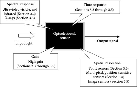
FIGURE 3.1 Critical factors in selecting an optoelectronic sensor discussed in this chapter for an application.
3.2 OPERATING PRINCIPLE OF OPTOELECTRONIC SENSORS
Optoelectronic sensors convert light information to electrical signal. Thus, the operation is based on a mechanism for converting light to an electric current. The mechanism and efficiency of the conversion are described in this section.
3.2.1 CONVERSION OF LIGHT TO ELECTRONS
Since the smallest units of light and electricity are expressed by a photon and an electron, respectively, we can describe the detection process in those terms. Photons are converted to electrons by optoelectronic sensors and measured as an electric current. More precisely, when a photon is absorbed in a semiconductor material, for example, an electron is excited from a valence band to a conduction band and extracted to a readout circuit as an output signal.
Three processes are used to extract electrons from materials: photovoltaic, photoconductive, and photoelectric effects. The photovoltaic effect occurs in a semiconductor sensor having p- and n-type regions facing each other to produce a p–n junction, as shown in Figure 3.2a. By absorbing photons, electrons are excited to a conduction band while holes are left behind in a valence band, thus generating electron–hole pairs. The electrons diffuse or drift in the material toward the p–n junction and eventually reach the n-type region due to a potential difference built between the n- and p-type regions, as shown in Figure 3.2b [1]. The holes, on the other hand, reach the p-type region because of their positive charge. As a result, an electric current is provided to the outer circuit. This type of optoelectronic sensor is called a photodiode (PD).
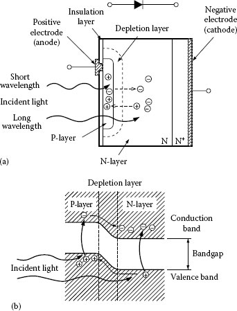
FIGURE 3.2 (a) Structure of a photodiode (PD) using photovoltaic effect. (b) In response to incident photons, electron–hole pairs are generated and separated by potential difference at the p–n junction to output a current to a readout circuit.
Because of its operating principle, a PD can detect photons having energy higher than the bandgap of the material, where the bandgap is the potential difference between the conduction and valence bands. The energy of a photon (E [J or eV]) can be described as a function of its wavelength (λ [m]) by the following formula:
where
h is Planck’s constant (6.6 × 10⁻³⁴ Js)
c is the speed of light (3.0 × 10⁸ m/s)
e is the charge of an electron (1.6 × 10⁻¹⁹ C)
In the case of silicon (Si), the most widely used material for PDs, photons of less than 1100 nm can be detected because Si’s bandgap is 1.1 eV. InGaAs or InSb is used for longer wavelengths in the IR because of its smaller bandgap. Spectral responses of sensors using these materials are discussed in Section 3.2.2.
The photoconductive effect also generates electron–hole pairs in a semiconductor material in response to incident photons. However, in this case, generated charges decrease the resistivity of the material. By applying a bias voltage to both ends of an effective area, the input light power can be measured as a variation of a current to a readout circuit, as shown in Figure 3.3 [2]. An optoelectronic sensor using the photoconductive effect is called a photoconductor, a photoconductive cell, or a photoresistor. Photoconductors made of materials with a small bandgap are mostly used to detect IR light.
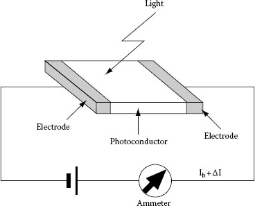
FIGURE 3.3 Schematic drawing of a sensor using photoconductive effect, which varies its resistivity in response to input light. Thus, input light power is measured by an electric current to the output circuit. (From Dakin, J.P. and Brown, R.G., Handbook of Optoelectronics, 1, Copyright 2006. Reproduced by permission of Taylor & Francis Group, LLC, a division of Informa plc, Boca Raton, FL.)
The photoelectric effect is an emission of electrons from a material to vacuum in response to input photons when the energy of the photon is larger than the work function of the material. The work function is a potential difference between Fermi and vacuum levels. Although the photoelectric effect occurs in pure metals such as gold (Au) or silver (Ag), the conversion efficiency from a photon to an electron is very low and limited to the UV region. Composite materials generally called photocathodes, which more readily convert photons to electrons, are used in sensors. An alkali–antimonide photocathode made of antimony (Sb) and alkali materials such as sodium (Na), potassium (K), and cesium (Cs) is fabricated on an input surface of a vacuum tube, as shown in Figure 3.4, to detect photons from UV to near-IR light. Photocathodes are used in photomultiplier tubes (PMTs) as discussed in Section 3.3.2.
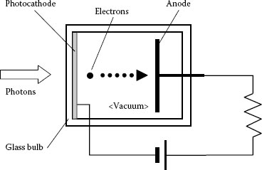
FIGURE 3.4 A phototube has a photocathode, where photoelectric effect occurs. Electrons emitted from the photocathode are received by an anode and output to a readout circuit.
As mentioned in the previous section, the conversion of photons to electrons is a key process in optoelectronic sensors. The conversion efficiency, which depends upon wavelength, is called a spectral response and expressed as quantum efficiency (QE). The spectral response is also described as radiant sensitivity, a ratio of the output current and the corresponding input light power. The QE (%) at a specific wavelength (λ [nm]) is related to the radiant sensitivity (S [A/W]) as shown in the following formula:
QEs of photovoltaic and photoelectric sensors for UV, visible, and near-IR regions are summarized in Figure 3.5 as a function of wavelength [1,3]. As shown in this figure, a Si-PD shows a QE of approximately 70% from UV to near-IR, whereas photocathodes are less sensitive than that because the emission probability of electrons to vacuum is small. Recently, the emission probability has been drastically improved, and a QE of 45% around 400 nm is achieved by an “ultra bialkali (UBA)” photocathode. GaAsP photocathodes made from semiconductor crystals reach a QE of 50% in the visible region, as shown in Figure 3.6 [4]. GaAs and InP/InGaAs photocathodes, as shown in the same figure, have high sensitivity in the near-IR region [5,6].
In the case of optoelectronic sensors for IR, D* (D-star) is generally used as a figure of merit to compare the sensitivity of different types of sensors such as PDs and photoconductors. D* is the sensitivity indicating the signal-to-noise ratio (S/N) for AC signal per unit light power, as shown in the following formula:
where
Δf (Hz) is the bandwidth of the output circuit
P (W/cm2) is the input light power density
A (cm2) is the effective area
D* values of several photoconductors and PDs are summarized in Figure 3.7 [7]. Spectral response of mercury cadmium telluride (MCT) depends on its composition, as shown here. The D* of a thermopile, which converts the energy of photons to heat and the variation of temperature is measured by a current, is shown as well.
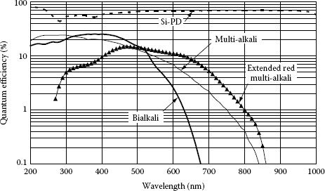
FIGURE 3.5 Spectral responses of a Si-PD (photovoltaic effect) and several photocathodes (photoelectric effect) from UV to near-IR region.
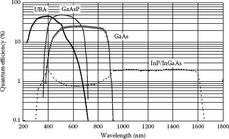
FIGURE 3.6 Spectral responses of new photocathodes, such as “ultra bialkali (UBA),” GaAsP, GaAs, and InP/InGaAs photocathodes.
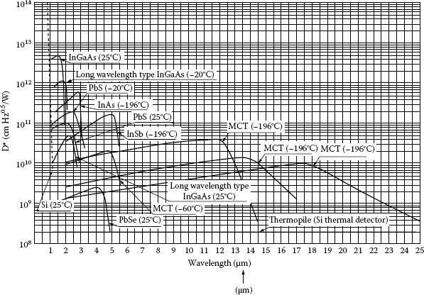
FIGURE 3.7 D* of PDs (photovoltaic effect) and photoconductors (photoconductive effect) with various compound materials are shown. D* is used to compare sensitivities of sensors for IR region.
A variety of optoelectronic sensors are available for a variety of applications. Point sensors are used for applications that do not require any position resolution. In this section, point sensors for low to high light levels and some electronics for these sensors are described.
3.3.1 SEMICONDUCTOR SENSORS FOR HIGH-LIGHT-LEVEL APPLICATIONS
For the detection of high light level, the most widely used optoelectronic sensor is a PD made of Si, which detects light from 200 to 1100 nm, as shown in Figure 3.5. Based on mature process technology, Si-PDs show a high QE of 70% in the visible region. Si-PDs with effective areas of up to 7.8 cm2 are available [8]. However, a smaller effective area is better in terms of dark current and response time. The response time (fall time), Tf (s), of a PD relates to the bandwidth, B (Hz), as expressed by the following equations:
where
R (Ω) is an impedance of a readout circuit
C (F) is the capacitance of a PD determined by the following equation:
where
ε0 is the electric constant (8.9 × 10⁻¹² F/m)
εr is a relative dielectric constant (11.9 for Si)
A (m2) is the effective area
d (m) is the thickness of the depletion layer
The smaller the effective area (A), the faster the time response (Tf). Another way to ensure fast time response is to increase the thickness of the depletion layer, and PIN-PDs are an example of this approach. PIN-PDs have a thick intrinsic (low impurity level) layer that is depleted readily to reduce the capacitance. The bandwidths of PIN-PDs are 1.0 GHz and 60 MHz for effective areas of 0.13 mm2 [9] and 13 mm2 [1], respectively.
Because of their stability, reliability, robustness, and price, varieties of Si-PDs are commercialized for various applications such as analytical instruments, medical, illuminometer, and academic research, as shown in Figure 3.8. Si-PDs are also used in cars for automatic head lights, automatic air conditioner, and automatic wipers.
For the detection of IR light whose wavelength is longer than 1000 nm, PDs and photoconductors made of various compound materials are used. Spectral response (D*) is determined by the material, as shown in Figure 3.7. InGaAs shows high sensitivity at wavelengths shorter than 2 μm, InSb is the best around 5 μm, and MCT shows the best D* at wavelengths longer than 5 μm. It is recommended to choose the material showing the highest D* at the wavelength of interest. In general, PDs show better D* and more stable operation than photoconductors. On the other hand, PDs require cooling to reduce dark current, making them more expensive than photoconductors. One of the major applications of IR sensors is in optical communication at 1.3 or 1.55 μm [10], where a loss of optical fiber is minimal. High-speed PDs made of InGaAs are used for this application. IR sensors are also used to measure temperature because thermal objects emit IR radiation [11]. Gas detection is another application in the IR region [11] because each gas has keen absorption in specific wavelengths depending upon its composition or a chemical bond.
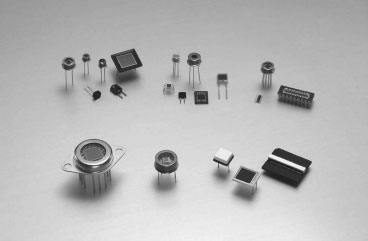
FIGURE 3.8 Si-PDs commercialized for various applications.
3.3.2 POINT SENSORS FOR LOW-LIGHT-LEVEL APPLICATIONS
It is very difficult for a PD to detect a single photon because one photon generates only one electron–hole pair in a sensor and the charge of an electron (1.6 × 10⁻¹⁹ C) is very small. An amplifier lowers the detection limit; however, it is still in the order of 108 photons/s as determined by the noise of the amplifier, assuming a noise of 1 pA/Hz0.5 at a bandwidth of 10 kHz. To lower the detection limit further, sensors should have an internal gain.
An avalanche photodiode (APD) is a sensor with internal gain [12]. As shown in Figure 3.9, the APD has a region of high electric field around the p–n junction where an avalanche multiplication occurs. In this region, charges are accelerated rapidly by a high electric field to produce another electron–hole pair upon interaction with other atoms. This phenomenon is called impact ionization, and successive occurrences lead to an avalanche multiplication. The impact ionization depends heavily on the electric field [13]; thus, the gain of an APD is determined by a bias voltage.
Since the ionization coefficient of an electron is much larger than a hole’s [13], Si-APDs are designed so that electrons, not holes, enter the avalanche region. APDs are used at the gain of less than 100 for stable operation, and temperature dependence of the gain should be considered during operation. Many Si-APDs are used as sensors for light detection and ranging, for example, where pulsed light is irradiated, and reflected light from an object is measured by an APD to determine the distance to the object. Large-area APDs, such as 5 × 5 mm, are used in high-energy physics experiments [14].
When a bias voltage to an APD is increased, leakage current starts to rise rapidly. This voltage is called a breakdown voltage, which is specified at the leakage current of 1 μA. APDs are generally used in a linear mode at voltages lower than the breakdown voltage, where an output current is linearly proportional to incident light power. However, APDs are sometimes used in Geiger mode [15], where a higher voltage than the breakdown voltage is applied, for photon counting. In this mode, an electron triggers an avalanche breakdown, which produces high output current to be detected. Since the avalanche breakdown causes damage to the APD, a bias circuit is designed to reduce the voltage to quench the breakdown by a resistor. An equivalent circuit explaining this detection process of Geiger-mode APD is schematically shown in Figure 3.10. Since dark current generated spontaneously at room temperature triggers the avalanche breakdown, cooling is necessary, and the effective diameter of the APD should be small, as small as 0.175 mm, to lower the dark count rate [16]. Owing to its photon-counting capability and high QE of 65% around 700 nm, Geiger-mode APDs are used for photon-counting applications in fluorescent measurement. According to the operating principle, only one pulse is output even when many photons arrive at the same time.
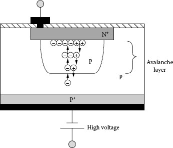
FIGURE 3.9 Schematic drawing of an APD having a high-electric-field region around the p–n junction, where avalanche multiplication occurs for internal gain.
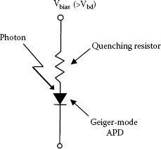
FIGURE 3.10 An equivalent circuit of Geiger-mode APD to detect single photons. Step 1: The bias voltage is set at larger than the breakdown voltage (Vbd). Step 2: When a photon arrives, avalanche breakdown occurs, and large pulse is output to the circuit. Step 3: A bias voltage is reduced at once by the quenching resistor to stop avalanche breakdown and returns to the original point waiting for the arrival of the next photon.
A new type of Geiger-mode APD capable of counting simultaneous photons, shown in Figure 3.11, has been developed [17]. This new sensor, called a “multi-pixel photon counter (MPPC)” [18] or a “silicon photomultiplier (Si-PM)” [19], has a large number of pixels constructed on a monolithic Si chip. Each pixel has its own quenching resistor. When two photons arrive at different pixels simultaneously, an output pulse twice as large as that for one photon is obtained. Thus, the number of incident photons can be measured, as shown in Figure 3.11. The linearity is limited by the number of pixels on a chip because the pulse height of output pulses starts saturating when more than one photon tends to hit one pixel at the same time. MPPCs with 1 × 1 mm and 3 × 3 mm effective area are available in the market with a pixel pitch from 25 to 100 μm. A 3 × 3 mm MPPC with pixel pitch of 25 μm has 14,400 pixels [18]. Because of its photon-counting capability and fast response time, MPPCs are suitable for high-energy physics experiments [20] and positron emission tomography (PET) [21]. Because MPPCs are also insensitive to high magnetic fields, they are especially suitable for magnetic resonance imaging PET.
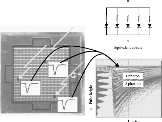
FIGURE 3.11 Operating principle of an MPPC, which consists of effective pixels that are connected to quenching resistors. When two photons arrive at different pixels simultaneously, an output pulse that is twice as large as that of a single photon appears on the output circuit; thus, the MPPC has both photon-counting capability and linearity.
In terms of photon counting, PMTs [3] are still the most commonly used optoelectronic sensors in various applications. In addition to a photocathode (shown in Figure 3.4), a PMT has dynodes in a vacuum tube to multiply electrons, as shown in Figure 3.12 [22].
In response to incident photons, electrons are emitted from the photocathode. The emitted electrons are then multiplied at each dynode by secondary electron multiplication, where a primary electron generates additional 5–10 electrons when striking a dynode. With 8 or 10 stages of dynodes, the total gain reaches 106–107, which is optimal to detect single photons. A typical gain characteristic of a PMT is shown in Figure 3.13 [22] as a function of a bias voltage. Contrary to Geiger-mode APDs, PMTs detect continuous light as well as pulsed light. Since the multiplication occurs in vacuum, temporal information of the input photon is not degraded. Typical rise and fall times of a PMT are 1 and 10 ns, respectively.
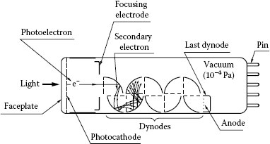
FIGURE 3.12 Sectional drawing of a PMT, which consists of a photocathode and dynodes in a vacuum tube. In response to incident photons, electrons are emitted from the photocathode and multiplied by the dynodes. Since each dynode multiplied electrons by a factor of 5–10, the gain reaches 106–107 in total, high enough to detect single photons.
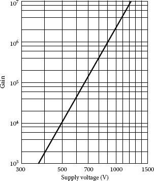
FIGURE 3.13 Typical gain characteristics of a PMT as a function of bias voltage.
In addition to high gain and fast time response, PMTs with a large effective diameter (up to 500 mm) are available at a reasonable price. A low dark count of 0.01–0.1 count/s/mm2 or 1.6 × 10⁻²¹ to 1.6 × 10⁻²² A/mm2 for bialkali photocathodes is another feature of PMTs. In general, QEs of photocathodes are lower than those of sensors using the photovoltaic effect as shown in Figure 3.5. However, a drastic improvement in QE is achieved in a “UBA” and a semiconductor crystal photocathode, reaching QEs of approximately 50%, as discussed in Section 3.2.2.
As shown in Figure 3.14 [22], PMTs with various photocathode materials, shapes (round, square, hexagonal), and dynode structures are commercialized for various low-light-level applications.
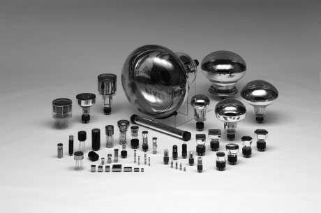
FIGURE 3.14 PMTs are designed with various photocathode materials, shapes, and dynode structures for various applications.
In general, PMTs are bulkier than semiconductor sensors; however, a “flat panel PMT” is available in the market [23]. Because of “metal-channel dynodes” made of thin metal plates, the outer dimension of this PMT is 52 × 52 × 15 mm, thinner than any other PMTs. The flat panel PMT is discussed in Section 3.4.1 in detail. PMTs are typically used in analytical instruments like spectrometers [24], in biology and medical fields to detect fluorescent light [25,26], and in medical imaging such as PET [27] and gamma cameras [28]. Now PMTs can also be used for portable instruments, such as micro-total analysis systems (μTAS) and environmental monitors, due to a significant reduction in detector size. A fusion of micro-electro-mechanical systems and vacuum technology, a miniaturized PMT with outer dimensions of 13 × 10 × 2 mm, and a 1 × 3 mm bialkali photocathode has been commercialized, as shown in Figure 3.15 [29]. Even with this small body, a gain of 106 and time response in the nanoseconds range are obtained.
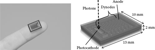
FIGURE 3.15 A miniaturized PMT on a fingertip appeals high performance, not compromised for its small size.
A hybrid photodetector (HPD) is another optoelectronic sensor that detects single photons. Instead of dynodes, the HPD has a Si avalanche diode (AD) to multiply electrons, as shown in Figure 3.16 [30]. Electrons emitted from the photocathode are accelerated up to 8 keV and are focused onto the AD. Then, an electron deposits its kinetic energy and generates approximately 1000 electron–hole pairs in Si; this is called electron-bombarded gain. The electrons generated in the AD drift toward the p–n junction for avalanche multiplication; thus, the total gain of the HPD reaches 105. Due to the large electron-bombarded gain, the noise figure of electron multiplication is almost ideal, close to one; thus, the S/N is quite high. This is why the HPD can distinguish up to five electrons by its output pulse height, as shown in Figure 3.17. An HPD incorporating a small AD shows faster response time than conventional PMTs [30,31]; the rise and fall times are 400 ps, and the timing resolution for a single photon is less than 90 ps. In addition to good timing resolution, the HPD shows a small probability of afterpulsing, a false signal triggered by the real signal and appearing a certain period after the real signal. Smaller afterpulsing than PMTs and Geiger-mode APDs makes HPDs attractive for use in fluorescence correlation spectroscopy and time-correlated single-photon counting (TCSPC) [32,33].
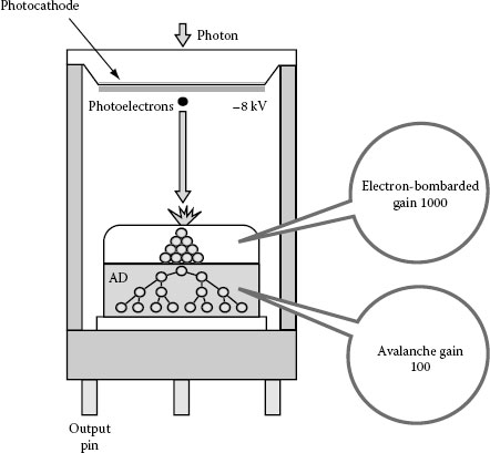
FIGURE 3.16 An operating principle of an HPD is shown, where electrons from the photocathode are accelerated and focused on the AD to make an electron-bombarded gain of 1000. The electrons are further multiplied by avalanche multiplication for a total gain of 105, high enough to detect single photons.
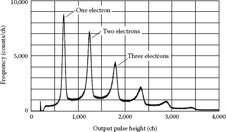
FIGURE 3.17 Pulse height spectrum of an HPD for irradiation of several photons to the photocathode on average. Several peaks corresponding to one, two, and three electrons from the photocathode are clearly observed.
Outputs of optoelectronic sensors should be recorded for analysis. Recording methods are discussed here for recording a waveform, counting photons, measuring a pulse-height spectrum, and timing of the arrival of photons.
To record a waveform, a current-to-voltage amplifier or a transimpedance amplifier is used for front-end electronics to feed voltage signal to an ADC. The ADC digitizes the signal, and a computer records it, as shown in Figure 3.18a. A digital oscilloscope works this way.
To count photons, a high-speed AC-coupled amplifier is used as front-end electronics to distinguish arriving photons individually. The output signal is compared to a threshold level by a comparator, and a number of output pulses are measured by a counter, as shown in Figure 3.18b.
The intensity of pulsed light is measured with a charge-sensitive amplifier, which accumulates input charge for a certain period and converts it to voltage. The output is further amplified and shaped by a shaping amplifier, and recorded by a multichannel analyzer, as shown in Figure 3.18c. The result obtained by this method is called a pulse height spectrum, as shown in Figure 3.17.
It is very useful to time the arrival of photons because the timing resolution of optoelectronic sensors is roughly 1/10th of the rise and fall times of the sensors. TCSPC uses this method to achieve time resolution in the order of 10 ps and a wide dynamic range of five orders [33]. To measure the timing of each photon, the output pulse of a high-speed amplifier is fed to a constant fraction discriminator (CFD), which outputs timing signal accurately even though pulse height fluctuates. The output signal of the CFD and trigger output of the light source are used for the start and stop signals, respectively, of a time-to-amplitude converter (TAC), where the TAC’s output is proportional to the time difference between start and stop signals. The output signal from the TAC is analyzed and recorded by a multichannel analyzer, as shown in Figure 3.18d.
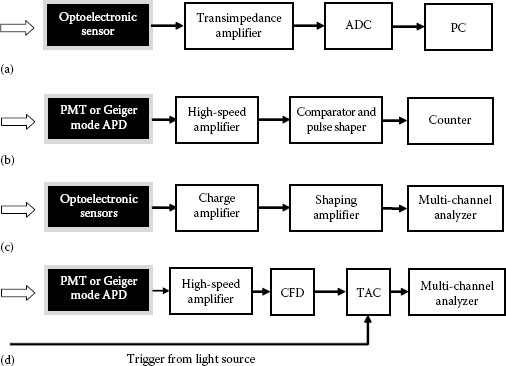
FIGURE 3.18 Readout electronics recording methods of signal from optoelectronic sensors for (a) recording waveform, (b) counting photons, (c) measuring pulse height spectrum, and (d) timing of the arrival of photons.
3.4 MULTI-PIXEL AND POSITION-SENSITIVE SENSORS
In the case of measuring multiple wavelengths or spectrum of light, multi-pixel sensors are required to measure them all at once; otherwise, it is necessary to scan the wavelength over a slit to be detected by a point sensor. On the other hand, for trigonometry, position-sensitive sensors are useful in measuring the position of a spot of light. In this section, multi-pixel sensors and position-sensitive sensors are discussed.
Semiconductor sensors with plural pixels are easy to design and fabricate by a semiconductor process. A variety of multi-pixel Si sensors linearly arranged from 2 to 46 pixels are available in the market. An example shown in Figure 3.19 has a 46-pixel array of 0.9 × 4.4 mm [34]. A 2D array of 2 × 2 pixels (2.5 × 2.5 mm/pixel) is also available [35]. For near-IR light, InGaAs array sensors up to 16 pixels (0.45 × 1 mm) [36] can be used. These are some examples of multi-pixel sensors for high light level, which are mostly used for spectrometers. Any modifications on number, size, and shape of pixels are technically possible.
One of the merits of multi-pixel sensors is high-speed readout because the signal from each pixel is read out in parallel. However, the parallel readout is sometimes a demerit because the complexity of readout electronics is proportional to the number of pixels. For more than 100 pixels, specifically designed complementary metal-oxide semiconductor (CMOS) readout electronics are used to read out every pixel sequentially. In this case, readout speed of whole pixels is limited. The multi-pixel sensors with CMOS readout electronics are categorized as image sensors and discussed in Section 3.5.1.
For low light level, multi-pixel PMTs with special dynodes called “metal-channel dynodes” [3] are used. Metal-channel dynodes, bars of thin metal shaped somewhat like the letter “S,” are arranged in rows and stacked on top of each other (with a pitch as small as 0.5–1 mm) to create channels for multiplied electrons, as shown in Figure 3.20. Electrons from the photocathode are multiplied in the dynodes while preserving their position information and are output from plural anodes located behind the dynodes; thus, a multi-pixel sensor is realized. Flat panel PMT with metal-channel dynodes is shown in Figure 3.20 [23]. This PMT has 16 × 16 (256 in total) anodes with an effective area of 49 × 49 mm. The PMT is very thin, just 15 mm thick, owing to the metal-channel dynodes. Because of their high speed and high gain, multi-pixel PMTs are used in spectrometers for confocal microscopes [37] and high-energy physics experiments [38].
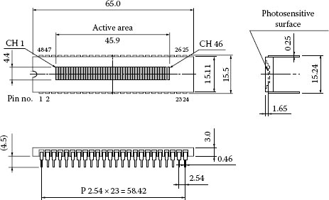
FIGURE 3.19 Dimensional outline of 46-linear array of Si-PD [34]. Size of each pixel is 0.9 × 4.4 (mm).
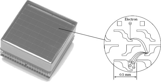
FIGURE 3.20 Photograph of a “flat panel PMT” and the structure of “metal-channel dynodes.”
3.4.2 POSITION-SENSITIVE SENSORS
A trigonometry is used to measure distance for auto-focusing of a camera, for example. As shown in Figure 3.21 [11], this system needs to measure the position of a spot light on a sensor; thus, a position-sensitive detector (PSD), shown in Figure 3.22 [39], with a resistive layer (p-layer) and two output terminals at both ends, is used. An irradiated position (x, from the center) is determined by the following equation:
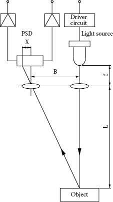
FIGURE 3.21 Schematic drawing of a trigonometry to measure distance, where an irradiated position is measured by a PSD.
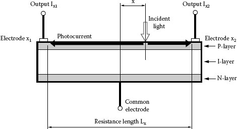
FIGURE 3.22 Sectional drawing of a one-dimensional PSD, having resistive layer (p-layer) and two terminals at both ends. An irradiated position is determined by the ratio of output currents from the terminals.
where
Lx is the length of the effective area
Ix1 and Ix2 are output currents from both terminals
Because of its operating principle, a small spot of less than 200 μm is required to irradiate PSDs. One-dimensional-type PSDs are available with effective lengths up to 37 mm [39]. A 2D type works in the same manner and up to 14 × 14 mm are available in the market [39]. One of the merits of PSDs is a good position resolution of 10 μm at a response time in the order of 1 MHz. These are achieved because signals from just two terminals are read out for one dimension and four terminals for two dimensions. It is more difficult to determine the position of a spot light using multi-pixel sensors or image sensors at these resolutions in position and time. It is worth noting that the response time and the position resolution depend upon the size, resistivity, and structure of the PSD as well as power and wavelength of the input light.
For low light level, multi-pixel PMTs are used as position-sensitive sensors by connecting each anode with resistors [40], as shown in Figure 3.23. The output current splits to four terminals through the resistor chain according to Equation 3.7. Thus, the irradiated position is determined. Putting segmented scintillator on a faceplate, a PMT with 16 × 16 pixels and a resistor chain are used for the state-of-the-art PET scanner [41].
To capture fine images, a large number of pixels—more than 250,000 pixels in general—are required. Then, some electronics are necessary to read out the signal of each pixel sequentially because parallel readout is impossible for so many pixels. Optoelectronic sensors having sequential-readout electronics are categorized as image sensors in this chapter and discussed in this section.
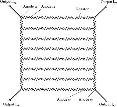
FIGURE 3.23 Resistor chain of 8 × 8 pixel PMT for position-sensitive operation.
Historically, there have been plenty of image sensors starting from image pickup tubes. However, two types of image sensors are mainly used today. One is a charge-coupled device (CCD), and the other is a CMOS image sensor.
A CCD has many light-sensitive and charge-transfer pixels monolithically, where charges are transferred from one pixel to the next one, like a bucket relay. Figure 3.24a [42] schematically shows the structure of an interline transfer CCD. Plenty of PDs work as light-sensitive pixels, converting incident photons to electrons and accumulating them. After an exposure time of 33 ms, for example, for TV-rate operation, charges in each PD are transferred to the charge transfer pixels (vertical shift register) nearby in a short time for readout. In a readout procedure, the charges are transferred one line down toward the horizontal shift register followed by repetitive transfers in horizontal shift registers to the readout circuit. Repeating this process achieves readout of all pixels. While reading out, signals for the next frame are accumulated in the PDs. Interline CCDs are used in scientific applications due to their performance and reasonable cost; however, sensitivity is limited because about half of the area is used for the charge transfer and thus insensitive to photons. Micro-lenses fabricated on PDs help to collect light [42], but the sensitivity is not as high as back-illuminated CCDs as discussed in Section 3.5.2.
The structure of another type of CCD, a frame transfer CCD, is shown in Figure 3.24b [42]. The effective area consists of a transparent shift register; thus, photons are converted to electrons in Si below the register. Once charges are accumulated, they are transferred vertically to the storage area in a very short time, from which charges are read out sequentially as described in interline CCDs. The frame transfer structure is used for a back-illuminated CCD and an electron-multiplying CCD as discussed in Section 3.5.2.
CMOS image sensors, on the other hand, consist primarily of plural PDs as light-sensitive pixels and MOS transistors that act as switches, turning on/off the connection between each PD and the readout circuit, as shown in Figure 3.25 [43]. A control circuit (vertical and horizontal shift registers) is fabricated monolithically on a chip to switch MOS transistors properly for sequential readout. Recently, an active pixel sensor having not only a switch but also an amplifier for each pixel is commonly used both to reduce noise and to increase frame rate [44]. The advantages of CMOS image sensors compared to CCDs are as follows:
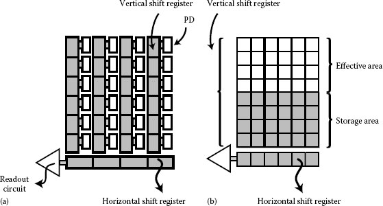
FIGURE 3.24 (a) A pixel layout of an interline-transfer CCD, where plural PDs accumulate charges, while CCDs (vertical and horizontal shift registers) transfer the charges. (b) Pixel layout of a frame-transfer CCD, where vertical transfer from effective area to storage area is carried out in a very short period, followed by a pixel-to-pixel readout from storage area.
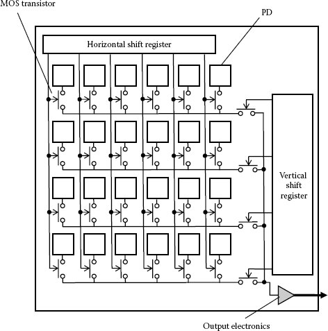
FIGURE 3.25 Schematic drawing of CMOS image sensor, where MOS transistors act as switches to connect PDs sequentially to the output electronics for readout.
1. The fabrication process is simple.
2. All electronics necessary for operation are fabricated monolithically, making operation simple.
3. Power consumption is low.
These are the reasons why CMOS image sensors are widely used in digital cameras and cell phones. In scientific applications, a CCD was a main player for a long time because of its high sensitivity and low noise. However, a scientific CMOS described in the following section is taking over the position. For practical use, an image sensor is assembled as a camera and generally connected to a computer for recording and analyzing images.
3.5.2 IMAGE SENSORS AND CAMERAS FOR LOW-LIGHT-LEVEL APPLICATIONS
CCDs can be used for low-light-level imaging with some modifications. Since the detection limit at low light levels is determined by an S/N, increasing the signal is essential and simple to achieve. Signals can be increased by improving QE or extending the exposure time. Back-illuminated CCDs help to increase signal due to improved QE. In a front-illuminated CCD, as shown in Figure 3.26 [45], photons enter the Si substrate through shift registers (polysilicon electrodes), which absorb or reflect part of the incident photons. As a result, the QE is 40% at the peak wavelength and zero below 400 nm, as shown in Figure 3.27 [46]. On the other hand, the back-illuminated CCD shows almost ideal spectral response, shown in the same figure, because there is nothing but effective Si layer on the back. Manufacturing the back-illuminated CCD requires a complicated process to thin the substrate down to approximately 10 μm. Thinning is necessary for high spatial resolution; otherwise, electrons generated at the back surface split to the neighboring pixels while they diffuse to the front surface for transfer.
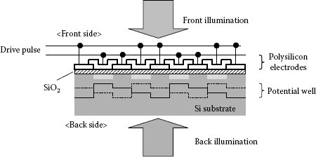
FIGURE 3.26 Sectional drawing of a frame-transfer CCD for front and back illumination, where the front surface is the processed surface with layers of polysilicon electrodes (shift registers), which absorb and reflect part of incident light. (From Dakin, J.P. and Brown, R.G., Handbook of Optoelectronics, 1, Copyright 2006. Reproduced by permission of Taylor & Francis Group, LLC, a division of Informa plc, Boca Raton, FL.)
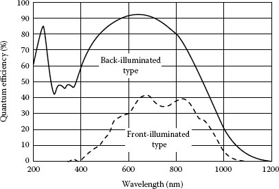
FIGURE 3.27 Spectral responses of front- and back-illuminated CCDs. The back-illuminated CCD shows high QE of 90% in visible region.
The other method to increase signal is to extend the exposure time. However, the dark current of a CCD is accumulated as well and generates noise. Cooling is useful to decrease the dark current because cooling of every 20°C decreases the dark current by one order of magnitude. Therefore, the lower the temperature, the better in terms of the dark current, as shown in Figure 3.28 [42]. To achieve a minimum temperature of −90°C, a CCD and a Peltier cooler are packed in a vacuum chamber, as shown in Figure 3.29 [42]. Various cooled CCDs are supplied as cameras in the market.
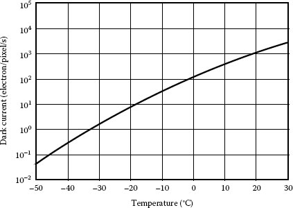
FIGURE 3.28 A dark current of a CCD as a function of temperature, where the dark current is decreased to 1/10th with cooling of every 20°.
A cooled CCD camera with long exposure time cannot be used to observe dim and fast-moving objects such as specimen under a microscope, for example. The solutions to this problem are either to get an internal gain in a sensor or to reduce noise further. In the case of Si, the impact ionization discussed in Section 3.3.2 can be used to obtain a gain. An electron-multiplying CCD (EM-CCD) uses this effect at the multiplier register by applying enough high voltage to the transfer gates, as shown in Figure 3.30 [42]. Although the gain of each transfer is small (such as 1.05), the total gain after 500 transfers reaches 1000. Cooling should be carried out the same way as a cooled CCD because dark current is also multiplied at the registers.
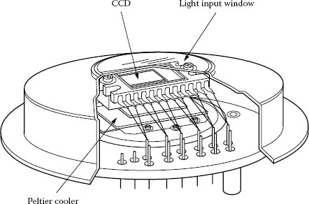
FIGURE 3.29 A vacuum chamber containing a CCD and a Peltier cooler to cool the CCD down to −90°C.
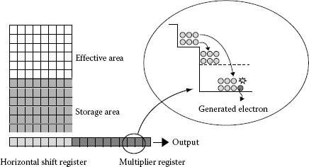
FIGURE 3.30 Structure of an EM-CCD to obtain gain at multiplier resistors by impact ionization.
The other approach to get a better image at short exposure times is to reduce noise by using a CMOS sensor whose every column has its own readout circuit, as shown in Figure 3.31 [43]. Because there are thousands of readout circuits, the bandwidth of each circuit could be reduced to make the readout noise less than 2 electrons (root mean square), which is one-fifth or less of a CCD’s readout noise. Furthermore, the S/N is readily preserved because the signal is digitized by an on-chip ADC. The additions of readout circuits and ADC are made possible by state-of-the-art CMOS technology that shrinks the feature size and allows the fabrication of circuits on silicon. This type of CMOS image sensor is called scientific CMOS (sCMOS), and its development has expanded CMOS applications to include scientific fields [47,48].
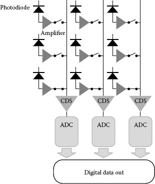
FIGURE 3.31 Structure of sCMOS, where a correlated double sampling (CDS) reducing electrical noise and ADC are fabricated; thus, digital signal is output from the sensor.
Another method to obtain a high gain is to combine a conventional CCD with an image intensifier. As shown in Figure 3.32 [49], the image intensifier consists of a photocathode, a microchannel plate (MCP), and a phosphor screen. An MCP is a thin glass plate with millions of small through-holes whose diameter is typically 6 μm and the thickness is 300 μm, as schematically shown in Figure 3.33 [50]. By applying bias voltage of typically 1 kV between the input and output surfaces of the MCP, incident electrons are multiplied by successive secondary electron multiplication while preserving their position information within a hole.
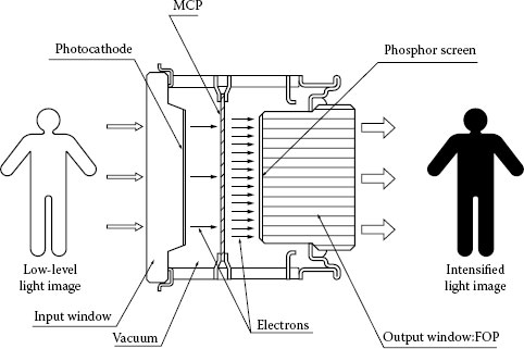
FIGURE 3.32 Structure and operating principle of an image intensifier is shown, where electrons emitted from the photocathode are multiplied by a factor of 1000 at the MCP; thus, input light image is intensified.
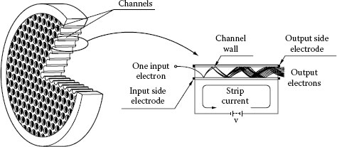
FIGURE 3.33 Schematic drawing of an MCP, which is a thin glass plate with a multitude of through holes. By applying voltage between the input and output surfaces, electrons are multiplied within the holes by a factor of 1000.
A proximity-focused structure preserves the spatial information of electrons entering the MCP, where electrons are multiplied by a factor of 1000. The multiplied electrons are accelerated and strike the phosphor screen to emit light. Thus, the input image is intensified. The output image is connected to a CCD through a fiber-optic plate (FOP) [51], a glass plate made of a bundle of optical fibers, which transmits the image while preserving spatial information. The coupling of images by an FOP shows better efficiency by one order of magnitude than that by a lens. This type of imaging system is called an intensified CCD (I-CCD). Using two layers of MCPs, the gain reaches 105. This gain value makes I-CCDs suitable for single-photon counting. Another feature is a very short exposure time (in nanoseconds) controlled by a gating operation, where a short forward bias voltage corresponding to the exposure time is applied between the photocathode and the MCP. In response to incident light image, an electron image is emitted from the photocathode.
Short exposure time is available with gate-operated I-CCDs. However, a CCD camera’s frame rate is still limited, typically 30 frame per second (fps). For higher frame rates, a specially designed CMOS image sensor similar to sCMOS with multiple output terminals is used. A C-MOS sensor with 512 output terminals and ADCs sharing light-sensitive pixels is reported [52] for this purpose. Then, parallel readout is carried out at 2 mega-pixels/s for each output terminal; thus, approximately 3500 fps is available with 512 × 512 pixels. In the market, 12,500 fps with 1024 × 1024 pixels is available [53]. Since a short exposure time means a very small number of photons per frame, an image intensifier is coupled to a C-MOS sensor to intensify light in many applications such as fluorescence microscopy [54].
A multi-port CCD [55] is another solution for high-speed imaging. However, this sensor is mostly used for time-delayed integration (TDI). In TDI operation, the CCD performs vertical transfer of charges repeatedly while matching the speed of images. Thus, charges are integrated, and their spatial information is preserved while moving on the CCD and finally read out, as shown in Figure 3.34 [55]. In this way, the TDI-CCD acts as a line sensor with extremely high sensitivity. Since the vertical transfer rate is limited by the pixel readout rate, a multi-port is useful to speed up the transfer. A TDI-CCD with 16 terminals for 2048 horizontal pixels is available, as shown in Figure 3.35 [55]. Since this CCD has output terminals in both upper and lower ends, bidirectional operation transferring charges both upward and downward is available.
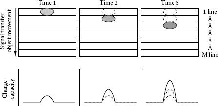
FIGURE 3.34 An operating principle of a TDI-CCD is shown, where the speed of vertical transfer of charges matches that of objects; thus, charges are integrated while transferring.
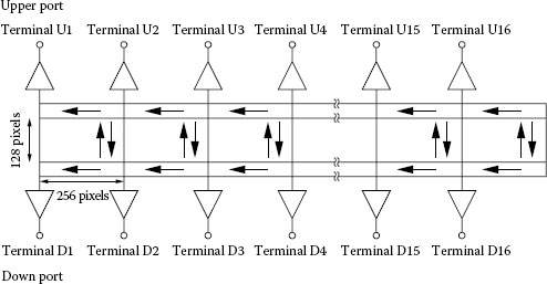
FIGURE 3.35 A pixel layout of TDI-CCD having 16 terminals for high throughput.
3.6 X-RAY OR GAMMA-RAY SENSORS
An x-ray or a gamma ray is also an electromagnetic radiation with a much shorter wavelength than UV photons, shorter than 10 nm. X-rays behave differently from the other photons: they transmit through materials easily or generate a lot of electron–hole pairs when absorbed. In this section, the physics for detecting x-rays and practical sensors are described.
To detect x-rays, they must first be absorbed by a material. The transmission characteristic of x-rays should be taken into account because transmission through a material depends heavily on an x-ray’s energy. As an example, the absorption characteristics of x-rays by Si are shown in Figure 3.36 as a parameter of thickness. This indicates that Si with a thickness of 0.5 mm absorbs x-rays of lower than 20 keV efficiently, meaning Si is sensitive only for low-energy x-rays. Once an x-ray is absorbed by Si, an electron having almost the same energy as that of the incident x-ray is generated, deposits its energy in Si, and generates a number of electron–hole pairs depending upon the energy of the x-ray (Ex [eV]). The average number (Neh) of generated electron–hole pairs is calculated according to the following equation:
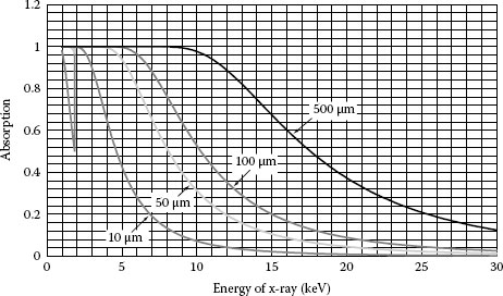
FIGURE 3.36 Absorption characteristics of x-rays by Si are shown as a parameter of the thickness.
where Eeh (eV) is the average energy needed to generate one electron–hole pair in a material. For Si, Eeh is 3.6 eV. The generated charges can be read out in the same way as a PD or a CCD. It is worth noting that x-rays are commonly expressed not by wavelength but by energy. Use Equation 3.1 to convert between energy and wavelength.
To absorb high-energy x-rays, specially designed lithium (Li)-drifted Si or germanium (Ge) detectors with a thick substrate are used [56]. They show excellent energy resolution for incident x-rays. However, they are not easy to use because cooling at liquid nitrogen temperature (-196°C) is required. Cadmium tellurium (CdTe) sensor is reported to be operated at room temperature [57] for small gamma cameras [58].
Another—and the most common solution—for the detection of high-energy x-rays is a combination of a scintillator and an optoelectronic sensor. Scintillators are made of materials with high atomic number and density, thus suitable to absorb high-energy x-rays. In a scintillator, an x-ray is converted to an electron with high kinetic energy, which excites many other electrons when depositing its energy. When relaxed, these electrons emit photons in the visible region to be detected by an optoelectronic sensor. Table 3.1 [59] lists several scintillators available in the market and includes their composition, density, decay time, emission wavelength, and major applications.
TABLE 3.1 Characteristics and Typical Applications of Scintillators
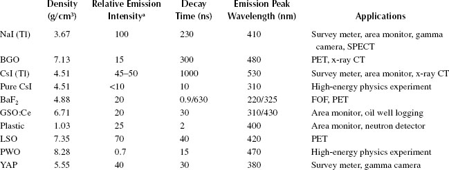
Source: Dakin, J.P. and Brown, R.G., Handbook of Optoelectronics, 1, Copyright 2006. Reproduced by permission of Taylor & Francis Group, LLC, a division of Informa plc, Boca Raton, FL.
a Normalized to NaI(Tl) as 1000.
A practical point sensor for x-rays consists of a scintillator and a PMT, as shown in Figure 3.37 [3].
A single x-ray photon is detected with this system because of the high sensitivity of a PMT. Since the number of emitted photons is proportional to the energy of the x-ray, the energy can be analyzed by the pulse height obtained by the readout electronics shown in Figure 3.18c. This type of sensor is widely used for a scintillation counter. A PET scanner [27] or a gamma camera [28] also uses a combination of a scintillator and a PMT. On the other hand, PDs are widely used to receive light from a scintillator, for example, for x-ray CT, when single-photon sensitivity is not required.
For imaging, scintillation light can be observed by a CCD camera through a lens [60], as shown in Figure 3.38, and the scintillator is deposited, for example, on an amorphous carbon plate [61]. This system is called CCD-digital radiography (CCD-DR). To improve coupling efficiency of light by the lens, a large C-MOS image sensor has been developed to receive the light from the scintillator through an FOP, as shown in Figure 3.39 [62]. This sensor is mechanically thin and distortion free without a lens, and this sensor is used for medical radiology. An x-ray image intensifier (x-ray II), another sensor, uses a photocathode directly coupled to a scintillator deposited on a faceplate, as shown in Figure 3.40 [63]. In response to x-rays, the scintillator emits photons, which are converted to electrons by the photocathode. Electrons from the photocathode are accelerated, reduced by a factor of 5, and focused on a phosphor screen to be read out by a CCD camera. The x-ray II shows the best sensitivity because of its efficient optical coupling to the photocathode and a gain of the conversion at the phosphor screen. Demerits are its large size (including a readout camera) and the distortion caused by an electron lens. X-ray IIs are used for medical imaging and nondestructive inspection. Since optics for x-rays are still not available for practical use, x-ray image sensors are relatively large, such as 125 × 125 mm for C-MOS image sensors [62] and 73 × 55 mm for x-ray IIs [63].
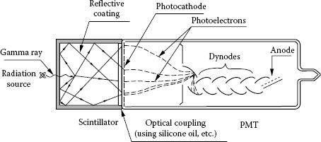
FIGURE 3.37 Configuration for scintillation counting, where a scintillator converts gamma rays to light to be detected by a PMT.
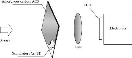
FIGURE 3.38 An imaging system for radiography consists of a scintillator on an amorphous carbon plate and CCD camera coupled by a lens.
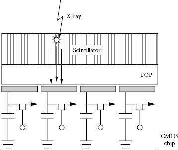
FIGURE 3.39 A high-sensitive sensor for radiography, where a scintillator is deposited on an FOP coupled to a C-MOS image sensor.
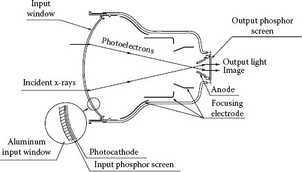
FIGURE 3.40 Configuration of an x-ray image intensifier, where x-rays are converted to light by a scintillator deposited on a photocathode. Electrons from the photocathode are demagnified and focused on a phosphor screen to be detected by a CCD camera.
3.7 SELECTION GUIDE FOR OPTOELECTRONIC SENSORS
As an alternative to a summary of this chapter, this section describes how to select the most appropriate sensor for each application:
1. Specify the wavelength of light to be detected. Refer to Section 3.2.2 for spectral responses for UV to IR and Section 3.6 for x-rays. Select the best one in terms of sensitivity.
2. Specify position resolution. Select a point sensor, a multi-pixel/position-sensitive sensor, or an image sensor, described in Sections 3.3 through 3.5, respectively.
3. Check the power of incident light. Sensors for high light and low light levels are described in Sections 3.3 through 3.5 as well.
4. Specify the response time. Point and multi-pixel sensors have fast time response as mentioned in Sections 3.3 and 3.4, whereas image sensors are slow in general. High-speed cameras are available as described in Section 3.5.3.
Figure 3.41 categorizes every sensor by wavelength and number of pixels. In each bold box, sensors in the upper left have high sensitivity and fast response, while those in lower right have low sensitivity and slow response. For optical measurement, selection of the most appropriate sensor for your application is the first step, and this chapter helps in the selection.
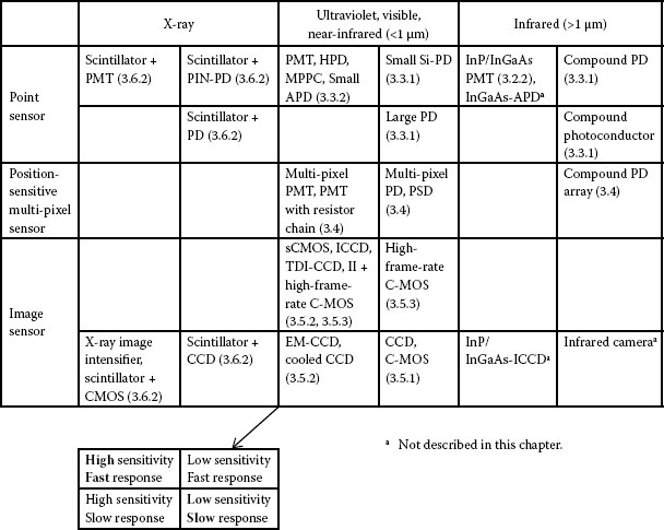
FIGURE 3.41 Photon sensors categorized by wavelength and number of pixels.
1. Si Photodiodes, Catalogue of Hamamatsu Photonics K.K., 2011.
2. Dakin, J. P. and Brown, R. G. W., Handbook of Optoelectronics, Taylor & Francis, Boca Raton, FL, Vol. 1, 418, 2006.
3. Hakamata, T. et al., Photomultiplier Tubes: Basics and Applications, 3rd edn., Hamamatsu Photonics K.K., Hamamatsu City, Japan, 2006.
4. Suyama, M., PoS (PD07), http://pos.sissa.it/archive/conferences/051/018/PD07_018.pdf (accessed January, 2007).
5. Niigaki, M. et al., Field-assisted photoemission from InP/InGaAsP photocathode with p/n junction, Appl. Phys. Lett., 71(17), 2439, 1997.
6. NIR Photomultiplier Tubes, Catalogue of Hamamatsu Photonics K.K., 2005.
7. Infrared Detectors, Catalogue of Hamamatsu Photonics K.K., 2013.
8. Si PIN photodiode, S3204/S3584 Series, Catalogue of Hamamatsu Photonics K.K., 2012.
9. Si PIN photodiode, S5751, S5752, S5973 Series, Catalogue of Hamamatsu Photonics K.K., 2012.
10. Optical Communication Device, Catalogue of Hamamatsu Photonics K.K., 2008.
11. Yamamoto, K. et al., Handbook of Optoelectronic Devices, Hamamatsu Photonics K.K., Hamamatsu City, Japan, 2004 (in Japanese) https://www.hamamatsu.com/resources/pdf/ssd/e06_handbook_compound_semiconductor.pdf (accessed November 26, 2014).
12. McIntyre, R. J., Recent developments in silicon avalanche photodiodes, Measurement, 3(4), 146, 1985.
13. Sze, S. M., Physics of Semiconductor Devices, 2nd edn., Wiley-Interscience, New York, Vol. 47, 1981.
14. Organtini, G., Avalanche photodiodes for the CMS electromagnetic calorimeter, IEEE Trans. Nucl. Sci., 46(3), 243, 1999.
15. Cova, S., Ripamonti, G., and Lacaita, A., Avalanche semiconductor detector for single optical photons with a time resolution of 60 ps, Nucl. Instrum. Methods, A253, 482, 1987.
16. SPCM-AQR, Catalogue of Perkin Elmer.
17. Golovin, V. and Saveliev, V., Novel type of avalanche photodetector with Geiger mode operation, Nucl. Instrum. Methods, A518, 560, 2004.
18. MPPC, Catalogue of Hamamatsu Photonics K.K., 2012.
19. MiniSM, Silicon Photomultiplier Modules, Catalogue of SensL, 2013.
20. Gomi, S. et al., Development of multi-pixel photon counters, Nucl. Instrum. Methods, 581(1), 57, 2007.
21. Otte, N. et al., The SiPM—A new photon detector for PET, Nucl. Phys. B—Proc. Suppl., 150, 417, 2006.
22. Photomultiplier Tubes and Related Products, Catalogue of Hamamatsu Photonics K.K., 2010.
23. Flat Panel Type Multi-Anode Photomultiplier Tube Assembly H9500, H9500–03, Catalogue of Hamamatsu Photonics K.K., 2007.
24. Agilent Technologies, http://www.chem.agilent.com/Library/technicaloverviews/Public/si-1368.pdf (accessed November 26, 2014).
25. Multi Photon Laser Scanning Microscope, Catalogue of Olympus Corporation.
26. Introduction to Flow Cytometry: A Learning Guide of BD Biosciences, Manual Part Number 11–11032-01, 2000.
27. Muehllehner, G. and Karp, J. S., Positron emission tomography, Phys. Methods Biol. 51, 117, 2006.
28. GE Healthcare, http://www3.gehealthcare.com/en/Products/Categories/Nuclear_Medicine/General_Purpose_Cameras (accessed November 26, 2014).
29. Watase, K., μPMT is key to high-performance portable devices, Laser Focus World, 5, 60, 2013.
30. High Speed Compact HPD Module R10467U-40, Catalogue of Hamamatsu Photonics K.K., 2012.
31. Fukasawa, A. et al., High speed HPD for photon counting, IEEE Trans. Nucl. Sci., 55(2), 758, 2008.
32. Michalet, X. et al., Hybrid photodetector for single-molecule spectroscopy and microscopy, Proc. SPIE, 6862, 12, 2008.
33. Becker, W., Advanced Time-Correlated Single Photon Counting Techniques, Springer, New York, 2005.
34. Si Photodiode Array S4111/4114 Series, Catalogue of Hamamatsu Photonics K.K., 2011.
35. Si PIN Photodiode S5980, S5981, S5870, Catalogue of Hamamatsu Photonics K.K., 2010.
36. InGaAs PIN Photodiode Array G7150-16, Catalogue of Hamamatsu Photonics K.K., 2007.
37. Nikon Enhanced Spectral Detection Unit, http://www.microscopyu.com/articles/confocal/spectralimaging.html (accessed November 26, 2014).
38. Tagg, N. et al., Performance of Hamamatsu 64-anode photomultipliers for use with wavelength-shifting optical fibres, Nucl. Instrum. Methods, A539, 668, 2005.
39. PSD, Catalogue of Hamamatsu Photonics K.K., 2010.
40. Siegel, S. et al., Simple charge division readouts for imaging scintillator arrays using a multi-channel PMT, IEEE Trans. Nucl. Sci., 43, 1634, 1996.
41. Inadama, N. et al., Performance evaluation for 120 four-layer DOI block detectors of the jPET-D4, Radiol. Phys. Technol., 1, 75, 2008.
42. Image EM, Technical Note of Hamamatsu Photonics K.K., 2009.
43. ORCA-Flash 2.8, Technical Note of Hamamatsu Photonics, 2010.
44. Fossum, E. R., Active pixel sensors: Are CCD’s dinosaurs? Proc. SPIE, 1900, 2, 1993.
45. Dakin, J. P. and Brown, R. G. W., Handbook of Optoelectronics, Taylor & Francis, Boca Raton, FL, Vol. 1, 451, 2006.
46. Image Sensors, Catalogue of Hamamatsu Photonics K.K., 2011.
47. Fullerton, S., ORCA-Flash 4.0, White Paper of Hamamatsu Photonics, 2012.
48. The Online Home of Scientific CMOS Technology, http://www.scmos.com/ (accessed November 26, 2014).
49. Image Intensifiers, Catalogue of Hamamatsu Photonics K.K., 2009.
50. MCP and MCP Assembly, Selection guide of Hamamatsu Photonics K.K., 2013.
51. Fiber Optic Plates, Catalogue of Hamamatsu Photonics K.K., 2005.
52. Furuta, M., A high-speed, high-sensitivity digital C-MOS image sensor with a global shutter and 12-bit column-parallel cyclic A/D converters, IEEE J. Solid-State Circ., 42(4), 766, 2007.
53. Fastcam SAX-2, Catalogue of Photron Limited, 2013.
54. Focuscope SV200-i, Catalogue of Photoron Limited, 2007.
55. TDI-CCD Image Sensors, Catalogue of Hamamatsu Photonics K.K., 2012.
56. Ortec, http://www.ortec-online.com/Solutions/RadiationDetectors/semiconductor-photon-detectors.aspx (accessed November 26, 2014).
57. Tomita, Y. et al., X-ray color scanner with multiple energy discrimination capability, Proc. SPIE, 5922, 40, 2005.
58. Tsuchimochi, M. et al., A prototype small CdTe gamma camera for radioguided surgery and other imaging applications, Eur. J. Nucl. Med. Mol. Imaging, 30(12), 1605, 2003.
59. Dakin, J. P. and Brown, R. G. W., Handbook of Optoelectronics, Taylor & Francis, Boca Raton, FL, Vol. 1, 422, 2006.
60. Seibert, J. A. et al., Evaluation of an optically coupled CCD digital radiography system, Proc. SPIE, 5745, 458, 2005.
61. X-ray Scintillator, Catalogue of Hamamatsu Photonics K.K., 2009.
62. Flat Panel Sensors, Selection Guide of Hamamatsu Photonics K.K., 2013.
63. X-Ray I.I. Digital Camera Unit Series, Catalogue of Hamamatsu Photonics K.K., 2012.