
CONTENTS
27.1 Principles of Ellipsometry
During the 1990s, ellipsometry technology developed rapidly due to rapid advances in computer technology that allowed the automation of ellipsometry instruments as well as ellipsometry data analyses. As a result, the application area of the ellipsometry technique has expanded drastically, and now ellipsometry is applied to wide research areas from semiconductors to organic materials [1]. Nevertheless, principles of ellipsometry are often said to be difficult because the meaning of (ψ, Δ) obtained from ellipsometry measurements is not straightforward. For the understanding of overall ellipsometry technique, this chapter provides general descriptions for principles, measurement, and data analysis method employed widely in the ellipsometry field. In particular, physical backgrounds and examples of ellipsometry analysis are described in detail in this chapter.
27.1 PRINCIPLES OF ELLIPSOMETRY
Basically, ellipsometry is an optical measurement technique that characterizes light reflection (or transmission) from samples [1,2,3,4,5,6]. Specifically, ellipsometry measures the change in polarized light upon light reflection on a sample (or light transmission by a sample). Table 27.1 summarizes the features of ellipsometry. In principle, ellipsometry measures the two values (ψ, Δ) that represent the amplitude ratio ψ and phase difference Δ between light waves known as p- and s-polarized light waves (see Figure 27.2 later in the chapter). In spectroscopic ellipsometry, (ψ, Δ) spectra are measured by changing the wavelength of light in the ultraviolet (UV)/visible region or infrared region [1,4,5,6]. The ellipsometry technique has also been applied as a tool for realtime monitoring of film processing because light is employed as the probe. Unlike reflectance/transmittance measurement, ellipsometry allows the direct measurement of the refractive index n and extinction coefficient k, which are also referred to as optical constants. From the two values (n, k), the complex refractive index defined by is determined. The complex dielectric constant ε = ε1 – iε2 and absorption coefficient α can also be obtained from N using the simple relations expressed by
TABLE 27.1
Features of Ellipsometry
Measurement Probe |
Light |
Measurement value |
(ψ, Δ) Amplitude ratio ψ and phase difference Δ between p- and s-polarized light waves |
Measurement region |
Mainly in the visible/ultraviolet region |
Characterized value |
Complex refractive index N ≡ n – ik (refractive index n, extinction coefficient k), absorption coefficient α = 4πk/λ, complex dielectric constant ε ≡ ε1 – iε2 and film thicknesses |
General restriction |
1. Surface roughness of samples has to be small 2. Measurement has to be performed at oblique incidence |
Advantages |
1. High precision (thickness sensitivity: ~0.01 nm) 2. Nondestructive and fast measurement 3. Real-time monitoring (feedback control) is possible |
Disadvantages |
1. Necessity of an optical model in data analysis (indirect characterization) 2. Difficulty in the characterization of low absorption coefficients (α < 100 cm−1) |
where λ is the wavelength of light. When samples have thin film structures, the film thicknesses of the samples can be estimated. Moreover, from optical constants and film thicknesses obtained, the reflectance R and transmittance T are calculated.
However, there are two general restrictions on the ellipsometry measurement: (1) surface roughness of samples has to be rather small and (2) the measurement can be performed at oblique incidence. When light scattering by surface roughness reduces a reflected light intensity severely, the ellipsometry measurement becomes difficult as ellipsometry determines a polarization state from its light intensity. In ellipsometry, an incidence angle is chosen at the Brewster angle so that the sensitivity for the measurement is maximized. For semiconductor characterization, the incidence angle is typically from 70° to 80°. It should be noted that at normal incidence the ellipsometry measurement becomes impossible since p- and s-polarization cannot be distinguished anymore at this angle.
As shown in Table 27.1, one of the remarkable features of ellipsometry is high precision for the measurement, and very high thickness sensitivity (~0.01 nm) can be obtained even for conventional instruments. Moreover, as the ellipsometry measurement is nondestructive and takes only a few seconds, real-time observation and feedback control of processing can be performed relatively easily by this technique [1,4]. The one inherent drawback of the ellipsometry technique is the indirect nature of this characterization method. Specifically, ellipsometry data analysis requires an optical model defined by optical constants and layer thicknesses of a sample (see Figure 27.5 later in the chapter). In addition, this ellipsometry analysis using an optical model tends to become complicated, which can be considered as another disadvantage of the technique. Nevertheless, once data analysis method is established, very fast and high-precision characterization becomes possible by this technique. As shown in Table 27.1, characterization of small absorption coefficients (α < 100 cm−1) is difficult in ellipsometry since light reflection is rather insensitive to small light absorption.
As mentioned earlier, ellipsometry basically characterizes the polarization state of light. When electric fields of light waves (electromagnetic waves) are oriented in specific directions, such light is referred to as polarized light. For light polarization, the most important fact is that “all the polarization states can be expressed by superimposing two light waves propagating in orthogonal directions.” For example, if a light wave is traveling along the z-axis, the polarization state is described by superimposing two electric fields whose directions are parallel to the x- and y-axes. Figure 27.1 shows the polarization states referred to as linear polarization and right-circular polarization. The light waves oscillating in the x and y directions (Ex and Ey) can be treated as onedimensional waves traveling along the z-axis at a time t:
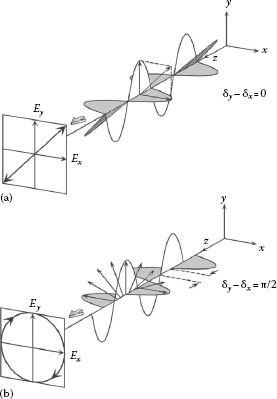
FIGURE 27.1 Representation of (a) linear polarization and (b) right-circular polarization. Phase differences between the electric fields parallel to the x- and y-axis (δy – δx) are (a) 0 and (b) π/2.
where
ω and K are the angular frequency and propagation number
E0x(E0y) and δx(δy) denote the amplitude and initial phase for the light wave oscillating in the x(y) direction
For the representation of the polarization state, relative amplitude and phase difference between Ex and Ey are important. As shown in Figure 27.1a, when δy – δx = 0, there is no phase difference between Ex and Ey, and the oscillating direction is always 45° in the x–y plane. In other words, the light wave oriented at 45° can be resolved into the two waves vibrating parallel to the x- and y-axis. When the phase difference is 90° (δy – δx = π/2), the synthesized electric filed rotates in the x–y plane as the light propagates. For δy – δx = 0 or π, the polarization state becomes linear polarization, while the polarization state is circular polarization for δy – δx = π/2 or 3π/2. These are special cases, and all the other polarization states are called elliptical polarization.
Figure 27.2 illustrates the measurement principle of ellipsometry. When light is reflected or transmitted by samples at oblique incidence, the light is classified into the p- and s-polarized light waves depending on the oscillatory direction of its electric field. In Figure 27.2, Eip(Eis) and Erp(Ers) show the incident and reflected light waves for the p-polarization (s-polarization). In p-polarization, the electric fields of Eip and Erp oscillate within the same plane, and this particular plane is called the plane of incidence. In ellipsometry measurement, the polarization states of incident and reflected light waves are defined by the coordinates of p- and s-polarization. Notice that the vectors on the incident and reflection sides overlap completely when the incident angle is θ0 = 90° (straight-through configuration). In Figure 27.2, the incident light is the linear polarization oriented at +45° relative to the Eip-axis. In particular, Eip = Eis holds for this polarization since the amplitudes of p- and s-polarization are the same and the phase difference between the polarizations is zero.
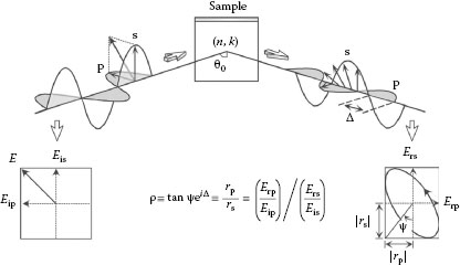
FIGURE 27.2 Measurement principle of ellipsometry.
In general, upon light reflection on a sample, p- and s-polarization shows quite different changes in amplitude and phase [1,2,7]. Ellipsometry measures the two values (ψ, Δ) that represent the relative amplitude ratio and phase difference between p- and s-polarization, respectively. In ellipsometry, therefore, the variation of light reflection with p- and s-polarization is measured as the change in a polarization state. In particular, when a sample structure is simple, the amplitude ratio ψ is characterized by the refractive index n while Δ represents light absorption described by the extinction coefficient k. In this case, the two values (n, k) can be determined directly from the two ellipsometry parameters (ψ, Δ). This is the basic principle of ellipsometry measurement.
In Figure 27.2, each wave (Eip, Eis, Erp, and Ers) is expressed by Equation 27.3. The ratio of reflected light to incident light is called the amplitude reflection coefficient r, and the ratios for the p-polarization (rp) and s-polarization (rs) are given by
Equation 27.4 represents the relative change induced by light reflection. Accordingly, upon light reflection the amplitude changes from 1 to |rp| with a relative phase change of δp for p-polarization. The (ψ, Δ) measured from ellipsometry are defined from the ratio of the amplitude reflection coefficients for p- and s-polarization:
It follows from Equation 27.4 that
As confirmed from Equation 27.4, rp and rs are originally defined by the ratios of reflected electric fields to incident electric fields and tan ψ eiΔ is defined further by the ratio of rp to rs. In the case of Figure 27.2, Equation 27.6 can be simplified to tan ψ eiΔ = Erp/Ers since Eip = Eis. By using Equations 27.4 and 27.6, we get
Thus, ψ represents the angle determined from the amplitude ratio between reflected p- and s-polarization while Δ expresses the phase difference between reflected p- and s-polarization, as shown in Figure 27.2. On the other hand, the reflectance R obtained in conventional measurements is given by
From Equation 27.8, ψ is redefined as
Accordingly, ψ represents the angle basically determined from Rp/Rs.
As confirmed from Equation 27.6, ellipsometry measures the ratio of the amplitude reflection coefficients (rp/rs). Since the difference between rp and rs is maximized at the Brewster angle [1,2,7], sensitivity for the measurement also increases at this angle. Thus, ellipsometry measurement is generally performed at the Brewster angle. The Brewster angle θB can be obtained from θB = tan−1(ns), where ns is the refractive index of samples. If ns = 3, for example, we obtain θB = 71.6°. Accordingly, the choice of the incidence angle varies according to the optical constants of samples.
Until the early 1970s, only an ellipsometry instrument called the null ellipsometry had been used for measurements [1,2]. Ellipsometry instruments that are used now can be classified into two major categories: instruments that use rotating optical elements [1,6,8,9,10,11,12,13,14,15,16,17,18,19] and instruments that use a photoelastic modulator [1,18,19,20,21,22,23,24]. The rotating-element ellipsometers can further be classified into the rotating-analyzer ellipsometry (RAE) [1,6,8,9,10,11,12,13] and rotating-compensator ellipsometry [1,14,15,16,17,18]. In this section, as the simplest ellipsometry instrument, the principle of RAE is explained in detail.
Figure 27.3 shows the schematic diagram of RAE that has been used widely up to now. This instrument consists of (light source)-polarizer-sample-(rotating analyzer)-detector. Although a polarizer and an analyzer are the same optical element, these are called separately due to the difference in their roles. Basically, the polarizer (analyzer) transmits only linearly polarized light whose direction is parallel to the transmission axis [1,4,7]. A polarizer is placed in front of a light source and is utilized to extract linearly polarized light from the unpolarized light source. On the other hand, an analyzer is placed in front of a light detector and the state of polarization is determined from the intensity of light transmitted through the analyzer. In RAE instrument, the rotation angle of the polarizer (P) is fixed (P = 45° in Figure 27.3). On the other hand, the analyzer rotates toward the direction indicated by the arrow and the rotation angle of the analyzer (A) changes continuously (A = 45° in Figure 27.3). When looking against the direction of the beam, counterclockwise rotation is the positive direction for the rotation.
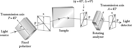
FIGURE 27.3 Schematic diagram of the measurement in RAE. In this figure, the rotation angles of the polarizer and analyzer are P = 45° and A = 45°, respectively, and the incident wave and reflected wave from a sample are linear polarizations of +45° (ψ = 45°, Δ = 0°).
Now consider that the analyzer rotates continuously with time at a speed of A = ωt, where ω is the angular frequency of the analyzer. In this case, variation of light intensity I(t) in RAE is expressed as follows [1,6,18]:
where
I0 represents the proportional constant of the reflected light whose intensity is proportional to incident light intensity
α and β are the normalized Fourier coefficients of cos 2A and sin 2A (A = ωt), respectively
It can be seen from Equation 27.10 that the light intensity varies as a function of the analyzer angle 2A. This implies that there is no distinction between the upper and lower sides of the transmission axis and the 180° rotation of the analyzer corresponds to one optical rotation.
In RAE instrument, the normalized Fourier coefficients (α, β) in Equation 27.10 are given by
Solving Equation 27.11 for (ψ, Δ) gives the following equations [1,6,19]:
Figure 27.4 shows the normalized light intensity (I0 = 1) calculated from Equation 27.10 using P = 45°, plotted as a function of the angle of the rotating analyzer A = ωt (0° ≤ A ≤ 180°). In this figure, Δ is varied from 0° to 90° with a constant value of ψ = 45°. As shown in “a” in Figure 27.4, when reflected light is linear polarization (ψ = 45°, Δ = 0°), a light intensity is maximized at A = 45° while the light intensity becomes zero at A = 135°. This result can be understood easily from an optical configuration shown in Figure 27.3. In this figure, incident light is the linear polarization of +45° (P = 45°), and the polarization state does not change upon light reflection on a sample (ψ = 45°, Δ = 0°). When A = 0°, only the p-polarized component transmits the analyzer. At A = 45°, however, the oscillatory direction of the reflected light is parallel to the transmission axis of the analyzer (Figure 27.3), and consequently the light intensity measured by the detector is maximized, as shown in “a” in Figure 27.4. When the analyzer rotates further to A = 135°, the transmission axis of the analyzer becomes perpendicular to the polarization direction of the reflected light and the light intensity becomes zero. On the other hand, when reflected light is circular polarization, the light intensity is independent of the analyzer angle, as shown in “c” in Figure 27.4. This result can be understood from the propagation of circular polarization, as shown in “b” in Figure 27.1. When reflected light is elliptical polarization, normalized light intensities are intermediate between linear and circular polarizations.
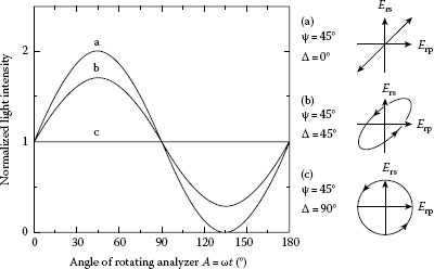
FIGURE 27.4 Normalized light intensity in the RAE, plotted as a function of the angle of rotating analyzer A = ωt. This figure summarizes the calculation results when the polarization states of reflected light are (a) ψ = 45°, Δ = 0°; (b) ψ = 45°, Δ = 45°; and (c) ψ = 45°, Δ = 90°.
From the above results, it can be seen that the shape of I(t) slides in the horizontal direction (analyzer angle) depending on a value of ψ and the amplitude of I(t) reduces as the state of polarization changes from linear to elliptical polarizations. In RAE, therefore, the polarization state of reflected light is determined from a variation of light intensity with the analyzer angle. In this method, however, right-circular polarization (δy – δx = π/2), shown in Figure 27.1b, cannot be distinguished from left-circular polarization (δy – δx = 3π/2) since these polarizations show the same light intensity variation versus the analyzer angle. Accordingly, in RAE, the measurement range for A becomes half (0° ≤ Δ ≤ 180°) [1]. If we introduce a compensator (retarder) between the sample and the analyzer in Figure 27.3, circular polarizations can be distinguished and more accurate measurement in the range of −180° ≤ Δ ≤ 180° becomes possible [1,14,15,16,17,18].
In RAE measurement, we first determine (α, β) from the Fourier analysis of measured light intensities and then extract (ψ, Δ) values by substituting the measured (α, β) into Equation 27.12.
It should be emphasized that ellipsometry allows the high-precision measurements for (ψ, Δ) because ellipsometry measures relative light intensities modulated by optical elements instead of the absolute light intensities of reflected p- and s-polarization, as shown in Figure 27.4. Accordingly, measurement errors induced by various imperfections of instruments become very small in ellipsometry measurement if we compare with absolute reflectance measurements. This is the reason why optical constants and film thickness can be estimated with high precision in ellipsometry technique.
In conventional single-wavelength ellipsometry, a He–Ne laser and photomultiplier tube are employed as a light source and detector, respectively [10]. In spectroscopic ellipsometry, the wavelength of incident light is changed using a monochromator and the monochromatic light is detected by a photomultiplier tube [6,11]. In spectroscopic ellipsometry instruments that allow real-time monitoring, white light is illuminated to a sample and all the light waves at different wavelengths are detected simultaneously using a photodiode array [13,16] or charge coupled device (CCD) detector. Up to now, the capability of spectroscopic ellipsometry measurement has been extended from the vacuum ultraviolet (VUV) region to the infrared region. For VUV ellipsometry [4,25], a deuterium lamp is used as a light source in addition to a xenon lamp used in conventional measurements in the visible/UV region. For infrared ellipsometry [1,4,5,25,26,27], Fourier-transform infrared spectrometer has been employed as a light source.
In order to evaluate the optical constants and thickness of samples from ellipsometry, data analysis using an optical model is necessary. The optical model is represented by the complex refractive index and layer thickness of each layer. Figure 27.5 shows an example of the optical model consisting of an air/thin layer/substrate structure. In this figure, N0, N1, and N2 denote the complex refractive indices of air (N0 = 1), thin layer (thickness d), and substrate, respectively. The transmission angles (θ1 and θ2) can be calculated from the angle of incidence θ0 by applying Snell’s law expressed as N0 sin θ0 = N1 sin θ1 = N2 sin θ2 [1,7]. As shown in Figure 27.5, when light absorption in a thin layer is small, optical interference occurs by multiple light reflections within the thin layer. In this case, the total amplitude reflection coefficient of the structure is given by
Here, r01 and r12 show the amplitude reflection coefficients at the air/thin layer and thin layer/substrate interfaces in Figure 27.5, respectively, and the phase thickness β is described by β = (2πdN1 cos θ1)/λ [1,7]. Note that Equation 27.13 can be applied for the calculation of both p-polarization (r012,p) and s-polarization (r012,s). From Fresnel equations, the amplitude reflection coefficients for the p-polarization (rjk,p) and s-polarization (rjk,s) at an interface jk are obtained [1,7]:
Finally, (ψ, Δ) of the structure in Figure 27.5 are calculated using Equations 27.5 and 27.13:
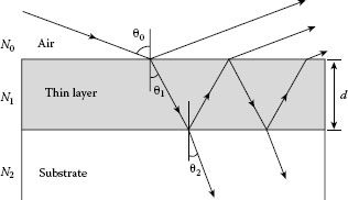
FIGURE 27.5 Optical model consisting of an air/thin layer/substrate structure.
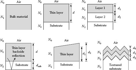
FIGURE 27.6 Optical model used in data analysis of ellipsometry.
Figure 27.6 summarizes optical models used in ellipsometry data analysis. In the optical model shown in Figure 27.6a, only the light reflection at an air/bulk material interface is taken into account, and ρ = tan ψ eiΔ of this optical model is given by ρ = rjk,p/rjk,s using Equation 27.14. When we apply this model, the thickness of the bulk material must be thick enough so that there is no light reflection from the substrate backside. In the case of this model, ε of the bulk material can be estimated directly from measured (ψ, Δ) using the following equation [1,2]:
The optical model in Figure 27.6b shows the same structure as Figure 27.5. In this optical model, the infinite thickness of a substrate is also assumed. If two thin layers are formed on a substrate (Figure 27.6c), we first calculate the amplitude reflection coefficients for layer 2 and substrate by applying Equation 27.13:
The phase variation β2 is given by β2 = (2πd2N2cos θ2)/λ, where d2 is the thickness of layer 2. From r123, we obtain the amplitude reflection coefficients for the multilayer as follows:
In Equation 27.18, β1 = (2πd1N1 cos θ1)/λ, where d1 is a thickness of layer 1. The (ψ, Δ) of this optical model can then be calculated as ρ = r0123,p/r0123,s. In this manner, the calculation can be performed upward from the substrate even if there are many layers in a multilayer structure.
As shown in Figure 27.6d, when the light absorption in a substrate is small (ε2 ~ k ~ 0) and the backside reflection of the transparent substrate is present, we need to employ an analytical model that incorporates the effect of backside reflection [1,28,29]. The thickness inhomogeneity of a thin layer also affects (ψ, Δ) spectra and this effect should be modeled appropriately [1,28,30]. So far, the analysis of a thin film formed on a textured substrate shown in Figure 27.6f has also been reported [31]. When the samples shown in Figure 27.6d through f are measured, however, polarized light used as a probe in ellipsometry is transformed into partially polarized light due to depolarization effect of the samples [1,28,29,30,31]. In such cases, measurement errors generally increase, although this effect depends completely on the type of instrument [1,16]. Thus, when we analyze samples having depolarization effects, extra care is required for the data analysis as well as the measurement itself.
Basically, ellipsometry technique is quite sensitive to surface and interface structures. Thus, it is necessary to incorporate these structures into an optical model in data analysis when such structures are present. If we apply the effective medium approximation (EMA), the complex refractive indices of surface roughness and interface layers can be calculated relatively easily [1,32]. Furthermore, from ellipsometry analysis using EMA, we can characterize each volume fraction in a composite material [33]. If the film is a two-phase composite, EMA is expressed by the following equation [1,32]:
In Equation 27.19, fa and (1 – fa) represent the volume fractions of the phases a and b whose complex dielectric constants are εa and εb, respectively. This model can be extended easily to describe a material consisting of many phases:
When a thin layer on substrates has surface roughness, the optical model in Figure 27.6c can be employed. In this case, layers 1 and 2 express surface roughness layer and thin layer, respectively. The surface roughness layer is originally composed of the layer material (N2) and air (N0 = 1). Thus, if we apply EMA for these two phases, N of surface roughness layer (N1) can be estimated relatively easily. For the calculation of N1, the volume fraction of voids (fvoid) within the surface roughness layer is required, although the analysis can also be performed assuming fvoid = 0.5 (void volume fraction is 50 vol.%). By substituting εa = N02, εb = N22, and fa = fvoid = 0.5 into Equation 27.19, ε of the surface roughness layer can be obtained. From ε, N1 is determined using . When N0 = 1, N2 = n2 = 5 (N2 = n2 – ik2, k2 = 0), and fvoid = 0.5, for example, we get N1 = n1 = 2.83. Accordingly, n1 roughly becomes half of n2 due to the presence of voids (50 vol.%) within the surface roughness layer. Notice that only N2 is required for the calculation of N1 if N0 = 1 and fvoid = 0.5 are assumed. Thus, data analysis is simplified considerably if we apply EMA. Furthermore, the complex refractive index of an interface layer can also be determined from similar calculation.
The optical constants of materials generally change depending on photon energy or wavelength of light. This optical (dielectric) response is generally referred to as the dielectric function or dielectric dispersion [1,7]. For spectroscopic ellipsometry, the dielectric function of a sample is required in the data analysis. When the dielectric function of a sample is not known, modeling of the dielectric function is necessary. Figure 27.7 illustrates the dielectric functions calculated from Lorentz model, Tauc–Lorentz model, and Drude model. It can be seen from the figure that the dielectric function shows complicated variations. When there is no light absorption in materials (k = 0), it is obvious from Equation 27.1 that ε1 = n2 and ε2 = 0. Thus, in the region of ε2 = k = 0, ε1 basically shows the contribution of n. Moreover, since ε2 = 2nk (Equation 27.1), ε2 is proportional to k. Accordingly, the ε2 peaks in Figure 27.7a and b show that light is absorbed in specific regions for photon energy or wavelength.
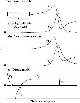
FIGURE 27.7 Dielectric functions calculated from (a) Lorentz model, (b) Tauc–Lorentz model, and (c) Drude model.
The Lorentz model in Figure 27.7a is a classical model and can be derived from a physical model assuming forced oscillation by light [1]. The expression for the Lorentz model is given by
where
En is the photon energy
A is the oscillator strength that determines the amplitude of the ε2 peak
The peak position and half width of the ε2 peak are described by En0 and Γ, respectively. In Equation 27.21, the dielectric function is expressed as the sum of different oscillators and the subscript j denotes the jth oscillator.
As shown in Figure 27.7a, in a transparent region (ε2 = k = 0), the Sellmeier or Cauchy model can be used. The Sellmeier model corresponds to a region where ε2 = 0 in the Lorentz model and this model can be derived by assuming Γ → 0 at En ≪ En0 in Equation 27.21. By using the relation ω/c = 2π/λ where c is the speed of light, the Sellmeier model is expressed by
where A and Bj represent analytical parameters used in data analysis and λ0 corresponds to En0. On the other hand, the Cauchy model is given by
The above equation can be obtained from the series expansion of Equation 27.22. Although the Cauchy model is an equation relative to the refractive index n, this is the approximate function of the Sellmeier model.
The Tauc–Lorentz model in Figure 27.7b has been employed widely to model the dielectric function of amorphous materials including a-Si [34], a-SiN:H [35], and HfO2 [36]. Recently, this model has also been applied to dielectric function modeling for transparent conductive oxides such as SnO2 [31], In2O3:Sn (ITO) [37], and ZnO [37]. As shown in Figure 27.7a, the shape of a ε2 peak calculated from the Lorentz model is completely symmetric. However, the ε2 peaks of amorphous materials generally show asymmetric shapes. In the Tauc–Lorentz model [34], therefore, ε2 is modeled from the product of a unique bandgap of amorphous materials (Tauc gap [38]) and the Lorentz model:
where
A is the amplitude
En0 is the peak position
C is the broadening parameter
Eg is the Tauc gap
Although not shown here, the equation for ε1 has also been derived using the Kramers–Kronig relations [34]. If we introduce an additional parameter ε1(∞) to express ε1 (generally ε1(∞) = 1), the Tauc–Lorentz model is described by total five parameters (ε1(∞), A, C, En0, and Eg) [34]. So far, the dielectric function of amorphous materials has also been expressed using other models including the Cody–Lorentz model [39], Forouhi–Bloomer model [40], model dielectric function (MDF) [41], and band model [42]. Furthermore, the tetrahedral model [43] and a model that extends the tetrahedral model using the EMA [44,45] have also been proposed.
On the other hand, free electrons in metals and free carriers in semiconductors absorb light and alter dielectric functions. To express the contribution of such free-carrier absorption, the Drude model has been applied widely. The Drude model is described by the following equation [1,37]:
where
ε∞ is the high-frequency dielectric constant
A is the amplitude
Γ is the broadening parameter
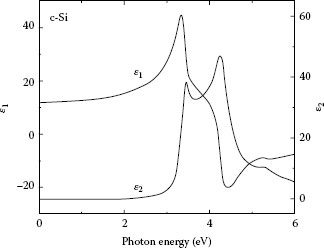
FIGURE 27.8 Dielectric function of Si crystal. (Data from Adachi, S., Optical Constants of Crystalline and Amorphous Semiconductors: Numerical Data and Graphical Information, Kluwer Academic Publishers, Norwell, MA, 1999.)
In the case of semiconductors, A can be related to carrier concentration in materials while Γ is inversely proportional to carrier mobility, and we can evaluate these values from detailed ellipsometry analysis [1,37]. When free-carrier concentration in a sample is high (typically >1018 cm−3), we can simply add the second term on the right in Equation 27.25 to other dielectric function models. In the analysis of transparent conductive oxides, dielectric function modeling has been performed ε = εTauc–Lorentz + εDrude [37].
As shown in Figure 27.7c, when the free-carrier absorption is present, the value of ε1 reduces and the free-carrier absorption described by ε2 increases rapidly at lower energies. At the energy referred to as plasma energy Ep, ε1 becomes zero and ε1 shows negative values at En < Ep. When ε1 < 0, the electric field of the incident light is screened by the free carriers present at a material surface. Consequently, the electric field of the light cannot penetrate into the material and the light reflection becomes quite strong.
Figure 27.8 shows the dielectric function of Si crystal (c-Si) [46]. As confirmed from this figure, actual dielectric functions show rather complicated structures. Since the bandgap Eg of c-Si is 1.1 eV, ε2 = k = 0 at En < 1.1 eV. In this region, the optical constant shows constant values of ε1 = n2 = 11.6 (n = 3.41). In Figure 27.8, there are two sharp ε2 peaks at 3.4 and 4.25 eV that represent optical transitions at Λ and X points in the c-Si band structure [47]. If we perform the analysis using a transparent region of En < 2.5 eV (ε2 ~ k ~ 0), we can model the dielectric function of c-Si rather easily [48]. So far, in order to express the dielectric functions of semiconductors, various models including the Lorentz model, harmonic oscillator approximation (HOA) [49], band model [42], MDF [41,50], and parametric semiconductor model [51] have been developed.
For simple ellipsometry characterization, ellipsometry measurement at a single wavelength using a He–Ne layer (λ = 632.8 nm) has been performed widely [10]. When a thin SiO2 layer formed on c-Si is evaluated, the single wavelength ellipsometry has commonly been used [10,52]. For the structure, the optical model shown in Figure 27.6b can be employed assuming no surface roughness and interface layers. In this case, (ψ, Δ) are calculated from Equation 27.15 and the parameters used in the calculation are described as
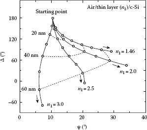
FIGURE 27.9 ψ – Δ trajectory in an air/thin layer/c-Si structure. In this calculation, θ0 = 70°, and the refractive index of the thin layer (N1 = n1) was changed from 1.46 to 3.0. Open circles show the values at every 10 nm.
Since values of N2 and θ0 are usually known and N0 = 1, there are total three unknown parameters in Equation 27.26: (n1, k1) of N1 = n1 – ik1 and d. If a thin layer does not show any light absorption at the measured wavelength (k1 = 0), the unknown parameters become only n1 and d. In this case, (n1, d) of the layer can be estimated directly from two measured values (ψ, Δ) obtained by a single wavelength measurement.
Figure 27.9 shows the ψ – Δ trajectory when the refractive index of a thin transparent layer (N1 = n1) on a c-Si substrate is varied from 1.46 (SiO2 to 3.0 in the calculation of Equation 27.15. For the calculation, θ0 = 70°, N0 = 1, and N2 = 3.87 – i0.0146 [53] (c-Si substrate at λ = 632.8 nm) were used. The open circles in Figure 27.9 represent the values at every nm, and the (ψ, Δ) values move toward the direction of arrows with increasing layer thickness. It can be seen from Figure 27.9 that the (ψ, Δ) values change largely according to the (n1, d) values and, from measured (ψ, Δ) values, (n1, d) of a thin layer can be evaluated analytically. In Figure 27.9, however, ψ is almost constant in the region of d < 10 nm, although Δ shows large changes. This arises from the fact that Rp and Rs show almost no changes at d < 10 nm, even when n1 is varied in the wide range. Recall from Equation 27.9 that ψ = tan−1[(Rp/Rs)1/2]. Consequently, the evaluation of n1 becomes difficult when the thickness of a transparent layer is quite thin (d < 10 nm), although d can still be estimated if n1 is known. Thus, when thin layers are characterized, we determine d using n1 obtained from the analysis of thick layers.
In contrast to single-wavelength ellipsometry, (ψ, Δ) spectra are measured in spectroscopic ellipsometry. From the analysis of these spectra, various characterizations including bandgap and phase structures become possible [1]. Furthermore, even when a thin layer on substrates shows light absorption (k > 0) or samples have complicated layer structures, ellipsometry analyses can be performed [1]. Figure 27.10 shows a simple example of spectroscopic ellipsometry analysis. The sample is a SiO2 thermal oxide formed on a c-Si substrate. The optical model of this sample also corresponds to the one shown in Figure 27.6b. Here, we use θ0 = 75°, N0 = 1, and the reported value for N2 [53]. Thus, the analysis parameters are only (n1, d) as described earlier. Since SiO2 is a transparent material, the Sellmeier or Cauchy model can be applied to the analysis. As shown in Equation 27.23, the Cauchy model is expressed by the three parameters (A, B, C). Accordingly, when the Cauchy model is applied to calculate N1(n1), the final analysis parameters in the air/SiO2/c-Si structure become (A, B, C, d).
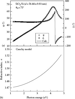
FIGURE 27.10 (a) (ψ, Δ) spectra obtained from a SiO2/c-Si substrate structure and (b) refractive index spectrum of the SiO2 layer deduced from the Cauchy model. In (a), the incidence angle of the measurement is θ0 = 75°.
Figure 27.10a shows the (ψ, Δ) spectra of a sample having the SiO2/c-Si structure. The solid lines in the figure show the calculated spectra obtained from the fitting analysis. From the analysis, A = 1.469, B = 2.404 × 10⁻³ μm2, C = 7.357 × 10⁻⁵ μm4, and d = 56.44 ± 0.03 nm are estimated. Figure 27.10b shows the refractive index spectrum of the SiO2 layer calculated from these (A, B, C) values. In spectroscopic ellipsometry, the construction of an optical model and modeling of dielectric function are performed in this manner, and from the fitting analysis, the optical constants and thickness of a sample are evaluated. In particular, since the measurement of spectroscopic ellipsometry is performed in a wide wavelength region, even if there are several analysis parameters, these values can be estimated from the analysis. Accordingly, more reliable analysis can be performed from (ψ, Δ) spectra measured in a wider wavelength region with a larger number of data points. This example shows clearly that we can determine film thickness very precisely from spectroscopic ellipsometry. It has been reported that SiO2 thicknesses estimated from ellipsometry show excellent agreement with those characterized by transmission electron microscope [54], x-ray photoemission spectroscopy [55], and capacitance-voltage measurements [55].
When we characterize the refractive index spectrum and thickness of SiO2 layers, the above analysis is generally sufficient. If we employ the reported dielectric function for SiO2 [53], d is determined more easily. The fitting in the analysis can be improved by increasing the number of parameters in the Cauchy or Sellmeier model. Nevertheless, for the accurate characterization of SiO2 layers, it is necessary to take the influence of an interface layer into account. In particular, it has been confirmed that the overall refractive index of SiO2 layers decreases with increasing d [53,54]. This implies that there exists the interface layer with high refractive index at the SiO2/c-Si interface [53,54,56], In other words, the effect of the interface layer becomes insignificant as d increases since the high refractive index of the interface layer is averaged out by thicker bulk layers. The presence of the interface layer has been attributed to the formation of suboxide (SiOx [x < 2]) at the SiO2/c-Si interface [56]. Thus, for accurate characterization of the SiO2 layer, the optical model consisting of air/SiO2 layer/interface layer/substrate has been employed [53,56],
As we have seen in the above example, when the dielectric function of a sample is not known, dielectric function modeling is required. Nevertheless, complete modeling of the dielectric function in a wide wavelength range is often difficult. In this case, if we use a method known as mathematical inversion, the dielectric function in a whole measured range can be extracted rather easily. F s example, the optical model of a sample is given by an air/thin layer/substrate structure. If known parameters are assumed to be measured (ψ, Δ), N0, N2, and θ0, unknown parameters become N1 and d. Now suppose that the dielectric function of the thin layer changes smoothly in a region f t model using the parameters (A, B, C). In this case, the fitting at En = a ~ b can be performed easi d sis, now the unknown parameter becomes only N1 = n1 – ik1. Thus, if we solve Equation 27.26, the measured (ψ, Δ) can be converted directly into (n1, k1) (Figure 27.11c). This procedure is referred to as the mathematical inversion. Actual mathematical inversion, however, is performed for each wavelength using linear regression analysis. Thus, the mathematical inversion is also called the optical constant fit or point-by-point fit. As shown in Figure 27.11c, from mathematical inversion, the optical constants in the whole measured range can be determined. This data analysis procedure is quite effective in determining the dielectric function of a sample, particularly when dielectric function modeling is difficult in some specific regions.
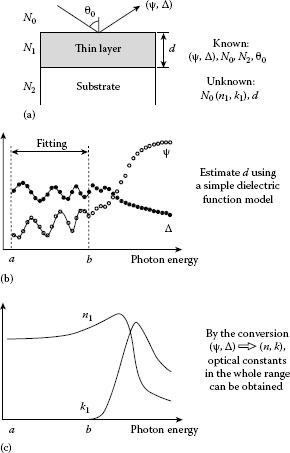
FIGURE 27.11 Schematic diagram of ellipsometry data analysis using mathematical inversion: (a) optical model, (b) fitting in selected region, and (c) optical constants of thin film.
Figure 27.12 shows an example of the ellipsometry analysis using mathematical inversion. Here, the sample is a ZnO:Ga thin layer formed on a substrate. The substrate is c-Si covered with SiO2 (50 nm), and the analysis of this substrate can be performed by the same procedure shown in Figure 27.10. If we assume that the ZnO:Ga layer has surface roughness, the optical model of this sample is expressed by the two layer model shown in Figure 27.6c, that is, air/layer 1 (surface roughness layer)/layer 2 (ZnO:Ga layer)/substrate (SiO2/c-Si) structure. If we calculate N1 (surface roughness layer) from N2 (ZnO:Ga layer) by applying EMA (fvoid = 0.5) using Equation 27.19 and determine the SiO2 layer thickness (dSiO ~ 50 nm) prior to the ZnO:Ga formation, the unknown parameters of this optical model become (N2, d1, d2). Although the ZnO layer is doped with Ga, the effect of free-carrier absorption in this layer is negligible, and we employ the Tauc–Lorentz model to represent the dielectric function of the ZnO:Ga layer. The free parameters in the Tauc–Lorentz model are (A, C, En0, Eg) if we assume ε1(∞) = 1. Accordingly, the final analysis parameters of this sample are (A, C, En0, Eg, d1, d2).
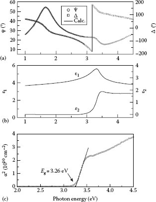
FIGURE 27.12 (a) (ψ, Δ) spectra obtained from a ZnO:Ga/SiO2/c-Si substrate structure, (b) dielectric function of the ZnO:Ga layer, and (c) α2 obtained from the ZnO:Ga dielectric function in (b). The bandgap is estimated from the intercept at α2 = 0.
Figure 27.12a shows the (ψ, Δ) spectra obtained from the sample. The ellipsometry measurement of this sample was carried out at θ0 = 70°. In this figure, the peak position of ψ represents the ZnO:Ga layer thickness and shifts toward lower energies with increasing layer thickness. The solid lines show the fitting result obtained from the calculation. In this analysis, however, the analyzed energy region is limited at En < 3.0 eV in order to avoid the complicated structures observed in the dielectric function of ZnO:Ga. From this analysis, the thickness parameters can be estimated (d1 = 3.5 ± 0.1 nm and d2 = 57.8 ± 0.1 nm). In this case, we can perform the mathematical inversion to extract the dielectric function of ZnO:Ga in the whole measured region. Figure 27.12b shows the dielectric function of the ZnO:Ga layer extracted from the mathematical inversion. At lower energies (En < 3.0 eV), however, the dielectric function calculated from the Tauc–Lorentz model is shown to eliminate spectral noise. It can be confirmed from Figure 27.12a and b that only the transparent region (ε2 ~ 0) in ZnO:Ga has been used in the analysis to estimate d1 and d2. As shown by this example, the mathematical inversion is quite effective in determining dielectric functions of unknown layers.
Since ZnO is a direct bandgap material [57], the absorption coefficient can be approximated by α = A(En – Eg)1/2 [1]. Thus, the bandgap Eg of ZnO is estimated by plotting α2 versus En. Figure 27.12c shows α2 versus En for the ZnO:Ga. The absorption coefficient can be obtained easily from the dielectric function using Equations 27.1 and 27.2. The solid line shows the linear fit to the experimental data, and Eg is estimated from the intercept at α2 = 0 (Eg = 3.26 eV).
From spectroscopic ellipsometry, various information including optical constants (properties) and thickness parameters can be obtained. From the analysis of free-carrier absorption, we can even evaluate electrical properties accurately [37]. As mentioned earlier, however, ellipsometry is an indirect characterization technique, and the analysis is performed using an optical model. It should be emphasized that an optical model used in ellipsometry analysis merely represents an approximated sample structure, and obtained results are not necessarily correct even when the fitting is sufficiently good. Accordingly, when the optical constants or layer structures of a sample are not well known, we must justify ellipsometry results using other measurement methods. This is the greatest disadvantage of ellipsometry technique. However, once an analytical method is established, it becomes possible to perform various high-precision characterizations in a short time using ellipsometry.
1. H. Fujiwara, Spectroscopic Ellipsometry: Principles and Applications, Wiley, West Sussex, U.K., 2007.
2. R. M. A. Azzam and N. M. Bashara, Ellipsometry and Polarized Light, North-Holland, Amsterdam, the Netherlands, 1977.
3. H. G. Tompkins and W. A. McGahan, Spectroscopic Ellipsometry and Reflectometry: A User’s Guide, John Wiley & Sons, New York, 1999.
4. H. G. Tompkins and E. A. Irene (eds.), Handbook of Ellipsometry, William Andrew, New York, 2005.
5. M. Schubert, Infrared Ellipsometry on Semiconductor Layer Structures: Phonons, Plasmons, and Polaritons, Springer, Heidelberg, Germany, 2004.
6. R. W. Collins, Automatic rotating element ellipsometers: Calibration, operation, and real-time applications, Rev. Sci. Instrum. 61: 2029–2062, 1990.
7. E. Hecht, Optics, 4th edn., Addison Wesley, San Francisco, CA, 2002.
8. W. Budde, Photoelectric analysis of polarized light, Appl. Opt. 1: 201–205, 1962.
9. B. D. Cahan and R. F. Spanier, A high speed precision automatic ellipsometer, Surf. Sci. 16: 166–176, 1969.
10. P. S. Hauge and F. H. Dill, Design and operation of ETA, an automated ellipsometer, IBM J. Res. Dev. 17: 472–489, 1973.
11. D. E. Aspnes and A. A. Studna, High precision scanning ellipsometer, Appl. Opt. 14: 220–228, 1975.
12. R. H. Muller, Present status of automatic ellipsometers, Surf. Sci. 56: 19–36, 1976.
13. I. An, Y. M. Li, H. V. Nguyen, and R. W. Collins, Spectroscopic ellipsometry on the millisecond time scale for real-time investigations of thin-film and surface phenomena, Rev. Sci. Instrum. 63: 3842–3848, 1992.
14. P. S. Hauge and F. H. Dill, A rotating-compensator Fourier ellipsometer, Opt. Commun. 14: 431–437, 1975.
15. P. S. Hauge, Generalized rotating-compensator ellipsometry, Surf. Sci. 56: 148–160, 1976.
16. J. Lee, P. I. Rovira, I. An, and R. W. Collins, Rotating-compensator multichannel ellipsometry: Applications for real time Stokes vector spectroscopy of thin film growth, Rev. Sci. Instrum. 69: 1800–1810, 1998.
17. R. W. Collins, J. Koh, H. Fujiwara, P. I. Rovira, A. S. Ferlauto, J. A. Zapien, C. R. Wronski, and R. Messier, Recent progress in thin film growth analysis by multichannel spectroscopic ellipsometry, Appl. Surf. Sci. 154–155: 217–228, 2000.
18. P. S. Hauge, Recent developments in instrumentation in ellipsometry, Surf. Sci. 96: 108–140, 1980.
19. D. E. Aspnes, Spectroscopic ellipsometry of solids, in Optical Properties of Solids: New Developments, B. O. Seraphin (ed.), Chapter 15, pp. 801–846, North-Holland, Amsterdam, the Netherlands, 1976.
20. S. N. Jasperson and S. E. Schnatterly, An improved method for high reflectivity ellipsometry based on a new polarization modulation technique, Rev. Sci. Instrum. 40: 761–767, 1969.
21. S. N. Jasperson, D. K. Burge, and R. C. O’Handley, A modulated ellipsometer for studying thin film optical properties and surface dynamics, Surf. Sci. 37: 548–558, 1973.
22. B. Drévillon, J. Perrin, R. Marbot, A. Violet, and J. L. Dalby, Fast polarization modulated ellipsometer using a microprocessor system for digital Fourier analysis, Rev. Sci. Instrum. 53: 969–977, 1982.
23. O. Acher, E. Bigan, and B. Drévillon, Improvements of phase-modulated ellipsometry, Rev. Sci. Instrum. 60: 65–77, 1989.
24. W. M. Duncan and S. A. Henck, In situ spectral ellipsometry for real-time measurement and control, Appl. Surf. Sci. 63: 9–16, 1993.
25. J. N. Hilfiker, C. L. Bungay, R. A. Synowicki, T. E. Tiwald, C. M. Herzinger, B. Johs, G. K. Pribil, and J. A. Woollam, Progress in spectroscopic ellipsometry: Applications from vacuum ultraviolet to infrared, J. Vac. Sci. Technol. A 21: 1103–1108, 2003.
26. A. Röseler, IR spectroscopic ellipsometry: Instrumentation and results, Thin Solid Films 234: 307–313, 1993.
27. A. Canellas, E. Pascual, and B. Drévillon, Phase-modulated ellipsometer using a Fourier transform infrared spectrometer for real time applications, Rev. Sci. Instrum. 64: 2153–2159, 1993.
28. J.-Th. Zettler, Th. Trepk, L. Spanos, Y.-Z. Hu, and W. Richter, High precision UV-visible-near-IR Stokes vector spectroscopy, Thin Solid Films 234: 402–407, 1993.
29. R. Joerger, K. Forcht, A. Gombert, M. Köhl, and W. Graf, Influence of incoherent superposition of light on ellipsometric coefficients, Appl. Opt. 36: 319–327, 1997.
30. G. E. Jellison, Jr. and J. W. McCamy, Sample depolarization effects from thin films of ZnS on GaAs as measured by spectroscopic ellipsometry, Appl. Phys. Lett. 61: 512–514, 1992.
31. P. I. Rovira and R. W. Collins, Analysis of specular and textured SnO2:F films by high speed four-parameter Stokes vector spectroscopy, J. Appl. Phys. 85: 2015–2025, 1999.
32. D. E. Aspnes, Optical properties of thin films, Thin Solid Films 89: 249–262, 1982.
33. M. Wakagi, H. Fujiwara, and R. W. Collins, Real time spectroscopic ellipsometry for characterization of the crystallization of amorphous silicon by thermal annealing, Thin Solid Films 313–314: 464–468, 1998.
34. G. E. Jellison, Jr. and F. A. Modine, Parameterization of the optical functions of amorphous materials in the interband region, Appl. Phys. Lett. 69: 371–373, 1996; Erratum, Appl. Phys. Lett. 69: 2137, 1996.
35. G. E. Jellison, Jr., F. A. Modine, P. Doshi, and A. Rohatgi, Spectroscopic ellipsometry characterization of thin-film silicon nitride, Thin Solid Films 313–314: 193–197, 1998.
36. Y. J. Cho, N. V. Nguyen, C. A. Richter, J. R. Ehrstein, B. H. Lee, and J. C. Lee, Spectroscopic ellipsometry characterization of high-k dielectric HfO2 thin films and the high-temperature annealing effects on their optical properties, Appl. Phys. Lett. 80: 1249–1251, 2002.
37. H. Fujiwara and M. Kondo, Effects of carrier concentration on the dielectric function of ZnO:Ga and In2O3:Sn studied by spectroscopic ellipsometry: Analysis of free-carrier and band-edge absorption, Phys. Rev. B 71: 075109, 2005.
38. J. Tauc, R. Grigorovici, and A. Vancu, Optical properties and electronic structure of amorphous germanium, Phys. Stat. Sol. 15: 627–637, 1966.
39. A. S. Ferlauto, G. M. Ferreira, J. M. Pearce, C. R. Wronski, R. W. Collins, X. Deng, and G. Ganguly, Analytical model for the optical functions of amorphous semiconductors from the near-infrared to ultraviolet: Applications in thin film photovoltaics, J. Appl. Phys. 92: 2424–2436, 2002.
40. A. R. Forouhi and I. Bloomer, Optical dispersion relations for amorphous semiconductors and amorphous dielectrics, Phys. Rev. B 34: 7018–7026, 1986.
41. S. Adachi, Optical Properties of Crystalline and Amorphous Semiconductors: Materials and Fundamental Principles, Kluwer Academic Publishers, Norwell, MA, 1999.
42. J. Leng, J. Opsal, H. Chu, M. Senko, and D. E. Aspnes, Analytic representations of the dielectric functions of crystalline and amorphous Si and crystalline Ge for very large scale integrated device and structural modeling, J. Vac. Sci. Technol. A 16: 1654–1657, 1998.
43. H. R. Philipp, Optical properties of non-crystalline Si, SiO, SiOx and SiO2, J. Phys. Chem. Solids 32: 1935–1945, 1971.
44. D. E. Aspnes and J. B. Theeten, Dielectric function of Si-SiO2 and Si-Si3N4 mixtures, J. Appl. Phys. 50: 4928–4935, 1979.
45. K. Mui and F. W. Smith, Optical dielectric function of hydrogenated amorphous silicon: Tetrahedron model and experimental results, Phys. Rev. B 38: 10623–10632, 1988.
46. S. Adachi, Optical Constants of Crystalline and Amorphous Semiconductors: Numerical Data and Graphical Information, Kluwer Academic Publishers, Norwell, MA, 1999.
47. U. Schmid, N. E. Christensen, and M. Cardona, Relativistic band structure of Si, Ge, and GeSi: Inversion-asymmetry effects, Phys. Rev. B 41: 5919–5930, 1990.
48. G. E. Jellison, Jr. and F. A. Modine, Optical functions of silicon at elevated temperatures, J. Appl. Phys. 76: 3758–3761, 1994.
49. M. Erman, J. B. Theeten, P. Chambon, S. M. Kelso, and D. E. Aspnes, Optical properties and damage analysis of GaAs single crystals partly amorphized by ion implantation, J. Appl. Phys. 56: 2664–2671, 1984.
50. T. Suzuki and S. Adachi, Optical properties of amorphous Si partially crystallized by thermal annealing, Jpn. J. Appl. Phys. 32: 4900–4906, 1993.
51. B. Johs, C. M. Herzinger, J. H. Dinan, A. Cornfeld, and J. D. Benson, Development of a parametric optical constant model for Hg1-xCdxTe for control of composition by spectroscopic ellipsometry during MBE growth, Thin Solid Films 313–314: 137–142, 1998.
52. E. A. Irene, Application of spectroscopic ellipsometry to microelectronics, Thin Solid Films 233: 96–111, 1993.
53. C. M. Herzinger, B. Johs, W. A. McGahan, J. A. Woollam, and W. Paulson, Ellipsometric determination of optical constants for silicon and thermally grown silicon dioxide via a multi-sample, multi-wavelength, multi-angle investigation, J. Appl. Phys. 83: 3323–3336, 1998.
54. A. Kalnitsky, S. P. Tay, J. P. Ellul, S. Chongsawangvirod, J. W. Andrews, and E. A. Irene, Measurements and modeling of thin silicon dioxide films on silicon, J. Electrochem. Soc. 137: 234–238, 1990.
55. M. L. Green, E. P. Gusev, R. Degraeve, and E. L. Garfunkel, Ultrathin (<4 nm) SiO2 and Si–O–N gate dielectric layers for silicon microelectronics: Understanding the processing, structure, and physical and electrical limits, J. Appl. Phys. 90: 2057–2121, 2001.
56. D. E. Aspnes and J. B. Theeten, Optical properties of the interface between Si and its thermally grown oxide, Phys. Rev. Lett. 43: 1046–1050, 1979.
57. Y. Mi, H. Odaka, and S. Iwata, Electronic structures and optical properties of ZnO, SnO2 and In2O3, Jpn. J. Appl. Phys. 38: 3453–3458, 1999.