
CONTENTS
31.1.3 Interference Microscopy
31.2.1 Interference Signals and Patterns
31.2.2 Phase Shifting Interferometry
31.2.3 Coherence Scanning Interferometry
31.3 Instrument Design for Interference Microscopy
31.3.1 Light Source and Detection
31.4.1 Modeling of Interference Microscopy Fringe Patterns
31.5.1 Good Practice and Instrument Evaluation
31.5.2 Surface Topography Repeatability
31.5.3 Vibration and Environmental Effects
31.5.4 Optical Effect of Surface Materials
31.5.6 Field of View and Slope Acceptance
This chapter considers the principles of interferometric dimensional metrology applied to surface features best viewed in a microscope. Interference microscopy encompasses a wide variety of techniques for measuring surface texture, shape, step heights, lateral positions and dimensions, transparent film structure, and the scattering behavior of optically unresolved patterns. In addition to applications that range from semiconductor wafer analysis to fuel injection valve measurements, interference microscopy encompasses a variety of basic geometries from Mirau to Michelson and light sources from lasers to light-emitting diodes (LEDs). As with companion techniques such as confocal microscopy, interference microscopy enjoys the advantages of rapid, noncontact operation and rapid data acquisition, often at data acquisition rates in the millions of 3D image points per second. Unique among optical areal measurements instruments, interferometry has the benefit of high sensitivity to surface structure irrespective of magnification.
The physical concepts and fundamental instrument geometries underlying interference microscopy have a history reaching back to the nineteenth century, but the more recent developments of the technique link closely to rapidly advancing enabling technologies, particularly in digital data processing. While the modern age of interferometry for testing of optical components was born with the helium–neon laser, automated interference microscopy owes its existence to the desktop computer. The differences relate to the relative complexity of the interference signals generated in the high-magnification optical systems required to see small features and to the kinds of surface structures that interest us in microscopy. These factors modify the interference patterns with effects related to focus position, incoherent imaging, discrete surface structure, roughness, and semi-transparent films. Making good use of the resulting interference patterns requires sophisticated data acquisition and analysis commanded by a computer.
The modern age of interference microscopy began therefore in the 1980s, initially with singlepoint systems [1], then with single-line optical profilers based on phase shifting interferometry (PSI) [2,3]. Full-field areal topography imaging using computerized phase shifting completed the basic functions of automated 3D imaging on the microscopic scale [4], but applications remained limited, primarily by the requirement that the surface be optically smooth, so as to generate clear, continuous interference patterns across the surface with a light source filtered to a narrow spectral bandwidth. This limitation fell away with the discovery that meaningful topographical imaging was possible even when the interference image was a seemingly indecipherable speckle pattern, using the full spectral bandwidth of white light illumination [5] and a technique known as white light or coherence scanning interferometry (CSI) [6]. Coherence scanning is now the dominant method for interferometric 3D surface structure analysis on the microscopic scale, with expanding commercial offerings and tens of thousands of instruments installed worldwide. Modern systems have overcome previous limitations of environmental robustness, slope acceptance, profile fidelity, and correlation to other surface topography methods.
31.1.3 INTERFERENCE MICROSCOPY
The most common form of interference microscope today for areal surface structure requires that the object be in focus and operates by comparing the sample surface to a physical or virtual reference surface by two-beam division of amplitude interferometry. The schematic geometry of Figure 31.1 fits this description. The overall structure is that of a common microscope with a digital camera, but equipped with a specialized interference objective, which in most cases is mechanically and optically interchangeable with a conventional noninterferometric imaging objective. Figure 31.2 illustrates a typical interference fringe pattern for a roughness specimen, while Figure 31.3 shows the resulting topography image generated by automated modulation of the fringe pattern followed by detailed computer analysis. Figure 31.2 illustrates how interference fringes follow the surface contours, as well as the effects of limited coherence that modulate the fringe contrast—an important characteristic of modern coherence scanning methods. This chapter concentrates on reflectionmode surface measuring interferometers of this general type.
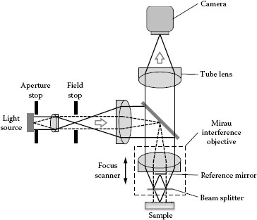
FIGURE 31.1 Interference microscope for areal surface structure analysis.
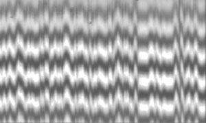
FIGURE 31.2 Fringe pattern for a reflection interference microscope as in Figure 31.1, showing interference fringes that follow the surface height contours a roughness specimen.
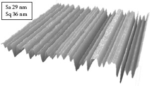
FIGURE 31.3 Surface topography measurement corresponding to Figure 31.2.
31.2.1 INTERFERENCE SIGNALS AND PATTERNS
The simplified Michelson interferometer illustrated in Figure 31.4 with a laser source provides a foundation for understanding the basics of interferometric surface topography measurement. Following the usual two-beam interference analysis, the interference signal at the square-law detector can be written [7,8] as
where IDC and IAC are fixed coefficients. The small inset graph in Figure 31.4 shows the sinusoidally modulated intensity as a function of the difference (h – ζ). The fringe frequency
is the rate at which the interference signal oscillates as a function of changes in sample surface height h or in position ζ of the reference mirror. This frequency depends on the wavelength λ but, as we shall see later, geometric factors as well when we consider the more complex and interesting geometries of interference microscopes. The phase offset γ relates among other factors to the reflection and transmission properties of the interferometer components.
In a surface topography measurement, a camera replaces the detector in Figure 31.4 and associated imaging optics bring the sample surface into focus, allowing for intensity values to correspondto specific points on the surface. In surface structure analysis, most often we are interested in the height h, which we extract by inversion of the detected phase
that appears inside the argument of the cosine in Equation 31.1. For the special case where all factors in Equation 31.1 are constant with the exception of surface height, then there are straightforward ways to infer the relative phase θ as it varies across a surface by inspection of the intensity value I. In Figure 31.2, the interference fringes, corresponding to lines of equal intensity, follow the surface topography as contours of equal surface height h. In the earliest applications of interference microscopy, skilled observers would estimate surface texture to a small fraction of a micron based on the appearance of these fringes, first with the aid of reticles and later by means of photometric tools.
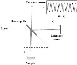
FIGURE 31.4 Conceptual diagram of a Michelson interferometer.
31.2.2 PHASE SHIFTING INTERFEROMETRY
Increased precision and greater surface structure complexity require something more automated than visual inspection of lines of equal interference intensity. Electronic data acquisition together with computerized data analysis allows for quantification of surface texture at the nanometer level, over surfaces that may have highly variable reflectivity and structure. With the exception of carrier fringe analyses similar to holographic methods [9], computerized fringe analysis almost invariably relies on digitization of image data acquired during a controlled phase shift, most often over time, and introduced by controlled mechanical oscillation of an interference objective in the focus direction indicated in Figure 31.1.
The earliest and still one of the most precise and widespread computerized fringe analysis methods is PSI. Here, the extraction of this phase involves heterodyning the signal by means of a controlled phase shift φ, for example, by modulation of the reference length ζ:
where φ = ζK and the constant phase offset γ has been dropped as unimportant here. In practice, these phase shifts correspond to a sequence of discrete sample intensities
Given that the constants IDC, IAC are typically unknown a priori, we need at least three values for φ to solve for θ.
In the most common case, these discrete phase shifts φj are evenly spaced by a phase increment α
as illustrated in Figure 31.5 for three data samples indexed j = 1, 2, 3. These data points represent either instantaneous acquisitions or phase steps, or more commonly, the center points for intensity measurements integrated over the period of time between sample points, in a method commonly referred to as the integrating bucket method [10,11].
Once we have these samples over at least one full fringe cycle, a phase detection or PSI algorithm provides the phase θ. A simple and historically significant example of such an algorithm uses just three samples [12]:
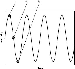
FIGURE 31.5 Intensity sampling for PSI with a linear phase shift (constant phase step between acquisitions).
where the phase shift between data acquisitions is α = 2π/3. Improving camera and data processing technologies together with increased demands on performance have driven the number of data samples and corresponding phase shifts to larger numbers, and it is now common to encounter PSI algorithms of a dozen or more sample points with floating-point coefficients. The methodology of PSI algorithm design is perhaps the single most thoroughly analyzed feature of modern computerized interferometry for surface measurements [13,14,15] and has been extensively reviewed, for example, in the excellent book chapter by Schreiber and Bruning [16].
The phase shifts ϕ need not necessarily be evenly spaced to be useful for PSI. An alternative for continuous data acquisition and averaging is sinusoidal phase shifting, a technique that has the advantage of being less demanding on phase shift mechanisms than repeated linear ramps [17]. This can be especially interesting for interference microscopes, where the phase shifting mechanism may be a compliant structure with a collection of turret-selectable objectives [18]. The intensity pattern resulting from a sinusoidal phase shift is a superposition of multiple harmonics of the original phase modulation. Although the signal as shown in Figure 31.6 is very different from a linear phase shift, the appearance of sinusoidal phase shift algorithms is similar, involving the arctangent of a ratio of weighted sums, as in the following 12-sample algorithm [19,20]:
where
for j = 1, 2, …, 6.
The evaluation of phase θ = hK using PSI involves the inverse of an arctangent function, which has a domain of −π < θ ≤ π or a height range of 2π/K, which for a simple low-NA interferometer such as in Figure 31.4 corresponds to one-half the wavelength of light. Given that the vast majority of sample surfaces require a larger metrology range, if for no other reason than to accommodate part positioning, it is standard practice to augment this range by a process known as phase connecting or unwrapping. The basic premise is that at least locally there is continuity in the surface structure to within the 2π/K limit, allowing for integration of the phase changes across the surface. This allows for removal of what is commonly referred to as the fringe-order ambiguity, where fringe order refers to an integer multiple of the 2π unambiguous range of the interference phase. One of the most common failure modes for interferometers is a mistaken fringe order, resulting in false steps or sharp features in the topography data. Techniques for unwrapping fringes robustly have been extensively studied in view of the desire to accommodate difficult surface structures and noisy interference patterns [21] (Figure 31.7).
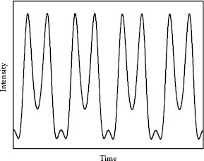
FIGURE 31.6 Example intensity pattern for PSI with a sinusoidal phase shift. The shape of such patterns varies with phase and with the amplitude of the sinusoidal phase shift function.
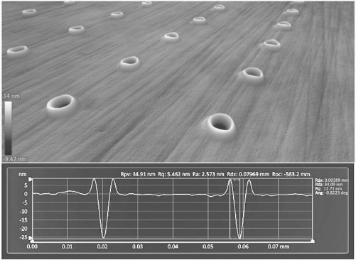
FIGURE 31.7 Example 3D PSI image of a laser textured disk.
31.2.3 COHERENCE SCANNING INTERFEROMETRY
For surface structures that have discrete features larger than the 2π limit, the issue of fringe order ambiguity becomes a fundamental limitation for many traditional interferometric methods of surface structure analysis. The canonical example is a step height feature illustrated in Figure 31.8a. Because of the lack of continuity in the interference fringes, the relative fringe order is uncertain without some approximate prior knowledge (within a half wavelength) of the step height value. For generations, the solutions have been either to employ multiple wavelengths and variations of the method of excess fractions, as in gage block interferometry [22], or to employ white light or low coherence interferometry [23]. In visual interference microscopes, prior to the era of computerized data analysis, white light fringes appear colored to the eye because of the wavelength dependence of the interference fringe periodicity. Skilled observers were able to infer step heights well beyond the 2π limit by observation of these fringes, referring to interference color charts as a guide. In black and white digital cameras, the effect reduces to one of fringe contrast; but this is still effective over a limited range, as is clear from Figure 31.8b. From the white light interferometry image, it is possible to establish visually that the step height in Figure 31.8 is about midway between 6 and 7 fringes tall, which for a 570 nm wavelength and taking into account the double-pass on reflection is 1.85 μm; not far from the calibrated value of 1.80 μm.
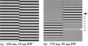
FIGURE 31.8 Tilt fringes on a 1.80 μm step height viewed with narrow spectral bandwidth illumination (a) and with white light illumination (b).
As interference microscopes became automated, it was natural to consider first using multiple wavelengths [24,25,26] and then the contrast modulation of interferometry in white light [27,28,29] to increase measurement range. The significance of this evolution was not fully realized until the early 1990s when it was found that computer analysis of white light fringes could be effective on surfaces that are so rough that continuous interference fringes in the traditional sense are no longer discernible anywhere in the image because of surface texture [5,30].
CSI, which encompasses white light interferometry, generally refers to any method for which the localization of interference fringes during a scan of optical path length provides a means to determine a surface topography map [6,31,32]. Figure 31.9 shows a typical CSI signal, illustrating the term localization by means of a calculated fringe-contrast modulation envelope. The fringe localization follows from the mutual coherence of the two interfering wavefronts. For white light fringes at low magnifications, the position of peak coherence is near the position of zero group-velocity optical path difference (OPD)—also known as the stationary phase point [33]. More generally, the fringe localization is the result of a combination of spectral and geometric factors that limit both the temporal and spatial coherence [34]. The dominant geometric effects are associated with the numerical aperture (NA) of the objective, defined in Figure 31.10.
Over a full imaging field on a smooth object, the localization of fringe contrast creates a compelling visual concept for the measurement principle. As shown in Figure 31.11, CSI relies on identifying surface heights by the mere presence of interference fringes during a mechanical scan of the interference objective shown in Figure 31.2. For those familiar with confocal microscopy, the peak fringe contrast is analogous to the position of best focus and the concept of 3D sectioning by scanning the objective. At NA values characteristic of high magnification, the position of peak fringe contrast is indeed quite close to the position of best imaging focus. This last point is a critical advantage of CSI over nonscanning methods such as PSI and multiple-wavelength interferometry—in CSI, the data are always acquired at the position of best focus and best image contrast for every image point, even at high magnification and over a large range of surface heights [27].
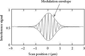
FIGURE 31.9 CSI signal for a single pixel showing the modulation envelope.
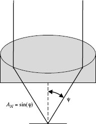
FIGURE 31.10 Definition of numerical aperture (NA), denoted AN.
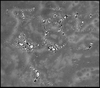
FIGURE 31.11 Images of interference fringes on a highly textured surface structure using spectrally broadband illumination. Interference phenomena localize to a common surface height, allowing for a topography measurement simply by the detection of an interference effect.
At low NA, a serviceable conceptual model of a CSI signal modifies Equation 31.1 to read
where now the magnitude of the cosine modulation is a Gaussian envelope. The constant A is the phase gap between the modulation peak position and the central bright fringe of the interference pattern, resulting from the combined phase shift and phase dispersion effects of the optical properties of the sample material as well as the interferometer optics themselves. The standard deviation σ of the modulation envelope is one-half the inverse of the standard deviation of the optical spectrum, assuming again for the sake of this conceptual model that the light source has a perfectly Gaussian spectral distribution with wavenumber. Although the concept of a slowly modulated carrier signal is only an approximation corresponding to idealized conditions, Equation 31.11 is a useful picture for many signal processing strategies based on the concept of a systematic search for the peak fringe contrast.
As a starting point for algorithm development, we observe that any PSI algorithm can be rearranged to provide a measurement of fringe contrast, allowing for the calculation of the modulation envelope shown in Figure 31.9 by sliding the starting frame for the algorithm along the scan position for the recorded signal [35,36]. This sliding-window PSI method consists of taking the sum of the squares of the numerator and denominator of the PSI algorithm, which are proportional to the sine and the cosine of the interference phase, respectively, so as to calculate the square of the fringe contrast or modulation strength M. For the 3-frame algorithm of Equation 31.7, we then have
The value of M determined from repeated application of this formula traces out the modulation envelope. The next step is to locate the envelope peak, which we identify as the scan position ζ for which ζ = h and consequently we have a measure of local surface height. Clearly we can expect improved results with PSI algorithms that employ more data frames, ultimately leading to algorithms that are nearly as long as broad as the CSI signals themselves [37]. Alternative approaches include hardware [38] or software demodulation [39] specifically oriented toward rapid evaluation of signal strength.
In part because the coherence-based method is based on an evaluation of the modulation envelope, which varies slowly with scan position, it has inherently greater height-equivalent noise than conventional PSI, which leverages the rapidly changing interference fringes themselves. To overcome this limitation, we can calculate the interference phase θ = hK at the envelope peak by interpolation of the evolving phase values over the range of scan positions ζ. This technique provides two measurements of the same height h: one that leverages the high precision of phase measurement, and the other, based on fringe contrast, that is free of any height range limitations related to the 2π problem. Indeed, for most practical configurations, the phase measurement is an order of magnitude lower in noise on smooth surfaces. So it is natural to consider combining the two measurements into a single, final topography map having the benefits of both approaches [36,40].
In practice, combining phase and coherence data for higher precision is not as straightforward as one might think. The first issue encountered, which is actually quite an interesting one, is that the fundamental metric of measurement is different for the two methods. On the one hand, the phase data scales to height according to the inverse of the fringe frequency K, which we usually calculate based on our knowledge of the wavelength and optical geometry. The coherence-based topography, on the other hand, is calculated based on the scan position ζ, which has nothing whatsoever to do with the wavelength. The two calculations are sufficiently different that many early CSI instruments separated the two methods into two distinct measurement sequences, the first using broadband light and the fringe contrast method, and the second using narrowband light and traditional PSI [30,41].
A way out of this dilemma is to link both the coherence and phase calculations together to the same length scale by using a common data reduction method for both. In the frequency domain analysis (FDA) method commercialized in the early 1990s, this is achieved by setting aside the calculation of the fringe contrast envelope and working entirely in the frequency domain by means of a discrete Fourier transform of the CSI signal [33,42]. The result is a series of Fourier coefficients of phases ϕv associated with fringe frequencies Kv scaled according to the known or calibrated scan step between camera data acquisitions. These Fourier phases are
and the coherence-based estimation hC of surface height h is now given by the phase slope
estimated from a least-squares linear fit to those discrete values ϕv, Kv for which the Fourier magnitude is the strongest (see Figure 31.12). This same linear fit provides a mean phase value at a chosen center frequency K0
equivalent to a PSI measurement using all of the data frames that have nonzero signal modulation. To calculate the final height value, we apply
where
In Equation 31.16, the round function returns the nearest integer to its argument, and the brackets 〈 〉 represent a field average [33]. The shape of the source spectrum, the mean wavelength, and the specifics of the optical geometry are no longer needed for scaling surface heights.
As is the case with PSI, CSI has enjoyed a great deal of attention at the algorithm level and there are many data processing alternatives to the example PSI and FDA methods described here. Somewhat confusingly, these developments have led to a pantheon of pseudonyms for CSI according to the specifics of the data reduction. ISO 25178–604 list 16 alternative names for CSI, ranging from high-definition vertical scanning interferometry (HDVSI) to scanning white light interferometry (SWLI) [32]. The most recent entry in the nomenclature library is full-field time-domain optical coherence tomography (OCT), a method derived from single-point OCT systems but now using a camera in a manner that is in many ways parallels traditional CSI.
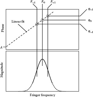
FIGURE 31.12 Illustration of the frequency-domain analysis method. A digital Fourier transform of the CSI signal (Figure 31.9) yields a magnitude and phase for each Fourier coefficient as a function of fringe frequency. A linear fit to the unwrapped phase data weighted by magnitude provides the surface topography information using the scan speed to scale the surface heights.
31.3 INSTRUMENT DESIGN FOR INTERFERENCE MICROSCOPY
31.3.1 LIGHT SOURCE AND DETECTION
The illumination for interference microscopes may be incandescent, such as a halogen lamp, a discharge lamp, or more commonly in modern instruments, an LED or other solid-state device. Some but not all instruments have light stops for adjusting the size of the illumination field as well as the illumination aperture in a Köhler geometry, which images the light source into the pupil of the objective.
Microscopes for quantitative microscopy employ a two-dimensional array camera for electronic image capture and computer processing. Areal measuring systems may use conventional cameras of the CCD or CMOS type, with a format ranging from 640 × 480 pixels to over 4 million pixels [43]. In addition to field size, the data acquisition speed in camera frames per second, the linearity, and quantum well size are of primary importance. Additional capabilities of interest include pixel binning for lower noise or faster acquisition speeds.
Modern microscopes are dominantly of the infinite conjugate type, with telecentric imaging, and magnification determined by the combined action of the objective and the tube lens [44]. The net magnification figure relates to the relative size of an image feature on the camera to the actual or object feature, and is the product of the objective magnification and the magnification of the imaging optics, often referred to as either the tube lens or the optical zoom lens. Both the objective and the imaging lens magnifications are given by the ratio of the focal length to a common fixed value: conventional imaging objectives from Meiji, Leica, and Nikon all use 200 mm, while Olympus uses 180 mm, and Zeiss 165 mm. Interference objectives often use these lenses and will carry these or system-corrected magnifications as engraved indications. The physical size of the camera chip determines the FOV corresponding to a given magnification. For example, if the product of the objective and tube lens magnifications is 10×, then the FOV will be 10× smaller than the physical size of the camera-sensing area.
The Mirau interference objective in Figure 31.7 has a partially transmitting beamsplitter and a small reflecting reference surface far outside the focal plane of the objective. This interferometer is specifically designed to work with diffuse illumination that fills the pupil of the microscope objective: the illumination and imaging light paths go around the reference mirror, which is sometimes referred to as a central obscuration.
Modern instruments allow for interchanging objectives of various magnifications and interferometer type. The Mirau objective of Figure 31.1 is common for magnifications of 10× and above, while at lower magnifications, the Michelson type shown in Figure 31.13 is preferred. Some high-magnification systems that demand larger working distance than the Mirau are served by the Linnik objective [45], similar to the Michelson but constructed from two matched microscope objectives, one for the reference and one for the measurement path. Figure 31.14 illustrates a collection of modern interference objectives operating over a range of magnifications.
As shown in Figure 31.1, adjusting the position of the objective vertically brings the sample into focus. In such a configuration, the focus adjustment is synchronous with an adjustment of the OPD between the measurement and reference paths. The objective itself must be engineered or adjusted so that the OPD is zero and the measurement and reference paths are equal at the position of best focus. At high magnification, this may require making use of a fine-adjustment ring on the outside of the objective. High-magnification objectives often automatically compensate for thermal effects to obviate the need for frequent manual adjustment.
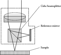
FIGURE 31.13 Michelson-type interference objective.
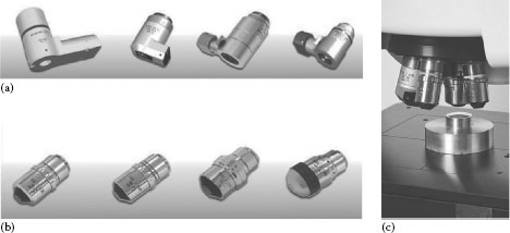
FIGURE 31.14 Modern commercial interference objectives. (a) Michelson objectives, (b) Mirau objectives, and (c) Turreted objectives [46].
Instrument software typically offers fine focus as part automated procedure, although it is still very common to require the user to perform some sort of initial setup involving both focus and tip and tilt adjustment of the sample. There are many alternatives to the focus mechanism of Figure 31.1. Often there is a coarse adjustment mechanism, sometimes referred to as the z stage, which moves the entire microscope assembly up or down; while fine focus is provided by a PZT stage that may also provide the mechanical scanning that is integral to most automated data acquisition and analysis methods. A less common method involves independent actuation of the reference mirror, decoupled from the focus, so that optical path length adjustment becomes independent of focus position [47,48].
An additional consideration in interferometer design for spectrally broadband illumination is the need to balance the amount of dispersive material in the reference and measurement paths. In the Michelson objective of Figure 31.13, this is achieved by using a cube beamsplitter in place of a plate, which would require a compensating element. The cube is fabricated from glass components that are nominally of the same shape and thickness. Similar considerations drive the design of Mirau objectives, which are usually manufactured with the beamsplitter and the reference mirror cut from the same piece of glass to match their thicknesses. Alternatively, the beamsplitter may be made of a sandwich of two plates of equal thickness [49]. If the sample is inside a chamber with a transparent window, specialized objectives are available with adjustable compensation in the reference path [50,51,52].
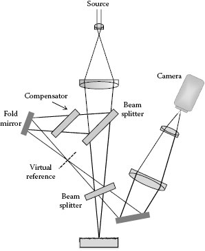
FIGURE 31.15 Interferometer without a physical reference surface in focus.
For all of the interference objectives described so far, the reference mirror is always kept at the focal plane of the objective, while the sample is scanned along the axis orthogonal to the part surface. Proper setup of the instrument requires that the focus for the objective be coincident with the zero OPD position. High-magnification objectives (50×, 100×) are often designed to compensate for shifts in focus position caused by temperature changes.
The sharp focus on the reference mirror means that the measurement is in reality a comparison of the sample with the reference surface, including the high-spatial frequency roughness of the reference. High-precision measurements usually involve calibration of the residual flatness of the form of reference surface [53,54], but the fine-scale roughness is difficult to compensate and can become a source of uncertainty when measuring super-smooth samples. One solution is to arrange the optics so that there is actually no physical surface in the reference arm that is in focus, an example of which is illustrated in Figure 31.15 [55,56].
Complete interferometric microscope systems for surface characterization have a wide variety of configurations depending on the end application. Perhaps the most common is a general purpose or benchtop system, as shown in Figures 31.16 and 31.17. These systems accommodate a wide variety of part types and shapes, and are common in academic, R&D, and general purpose applications. Benchtop configurations include a computer, display, joystick control, and other essential peripherals, often integrated into a custom platform as in Figure 31.18.
For targeted applications in precision manufacturing, where the interferometer must operate close to machinery, an industrial enclosure as shown in Figure 31.19 is appropriate. The enclosure protects the instrument from oils and debris and provides additional acoustic and environmental isolation to improve the metrology. For many such applications, instrument users and providers customize the configuration for specific routine tasks requiring specialized fixtures and staging [58]. The computer interface reduces to a simple pass–fail reporting system, with results reported to an external database that tracks production quality and yield. Semiconductor wafer metrology requires the most demanding and complete automation, with the enclosure and part handling often comprising the largest part of the system cost (Figure 31.20).
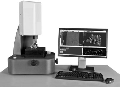
FIGURE 31.16 Bench-top interference microscope with a single objective [57].
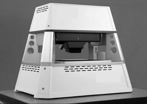
FIGURE 31.17 Bench-top configuration designed for high stability [43].
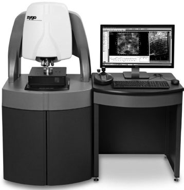
FIGURE 31.18 Integrated platform for general-purpose applications.
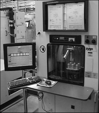
FIGURE 31.19 Industrial interferometry for precision manufacturing.
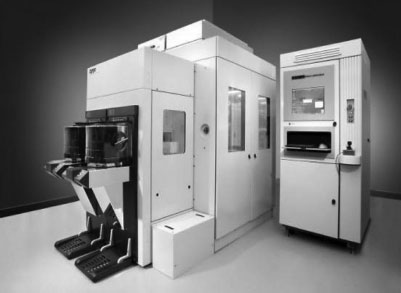
FIGURE 31.20 Fully automated semiconductor wafer metrology using interference microscopy.
FIGURE 31.21 Examples of surface finish having texture characteristics that are evident in the surface topography maps generated by interference microscopy.
One of the strengths of any computerized surface analysis tool is the ability to extract surface details and texture parameters digitally. Common postprocessing steps include the application of filters to highlight particular spatial frequency ranges [59], advanced texture analysis as in Figure 31.21, and extraction of specific form and roughness parameters [60,61,62]. Systems capable of transparent films analysis also provide 3D maps of thickness and refractive index homogeneity.
31.4.1 MODELING OF INTERFERENCE MICROSCOPY FRINGE PATTERNS
The conceptual model of a Michelson interferometer in Figure 31.4 and the accompanying signal models are sufficient for basic ideas, but in reality, the interference signal in a microscope configuration is much more complex and interesting. The spatial extent of the incoherent illumination in the pupil of Michelson and Mirau objectives, the broadband optical spectrum, and the surface structure contribute to shaping the interference signals. These realities can complicate metrology in some cases, while at other times they make it possible to extract additional information beyond surface topography, including material composition, transparent film layers, and optically unresolved surface structure.
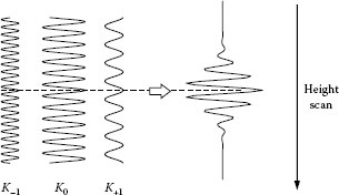
FIGURE 31.22 Conceptual diagram of the incoherent superposition method of synthesizing interference signals for interference microscopy.
A common physical model of the interference process assumes incoherent superposition of ray bundles of differing wavelengths [63]. The signal is the incoherent sum of the interference contributions of the ray bundles passing through the pupil plane of the objective and reflecting from the object and reference surfaces [27,64,65]. Figure 31.22 provides a qualitative understanding of the signal generation process using the concept of incoherent superposition. The summation over a range of frequencies results in a peak signal at a specific scan position where all of the individual interference contributions are mutually in phase, sometimes referred to as the stationary phase point. This is the peak of the modulation envelope shown in Figure 31.9. This concept maps to the frequency-domain analysis method of Figure 31.12, where now each complex Fourier magnitude and phase in Figure 31.12 corresponds to one of the interference contributions of Figure 31.22. The integrations may be performed numerically as part of a mathematical model, as detailed in Ref. [34]. Computational methods such as these allow for prediction of instrument response with variations in optical geometry and surface structure, while allowing for new measurement modes based on model-based analysis [66,67].
One of the uses for signal modeling is the determination of the net fringe frequency of the interference signal for the case where there is a broadband spectrum or a range of incident angles in the illumination. The effect of incident angles is of particular importance to PSI, which relies on the fringe frequency K as the fundamental metric for scaling heights. Traditionally, the effects of the source geometry contribute to an effective wavelength or equivalent wavelength starting from the actual mean wavelength of the light source and using the obliquity factor as a multiplicative correction.
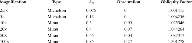
The obliquity factor has been extensively analyzed, and there are a range of approximation formulas for its calculation based uniquely on geometric factors and assumptions regarding the pupil plane light distribution [64,68,69,70,71,72,73]. Signal modeling provides an alternative calculation of the effective wavelength that incorporates the optical spectrum, the system geometry, the shape of the light source [73], and potentially the special characteristics of the object material. The procedure involves direct numerical calculation of the Fourier components followed by centroiding the resulting Fourier spectrum, which provides an accurate determination of the mean wavelength of the final interference signal. Results in Table 31.1 show that the obliquity effect is easily detectable with common low-magnification objectives and is of critical importance at high magnifications, where the obliquity effect can change the equivalent wavelength by 30%.
TABLE 31.1
Obliquity Factor Calculated by Modeling of the Interference signal, Assuming a Fully Filled Objective Pupil, a Dielectric sample, and Circular Polarization
Many high-value devices comprise thin films, some of which may be partially transparent in the wavelength range of an interference microscope. Consequently, a complete surface characterization may entail mapping both the film thickness and the top-surface height variation. At a minimum, we require surface topography–measuring instruments to be compatible with the presence of thin transparent films.
For a PSI instrument in near-monochromatic illumination at low NA, a transparent film on the sample surface presents something of a challenge: the light reflects partially from both the top surface and the underlying substrate, or in the case of multilayer films, from several places within the semi-transparent surface structure. The measurement principle as described so far does not account for this. The potential errors are not intuitive or easy to interpret—the measured surface topography is not the average of the top and underlying surfaces, but rather is some nonlinear function of the film thicknesses and refractive indices. Corrections are feasible if the film thickness and index are well known, but these a priori data are not always available (Figure 31.23).
From the earliest implementations of CSI, it was recognized that a unique benefit of a low-coherence illumination is the ability to distinguish between the multiple surface reflections of a transparent film, provided that the film thickness is greater than the width of the modulation envelope [74,75,76]. For these so-called “thick” films, the multiple reflections from the top surface, substrate, and possibly intermediate layers result in readily distinguishable signals. The location of these signals in the scan history identifies the optical thickness of the film, at least for low-NA applications where we can neglect the competing effect of spatial coherence. Knowledge of the film’s refractive index allows for simultaneous topography and film thickness mapping.
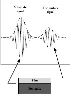
FIGURE 31.23 Multiple CSI signals from a surface film structure.
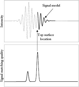
FIGURE 31.24 Method for locating top-surface reflections using a truncated signal model and a least-squares fit [77].
The same concept of signal separation extends with advanced processing to films that are too thin for full signal separation. Figure 31.24 illustrates a method for isolating the top-surface contribution to a CSI signal even when the substrate and top-surface signals are partially merged. The technique consists of a least-squares fit of a signal model that contains only the leading-edge portion of the signal. This method allows for top-surface profiling in the presence of transparent films that are too thin for complete separation of the CSI signals, but still thick enough to identify portions of the CSI signal that are dominated by specific surface reflections [77]. Figure 31.25 compares a 3D top-surface interferometry image with atomic force microscopy (AFM) for a flat-panel display pixel. This sample has transparent films in several areas, with a minimum thickness of 600 nm. A nice feature of this approach is that it does not require any advance knowledge of the material properties of film or embedded features.
Provided that we know the optical properties of our instrument well enough, an effective approach to analyzing thin transparent films is to model the expected response of the instrument to a range of possible film parameters, creating a library of model signals that we compare in their entirety with the experimental signal to find the best match (Figure 31.26). A model-based approach has the advantage of simultaneously providing a direct 3D measurement of film thickness as well as the upper and lower interface profiles. Most systems employ frequency-domain methods, wherein the experimental CSI signals are transformed by Fourier analysis and the complex coefficients are compared to stored library signals to evaluate surface structure [33,78,79,80,81]. Although the library search technique requires detailed system and surface structure modeling, this approach has found applications for specialized high-value production testing, as in the TFT LCD example of Figure 31.27. Film thickness measurement is possible down to 10 nm using this technique.
FIGURE 31.25 Comparison of CSI with AFM measurements of the top surface of a thin film transistor (TFT) of a liquid-crystal display (LCD). The images are 40 μm2. (a) Coherence scanning interferometry and (b) atomic force microscopy [77].
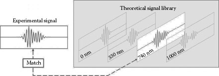
FIGURE 31.26 Model-based films analysis. Experimental CSI signals are matched to precomputed theoretical signals that depend on instrument calibration data and a model of the sample under test, in this example a layer of silicon dioxide on silicon [66].
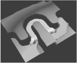
FIGURE 31.27 Map of photoresist thickness near a transistor gate on a TFT LCD panel using model-based analysis. The horseshoe-shaped trench is nominally 400 nm thick and 5 μm wide [66].
The same basic concepts of a model-based library search enable analysis of surface structures smaller than the lateral resolution limits of conventional microscopy. For these techniques, the mathematical approach is necessarily more sophisticated than the simple incoherent superposition model, which implicitly assumes only a nominally flat structure complicated at most by uniform layers of transparent films. The presence of sub-wavelength features requires modeling methods such as rigorous coupled wave analysis (RCWA). These advanced techniques have found application in the semiconductor industry, in some cases using specialized optical geometries where the objective pupil is imaged onto the camera in place of the object surface itself [67,82,83].
31.5.1 GOOD PRACTICE AND INSTRUMENT EVALUATION
Interference microscopes measure a wide variety of surface textures, and real-world performance depends on influence factors such as surface texture, surface slope, thermal drifts, and form distortions related to the interaction of the surface structure with the illumination. Additional factors include measurement procedure and relevant calibrations and adjustments. Consequently, meaningful statements of instrument performance are closely tied to the specifics of the measurement task [84]. Quality control experts have understood this for some time, which is the reason for empirical tests such as the classic test for gage repeatability and reproducibility (GR&R) performed on the part of interest close to the actual conditions of measurement. These tests combine with correlation studies that relate the functional properties of the part to the detected surface structure.
Instrument providers are the primary resource regarding how to get the best performance from interference microscopes for specific tasks, supplemented by good practice guides [85,86], international standards documents [32], and a growing body of literature. A general caution is that published instrument specifications can be misleading and often use nonstandard terminology. Statements related to performance should include a clear procedure for validation, either as a footnote or reference to a national or international standards document that specifies these procedures.
31.5.2 SURFACE TOPOGRAPHY REPEATABILITY
Perhaps the most basic performance characteristic of any metrology task is the measurement noise. As with any metrological characteristic, the measurement noise has several influence factors, some of which may be controllable, such as environmental vibration, air turbulence, acoustic noise, and thermal instability. The instrument noise is usually specified and evaluated according to an example measurement under ideal conditions—a quiet lab, a part chosen to provide good results, such as a polished optical flat with just the right reflectivity for optimal results. This is a close approximation to a test of the intrinsic additive noise that cannot be reduced by control of external influence factors [87]. It is common to see terms such as precision as surrogate specifications for noise, consistent with established vocabulary (VIM Section 2.15 [88]).
A quantitative evaluation of noise consists of evaluating the measurement consistency with repeated trials, without changing anything. For 3D interference microscopes, the most fundamental output is an aerial surface topography map, which shows the height over an array of perhaps a million different surface points corresponding to camera pixels. The surface topography repeatability tells us how close we can expect the indicated height value for a specific sample point (or camera pixel) will repeat if we measure it over and over again [32,87]. The value usually is expressed as a root-mean-square (RMS) value or standard deviation in units of height, and is readily computed from statistics over a full image of surface points.
The simplest repeatability test is to measure a suitable flatness artifact twice, subtract the difference of the two resulting topography maps, and calculate the standard deviation Sq of the difference map [53,89]. The surface topography repeatability, denoted here as the ISO measurement noise NM, is then
For situations where intermittent disturbances such as vibrations may influence the repeatability, or where a more authoritative value is essential, a more reliable statistical approach is to take a large number of repeated measurements of the artifact. Several methods treat the statistics of these multiple measurements to provide a robust estimate of repeatability [90,91].
For interference microscopes, we can often estimate instrument noise based on first principles, at least for the major noise contributors. For most automated interference microscopes in a calm environment, this is random shot noise from the camera. For PSI, the resulting phase noise depends to some degree on the specific PSI algorithm coefficients, but as a general rule, scales inversely with the square root of the number of camera frames used to calculate the phase, as one would expect from random fluctuations [92,93]. For a single data acquisition using the 12-frame sinusoidal phase shifting algorithm of Equation 31.8, the theoretically predicted noise level for a 600 nm wavelength without any lateral filtering is
where σ is the signal to noise ratio, defined here as the standard deviation of the random intensity noise divided by the amplitude of the interference signal [20]. A typical intensity noise σ is 1.5%, which, after 25 averages provides a surface topography repeatability of 0.1 nm, independent of magnification. This is a common specification value for PSIs, consistent with the qualitative “subnanometer” characterization of the technique.
For noise contributions that are entirely uncorrelated between image pixels, lateral smoothing or S-filter as described in ISO 25178–3 can considerably improve the surface topography repeatability value [59,60]. Surface filtering is a legitimate postprocessing step in areal surface topography and may even be mandated for correlation to other measurement techniques that may have intrinsically different spatial frequency response [94]. For a formal specification, however, it is essential to clearly state any lateral filtering operations as these may have an influence on other specifications such as lateral sampling and resolving power.
Surface topography repeatability improves with averaging or by using a PSI algorithm that requires more camera frames, following the observation that random noise declines as the square root of the number of sample values. Increased averaging comes at the cost of data acquisition time; therefore, a specification for the surface topography repeatability should include the corresponding time to measure. This is consistent with common engineering practice, which expresses random noise as a value divided by . For example, a stated surface topography repeatability number for a phase-shifting type interference microscope might be 0.1 nm. This number may require 25 averages of individual measurements, each one of which requires 12 camera frames, for a total of 300 frames. With a 75 Hz camera, the fastest possible measurement using continuous data acquisition would be 4 s, or . The 0.25 Hz frequency associated with the 0.1 nm specification allows the user to predict behavior for longer or shorter data acquisition times, following the square root rule, and to make adjustments to achieve a specific noise target consistent with throughput requirements.
For CSI, specifying instrument noise for a given time interval is complicated somewhat by the availability of multiple modes and selectable height-scanning range. For any single measurement, representative performance values without lateral filtering and with a data sampling rate of four camera frames per interference fringe are 3 nm for methods based on the modulation envelope and 0.4 nm for measurements based on a phase evaluation to improve precision [33]. The phase performance is consistent with the example calculation following Equation 3.19, and the larger CSI value is consistent with the differential nature of this measurement. The acquisition time for a single measurement scales inversely with the scan rate, which for a 100 Hz camera and a 600 nm wavelength would be 7.5 μm/s. These values together with the desired height range allow for an estimate of the surface topography repeatability as a function of total data acquisition time. As is the case with any measurement dominated by random noise, the CSI result can be further reduced with averaging of final height maps, as shown by the experimental data of Figure 31.28.
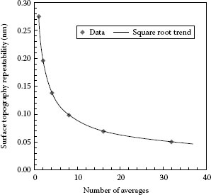
FIGURE 31.28 Noise reduction in a CSI instrument using measurement averaging [91].
31.5.3 VIBRATION AND ENVIRONMENTAL EFFECTS
Not usually found on an instrument specification sheet are several important error sources that can significantly influence the measurement performance and that potentially far outweigh the basic surface topography repeatability specification in the evaluation of measurement uncertainty. One of these contributors is vibration. Instruments based on interferometry are almost invariably equipped with systems to dampen or isolate unexpected mechanical motions to overcome the vibration sensitivity of time-sequenced phase shifting [95,96]. The residual errors depend on the vibrational frequency [6,32,95,97], with low-frequency vibrations associated with form errors and high-frequency vibrations at specific frequencies contributing to ripple errors at twice the spatial frequency of the interference fringes. Figure 31.29 illustrates these effects using experimental CSI data at 20× magnification for a flat mirror. Figure 31.29a shows the orientation of the interference fringes. Without vibration, the measured surface roughness shown in the upper-right topography image is 1 nm rms. The errors caused by environmental vibrations shown in the lower-left and lower-right images for the same surface are 4 nm rms for low- and high-frequency vibrations, respectively, although the effect on the measured surface form is clearly different. Even though the direction of vibration is dominantly along the scanning or z direction, the resulting errors are phase dependent and therefore follow the orientation of the fringes in the intensity image. This is particularly evident in the high-frequency vibration ripple errors shown in Figure 31.29d. The magnitude of the error for the same vibrational amplitude varies significantly with vibrational frequency, with peak sensitivity for ripple errors at one-half the camera frame rate when the camera sampling rate is four frames per interference fringe.
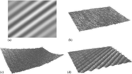
FIGURE 31.29 Experimental demonstration of potential errors caused by vibration in a traditional CSI instrument. Newer instrument employ technologies to reduce these effects and make it easier to use interference microscopy in production environments. (a) Intensity image, (b) 3D topography, (c) low frequency vibrations, and (d) high frequency vibrations [98,99].
Knowledge of vibrational frequency spectrum for a given environment can lead to strategies for avoiding these frequencies and improving performance. More ambitiously, several nontraditional approaches to PSI data analysis do not require precision in the phase shifts and are more tolerant of vibrations and other unexpected disturbances [100,101,102], Vibration-tolerant software relies heavily on the ever-increasing data processing power using statistical or maximum likelihood analyses. These techniques, when combined with additional hardware and software mitigation strategies, provide improvements over conventional interferometry of more than a factor of 100. Vibration robustness allows optical instruments to function in environments where conventional interferometers and precision stylus tools would fail, helping to bring interferometers from the quality control laboratory closer to the production floor [98,103].
Further to the goal of reducing vibration sensitivity, it has been proposed to use multiple detectors to acquire phase-shifted images simultaneously in an interference microscope using carrier fringes as in holography [104], or polarization encoding of the reference and measurement beams [105,106]. Such methods duplicate PSI functionality without time-dependent phase shift, providing near-instantaneous 3D surface topography measurements. Such methods allow for video-rate imaging of moving objects such as live cells [107], but have some limitations related to the need for polarized optics.
31.5.4 OPTICAL EFFECT OF SURFACE MATERIALS
The optical properties of the materials that make up the object surface influence the shape and position of the interference signal within the data acquisition scan. As a general rule of thumb, the phase of the interference pattern depends on the phase change on reflection (PCOR) of the surface material, while the rate of change of PCOR or dispersion influences the position of the modulation envelope [32,42,108]. The shift in the envelope position is the same phenomenon as the offset experienced in multiple-wavelength interferometry when there is refractive index dispersion [109,110]. If the object surface material is uniform, there is generally no obvious way to distinguish between variations in PCOR and actual height differences.
Table 31.2 provides examples of the change in apparent surface height as determined from signal modeling, for a 560 nm light source with a 110 nm bandwidth, at low NA. In some cases, the envelope shift can be small while the phase shift is large, as is the case for example with copper. The amount of shift can vary significantly depending on the wavelength and the bandwidth, particularly for materials such as gold that have absorptions and nonlinear dispersion in the visible wavelength range. For other materials such as silver, the envelope shift is nearly identical to the phase shift. The amount of phase shift is only weakly dependent on the spectral bandwidth for most materials, but the envelope shift can be a strong function of both bandwidth and NA. In the limit of very high NA (above 0.6), the envelope position is dominated by focus effects that are less sensitive to material properties. This last observation has been proposed as a means of detecting and quantifying the PCOR [71].
TABLE 31.2
Effect of Material Phase Change on Reflection on Measured Surface Heights at Low NA for a Wavelength of 560 nm
Material |
Envelope Shift (nm) |
Phase Shift (nm) |
Bare glass |
0.0 |
0.0 |
Silicon |
−2.4 |
−0.2 |
Aluminum |
−9.5 |
−12.5 |
Chrome |
−15.5 |
−13.4 |
Platinum |
−11.0 |
−17.9 |
Copper |
−1.1 |
−30.4 |
Cobalt |
−11.0 |
−18.0 |
Silver |
−25.9 |
−25.1 |
Some software packages allow for calculation of the PCOR using a known refractive index and a simple analytical formula [31], although these calculations are valid only for low NA and are of no value in determining the envelope shift. The only accurate way of calculating dissimilar materials effects is through numerical modeling that includes the full geometry of measurement and accurate data regarding the wavelength-dependent index of refraction. Alternatively, it is often expedient to evaluate the effects of PCOR empirically, using known structures [111]. This experimental determination may involve metrology methods such as stylus profilometry that are less sensitive to PCOR and transparent film effects [112].
The resolving power or lateral resolution of a 3D metrology instrument quantifies its ability to separate adjacent features on the surface. As an example, Figure 31.30 shows on the right two closely spaced trenches formed by patterning silicon on a quartz substrate [113]. The interference microscopy 3D image on the left-hand side of the figure shows that there are indeed two lines present, although they appear blurred at this high magnification. As the center-to-center separation between the lines decreases, the resolving power of the instrument becomes a limiting factor in determining if the two lines are clearly separated in the 3D image. If the resolving power is insufficient, the two lines will simply appear as one large line.
In conventional noninterferometric imaging systems with incoherent illumination, it is common for a single number to define the resolving power. According to the Sparrow criterion borrowed from optical imaging, as features get closer together, the lateral resolution is the center-to-center separation between two surface features at which the instrument is no longer able to distinguish these features as separate images. For a diffraction-limited microscope with an incoherent light source, the Sparrow limit of a conventional imaging microscope for two source points is
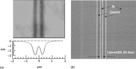
FIGURE 31.30 (a) 3D CSI microscope image of two parallel trenches of a 200 nm linewidth standard from Supracon AG, using a 100× Mirau objective with an NA of 0.85. (b) Corresponding scanning electron microscope image, showing the linewidth and the sample structure. The center-to-center separation of the lines is 440 nm [114].
where Rl is the center-to-center spacing of the features, and as previously defined previously in Figure 31.10, AN is the NA. To take advantage of this diffraction-limited resolution, the camera pixel size in object space must be much smaller than Rl, otherwise the resolution is said to be camera limited.
Turning now to areal surface topography measurement using optical methods, it is not obvious that the traditional imaging definitions such as the Sparrow criterion should apply [114]. The principle of interferometric surface metrology, for example, relies on a simple relationship between phase and surface height, as in Equation 31.3. When we add together optical wavefront contributions from closely spaced surface features, the phase shifts caused by the various surface heights do not directly add together. Instead, it is the complex wavefront amplitudes that are summed. When the feature separations are close to the traditional resolving limit of the optical imaging system, we cannot assume a linear response.
The concept of imaging resolution as applied to 3D optical instruments is recovered if we restrict ourselves to small feature heights, defined as heights for which the instrument response is linear. The definition of “small” follows from approximations similar to the small-angle limit of the sine function and translates to a few tens of nanometers for common visible-wavelength interference microscopes [116]. This limitation does not restrict the overall useable height measurement range of the instrument, which may be several tens or even hundreds of microns; rather it applies to sharp edges and features that are closely spaced on the scale of the lateral resolution of the instrument. If we respect this limitation of small heights for closely spaced surface features, we can leverage traditional and familiar 2D imaging definitions to describe the 3D topographical measurement properties. Indeed, it can be shown that in the limit of small heights, the well-known modulation transfer function (MTF) has a meaningful analog in the instrument transfer function (ITF) for 3D metrology [115]. Figure 31.31 illustrates this correspondence for a CSI instrument for a 20× Mirau objective, a filled 0.4 NA pupil, 570 nm wavelength. The spatial frequency for which the MTF reaches zero is the Abbe limit, which is close to the Sparrow limit. The close similarity between MTF and ITF breaks down for highly aberrated or defocused optical systems, for which 3D topography may be distorted in a way that has no direct analog in conventional optical imaging.
It is evident that paths to higher resolving power lie with smaller wavelengths λ, which may be difficult to realize in practice, or with increased NA, which is more commonly how instruments achieve high-resolving powers. High-NA objectives are more common at higher magnifications, and therefore there is a sensible tradeoff between FOV and NA for available interference objectives. Table 31.3 provides a list of common objectives and their resolving powers.
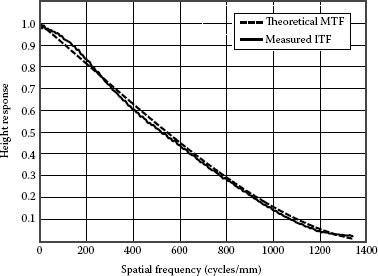
FIGURE 31.31 Comparison of the theoretical optical MTF and the measured 3D topography ITF for a CSI instrument at 20×. The Sparrow criterion limit is 670 nm or 1490 cycles/mm [115].
TABLE 31.3
Specifications of Selected Modern Commercial Interferometer Objectives, Including the Lateral Resolution as Calculated according to the Sparrow Criterion of Equation 31.20 and Pixel Size for a 2× Imaging Lens
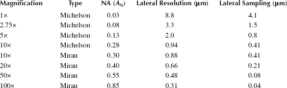
Source: Zygo Corporation, NexView Optical Profiler, Specification sheet, 2013.
In addition to these optical effects, real instruments introduce additional influences on the ITF related to the electronic detection, conversion to 3D images, and postprocessing. The magnification and camera format define the lateral sampling, usually expressed in terms of pixel spacing in object space. Table 31.3 includes lateral sampling for a camera and imaging system providing an 8.2 μm pixel size in object space when using a 1× imaging lens. Ideally, the lateral sampling is fine enough to avoid aliasing high frequencies beyond the Nyquist frequency, a requirement that translates to a lateral sampling period that is equal to or less than half the lateral resolution. Particularly at low magnifications, the pixel size itself further attenuates the ITF with frequency according to a sinc function, with the first zero at a spatial period equal to the pixel size.
Postprocessing, including in particular lateral filtering, has an obvious and significant effect on the ITF. Instrument software invariably includes options to extract textures or surface form. ISO 25178–3 defines areal filters according to some basic rules on how to set the size of the primary surface and the sampling distance [60]. In addition to attenuating selected frequencies, given sufficient signal to noise, postprocessing can amplify portions of the ITF to sharpen details that are otherwise only marginally resolved [117]. ITF correction is also feasible for derived parameters such as the measured power spectral density (PSD) by means of multiplicative corrections to the measured results [118].
A number of methods are available for evaluating lateral resolution experimentally, using well-characterized sample structures. One approach involves an artifact similar to that shown in Figure 31.30, with a selection of line pairs to establish the distance at which the line images merge. Some linewidth artifacts [119] can serve this purpose; although it is essential to not confuse the width of individual lines with feature separation. Referring to Figure 31.30, the center Si line is 200 nm wide, much smaller than the Sparrow limit identified in Table 31.3; but the center-to-center spacing of the trenches that form this line is 440 nm, consistent with the calculated 310 nm resolution limit for 0.85 NA at visible wavelengths. Another caution is that the traditional Sparrow number as calculated from Equation 31.20 applies to source points, and line pairs are somewhat easier to resolve [120].
For ITF characterization, it is often more reliable to measure gratings or arrays of multiple lines at a calibrated spatial period rather than to examine isolated line pairs. Variations on this concept include chirped-frequency gratings [121] and the 3D version of the Siemens star [122,123]. Another approach is an edge feature, which allows for direct measurement of the edge-spread function, which by Fourier methods can be expressed as an ITF [114,116,124,125]. This method provided the experimental ITF data shown in Figure 31.31 [115].
31.5.6 FIELD OF VIEW AND SLOPE ACCEPTANCE
In some applications, a larger FOV is more important than lateral resolution, leading to the use of low-magnification objectives with correspondingly reduced NA. The FOV follows from Table 31.3 by multiplying the lateral sampling by the number of pixels. For example, if the camera has a square array of 1000 × 1000 pixels, the field of view at 1× would be 8.2 mm. For these low-NA objectives, it may not be possible to capture specularly reflected light from high slopes.
A first option for large areas and steep surface slopes is to take a sequence of relatively high-magnification, small FOV images and reconstruct or stitch a larger image from these multiple measurements [126]. The benefit of this method is that it simultaneously provides a large FOV and detailed, high-resolution information, as illustrated in Figure 31.32.
As a second option, many modern systems have sufficient sensitivity to measure surface geometry using only the small amount of scattered light from highly inclined, smooth surfaces, as illustrated in Figure 31.33. The required amount of scattered light in these systems can be surprisingly small—a return of 0.05% of the incident light is sufficient, enabling a slope acceptance of up to 86° even at low magnifications [127].
The overall uncertainty of the measured surface topography depends on the height response of the instrument (Figure 31.34). The importance of calibration and verification of the height response depends to a large degree on the principal application for the interferometer: If the metrology task is to characterize roughness or texture, an uncertainty in the overall scaling of surface heights of a few percent may not be a significant factor in the usefulness of the result. However, if the principal task is to measure discrete feature heights of several microns with an uncertainty of a nanometer, then the height scale is of primary importance.
FIGURE 31.32 Large FOV image constructed from multiple CSI images of smaller size. The inset shows the level of detail provided by this stitching method.
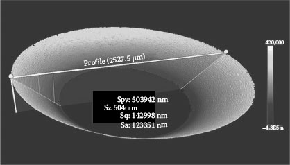
FIGURE 31.33 Image with high slopes using only scattered light at low NA. This machined-metal conical valve seal has a depth is 0.5 mm while the diameter is 2.5 mm.
Common practice is to establish the scaling factor or amplification coefficient for surface heights during manufacture. For a PSI instrument, for example, the illumination wavelength combined with the calculated or experimentally determined obliquity factor (Table 31.1) provides the equivalent wavelength for converting interference phase to surface height. For a CSI instrument, a capacitance or similar high-stability gage governs the scan rate. The manufacturer calibrates the capacitance gage, the associated electronics, and the resulting closed-loop mechanical response during assembly using traceable length metrology such as a laser displacement interferometer.
Standard artifacts such as step heights or coarse gratings facilitate verification of the height scale by end users and are common accessories for areal surface topography instruments [128,129,130]. These artifacts or material measures carry a certification from a national metrology institute or commercial enterprise equipped with reference metrology [131]. If the measured step height consistently falls outside the certified uncertainty boundaries of the step height standard, this may warrant adjustment of the height scale, or alternatively, the service or recalibration by the manufacturer.
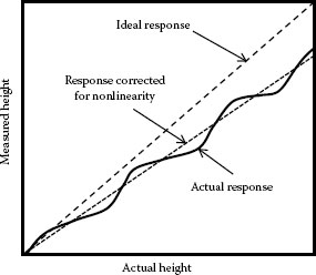
FIGURE 31.34 Height response curves, showing the actual response, the response corrected for nonlinearity, and the ideal linear response with the correct amplification coefficient.
The linearity of the height response of an interferometric microscope is an intrinsic property of the instrument and is more difficult to calibrate and adjust in the field than the height scale. For PSI instruments, the main source of nonlinearity is cyclic error, caused for example by an incorrect phase shift between camera frames, resulting in an error that is periodic with interference phase. For CSI instruments, nonlinearity corresponds to a variation in the OPD scan velocity as a function of scan position. Nonlinearity is usually characterized and corrected during manufacture, and the outcome is a specification such as maximum permissible error. Measurements of several step heights of different size [129], measurements of a small step at various positions in the scan, or external measurements of scan velocity using reference metrology [132] can validate the linearity specification or indicate a problem that requires service.
Another approach to traceable calibration of the height response is to embed the realization of the meter directly into the instrument design. In the evaluation of optical surfaces using laser Fizeau interferometry, for example, there is no need for factory calibration or for transfer artifacts, as the measurement principle is linked to the HeNe or other laser wavelength with a known uncertainty [133]. In some instruments, additional hardware integrates a laser displacement gage into the mechanical scanning system of a CSI microscope [132,134,135], allowing for continuous, independent calibration of the amplification factor and correction for nonlinear response.
With some notable exceptions [119], interference microscopes measure surface topography with respect to a flat datum surface, established and influenced by the combined effects of the reference surface and the optical system. The imaginary topography detected by the instrument when viewing a hypothetical perfect flat part is the residual flatness, which essentially is the height bias as a function of image position. Instrument makers do not usually specify the residual flatness, with the expectation that the end user will calibrate for this error source in situ using a prescribed procedure on a standard artifact such as a silicon carbide reference flat [54]. The result is a system error file that is subtracted from all subsequent measurements [136]. The procedure may require a sequence of multiple measurements with small lateral displacements of the artifact so as to average out the artifact roughness [53].
So far, we have established that interference microscopes under well-controlled conditions have height-equivalent noise levels well below 1 nm for less than a second of data acquisition time and can be calibrated in height response using primary standards based on the wavelength of light, transfer indicators such as capacitance gages, or standard artifacts from NMIs. Keeping these facts in mind, it can be surprising that the lateral resolution and height response for some surface shapes and textures differs from by amounts far greater than the calculated uncertainties after calibration [137]. In some cases, researchers have observed large differences in interference microscope results depending on the data processing mode [138]. In other cases, average amplitude or Ra values measured with CSI have disagreed with stylus measurements on roughness specimens by as much as a factor of two [139].
It has been shown that anomalous results can be overcome in many cases by switching from CSI to PSI measurement modes where feasible [138] or by using CSI data analyses that make use of phase information to improve measurement results on optically smooth parts [42,140]. Figure 31.35 illustrates the improvements afforded by using phase information to reduce the noise level and eliminate measurement errors near the sharp edges of a square profile grating. Modern instruments increasingly incorporate methods to reduce or to compensate for CSI distortions for all surface textures without changing measurement modes, to simplify the instrument setup and operation. The surface profile of Figure 31.36, for example, compares a CSI profile directly with a mechanical stylus profile on a standard roughness specimen, after application of identical filter limits. Figure 31.37 shows the results on Rubert sinusoidal roughness specimen numbers 543, 542, 529, 531, 528, 530, 527, and 525 at 20× and 50× magnifications [99]. Somewhat more ambitious are promising efforts to model the origins of profile distortions and to correct them in postprocessing in a general way [141].
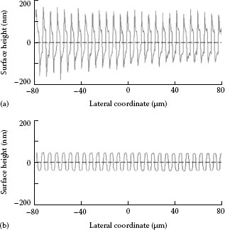
FIGURE 31.35 (a) A particularly alarming example of profile distortions in a traditional CSI microscope for a square-profile 44 nm amplitude grating, viewed at 40× magnification and at 0.4 NA. (b) Improved profile fidelity achieved by incorporating interference phase.
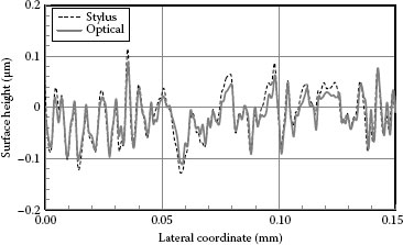
FIGURE 31.36 Comparison of mechanical stylus and CSI optical results at 50× for a Rubert & Co number 502 specimen [99].
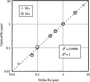
FIGURE 31.37 Comparison of interferometric optical measurements of average roughness Ra for a series of standard roughness specimens. The diagonal line represents perfect correlation [99].
Automated interference microscopy is an established technique for 3D surface topography, transparent films analysis, and texture characterization. Chief attributes of the technique are high sensitivity to surface topography over all magnifications, detailed surface structure analysis including transparent films, and advanced digital postprocessing. The technology continues to evolve, with particular areas of interest in semiconductor yield enhancement [142], industrial quality control on the production floor [58], and biological imaging [107,143]. Further advancements for current research include improving lateral resolution, environmental robustness, measurement speed, profile fidelity, correlation, and ease of use.
1. Sommargren, G. E., Optical heterodyne profilometry, Applied Optics 20, 610, 1981.
2. Wyant, J. C., Koliopoulos, C. L., Bhushan, B. et al., An optical profilometer for surface characterization of magnetic media, Transactions ASLE 27, 101–113, 1984.
3. Koliopoulos, C. L., Interferometric optical phase measurement techniques, PhD dissertation, University of Arizona, Tucson, AZ, 1981.
4. Wyant, J. C., Koliopoulos, C. L., Bhushan, B. et al., Development of a three-dimensional noncontact digital optical profiler, Journal of Tribology 108, 1, 1986.
5. Dresel, T., Häusler, G., and Venzke, H., Three-dimensional sensing of rough surfaces by coherence radar, Applied Optics 31, 919–925, 1992.
6. de Groot, P., Coherence scanning interferometry, in Optical Measurement of Surface Topography, R. Leach (ed.), Chapter 9, pp. 187–208 (Springer Verlag, Berlin, Germany, 2011).
7. Hariharan, P., Optical Interferometry (Academic Press, San Diego, CA, 2003).
8. Page, D. A., Interferometry, in Handbook of Optical Metrology, T. Yoshizawa (ed.), Chapter 6, pp. 191–218 (CRC Press, Boca Raton, FL, 2009).
9. Pedrini, G., Holography, in Handbook of Optical Metrology, T. Yoshizawa (ed.), Chapter 7, pp. 219–240 (CRC Press, Boca Raton, FL, 2009).
10. Wyant, J. C., Use of an ac heterodyne lateral shear interferometer with real-time wavefront correction systems, Applied Optics 14, 2622, 1975.
11. Greivenkamp, J. E., Generalized data reduction for heterodyne interferometry, Optical Engineering 23, 234350, 1984.
12. Bruning, J. H., Herriott, D. R., Gallagher, J. E. et al., Digital wavefront measuring interferometer for testing optical surfaces and lenses, Applied Optics 13, 2693, 1974.
13. Freischlad, K. and Koliopoulos, C. L., Fourier description of digital phase-measuring interferometry, Journal of the Optical Society of America A 7, 542, 1990.
14. Surrel, Y., Design of algorithms for phase measurements by the use of phase stepping, Applied Optics 35, 51–60, 1996.
15. Strojnik, M., Hanayama, R., Hibino, K. et al., Error estimation of phase detection algorithms and comparison of window functions, Proc. SPIE 8511, 84930J-1–84930J-8, 2012.
16. Schreiber, H. and Bruning, J. H., Phase shifting interferometry, in Optical Shop Testing, D. Malacara (ed.), pp. 547–666 (John Wiley & Sons, Inc., Hoboken, NJ, 2006).
17. Sasaki, O., Okazaki, H., and Sakai, M., Sinusoidal phase modulating interferometer using the integrating-bucket method, Applied Optics 26, 1089–1093, 1987.
18. Dubois, A., Phase-map measurements by interferometry with sinusoidal phase modulation and four integrating buckets, Journal of the Optical Society of America A 18, 1972, 2001.
19. de Groot, P., Design of error-compensating algorithms for sinusoidal phase shifting interferometry, Applied Optics 48, 6788, 2009.
20. de Groot, P., Error compensation in phase shifting interferometry, Patent 7,948,637, 2011.
21. Ghiglia, D. C. and Pritt, M. D., Two-Dimensional Phase Unwrapping, Theory, Algorithms, and Software (John Wiley & Sons, New York, 1998).
22. Poole, S. P. and Dowell, J. H., Application of interferometry to the routine measurement of block gauges, in Optics and Metrology, P. Mollet (ed.) (Pergamon Press, New York, 1960).
23. Pluta, M., Microinterferometry, in Advanced Light Microscopy, Vol. 3, Measuring Techniques, Chapter 16, pp. 317–506 (Elsevier, Amsterdam, the Netherlands, 1993).
24. Creath, K., Step height measurement using two-wavelength phase-shifting interferometry, Applied Optics 26, 2810, 1987.
25. de Groot, P., Three-color laser-diode interferometer, Applied Optics 30, 3612, 1991.
26. Deck, L. and Demarest, F., Two-color light-emitting-diode source for high-precision phase-shifting interferometry, Optics Letters 18, 1899, 1993.
27. Davidson, M., Kaufman, K., and Mazor, I., The coherence probe microscope, Solid State Technology 30, 57–59, 1987.
28. Balasubramanian, N., Optical system for surface topography measurement, USPTO Patent 4,340,306, 1982.
29. Kino, G. S. and Chim, S. S. C., Mirau correlation microscope, Applied Optics 29, 3775,1990.
30. Caber, P. J., Martinek, S. J., and Niemann, R. J., New interferometric profiler for smooth and rough surfaces, Proceedings of SPIE 2088, 195–203, 1993.
31. Schmit, J., White-light interference 3D microscopes, in Handbook of Optical Dimensional Metrology, K. Harding (ed.), Chapter 10, pp. 395–418 (Taylor & Francis, 2013).
32. ISO, 25178–604: Geometrical product specification (GPS)—Surface texture: Areal—Nominal characteristics of non-contact (coherence scanning interferometric microscopy) instruments (International Organization for Standardization, Geneva, Switzerland, 2013).
33. de Groot, P. and Deck, L., Surface profiling by analysis of white-light interferograms in the spatial frequency domain, Journal of Modern Optics 42, 389–401, 1995.
34. de Groot, P. and Colonna de Lega, X., Signal modeling for low-coherence height-scanning interference microscopy, Applied Optics 43, 4821, 2004.
35. Larkin, K. G., Efficient nonlinear algorithm for envelope detection in white light interferometry, Journal of the Optical Society of America A 13, 832, 1996.
36. Cohen, D. K., Caber, P. J., and Brophy, C. P., Rough surface profiler and method, US Patent 5,133,601, 1992.
37. de Groot, P., Method and system for analyzing low-coherence interferometry signals for information about thin film structures, Patent 7,321,431, 2008.
38. Caber, P. J., Interferometric profiler for rough surfaces, Applied Optics 32, 3438–3441, 1993.
39. Chim, S. S. and Kino, G. S., Three-dimensional image realization in interference microscopy, Applied Optics 31, 2550–2553, 1992.
40. Chim, S. S. C. and Kino, G. S., Phase measurements using the Mirau correlation microscope, Applied Optics 30, 2197, 1991.
41. Ai, C. and Caber, P. J., Combination of white-light scanning and phase-shifting interferometry for surface profile measurements, US Patent 5,471,303, 1995.
42. de Groot, P., Colonna de Lega, X., Kramer, J. et al., Determination of fringe order in white-light interference microscopy, Applied Optics 41, 4571–4578, 2002.
43. Zygo Corporation, ZeMapper HS high-speed low-noise 3D optical profiler, Specification sheet, Middlefield, CT, 2013.
44. Gerhardt, U., Eine Anordnung zur optischen Tiefentastung, Optik 15, 132, 1958.
45. Linnik, V. P., Ein apparat fur mikroskopisch-interferometrische untersuchung reflektierender objekte (mikrointerferometer), Akademiya Nauk S.S.S.R. Doklady 21, 18–23, 1933.
46. Zygo Corporation, NewView objective chart, Specification sheet Middlefield, CT, SS-0083 06/11, 2011.
47. Lega, X. C. D., Grigg, D., and Groot, P. D., Surface profiling using a reference-scanning Mirau interference microscope, Proceedings of SPIE 5532, 106–116, 2004.
48. Kim, M. Y., Veluvolu, K. C., and Lee, S.-G., Lateral scanning linnik interferometry for large field of view and fast scanning: Wafer bump inspection, International Journal of Optomechatronics 5, 271–285, 2011.
49. Mirau, A. H., Interferometer, US Patent 2,612, 074, 1949.
50. Han, S., Novak, E., Wissinger, J. et al., Surface profiler for fixed through-glass measurement, Proceedings of SPIE 5716, 189–197, 2005.
51. Hedley, J., Harris, A. J., Burdess, J. S. et al., Development of a workstation for optical testing and modification of IMEMS on a wafer, Proc. SPIE 4408, 402–408, 2001.
52. Zygo Corporation, Using Glass Compensated (GC) objectives, Operating manual OMP-0553A, Middlefield, CT, 2009.
53. Creath, K. and Wyant, J. C., Absolute measurement of surface roughness, Applied Optics 29, 3823, 1990.
54. Giusca, C. L., Leach, R. K., Helary, F. et al., Calibration of the scales of areal surface topography-measuring instruments: Part 1. Measurement noise and residual flatness, Measurement Science and Technology 23, 035008, 2012.
55. Freischlad, K., Sub-angstrom surface metrology with a virtual reference interferometer, Proceedings of SPIE 84930B–84930B-14, 2012.
56. Krug, W., Rienitz, J., and Schulz, G., Reflected-light interference microscopy without a reference plane, in Contributions to Interference Microscopy: Virtual Reference, Chapter 8.7, pp. 224–234 (Hilger & Watts, London, U.K., 1964).
57. Zemetrics, ZeGage 3D optical profiler, Specification sheet, Middlefield, CT, 2012.
58. Sachs, R. and Stanzel, F., Interference microscopy for clean air—How optical metrology is improving quality control of fuel injection systems, in Fringe 2013, W. Osten (ed.), Chapter 96, pp. 535–538 (Springer, Berlin, Germany, 2014).
59. Seewig, J., Areal filtering methods, in Characterisation of Areal Surface Texture, R. Leach (ed.), Chapter 4, pp. 67–106 (Springer, Berlin, Germany, 2013).
60. ISO, 25178–3: Geometrical product specifications (GPS)—Surface texture: Areal—Part 3: Specification operators (International Organization for Standardization, Geneva, Switzerland, 2012).
61. ISO, 25178–2: Geometrical product specifications (GPS)—Surface texture: Areal—Part 2: Terms, definitions and surface texture parameters (International Organization for Standardization, Geneva, Switzerland, 2012).
62. Blateyron, F., The areal field parameters, in Characterisation of Areal Surface Texture, R. Leach (ed.), Chapter 2, pp. 15–43 (Springer, Berlin, Germany, 2013).
63. Born, M. and Wolf, E., Elements of the theory of interference and interferometers, in Principles of Optics, M. Born and E. Wolf (eds.), Chapter 7, pp. 256–369 (Pergamon Press, New York, 1980).
64. Sheppard, C. J. R. and Larkin, K. G., Effect of numerical aperture on interference fringe spacing, Applied Optics 34, 4731, 1995.
65. Abdulhalim, I., Spectroscopic interference microscopy technique for measurement of layer parameters, Measurement Science and Technology 12, 1996, 2001.
66. Colonna de Lega, X., Model-based optical metrology, in Optical Imaging and Metrology, W. Osten and N. Reingand (eds.), Chapter 13, pp. 283–304 (Wiley-VCH Verlag GmbH & Co. KGaA, Weinheim, Germany, 2012).
67. de Groot, P., Colonna de Lega, X., and Liesener, J., Model-based white light interference microscopy for metrology of transparent film stacks and optically-unresolved structures, in Fringe 2009, W. Osten and M. Kujawinska (eds.), pp. 236–243 (Springer Verlag, Berlin, Germany, 2009).
68. Ingelstam, E., Problems related to the accurate interpretation of microinterferograms, Proceedings of National Physical Laboratory Symposium 11, 141–163, 1960.
69. Biegen, J. F., Calibration requirements for Mirau and Linnik microscope interferometers, Applied Optics 28, 1972, 1989.
70. Creath, K., Calibration of numerical aperture effects in interferometric microscope objectives, Applied Optics 28, 3333, 1989.
71. Biegen, J. F., Determination of the phase change on reflection from two-beam interference, Optics Letters 19, 1690, 1994.
72. Schulz, G. and Elssner, K.-E., Errors in phase-measurement interferometry with high numerical apertures, Applied Optics 30, 4500, 1991.
73. Wan, D.-S., Schmit, J., and Novak, E., Effects of source shape on the numerical aperture factor with a geometrical-optics model, Applied Optics 43, 2023, 2004.
74. Lee, B. S. and Strand, T. C., Profilometry with a coherence scanning microscope, Applied Optics 29, 3784–3788, 1990.
75. Petitgrand, S., Bosseboeuf, A., Gilles, J. P. et al., Mesures 3D de topographies et de vibrations à l’échelle (sub)micrométrique par microscopie optique interférométrique, Proceedings of Club CMOI, Méthodes et Techniques Optiques pour l’Industrie, 2002.
76. de Groot, P., Colonna de Lega, X., and Grigg, D., High-NA interference microscopy of complex surface structures, Proceedings of ASPE 2003 Annual Meeting, Portland, OR, 2003.
77. de Groot, P. J. and Colonna de Lega, X., Transparent film profiling and analysis by interference microscopy, Proceedings of SPIE 7064, 706401–1–706401–6, 2008.
78. Kim, S.-W. and Kim, G.-H., Thickness-profile measurement of transparent thin-film layers by white-light scanning interferometry, Applied Optics 38, 5968, 1999.
79. de Groot, P. and de Lega, X. C., Angle-resolved three-dimensional analysis of surface films by coherence scanning interferometry, Optics Letters 32, 1638, 2007.
80. Colonna de Lega, X. and de Groot, P., Optical topography measurement of patterned wafers, in Characterization and Metrology for ULSI Technology, D. G. Seiler, A. C. Diegold, C. R. McDonald, C. R. Ayre, R. P. Khosla, S. Zollner, and E. M. Secula (eds.), Vol. CP 788, pp. 432–436 (American Institute of Physics, College Park, MD, 2005).
81. Mansfield, D., Extraction of film interface surfaces from scanning white light interferometry, Proceedings of SPIE, 7101, 71010U-1–71010U-8, 2008.
82. Davidson, M. P., Interferometric back focal plane scatterometry with Koehler illumination, US Patent 7,061,623, 2006.
83. Colonna De Lega, X. and de Groot, P., Interferometer for determining characteristics of an object surface, US Patent 7,446,882, 2008.
84. JCGM, Evaluation of measurement data—Guide to the expression of uncertainty in measurement (GUM) (Joint Committee for Guides in Metrology, Geneva, Switzerland, 2008).
85. Leach, R., Brown, L., Jiang, X. et al., Guide to the Measurement of Smooth Surface Topography using Coherence Scanning Interferometry, in Good Practice Guide, Vol. 108 (National Physical Laboratory, Teddington, U.K., 2008).
86. Petzing, J., Coupland, J., and Leach, R., The measurement of rough surface topography using coherence scanning interferometry, in Good Practice Guide, Vol. 116 (National Physical Laboratory, Teddington, U.K., 2010).
87. ISO, 25178–600: Geometrical product specifications (GPS)—Surface texture: Areal—Part 600: Metrological characteristics for areal-topography measuring methods (International Organization for Standardization, Geneva, Switzerland, 2013).
88. JCGM, International vocabulary of metrology—Basic and general concepts and associated terms (VIM) (Joint Committee for Guides in Metrology, Geneva, Switzerland, 2008).
89. VDI/VDE, 2655 Part 1.1: Optical measurement and microtopographies; calibration of interference microscopes and depth setting standards for roughness measurement (Beuth-Verlag, Berlin, 2011).
90. Haitjema, H. and Morel, M. A. A., Noise bias removal in profile measurements, Measurement 38, 21–29, 2005.
91. Zygo Corporation, Measuring sub-Angstrom surface texture, application note AN-0002, Middlefield, CT, 2008.
92. Brophy, C. P., Effect of intensity error correlation on the computed phase of phase-shifting interferometry, Journal of the Optical Society of America A 7, 537, 1990.
93. Servin, M., Estrada, J. C., Quiroga, J. A. et al., Noise in phase shifting interferometry, Optics Express 17, 8789–8794, 2009.
94. Boedecker, S., Bauer, W., Krüger-Sehm, R. et al., Comparability and uncertainty of shape measurements with white-light interferometers, Proceedings of SPIE 7718, 77180J–77180J-12, 2010.
95. de Groot, P. J., Vibration in phase-shifting interferometry, Journal of the Optical Society of America A 12, 354, 1995.
96. de Groot, P., Phase shifting interferometry, in Optical Measurement of Surface Topography, R. Leach (ed.), Chapter 8, pp. 167–186 (Springer Verlag, Berlin, Germany, 2011).
97. Schmit, J., High-speed measurements using optical profiler, Proceedings of SPIE 5144, 46–56, 2003.
98. Evans, C. J., Troutman, J., Ganguly, V. et al., Performance of a vibration desensitized scanning white light interferometer, Proc. Int. Conf. on Metrology and Properties of Engineering Surfaces, Paper TS1–08, IOP Publishing Ltd, Bristol, UK, 2013.
99. Badami, V. G., Liesener, J., Evans, C. J. et al., Evaluation of the measurement performance of a coherence scanning microscope using roughness specimens, Proceedings of ASPE, Denver, CO, pp. 23–26, 2011.
100. Deck, L. L., Phase-shifting interferometry in the presence of vibration, Patent 7,796,273, 2010.
101. Schmit, J. and Munteanu, F., Iterative algorithm for phase shifting interferometry with finite bandwidth illumination, Proc. SPIE 7063, 70630L–70630L-12, 2008.
102. Munteanu, F. and Schmit, J., Iterative least square phase-measuring method that tolerates extended finite bandwidth illumination, Applied Optics 48, 1158–1167, 2009.
103. de Groot, P., The expanding role of optical metrology in precision engineering, Proceedings of EUSPEN 1, 31–34, 2012.
104. Sykora, D. M. and Holmes, M. L., Dynamic measurements using a Fizeau interferometer, Proceedings of SPIE 8082, 80821R-1–80821R-10, 2011.
105. Massig, J. H., Interferometric profilometer sensor, US Patent 5,166,751, 1992.
106. Schmit, J. and Hariharan, P., Improved polarization Mirau interference microscope, Optical Engineering 46, 077007, 2007.
107. Creath, K. and Goldstein, G., Dynamic phase imaging and processing of moving biological organisms, Proceedings of SPIE 8227, 82270M–82270M-10, 2012.
108. Doi, T., Toyoda, K., and Tanimura, Y., Effects of phase changes on reflection and their wavelength dependence in optical profilometry, Applied Optics 36, 7157–7161, 1997.
109. de Groot, P., Chromatic dispersion effects in coherent absolute ranging, Optics Letters 17, 898, 1992.
110. Harasaki, A., Schmit, J., and Wyant, J. C., Offset of coherent envelope position due to phase change on reflection, Applied Optics 40, 2102, 2001.
111. Bennett, J. M., Precise method for measuring the absolute phase change on reflection, Journal of the Optical Society of America 54, 612, 1964.
112. Schmit, J., Creath, K., and Wyant, J. C., Surface profilers, multiple wavelength, and white light interferometry, in Optical Shop Testing, D. Malacara (ed.), pp. 667–755 (John Wiley & Sons, Inc., Hoboken, New Jersey, 2006).
113. Huebner, U., Morgenroth, W., Boucher, R. et al., Development of a nanoscale linewidth-standard for high-resolution optical microscopy, Proceedings of SPIE 5965, 59651W–59651W-9, 2005.
114. de Groot, P., Colonna de Lega, X., Sykora, D. M. et al., The meaning and measure of lateral resolution for surface profiling interferometers, Optics and Photonics News 23, 10–13, 2012.
115. Colonna de Lega, X. and de Groot, P., Lateral resolution and instrument transfer function as criteria for selecting surface metrology instruments, OSA Proceedings of Optical Fabrication and Testing OTu1D, Monterey, CA, 2012.
116. de Groot, P., Interpreting interferometric height measurements using the instrument transfer function, in Proceedings of FRINGE 2005, W. Osten (ed.), pp. 30–37 (Springer Verlag, Berlin, Germany, 2006).
117. Novak, E., Schmit, J., and Munteanu, F., Advanced 3d metrology to enhance manufacturing of precision components, Proceedings of ASPE Annual Meeting, Atlanta, GA, 2010.
118. Deck, L. L., High precision interferometer for measuring mid-spatial frequency departure in free form optics, SPIE Technical Digest TD04, TD040M, 2007.
119. Yu, G. and Tortonese, M., Metrology standards for semiconductor manufacturing, Proceedings of Seventh International Conference on Solid-State and Integrated Circuits Technology, Vol. 1, pp. 588–593, 2004.
120. Barakat, R. and Levin, E., Application of apodization to increase two-point resolution by the sparrow criterion. II. Incoherent illumination, Journal of the Optical Society of America 53, 274–282, 1963.
121. Pehnelt, S., Osten, W., and Seewig, J., Vergleichende Untersuchung optischer Oberflächenmessgeräte mit einem Chirp-Kalibriernormal, Technisches Messen 78, 457–462, 2011.
122. Giusca, C. L. and Leach, R. K., Calibration of the scales of areal surface topography measuring instruments: Part 3. Resolution, Measurement Science and Technology 24, 105010, 2013.
123. Weckenmann, A., Tan, Ö., Hoffmann, J. et al., Practice-oriented evaluation of lateral resolution for micro-and nanometre measurement techniques, Measurement Science and Technology 20, 065103, 2009.
124. Takacs, P. Z., Li, M. X., Furenlid, K. et al., Step-height standard for surface-profiler calibration, Proc. SPIE 1995, 235–244, 1993.
125. Sykora, D. M. and de Groot, P., Instantaneous measurement Fizeau interferometer with high spatial resolution, Proceedings of SPIE 8126, 812610–812610–10, 2011.
126. Roth, J. and de Groot, P., Wide-field scanning white light interferometry of rough surfaces, Proceedings of ASPE Spring Topical Meeting on Advances in Surface Metrology, Annapolis, MD, pp. 57–60, 1997.
127. Zygo Corporation, NexView Optical Profiler, Specification sheet, Middlefield, CT, 2013.
128. Zygo Corporation, Step Height MetroPro Application, Operating manual OMP-0368E, Middlefield, CT, 2011.
129. Giusca, C. L., Leach, R. K., and Helery, F., Calibration of the scales of areal surface topography measuring instruments: Part 2. Amplification, linearity and squareness, Measurement Science and Technology 23, 065005, 2012.
130. ISO, 25178–70: Geometrical product specification (GPS)—Surface texture: Areal—Part 70: Material measures (International Organization for Standardization, DRAFT, Geneva, Switzerland, 2013).
131. National Physical Laboratory, Areal Calibration Set (Pamphlet, Teddington, U.K., 2013).
132. Kiyono, S., Gao, W., Zhang, S. et al., Self-calibration of a scanning white light interference microscope, Optical Engineering 39, 2720, 2000.
133. Quinn, T. J., Practical realization of the definition of the metre, including recommended radiations of other optical frequency standards (2001), Metrologia 40, 103–133, 2003.
134. de Groot, P. J., Colonna de Lega, X., and Grigg, D. A., Step height measurements using a combination of a laser displacement gage and a broadband interferometric surface profiler, Proceedings of SPIE 4778, 127–130, 2002.
135. Olszak, A. and Schmit, J., High-stability white-light interferometry with reference signal for real-time correction of scanning errors, Optical Engineering 42, 54–59, 2003.
136. Zygo Corporation, NewView 7200 & 7300, Operating manual OMP-0536F, Middlefield, CT, 2011.
137. Hillmann, W., Brand, U., and Krystek, M., Capabilities and limitations of interference microscopy for two- and three-dimensional surface-measuring technology, Measurement 19, 95–102, 1996.
138. Rhee, H.-G., Vorburger, T. V., Lee, J. W. et al., Discrepancies between roughness measurements obtained with phase-shifting and white-light interferometry, Applied Optics 44, 5919–5927, 2005.
139. Gao, F., Leach, R. K., Petzing, J. et al., Surface measurement errors using commercial scanning white light interferometers, Measurement Science and Technology 19, 015303, 2008.
140. Harasaki, A., Schmit, J., and Wyant, J. C., Improved vertical-scanning interferometry, Applied Optics 39, 2107–2115, 2000.
141. Mandal, R., Palodhi, K., Coupland, J. et al., Application of linear systems theory to characterize coherence scanning interferometry, Proceedings of SPIE 8430, 84300T–84300T-10, 2012.
142. Colonna de Lega, X., Fay, M., Kruse, R. et al., Interference microscopy for semiconductor back end patterning metrology, Proceedings of Frontiers of Characterization and Metrology for Nanoelectronics Albany, NY, CP1173, 359–363, 2009.
143. Toomre, D. and Bewersdorf, J., A new wave of cellular imaging, Annual Review of Cell and Developmental Biology 26, 285–314, 2010.