12
ADVANCED INSTRUCTIONS
CHAPTER OBJECTIVES
In the last few chapters, some mnemonics were introduced but not discussed in details. In this chapter, we discuss those undiscussed mnemonics. After completion of the chapter, the reader should be able to understand how to
- Implement table look-up method.
- Communicate with the external data memory.
- Interchange bytes by a single instruction.
- Perform multiplications and divisions using MUL or DIV instructions.
- Get proper entry point among multiple subroutines.
- Perform BCD arithmetic.
12.1 | Introduction
Table 12.1 lists a few of mnemonics, which were introduced in the previous chapters. However, their discussions were left pending for this chapter. Here, we will discuss those instructions and also identify their application areas. It may be pointed out here that by the term ‘advanced’ we mean simple programming may be carried out without using these instructions.
Table 12.1 Mnemonics to be discussed in this chapter
| Mnemonic | Brief description | Introduced in chapter |
|---|---|---|
| MOVC | Load the accumulator by a byte from the program memory | 4 |
| MOVX | Transfer a byte between external RAM and the accumulator | 4 |
| XCH | Exchange bytes between two locations within the internal memory | 4 |
| XCHD | Exchange digits (lower nibble) between two locations within the internal memory | 4 |
| MUL | Unsign integer multiplication | 5 |
| DIV | Unsign integer division | 5 |
| DA A | Adjust decimal for the accumulator | 5 |
| JMP | Jump to the address indicated by the DPTR and A | 6 |
| RETI | Return from the interrupt | 6 |
| SWAP | Swap nibbles within the accumulator | 9 |
| JBC | Jump if bit is set and clear the bit | 10 |
12.2 | MOVC Instruction
Variations of the MOVC instruction are indicated in Table 12.2. This instruction loads a target byte from the program memory to the accumulator. The target address is obtained by adding the content of the accumulator (offset byte) with a 16-bit base register, which may be the program counter (PC) or the DPTR. This addressing mode is known as the indexed addressing mode, and it was mentioned in Chapter 4. Both variations of the MOVC instruction are described one after another.
Execution of MOVC A, @A+DPTR instruction is illustrated in Fig. 12.1. In this case, DPTR is the base register containing a 16-bit address, which is added with the current content of the accumulator (unsigned integer) to generate the target address. The content of DPTR remains unchanged. The accumulator is loaded with the content of the targeted byte from the program memory. No flags are affected. The addition is a 16-bit addition, which means, if a carry is produced from bit 7, it would be propagated to bit 8.
For example, if DPTR contains 01FFH and the accumulator contains 03H, then a target address of 0202H would be generated and the content of this address of the program memory would be copied in the accumulator. The original content of the accumulator (03H) would be destroyed. However, DPTR would still contain its original value, that is 01FFH.
Table 12.2 Variations of MOVC instruction
| Instruction | Function |
|---|---|
| MOVC A, @A+DPTR | Load the accumulator by the code byte from the program memory addressed by A and DPTR |
| MOVC A, @A+PC | Load the accumulator by the code byte from the program memory addressed by A and PC |
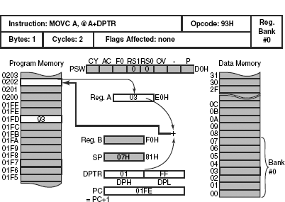
Figure 12.1 Execution of MOVC A, @A+DPTR instruction
Instruction MOVC A, @A+PC works in an identical way to get a byte from the program memory. However, in this case, the accumulator content is added with the current value of the PC. Note that at the time of this addition, the PC would be pointing to the first byte of the next instruction located immediately after MOVC instruction. This addition does not physically change the value of the PC. The value (16-bit sum) is used to copy the target byte from the program memory to the accumulator. An example case of this instruction is illustrated in Fig. 12.2. Assuming that the 1-byte MOVC instruction exists in the program memory at location 01FDH and the accumulator contains 04H, data from the program memory location 0202H would be copied to the accumulator. This 0202H is obtained by incrementing the PC to the start of the next instruction, that is 01FEH, and then adding 04H to it.

Figure 12.2 Execution of MOVC A, @A+PC instruction
MOVC instruction is useful for getting entries from look-up tables. For an appropriate use of MOVC instruction, refer to Example 12.1 of this chapter.
MOVC instruction is applicable for both internal (on-chip) as well as external program memory. However, it is not applicable for data memory of 8051.
12.3 | MOVX Instruction
MOVX instruction communicates between the accumulator and the external data memory only. There is no scope of communicating with any other type of memory (program memory or internal data memory) through this instruction. Variations of this instruction are presented in Table 12.3.
Table 12.3 Variations of MOVX instruction
| Instruction | Function |
|---|---|
| MOVX A, @Ri | Load the accumulator by a byte from the external data memory using indirect 8-bit addressing |
| MOVX A, @DPTR | Load the accumulator by a byte from the external data memory using indirect 16-bit addressing |
| MOVX @Ri, A | Store the accumulator in the external data memory using indirect 8-bit addressing |
| MOVX @DPTR, A | Store the accumulator in the external data memory using indirect 16-bit addressing |
As we may observe from Table 12.3, the accumulator is the only location that is capable of transacting data with the external data memory. It may be noted that the external data memory is addressed by the 16-bit address. Addressing architecture of the internal data memory is 8 bit. To generate this 16-bit external address, either DPTR or register R0/R1 may be used. At the time of using MOVX A, @Ri type of instruction, the lower 8 bits of the external data memory addresses are stored in R0 or R1, which is the output through port P0 in a multiplexed form with the incoming 8-bit data. To generate upper 8 bits of the external data memory address, help from another port may be asked.
As an example case, execution of the instruction MOVX A, @R0 is illustrated in Fig. 12.3. Presently, register R0 of bank #0 contains F9H, which is used as the lower byte of the 2-byte external address. It is assumed that the higher byte, namely 1FH, had already been generated through any one of the remaining three ports, P1, P2 or P3. After execution of this instruction, the accumulator would be loaded by the present content of the external data memory location 1FF9H. No flags would be affected, and the content of register R0 would remain unchanged.
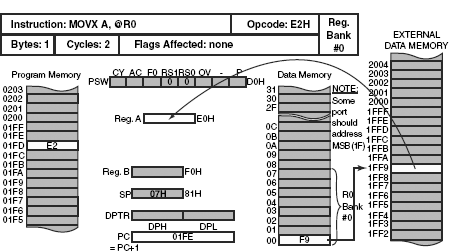
Figure 12.3 Execution of MOVX A, @R0 instruction
An identical effect may be achieved by MOVX A, @DPTR instruction as illustrated in Fig. 12.4. In this case, the complete 16-bit address 1FF9H must be stored within DPTR before the execution of the instruction. This is emitted through ports P0 (lower byte) and P2 (higher byte) and the target data from the external data memory that is copied to the accumulator. No flags are affected, and the DPTR remains unchanged. There is no need, in this case, to entrust any port to output any of the address bytes.

Figure 12.4 Execution of MOVX A, @DPTR instruction
To store data from the accumulator to the external data memory, MOVX, @Ri, A instruction may be used. As an example case, an illustration of the execution of the MOVX @R1, A instruction is presented in Fig. 12.5. In this case, R1 has the lower byte of the 16-bit address (F9H), and the higher byte is assumed to be the output through any other port except port P0. After the execution of the instruction, the accumulator content is copied to the external data memory location. No flags are affected, and the content of the register R1 remains unchanged.

Figure 12.5 Execution of MOVX @R1, A instruction
DPTR may also be used for storing the accumulator content in the external data memory as illustrated in Fig. 12.6. The complete 16-bit address must be available in the DPTR before the execution of this instruction. Just like the previous case of MOVX A, @DPTR, here also, ports P0 and P2 would be used to hold the 16-bit address for the external data memory till the data byte transaction is complete. Port P0 would also transmit the 8-bit data from the accumulator to the external location by multiplexing. No flags would be affected, and the original content of the DPTR would remain unchanged.

Figure 12.6 Execution of MOVX @DPTR, A instruction
To conclude the discussions about communication between the external data memory and the accumulator, it may be pointed out that the operation becomes more straightforward when the DPTR is used. However, DPTR may only be incremented and cannot be decremented by 16-bit. On the other hand, usage of R0 or R1 would demand a prior use of another port other than P0 to hold the higher byte of the 16-bit address. However, in this case, the registers offer both incrementing and decrementing features, which might be appropriate for some data transactions within a limit of 256 bytes. Otherwise, both types of instructions need two cycles, and both are 1-byte instructions.
Note that data flow in MOVX instruction may be of two types: either loading or storing. However, MOVC allows only loading option.
12.4 | XCH Instruction
The XCH instruction interchanges the byte variables between the accumulator and any other location. Three addressing modes available for this instruction are presented in Table 12.4. As indicated in this table, the possible addressing modes are: register direct, direct and register indirect. The details of each instruction are as follows.
Table 12.4 Addressing modes of XCH instruction
| Instruction | Addressing mode | Function |
|---|---|---|
| XCH A, Rn | Register direct | Interchange the accumulator and the registercontents |
| XCH A, direct | Direct | Interchange the accumulator and the direct address contents |
| XCH A, @Ri | Register indirect | Interchange the accumulator and the indirectly addressed contents |
As an example the execution of XCH A, R4 instruction is presented in Fig. 12.7. Assuming that bank #0 is currently selected, register R4 of bank #0 and the accumulator would interchange their contents when the instruction is executed. No flags would be affected, and the execution would take only one cycle to complete this 1-byte transaction.
Any directly addressed location’s content may also be interchanged with the accumulator using XCH A, direct instruction. As an example, direct address of 30H is used in the instruction XCH A, 30H, the execution of which is illustrated in Fig. 12.8. This is a 2-byte instruction, and the second byte of the opcode contains the direct address. The interchanging operation takes one cycle, and no flags are affected. If any port is addressed, then the data would be taken from its input pins and not from its output latches.

Figure 12.7 Execution of XCH A, R4 instruction

Figure 12.8 Execution of XCH A, 30H instruction
An example of indirect addressing ofXCH instruction is presented in Fig. 12.9. The XCH A, @R1 instruction is shown here. Assuming that register bank #0 is selected and register R1 of this bank contains 30H, the illustration shows the interchange of data between the data memory location 30H and the accumulator, which takes only one cycle without affecting any flag.

Figure 12.9 Execution of XCH A, @R1 instruction
Remember the bubble sorting technique of the previous chapter? Try to modify the program by using this XCH instruction.
12.5 | XCHD Instruction
Interchanging of only the lower nibble instead of a byte variable may be accomplished by the instruction XCHD A, @Ri, which allows only register indirect addressing mode. Assuming that bank #0 is selected and register R0 contains 30H, execution of instruction XCHD A, @R0 is illustrated through Fig. 12.10. The exchange takes place between bits 3 and 0 of the accumulator and the indirectly addressed location 30H. No flags are affected.
As an example case, if the accumulator contains 3BH and location 30H contains 25H, then after the execution ofXCHD A, @R0 instruction would leave 35H in the accumulator and 2BH in location 30H. Note that the respective higher nibble remains unchanged. This instruction is mostly used for the BCD number manipulations.
12.6 | MUL Instruction
MCS-51 offers single-byte opcode for multiplying operation, which takes four cycles. Multiplication of two unsigned integers, located within the accumulator and B register, is performed, and the 16-bit result is made available in the accumulator and B register. Note that no other registers may be used for this operation. The lower byte of the product is available in the accumulator, and its higher byte is placed in B register. The CY flag is always cleared by this instruction. If the product is greater than FFH (255d), then the OV flag is set; otherwise it is cleared. No other flag would be changed.
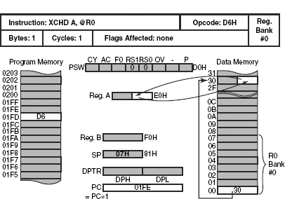
Figure 12.10 Execution of XCHD A, @R0 instruction
As an example case, the execution of MUL AB instruction is illustrated in Fig. 12.11. It is assumed that the original content of the accumulator, before execution of the instruction, was 04H. Register B contained 08H before multiplication. After execution of the MUL AB instruction, the product 20H (32d) would be available in the accumulator and register B would contain 00H. As the product is not more than FFH, OV flag would be cleared. As indicated before, CY flag would always be cleared. No other flags would be affected.
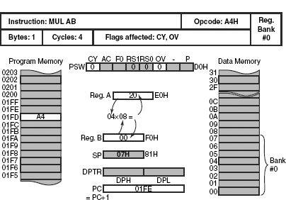
Figure 12.11 Execution of MUL AB instruction
It is a good practice to check the OV flag of PSW before using the result of any MUL instruction. If OV is set, do not forget to use the upper byte of the result available in register B.
12.7 | DIV Instruction
Allowing the DIV AB instruction, MCS-51 offers the scope of dividing an unsigned integer by another unsigned integer, both of an 8-bit value. The integer in the accumulator is divided by the integer in register B. The quotient is available, after execution, in the accumulator, and the remainder may be found in register B. Both CY and OV flags are cleared. No other flags are affected. If it becomes a case of division by zero (register B containing zero before execution), then the OV flag would be set thus indicating the division by zero error. In such a case, the accumulator and register B contents would be undefined.
As an example case, Fig. 12.12 shows the execution of DIV AB instruction assuming that the accumulator contained 21H (33d) and register B contained 10H (16d) before the execution of DIV AB instruction. As illustrated, after the execution of the instruction, the accumulator would contain 02H and register B would be having 01H, indicating the quotient and the remainder, respectively. Both CY and OV flags would be cleared without affecting any other flags.

Figure 12.12 Execution of DIV AB instruction
12.8 | DA A Instruction
To perform BCD arithmetic, MCS-51 offers DA A instruction. Execution of this instruction needs some prerequisites. To start with, DA A may only be used immediately after executing either ADD or ADDC instruction of any addressing mode. DA A would be of no use even after a SUBB instruction. Loading any number in the accumulator and then executing DA A instruction would not change the accumulator contents to its BCD equivalent (refer to Fig. 12.13).

Figure 12.13 Scope of DA A instruction
Secondly, if only BCD operands are used prior to ADD or ADDC instruction, then and then only would DA A generate correct results. This needs some clarification. If we load the accumulator by 3B, then obviously it is a hexadecimal number. However, if we load the accumulator by 32, then it may be interpreted either as a BCD or as a hexadecimal number. As already indicated, DA A instruction is applicable only with BCD arithmetic addition, and 32 would be interpreted as a BCD number in this case.
DA A is a 1-byte, one-cycle instruction with the opcode D4H (Fig. 12.14). If after any addition of BCD numbers any BCD digit within the accumulator is changed to a non-BCD value, then the execution of this instruction would change it back to its correct BCD value. If the digits are within their BCD limits, the accumulator would remain unchanged. In essence, the DA A instruction adds any one of 00, 06, 60 or 66 with the accumulator, depending upon the content of the accumulator and PSW register. These conditions are illustrated in Fig. 12.15.

Figure 12.14 Execution of DA A instruction
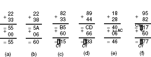
Figure 12.15 Different conditions of executions of DA A instruction
Fig. 12.15 presents six different conditions where DA A instruction may be executed. Note that in all cases two two-digit BCD numbers are added, and immediately after this addition, DA A instruction is executed. In the first case [Fig. 12.15(a)], the result of the initial addition was 55 without any carry or auxiliary carry. Therefore, DA A adds 00 with the sum to produce the unaltered result of 55 in the BCD.
The second one is the case of adding BCD numbers 22 with 38, which results in a sum of 5A in the accumulator. The execution of DA A instruction in this case would add 06 with the sum, as the LS digit of the sum is more than 9 [Fig. 12.15(b)]. This produces a result of 60, which is the correct BCD representation of the sum of 22 and 38, both being BCD.
The third case [Fig. 12.15(c)] shows that MSB (B) of the sum B5 invited the DA A instruction to add 60 with the sum to generate the result of 115. Note that in this case, CY is set, indicating that the result of the BCD addition is more than 99 in the BCD.
In the fourth case [Fig. 12.15(d)], the sum becomes CD, and DA A must add 66 with this to generate the correct result of 133, again indicating a carry. These first four cases show that if any digit exceeds 9, then 6 must be added with that digit during DA A execution.
However, in the fifth case, addition of 18 and 28 (both BCD numbers) produce 40 [Fig. 12.15(e)], and neither 4 nor 0 is more than 9. Then why is DA A adding 06 with it? Because there is a carry from bit 3 to bit 4 during this addition, as indicated by the AC flag. That is the reason for adding 06 to get the correct result of 46.
In the last case, addition of 95 and 82 generates 117 with the carry set. Therefore, although none of the digits is more than 9, 60 is then added with the accumulator by the DA A instruction to indicate the correct BCD result of 177. Note that CY remains set and unchanged in this case.
Therefore, to summarize the discussions on DA A:
- DA A instruction is applicable only after execution of ADD or ADDC instruction.
- This addition must be performed with BCD numbers without using any hexadecimal number.
- During this addition, if AC is set or CY is set or any digit exceeds 9, then DA A would take appropriate action to change the result to correct BCD representation.
- If CY is set even after the execution of DA A instruction, then it indicates that the result is more than 99 in BCD.
DA A instruction is applicable only for the accumulator.
12.9 | JMP Instruction
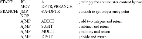
JMP @A+DPTR instruction adds the content of the accumulator, taking it as an unsigned integer, to the content of the DPTR to generate a 16-bit result, which is loaded in the PC to fetch the next instruction from that location. Neither the previous content of the accumulator or DPTR is changed, nor is any flag affected. This 1-byte instruction takes two cycles to be executed, which is illustrated in Fig. 12.16. Assuming that the DPTR contains 0200H and the accumulator contains 01H, control would branch unconditionally to the location 0201H after the execution of this instruction. This instruction is widely used to perform branching operations such as ‘case’ statements in high level languages (refer to solved Example 12.2).
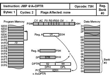
Figure 12.16 Execution of JMP @A+DPTR instruction
12.10 | SWAP Instruction
The execution of SWAP A instruction is illustrated in Fig. 12.17. This 1-byte, one-cycle instruction interchanges the content of the upper and the lower nibbles of the accumulator. No flags are affected. Considering as an example, if the accumulator originally contained 2FH, the accumulator would contain F2H after execution of the SWAP A instruction without affecting any flags. This instruction is equivalent to four successive RR A or RL A instructions.
SWAP is applicable only for the accumulator and not for any other register or memory location.

Figure 12.17 Execution of SWAP A instruction
12.11 | JBC Instruction
The 3-byte, two-cycle instruction JBC (opcode 10H) is identical with the JB instruction in all respects, except that it clears the addressed bit before jumping to the relative address if the addressed bit is set. Otherwise, it proceeds sequentially if the addressed bit is 0 (cleared). It does not affect any flag of PSW. The second byte contains the address of the bit, and the third byte contains the relative offset for jumping, having the range of 127 bytes forward or 128 bytes backward.
12.12 | RETI Instruction
The 1-byte, two-cycle (opcode 32H) instruction RETI (return from interrupt service routine) is identical with the instruction RET (return from subroutine) in all aspects except one. RETI enables the disabled interrupt. Whenever any interrupt is acknowledged and the control branches to its service routine, that particular interrupt is automatically disabled for the time being by the processor itself so that multiple false interrupt branching do not take place. However, the concerned interrupt would not function properly against fresh interrupt requests unless it is enabled again before returning from that interrupt’s service routine. This is done by RETI, which should be placed at the end of any interrupt service routine. RETI does not affect any flag of the PSW.
12.13 | Solved Examples
Example 12.1
Purpose: Application of MOVC instruction in table look-up method.
Problem
Register R4 would be loaded by an unsigned integer, which may vary from 0 to 5. Find the square of the integer and store it in R5.
Solution
Using MOVC instruction and a table of squares, the problem may be solved in the following way:
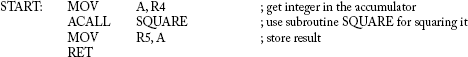
; Subroutine SQUARE with its table SQTAB.
; This table must be located immediately after the subroutine.

The INC A instruction in subroutine SQUARE is not required if the range of the input started from 1 and not from 0.
Example 12.2
Purpose: Application of the JMP instruction.
Problem
Write a program to perform addition, subtraction, multiplication or division as per accumulator content of 1, 2, 3 or 4, respectively. Assume that two related operands are available in R2 and R3.
Solution
This program may be developed with DJNZ acc, rel instruction also. However, using JMP @A+DPTR makes the program compact and more efficient. This is more so when the range of the offset is larger.
The first instruction doubles the accumulator content. This is necessary to get the proper entry point using AJMP instruction. Note that AJMP instruction takes 2 bytes. The second instruction loads DPTR with the address of the program memory location indicated by the label ‘BRANCH’. The third instruction gets the next executable instruction’s address, also known as ‘branching address’, by adding DPTR to the accumulator content while taking both as unsigned integers. Because JMP is a 1-byte instruction, an NOP instruction is placed to maintain a gap of 2 bytes.
Depending upon the original content of the accumulator, one of the four AJMP instructions would be performed to get the entry point to the relevant subroutine.
; Subroutine to perform addition.
| ADDIT: | MOV | A, R2 |
| ADD | A, R3 | |
| RET |
; Subroutine to subtract one register content from the other.
| SUBIT: | MOV | A, R2 |
| CLR | C | |
| SUBB | A, R3 | |
| RET |
; Subroutine to perform multiplication of two unsigned integers.
| MULIT: | MOV | A, R2 |
| MOV | B, R3 | |
| MUL | AB | |
| RET |
; Subroutine to perform unsigned integer division.
| DIVIT: | MOV | A, R2 |
| MOV | B, R3 | |
| DIV | AB | |
| RET |
Example 12.3
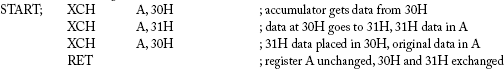
Purpose: Application of XCH instruction.
Problem
Write a program to interchange data between data memory locations 30H and 31H.
Solution
This may be performed in various ways, and one of them may be as follows. The original content of the accumulator remains unchanged.
We shall discuss a few more examples of application of some of these instructions in the next chapter.
SUMMARY
Instructions such as MOVC, MOVX, XCH, MUL, DIV and DA A were discussed in this chapter. These are very powerful instructions to perform BCD arithmetic, unsigned integer multiplication and division, to communicate with external data memory, to get a constant from the program memory.
POINTS TO REMEMBER
- DA A is applicable after ADD or ADDC instructions only if its operands are already in BCD.
- After execution of MUL AB instruction, the lower byte of the 16-bit product would be available in the accumulator and the higher byte in the B register.
REVIEW QUESTIONS
Evaluate Yourself
- Which of the following instructions, when executed four times, would perform the same duty as of the SWAP A instruction?
- RLC A
- RR A
- RRC A
- None of these
- Communication with the external data memory may be achieved only through
- The accumulator
- B register
- PSW
- None of these
- How many addressing modes are offered by XCHD instruction?
- One
- Two
- Three
- None of these
- After execution of MUL AB instruction, the higher byte of the product would be available in
- The accumulator
- B register
- PSW
- None of these
- After execution of DIV AB instruction, the quotient is available in
- The accumulator
- B register
- PSW
- None of these
- DA A instruction is applicable only for the following number type?
- Binary
- Hexadecimal
- BCD
- None of these
- DA A instruction may be used immediately after the execution of
- SUBB
- MUL
- DIV
- None of these
- The instruction JMP @A+DPTR is capable of transferring the control within
- 256 bytes
- 2K bytes
- 64K bytes
- None of these
- The base address of MOVC A, @A+PC instruction is
- PC
- PC+1
- PC+1+A
- None of these
- The base address of MOVC A, @A+DPTR instruction is
- DPTR
- DPTR+1
- DPTR+1+A
- None of these
Search for Answers
- Which addressing mode is used by MOVX instruction?
- How is the 16-bit address generated during execution of MOVX A, @Ri instruction?
- What is the difference between XCH and XCHD instructions?
- Is it possible to exchange a byte between R2 and R4 of the current register bank, using XCH instruction?
- What would happen if you tried to divide a number by zero, using DIV AB instruction?
- How many flags are affected by DA A instruction?
- What are the restrictions in using DA A instruction?
- How does DA A instruction indicate that the result is more than 99 in BCD?
- Is it possible to perform a backward jump using JMP @A+DPTR instruction?
- What changes would be necessary in Example 12.1 to get the cube of the integer input?
Think and Solve
- How can Example 12.3 be modified so that data in 30H is shifted to 31H, data in 31H is shifted to 32H and data in 32H is shifted to 30H?
- What is the limitation of the size of the table that may be looked up using MOVC A, @A+PC instruction?
- During the usage of MOVX A, @DPTR instruction, would the higher byte of the 16-bit external data memory address be latched in P2 so that the subsequent MOVX A, @Ri instruction is sufficient to get the correct data in the accumulator?
- What would be the branching address if the accumulator contains 00H during the execution of JMP @A+DPTR instruction?
- How can an infinite loop be generated using JMP @A+DPTR instruction?
- In Example 12.2, what changes would be necessary if all AJMP instructions are replaced by LJMP instructions?
- Is it possible to multiply a 16-bit unsigned integer by an 8-bit unsigned integer using MUL instruction? Justify your answer.
- Assume there is a display of a digital clock in BCD format with a range of 12 h. Write a program that can be called at every minute to change its hour and minute counters, which are also BCD counters.
- Write a program to copy 16 bytes of data from the external data memory location 2000H onwards to internal data memory location 30H. Assume that port 1 is interfaced with the higher 8-bit address of the external data memory.
- Sixteen-bit values of the square of integers are stored in a table that starts from program memory location 0200H onwards. The lower byte of the 16-bit number is at the lower address, and the higher byte is at the higher address. Assuming that the accumulator contains the integer whose square is required, write a routine to get the result using table look-up procedure (MOVC instruction).