26
ADVANCED MICROCONTROLLERS
CHAPTER OBJECTIVES
In this chapter, the reader is introduced to a few advanced microcontrollers. After completion of the chapter, the reader should be able to understand some of the features of:
- 8-bit microcontroller: Atmel's AVR (Atmega8),
- 16-bit microcontroller: Intel's MCS-96 and
- 32-bit microcontroller: ARM microcontrollers
26.1 | Introduction
After commercial introduction of microcontrollers in the world market, system designers and developers started realizing that it would provide a cost-effective solution to various programmable digital systems in contrast to the systems designed with microprocessors. This rise of demand of microcontrollers has led to the introduction of many varieties of microcontrollers in the IC market. Today, against every microprocessor-based system, there are at least 20 microcontroller-based systems, which may even increase to as many as 50 in the near future as visualized by the experts. Out of these, we will have some brief discussions on three advanced microcontrollers, which have been developed after 8051. However, the information presented in subsequent sections is introductory in nature, and interested readers may consult the relevant manufacturer's datasheets for detailed features, accurate specifications and functioning.
Are these microcontrollers going to completely replace all microprocessors in near future? Till date, the answer is 'no'. Microprocessors have their own advantages also. They are more suitable for a larger system, without any power consumption restrictions. However, who knows what is stored as the future of microprocessors?
26.2 | AVR Microcontrollers
AVR series microcontrollers were developed by Atmel around 1996. Atmel has been the pioneer in introducing Flash memory for program storage, available in AVR. These advanced RISC microcontrollers are built around the Harvard architecture. Two popular versions of these microcontrollers are ATmega8 and ATmega16. TINY and XMEGA versions of AVR are also available to cater to various application demands. In this section, we will take a closer look at ATmega8, and finally, we will identify the differences in ATmega16 against it.
26.2.1 | Important Features
The following are some of the important features of ATmega8.
- 8-bit advanced RISC architecture
- Register-to-register architecture without any accumulator
- 130 instructions including signed and unsigned multiplication
- 32 general-purpose 8-bit registers, all capable of storing the result
- Fully static to 16 MHz operational frequency
- 8K bytes on-chip Flash program memory
- 1K bytes on-chip SRAM for data storage
- 512 bytes on-chip EEPROM
- Programming lock for software security
- 23 programmable I/O lines
- Two 8-bit and one 16-bit Timer/Counters.
- 6 channel 10-bit on-chip ADC (8 channel for TQFP package)
- Programmable serial USART
- SPI serial interface
- Watchdog Timer with separate on-chip oscillator
- On-chip analog comparator
- External and internal interrupt sources
- Five sleep modes for power management
Register to register architecture is a feature which totally eliminates the need of any accumulator. In early days of processors, all results were available in the accumulator only. Later the situation improved making any register to hold the result. In 8051, we got a glimpse of it when we observe that results of some logical operations with bytes are also available in some directly addressed memory locations.

Figure 26.1 Pins and signals of ATmega8 (28-pin PDIP)
26.2.2 | Pins and Signals
Fig. 26.1 shows all signals against their respective pin numbers for a 28-pin PDIP of ATmega8. Note that all 23 I/O lines have alternative functions. Only five input lines, reserved for power supply, are not assigned any alternative functions.
Observe that this 28-pin device (ATmega8) offers more features than a standard 40-pin 8051.
26.2.3 | External Reset and Crystal Inputs (Optional)
An initial observation of Fig. 26.1 would reveal that even the system reset input or external crystal inputs are optional. This is because the device contains a built-in RC oscillator circuit capable of generating any one of the four standard software-selectable frequencies of 1.0, 2.0, 4.0 and 8.0 MHz. Alternatetively, an external crystal may also be connected with Pins 9 and 10 for any desired frequency up to 16 MHz (8 MHz for ATmega8L). There is an internal power-on reset facility to initialize various parameters in absence of any external reset input, which is optional.
26.2.4 | Operating Voltages and Power Consumption
As most of the embedded systems designed with microcontrollers are battery-powered, power supply and its consumption play an important role in all advanced microcontrollers. Operating voltage of ATmega8 is from 4.5 V to 5.5 V, while that of ATmega8L is between 2.7 V and 5.5 V. For an operational speed of 4 MHz with 3 V power source, it consumes 3.6 mA when it is active; this is reduced to 1 mA in its idle mode and further reduced to 0.5 μA in power-down mode. Each port pin of ATmega8L is capable of sourcing or sinking 20 mA of current at 5 V and 10 mA of current at 3 V. Note that the sourcing and sinking limits are identical for this device.
26.2.5 | Internal Architecture
A simplified internal architecture of ATmega8 is presented in Fig. 26.2. As it may be readily observed, its central feature is the AVR core (the portion not shaded), which consists ALU, 32 general-purpose registers including three index registers, the processor status register or flag register (SREG), program counter (PC), stack pointer and the instruction register with the instruction decoder generating various control lines.
The remaining portion contains program and data memory (Flash, SRAM and EEPROM), ADC with multiplexing unit, I/O ports (designated as B, C and D), Timer/Counters, USART, Interrupt unit, analog comparator interface, oscillator circuits and serial interfaces. The reader should note the absence of any external memory interfacing provision in AVR. The AVR works on the principle that for larger memory demand, some other AVR version needs to be selected.
26.2.6 | Program Memory (Flash)
As all instructions’ opcodes for ATmega8 are either 16-bit or 32-bit in length, the on-chip 8K bytes of program memory are arranged as 4K words, which are accessed by a 12-bit PC. For software security, the Flash is divided into two sections, namely, Boot section and Application Program section. The Boot section occupies the higher part of the Flash and the lower portion is left for application programs as shown in Fig. 26.3. Note that the size of the Boot section is configurable through fuses.

Figure 26.2 Simplified internal architecture of Atmega8
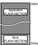
Figure 26.3 Map of program memory (Flash)
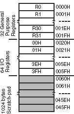
Figure 26.4 Organization of 1,120 bytes of SRAM data memory
26.2.7 | Data Memory (SRAM)
ATmega8 offers 1,120 bytes of data memory (SRAM), which is divided into three parts, as illustrated in Fig. 26.4. The lowest 32 bytes are occupied by 32 general-purpose registers designated as R0, R1 and so on upto R31. Register pairs from R26 to R31 are also designated as three index registers, X, Y and Z. Registers may be addressed by their names (R0, R1, etc.) or by direct or other types of addressing modes. Direct addresses of registers vary from 0000H to 001FH
ATmega8 does not have any accumulator for storing the result of arithmetical or logical operations. The destination register indicated in the opcode of the instruction holds the result. This is known as 'register-to-register architecture'. It would be the designated register pair that holds the 16-bit results. Any one or a pair of 32 general-purpose registers may be used as the destination register.
Sixty-four I/O registers are located after general-purpose registers. In 8051, we have come across Special Function Registers or SFRs. In ATmega8, these I/O registers serve the identical purpose as that of SFRs for controlling various activities of processor operations. Note that two types of addresses are applicable for I/O registers: absolute address (from 0020H to 005FH) and I/O register address (from 00H to 3FH). The remaining 1,024 bytes of SRAM may be used as a scratch pad for data storage.
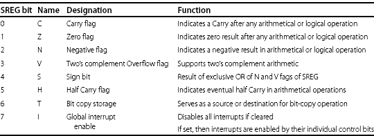
26.2.8 | Status Register
Located as the highest addressed register of I/O registers (absolute address 005FH), this 8-bit register contains eight flags as shown in Fig. 26.5. Table 26.1 presents the names of these flags along with their functions.
26.2.9 | Stack and Stack Pointer
ATmega8 allows stack anywhere within 1,024 bytes of data SRAM. The stack must avoid the lower 96 bytes of SRAM area containing general-purpose registers and I/O registers. Stack is always pointed by the 16-bit stack pointer, which is composed of two 8-bit registers SPH and SPL. Note that a PUSH command decreases the stack pointer and a POP command increases it. That is, the stack grows from higher to lower address, and the highest assigned address of the stack area is to be used to initialize the stack pointer. For example, if 0100H to 01FFH of SRAM is earmarked for stack, then the stack pointer must be initialized by 01FFH with SPH containing 01H and SPL containing FFH. To store the return address for subroutine calls, the SP uses a post-decrement addressing scheme.
Figure 26.5 Details of SREG of ATmega8
Table 26.1 Descriptions of ATmega8 flags
26.2.10 | Power Management and Sleep Modes
ATmega8 offers five sleep modes for efficient power management. They are
- Idle mode
- ADC noise reduction mode
- Power-down mode
- Power-save mode
- Standby mode
The SLEEP instruction must be executed with MSB of MCUCR register set and proper sleep mode selected through SM2, SM1 and SM0 bits of MCUCR. A reset or interrupt wakes up the CPU, and after the start-up time and an additional four cycles of halting, the processor starts executing from the next instruction after the SLEEP instruction if it is awakened by interrupts. If it is awakened by reset, then the execution starts from the reset vector.
Compare these power saving modes with those offered by 8051.
26.2.11 | System Reset
ATmega8 offers four sources for generating a system reset signal. Table 26.2 indicates these sources with a brief description. During reset, all I/O registers are initialized by their reset values and the program starts executing from the reset vector. The source for generating the reset is available after every reset in the least significant 4 bits of the MCUCSR register.
Table 26.2 Reset sources for ATmega8
| Reset type | Executed when |
|---|---|
| Power-on reset | The supply voltage is below the power-on reset threshold |
| External reset | A low-level is applied at external RESET input for longer that the minimum pulse length |
| Watchdog reset | Watchdog is enabled, and the Watchdog Timer period expires |
| Brown-out reset | The supply voltage is below the brown-out reset threshold, and brown-out detector is enabled |
26.2.12 | Watchdog Timer
Any Timer generates an interrupt at its terminal count, and Watchdog Timer is no exception. However, the specialty of the Watchdog Timer is that instead of generating a normal interrupt and drawing the attention of the processor, it triggers a system reset. This is very useful if the system is in an infinite loop or just 'hanging'. To avoid any unwanted system reset, the Watchdog Timer must be periodically serviced by the system software.
ATmega8 offers a built-in Watchdog Timer, which may be enabled or disabled by the software commands through its register, which is designated as WDTCR. The Watchdog Timer is operated by a separate internal oscillator at 1 MHz frequency.
26.2.13 | ATmega8 Instruction Set
ATmega8 has a rich set of 130 instructions. They are divided into five groups, namely
- Arithmetical and logical instructions,
- Branch instructions,
- Data transfer instructions,
- Bit and bit-test instructions and
- MCU control instructions.
Group-wise descriptions of all instructions are presented from Table 26.3 to Table 26.7 along with some brief introductory comments.
Arithmetical and logical instructions: All conventional arithmetical (like add, subtract, etc.) and logical (like AND, OR, XOR, etc.) along with increment by one and decrement by one instructions are available in this instruction group. In general, these instructions deal with 8-bit operations. Both unsigned and signed multiplication instructions are available for 8-bit numbers, including fractional format, producing 16-bit result. Table 26.3 presents a summary of all arithmetical and logical instructions offered in ATmega8.
Branch instructions: Program branching plays an important role for any software, and a wide variety of branching instructions is offered in ATmega8 as presented in Table 26.4. Branching instructions dependent on SREG flag bits are related with PC within the range between −63 and +64 bytes. The Z register (16-bit) plays an important role in some jump and call instructions by providing the 16-bit branching address to be loaded in PC.
Data-transfer instructions: A large number of data transfer instructions are available in ATmega8 with several addressing modes. Some instructions offer post-increment or pre-decrement options through index registers for easier access to arrays. In case of the post-increment option, the data is first copied from the address available in the index register and then the index register content is incremented by one. On the other hand, for the pre-decrement instructions, the content of the index register is first decremented by one and then the data pointed by it is copied to the destination register.
Table 26.3 ATmega8 Arithmetical and logical instructions

Table 26.4 ATmega8 branch instructions

Table 26.5 ATmega8 data transfer instructions
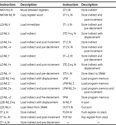
This post-increment and pre-decrement operations are always limited to 256 bytes as only the lower part of the 16-bit register is changed. Table 26.5 presents the summary of all data transfer instructions offered by ATmega8.
Bit and bit-test instructions: ATmega8 allows transactions of bit-wise information for all 32 general-purpose registers and lower 32 I/O registers. Bits of upper 32 I/O registers cannot be accessed in this fashion. The source or destination of the bit-information transfer must be the T flag bit of SREG, the status register. Bits are identified by their respective register's name and the concerned bit number (0 to 7).
Bit-oriented instructions allow the setting and clearing of all flag bits of SREG and other addressable bits of general-purpose registers and I/O registers. Instruction for swapping 4 bits (nibble) at a time is also offered and is applicable for all 32 general-purpose registers. Table 26.6 presents a summary of these instructions.
MCU control instructions: Out of three instructions of this group (shown in Table 26.7), SLEEP allows power management as discussed earlier. The Watchdog Timer may be reset by the WDR instruction.
Table 26.6 ATmega8 bit and bit-test instructions
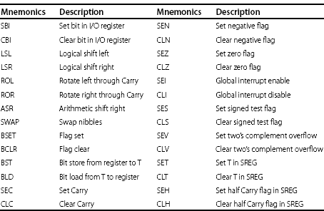
Table 26.7 ATmega8 MCU control instructions
| Mnemonic | Description |
|---|---|
| NOP | No operation |
| SLEEP | Sleep |
| WDR | Watchdog reset |
26.2.14 | Comparison Between ATmega8 and ATmega16
An advanced version of ATmega8 is ATmega16, which offers more program memory and I/O lines. Available in a 40-pin PDIP (also in other packages), ATmega16 offers all instructions available in ATmega8 (plus one extra) and allows Joint Test Action Group (JTAG) interface for debugging, which is explained in the next section.
It also offers one extra PWM channel as compared with ATmega8 and one more sleep mode for better power management. The major differences between ATmega8 and ATmega16 are presented in Table 26.8. For more details about ATmega8 and ATmega16, interested readers may consult the manufacturer's datasheets.
Table 26.8 Differences between ATmega8 and ATmega16
| ATmega8 | ATmega16 | |
|---|---|---|
| Number of instructions | 130 | 131 |
| Size of program memory (Flash) | 8K | 16K |
| Number of I/O lines | 23 | 32 |
| PDIP | 28-pin | 40-pin |
| PWM channels | 3 | 4 |
| Sleep modes | 5 | 6 |
| JTAG interface | Not available | Available |
26.2.15 | JTAG Interface
JTAG is a special 4/5-signal interface to test functional characteristics of any circuit board or chip. Originally designed to test circuit boards, JTAG has now been accepted as the IEEE 1149.1 standard and is known as Standard Test Access Port and Boundary-Scan Architecture. Presently JTAG is extensively used for IC testing.
Generally, JTAG connectors are 10-pin or 20-pin and all pins of one side are connected with GND. Any JTAG port of a device offers the following signals.
- TCK (test clock)
- TMS (test mode select)
- TDI (test data in)
- TDO (test data out)
- TRST (test reset) [optional]
With only one data line available, JTAG adopted serial protocol for testing. Multiple devices with JTAG port may be daisy chained for purpose of testing.
26.3 | MCS-96 Microcontrollers
MCS-96 represents a family of 16-bit microcontrollers launched by Intel during 1982. It is often referred to as the 8XC196 family or simply 80196. It is widely used in printers, modems and hard-disk drives. These microcontrollers have different operating frequencies and are offered in various packages. For the purpose of initial understanding, we take 8XC196 as a sample member of this family of MCS-96 microcontrollers.
26.3.1 | Important Features
The following are some of the important features of 8XC196.
- Register-to-register architecture
- 16K on-chip ROM/OTPROM
- 488 bytes register RAM
- Five 8-bit I/O ports
- High speed I/O subsystem
- Full-Duplex serial port
- 16-bit multiply and divide instructions
- 8 or 10-bit A/D converter with sample and hold
- Four 16-bit software Timers
- 16-bit up/down Counter with capture
- Dynamically configurable 16-bit or 8-bit bus-width
- Three PWM outputs
- 16-bit Watchdog Timer
- 28 interrupt sources, 16 vectors
 bus protocol
- Power-down and idle modes
26.3.2 | Pins and Signals
Fig. 26.6 illustrates pin and signal details of 8XC196 as in a 68-pin PLCC. Note that it is also available in 80-pin QFP and 80-pin SQFP. A brief introduction of all major signals is given in Table 26.9. Apart from ton-chip memory, MCS-96 offers the scope for interfacing external memory, if required, for the system. Complete 16-bit address and data lines along with necessary control signals are available for this interfacing.
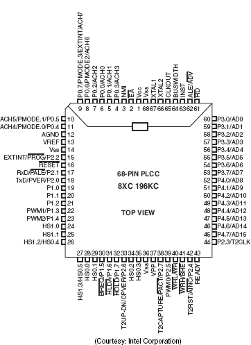
Figure 26.6 Pins and signals of 8XC196 (68-pin PLCC)
26.3.3 | Internal Architecture
MCS-96 offers a special interface for high-speed I/O devices. HS0 and HS1 pins are reserved for this operation. Out of five ports, one port (Port 0) is an input-only port and others are bi-directional. Port 0 is meant to be used for analog input for ADC channels. Otherwise it can also receive digital inputs.
Various other features are available in MCS-96, some of which are presented in the simplified internal architecture diagram in Fig. 26.7. The most important feature ofMCS-96 is its register-to-register architecture. This avoids the conventional accumulator to store the result of all ALU operations. In MCS-96, any register can serve the purpose of the accumulator, and the ALU is for the register set; that is the reason for designating it as RALU. This architecture improves the I/O operation speed, as any register content may directly be moved out through the port or received without the need of passing it through an accumulator.
MCS-96 decodes the instructions through micro-coding, as indicated in Fig. 26.7. This micro-coding engine along with RALU, 24 bytes CPU SFR and 488 bytes of register RAM complete the CPU of the device or its core. The system bus width is programmable as either 8-bit or 16-bit through the BUSWIDTH input pin and the programmable condition of the CCR bit.
Table 26.9 Signal description of 8XC196
| Signal | Description/Function |
|---|---|
| Vcc | Main supply voltage (5V). |
| Vss | Digital circuit ground (0V). There are multiple Vss pins, all of which must be connected. |
| VREF | Reference voltage for ADC (5V). It is also the supply voltage to the analog portion of ADC and the logic used to read Port 0. It must be connected if these are to function. |
| ANGND | Reference ground for ADC. |
| VPP | Timing pin for the return from power-down circuit. It also supplies programming voltage for the EPROM device. |
| XTAL1 | Input of the oscillator inverter and of the internal clock generator. |
| XTAL2 | Output of the oscillator inverter. |
| CLKOUT | Output of internal clock generator. Frequency is half of the oscillator frequency. |
| Active-low system reset input. | |
| BUSWIDTH | Input for bus width selection. If CCR bit is 0, bus is always 8 bit. If 1, then a high input allows 16-bit bus and a low input 8-bit bus. |
| NMI | Non-muskable interrupt input. A positive edge causes a vector through 203EH. |
| INST | Valid only for external memory accesses. It is high for instruction fetch and low for data reading. |
| Input for external memory access. | |
| Address latch enable active only during external memory access. | |
| Output only for external memory reading. | |
| Output only for external memory writing. | |
| Activated only during external memory write cycles. | |
| READY | Input to lengthen external memory cycles. |
| HSI | Inputs to high-speed input unit (HIS.2 and HIS.3). |
| HSO | Outputs from high-speed output unit (six HSO pins are available out of which two are shared). |
| Port 0 | 8-bit input-only port for analog or digital inputs. |
| Port 1 | 8-bit quasi-bi-directional I/O port. |
| Port 2 | 8-bit multi-functional port. |
| Ports 3 and 4 | 8-bit bi-directional I/O port shared with multiplexed address-data bus. |
| Input requesting control of the system bus. | |
| HOLD acknowledge output, indicating release of the bus. | |
| Bus request output for pending external memory cycle. | |
| PMODE | Selects EPROM programming mode. |
| PACT | Signal indicating programming is in progress or complete. |
| CPVER | Cumulative program output verification. |
| PALE | Falling edge indicates Ports 3 and 4 contain valid programming information. |
| PROG | Falling edge indicates Ports 3 and 4 contain valid programming data. |
| PVER | Programmed byte verification. |
| AINC | Auto address input during programming. |
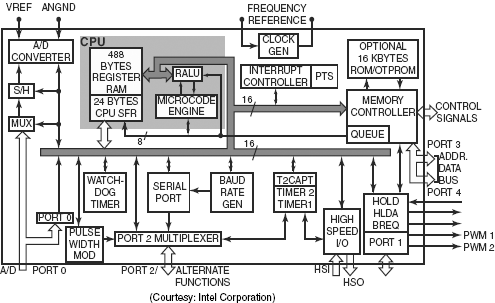
Figure 26.7 Simplified internal architecture of 8XC196
26.3.4 | Memory Map
Unlike 8051 family, MCS-96 is designed around the Princeton architecture, allowing program and data memory to share the same memory space. Total addressable memory space is 64K, which is divided in external and internal parts, as shown in Fig. 26.8. The lower address space of the memory area is reserved for internal on-chip RAM, which also accommodates SFRs and other CPU registers. Interrupts have their own vector address, which is divided in two parts, upper and lower.
26.3.5 | Addressing Modes
MCS-96 offers a rich instruction set and uses the following five addressing modes.
- Direct
- Immediate
- Indirect
- Indirect with auto-increment
- Indexed
For indirect with auto-increment addressing modes, the 16-bit target address, available in a register pair, is used to transact either 8-bit or 16-bit data, and after this data transaction, the target address, available in the register pair, is incremented by one for 8 bit and by two for 16-bit operand.
The processor offers a 0 register at address 0000H, which contains 0000H and is available for the purpose of comparison. This 0 register may also be used as a base register for indexed addressing mode, which effectively would generate a direct address anywhere within 64K memory.
26.3.6 | Instruction Set
Instructions offered for MCS-96 may be divided into 11 groups as follows.
- Arithmetical instructions
- Logical instructions

- Data transfer instructions
- Stack operations
- Jump and call instructions
- Conditional jumps
- Jump on bit conditions
- Loop control
- Single register instructions
- Shift instructions
- Special control instructions
These instructions are briefly described through Table 26.10-26.20. Interested readers should consult the manufacturer's datasheets for further details.
Table26.10 Arithmetical instructions
| Mnemonics | Brief description |
|---|---|
| ADD | Add two operands (word) |
| ADDB | Add two operands (byte) |
| ADDC | Add with Carry (word) |
| ADDCB | Add with Carry (byte) |
| SUB | Subtract (word) |
| SUBB | Subtract (byte) |
| SUBC | Subtract with Carry (word) |
| SUBCB | Subtract with Carry (byte) |
| CMP | Compare two words |
| CMPB | Compare two bytes |
| MULU | Unsigned multiply (word) |
| MULUB | Unsigned multiply (byte) |
| MUL | Multiply (word) |
| MULB | Multiply (byte) |
| DIVU | Unsigned divide (word) |
| DIVUB | Unsigned divide (byte) |
| DIV | Divide (word) |
| DIVB | Divide (byte) |
Table 26.11 Logical instructions
| Mnemonics | Brief description |
|---|---|
| AND | AND two operands (word) |
| ANDB | AND two operands (byte) |
| OR | OR two operands (word) |
| ORB | OR two operands (byte) |
| XOR | XOR two operands (word) |
| XORB | XOR two operands (byte) |
Table 26.12 Data-transfer instructions
| Mnemonics | Brief description |
|---|---|
| LD | Load a word |
| LDB | Load a byte |
| ST | Store a word |
| STB | Store a byte |
| LDBSE | Load a byte as word with sign unchanged |
| LDBZE | Load a byte as word with sign positive (0) |
| Mnemonics | Brief description |
|---|---|
| PUSH | Save on stack |
| POP | Load from stack |
| PUSHF | Save PSW on stack |
| POPF | Load PSW from stack |
Table 26.14 Jump and call instructions
| Mnemonics | Brief description |
|---|---|
| LJMP | Unconditional long jump |
| SJMP | Unconditional short jump |
| LCALL | Unconditional long call |
| SCALL | Unconditional short call |
| RET | Return from subroutine |
Table 26.15 Conditional jumps
| Mnemonics | Brief description |
|---|---|
| JC | Jump if Carry is set |
| JNC | Jump if Carry is not set |
| JH | Jump if higher |
| JNH | Jump if not higher |
| JE | Jump if equal |
| JNE | Jump if not equal |
| JV | Jump if V = 1 |
| JNV | Jump if V = 0 |
| JGE | Jump if greater or equal |
| JLT | Jump if less |
| JVT | Jump if VT = 1, clear VT |
| JNVT | Jump if VT = 0 |
| JGT | Jump if greater |
| JLE | Jump if less or equal |
| JST | Jump if ST = 1 |
| JNST | Jump if ST = 0 |
Table 26.16 Jump on bit conditions
| Mnemonics | Brief description |
|---|---|
| JBC | Jump if bit is clear |
| JBS | Jump if bit is set |
| Mnemonics | Brief description |
|---|---|
| DJNZ | Decrement and jump if not 0 |
Table 26.18 Single register instructions
| Mnemonics | Brief description |
|---|---|
| DEC | Decrement a word by 1 |
| DECB | Decrement a byte by 1 |
| NEG | Two's complement a word |
| NEGB | Two's complement a byte |
| INC | Increment a word by 1 |
| INCB | Increment a byte by 1 |
| EXT | Extract the sign of a word |
| EXTB | Extract the sign of a byte |
| NOT | Complement a word |
| NOTB | Complement a byte |
| CLR | Clear a word |
| CLRB | Clear a byte |
Table 26.19 Shift instructions
| Mnemonics | Brief description |
|---|---|
| SHL | Shift left a bit (word) |
| SHLB | Shift left a bit (byte) |
| SHLL | Shift left a bit (long word) |
| SHR | Shift right a bit (word) |
| SHRB | Shift right a bit (byte) |
| SHRL | Shift right a bit (long word) |
| SHRA | Shift right arithmetic (word) |
| SHRAB | Shift right arithmetic (byte) |
| SHRAL | Shift right arithmetic (long word) |
Table 26.20 Special control instructions
| Mnemonics | Brief description |
|---|---|
| SETC | Set Carry flag |
| CLRC | Clear Carry flag |
| CLRVT | Clear VT flag |
| DI | Disable all interrupts |
| EI | Enable all interrupts |
| NOP | No operation |
| SKIP | Skip next instruction (2 bytes) |
26.4 | ARM Microcontrollers
ARM is a 32-bit microcontroller whose core is designed by ARM Limited and is offered to other manufacturing organizations for adding necessary peripherals, fabrication and sales. Various versions of ARM are available, and it has undergone substantial changes till its inception during the early 1980s. As they are extremely efficient in power saving and operate with very low power consumption, ARM microcontrollers are widely used in modern handsets for mobile communications. ARM processors are also used in various other embedded systems, like iPODs, hand-held gaming units, disk drives and so on. Built with 32-bit architecture, ARM offers several advanced features for embedded applications.
26.4.1 | ARM Core Architecture
The success of ARM largely depended on the simplicity of its architecture. There was no micro-coding used, and this reduced the number of transistors used. A simplified schematic of the core of ARM processor is illustrated in Fig. 26.9.
One important feature in ARM architecture is its barrel shifter. This barrel shifter can perform the necessary preprocessing of register values before it enters the ALU. This allows easier calculations of wider ranges of expressions and addresses.
The register bank contains an array (file) of 32-bit registers holding signed and unsigned values. Signed 8-bit and 16-bit numbers are converted to their signed 32-bit equivalents before being loaded in these registers through hardware conversions. ARM adopts a register-to-register architecture and therefore does not contain any accumulator. The Incrementer updates the address register before the core writes or reads the next data set.

Figure 26.9 Simplified schematic of ARM processor core
26.4.2 | Versions of ARM
The design of ARM was initiated around 1983, and by 1985, the first samples, designated as ARM1, were completed. ARM2 was available in 1986. The improvement continued further, resulting in the initiation of ARM3, ARM6, ARM7, ARM9, ARM11, ARM13 and so on. As it has been already stated at the beginning of this section, ARM Limited designed only the ARM core, which was adopted with necessary peripherals by different manufacturing companies, like Atmel, Samsung and Philips. This has created a very large family of ARM processors with a substantial number of versions.
26.4.3 | Important Features
The complexity of the ARM processor may easily be understood if we glance through its basic features. Out of a very wide variety of ARM processor models, we will take a look at Samsung's S3C4510B, which is fabricated around ARM7TDMI core. Some of the important features of this processor are as follows.
Package type
- 208-pin QFP
Operating frequency
- Up to 50 MHz
Operating voltage
- 3.3V +/- 5%
Architecture
- Fully 16/32-bit RISC architecture
- Integrated system for embedded ethernet applications
- Cost-effective JTAG-based debug solution
System manager
- 8/16/32-bit external bus support for ROM/SRAM, Flash memory, DRAM and external I/O
- One external bus master with bus request/acknowledge pins
- Programmable access cycle (0-7 wait cycles)
- Four-word depth write buffer
- Cost-effective memory-to-peripheral DMA interface
Unified instruction/data cache
- Two-way set-associative unified 8K-byte cache
- Support for LRU protocol
- Cache is configurable as an internal SRAM
I2C serial interface
- Baud-rate generator for serial clock generation
Ethernet controller
- DMA engine with burst mode
- DMA Tx/Rx buffers (256 bytes Tx, 256 bytes Rx)
- MAC Tx/Rx FIFO buffers (80 bytes Tx, 16 bytes Rx)
- 100/10 Mbit per second operation
- Station-management signaling
- On-chip CAM (up to 21 destination addresses)
- Full-duplex mode with PAUSE feature
- Long/short packet modes
High-level Data Link Controls (HDLCs)
- HDLC protocol features
- Address search mode (expandable to 4 bytes)
- Selectable CRC or No CRC mode
- Automatic CRC generator preset
- Loop-back and auto-echo modes
- Modem interface
- Up to 10 Mbps operation
- Two-channel DMA buffer descriptor for Tx/Rx on each HDLC
DMA controller
- Two-channel general DMA for memory-to-memory, memory-to-UART, UART-to-memory data transfers without CPU intervention
- Initiated by a software or external DMA request
- Increments a source or destination address in 8-bit, 16-bit or 32-bit data transfers
- Four data burst mode
UARTs
- Two UART (serial I/O) blocks with DMA-based or interrupt-based operation
- Support for 5-bit, 6-bit, 7-bit or 8-bit serial data transmit or receive
- Programmable baud rates
- One or two stop bits
- Odd or even parity
- Break generation and detection
- Parity, overrun and framing error detection
- x16 clock mode
- Infra-red (IR) Tx/Rx support (IrDA)
Timers
- Two programmable 32-bit Timers
- Interval mode or toggle mode operation
Programmable I/O
- Eighteen programmable I/O ports
- Pins individually configurable to input, output or I/O mode for dedicated signals
Interrupt controller
- Twenty-one interrupt sources, including 4 external interrupt sources
- Normal or fast interrupt mode (IRQ, FIQ)
- Prioritized interrupt handling
Phase Lock Loop (PLL)
- The external clock can be multiplied by on-chip PLL to provide high frequency system clock
- The input frequency range is 10-40 MHz
- The output frequency is 5 times of input clock. To get 50 MHz, input clock frequency should be 10 MHz
As it is beyond the scope of the present work to discuss even a few salient features from the above list, let us discuss very briefly the recent improvement of the power-management feature, which is offered by ARM controllers and developed in collaboration with National Semiconductor.
26.4.4 | Intelligent Energy Manager (IEM)
A major usage of ARM controller is in handsets. Although primarily they were developed for wireless communications, the coverage has rapidly grown to other domains like, gaming, FM receiver, video player, digital camera and so on. Essentially, all these extra features depend on the functioning of various components of the processor simultaneously, which demands extra current. To conserve the battery life in such situations, ARM introduced Intelligent Energy Manager (IEM) on the chip, which contains the following modules:
- ARM Intelligent Energy Controller (IEC)
- National Semiconductor's
- Advanced Power Controller (APCI)
- A custom, SoC specific, Dynamic Clock Generator (DCG)
By controlling the input voltage and also the clock input for different modules, the power demand of the controller is always optimized by the IEM. Please refer to the manufacturer's datasheets for technical details.
26.5 | Renesas Microcontrollers
Renesas Technology Corporation, a joint venture of Hitachi Ltd. and Mitsubishi Electric, founded in 2003, offers a very wide range of efficient microcontrollers of various sizes and architecture to suit practically all demands of different embedded-system designers. These microcontrollers range from 8 bits to 32 bits, having on-chip Flash and SRAM of various sizes, along with I/O ports, Timers, Watchdog Timer, UART and many other features.
The range of the Renesas family of microcontrollers along with some of their application areas is illustrated schematically in Fig. 26.10. As we may observe, the device size varies from 20-pin to about 500-pin. The operating speed ranges from almost static to near about 300 MHz. Interested readers may consult the datasheets of the manufacturer.

Figure 26.10 Renesas family of microcontrollers
In Japan, Renesas microcontrollers are very popular and extensively used. Their popularity is for a very wide range of microcontroller versions.
SUMMARY
ATmega8, one of the 8-bit AVR microcontrollers from Atmel, offers several advanced features like register-to-register architecture, which eliminates the concept of accumulator for result storage. This 28-pin device available as PDIP offers 8K program Flash, 512 bytes EEPROM and 1K SRAM with 32 general-purpose registers, 23 programmable I/O lines, three Timers, ADC, USART and Watchdog Timer. Built on advanced RISC architecture, it offers 130 instructions with various addressing modes.
Intel's MCS-96 family of microcontrollers are 16-bit devices adopting register-to-register architecture.
Available in 68-pin PLCC, MCS-96 offers a rich instruction set and many improved features like on-chip ADC and high-speed I/O interface.
ARM microcontrollers, built around 32-bit ARM processor core by different manufacturers, are used in most of the handsets of the world. ARM core provides a barrel shifter for faster computing of data and an IEM for power management, which has been developed in collaboration with National Semiconductor.
Recently introduced Renesas microcontrollers offer a wide variety of choice for the embedded-system designers.
POINTS TO REMEMBER
- On-chip memory and I/O of latest microcontrollers vary widely, and in practice, external memory or I/O interfacing with microcontroller is avoided by embedded-system design experts.
- Modern microcontrollers offer more power-saving features to extend the battery-recharging frequency for the system designed with them.
REVIEW QUESTIONS
Evaluate Yourself
- Introduction of Flash memory for program storage was first introduced by
- Intel
- Atmel
- Hitachi
- none of these
- The size of on-chip SRAM of ATmega8 microcontroller is limited to
- 8K bytes
- 512 bytes
- 1K bytes
- none of these
- The maximum operational frequency of ATmega8 microcontroller is
- 16 MHz
- 8 MHz
- 4 MHz
- none of these
- ATmega8 microcontroller is available in
- 28-pin PDIP
- 40-pin PDIP
- 48-pin PDIP
- none of these
- Number of general-purpose 8-bit registers within ATmega8 microcontroller is
- eight
- sixteen
- thirty-two
- none of these
- Total number of processor status flags available in SREG of ATmega8 is
- five
- six
- seven
- none of these
- The arithmetic-logic unit of MCS-96 is known as
- RALU
- ALU
- ALU-96
- none of these
- 8XC196 is available in
- 68-pin PLCC
- 40-pin PDIP
- 432-pin QFP
- none of these
- The bus-width of MCS-96 is
- fixed as 16 bits
- programmable
- fixed as 32 bits
- none of these
- The barrel shifter of ARM processor performs
- bank switching
- bit shifting
- preprocessing
- none of these
Search for Answers
- What are the preset frequencies available from the built-in RC oscillator of ATmega8?
- How many I/O lines are available in ATmega8?
- How many index registers are offered in ATmega8 microcontroller? Name them.
- After arithmetical or logical operations, where are the results stored by ATmega8?
- What is the purpose of I/O registers in ATmega8 microcontroller?
- How does the system stack grow in ATmega8 microcontroller?
- How many signals are necessary for JTAG interface?
- How many PWM channels are available in Intel MCS-96?
- Which port of MCS-96 is reserved for ADC input? 10. Who manufactures RENESAS microcontrollers?
Think and Solve
- Why does AVR provide a built-in oscillator?
- What is the purpose of providing some EEPROM in ATmega8 microcontroller?
- Why is the program Flash divided into two sections in ATmega8 microcontroller?
- How can all interrupts be disabled in ATmega8 microcontroller?
- What is the purpose of T flag of SREG register in ATmega8 microcontroller?
- In how many ways can ATmega8 be reset?
- What is the purpose of a Watchdog Timer?
- How can the bus width be controlled in Intel MCS-96?
- What is the speciality of ARM controller with respect to MCS-96 and AVR microcontrollers?
- What is the purpose of IEM in ARM controllers?