2
GENERAL ARCHITECTURE
CHAPTER OBJECTIVES
In this chapter, we will learn about some external and internal features of MCS-51 microcontroller. After completion of the chapter, the reader should be able to
- Name major external signals and their types.
- Identify minimum input to make the system working.
- Understand alternate functions of some pins.
- Explain basic internal architecture of MCS-51.
- Know details of program memory and data memory.
- Understand registers, system clock characteristics and reset circuit.
2.1 | External Features
As mentioned in the previous chapter, MCS-51 core is available in many variations. For easier discussions, we select a standard version of MCS-51, the 8051 or XX51. This XX may be replaced by 80, 87 or even by 89C. However, the features discussed would remain identical for all these devices. For indicating any special cases, we would mention the version number of the concerned device, explicitly.
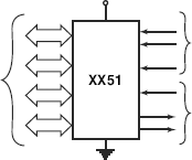
Externally, XX51 is a 40-pin IC in dual inline package (DIP). It is also available in other types of packaging, like plastic leaded chip carrier (PLCC) and thin quad flat pack (TQFP). However, for the present text we refer to the DIP. Schematically, major external features of XX51 are shown in Fig. 2.1.

Figure 2.1 XX51 schematic inputs and outputs
The signals seen on the right-hand side of Fig. 2.1 are for external world interfacing. These are called input/output (I/O) ports, or simply ports. There are a total of four such ports designated 0, 1, 2 and 3. Each of these four ports has eight I/O lines, which are bit-programmable. Being bit-programmable means that individually each port bit may be programmed as either input or output, irrespective of the condition of any other bits of that port.
Along the remaining three sides of XX51 of Fig. 2.1, all system input signals, necessary for running the device, are shown. These are power input [common-collector voltage (Vcc) and system ground potential (GND)], external crystal input for clock circuit (XTAL1 and XTAL2) and the RESET input. Power, as we can easily understand, is the most important input, without which the device would not function at all. External crystal input is necessary to generate the heartbeats of the processor. The third input signal, RESET, is necessary to initialize various features of the processor to make a fresh start.
Three more signals are shown at the left-hand side of the XX51 in Fig. 2.1. These [External Access ![]() , Program Store Enable
, Program Store Enable ![]() and Address Latch Enable (ALE)] are control signals to be used if the system demands interfacing of external memory. Otherwise, these signals are not used. We will discuss in details about these three signals along with the external memory interfacing in Chapter 17. However, at present, we mention only that if the external memory interfacing is not necessary, then the
and Address Latch Enable (ALE)] are control signals to be used if the system demands interfacing of external memory. Otherwise, these signals are not used. We will discuss in details about these three signals along with the external memory interfacing in Chapter 17. However, at present, we mention only that if the external memory interfacing is not necessary, then the ![]() input should be pulled high (connected with Vcc). Fig. 2.2 shows the schematic system inputs for the stand-alone operation of XX51. Note that a decoupling capacitor of 0.1 μF is necessary at Vcc to avoid unwanted high-frequency voltage oscillations at the power input.
input should be pulled high (connected with Vcc). Fig. 2.2 shows the schematic system inputs for the stand-alone operation of XX51. Note that a decoupling capacitor of 0.1 μF is necessary at Vcc to avoid unwanted high-frequency voltage oscillations at the power input.

Figure 2.2 Schematic system inputs for stand-alone operation
2.2 | Pins and Signals
Detailed pin-wise signals of XX51 (in 40-pin DIP) are presented in Fig. 2.3. A careful study reveals that some pins are associated with two signals, one of which is within a parenthesis. On the right, for ports 0 and 2, the signals in parenthesis are for external memory interfacing (address and data signals). These will be discussed in detail in Chapter 17. Signals at the left within parenthesis against port 3 are for interrupts, counters, control and serial interface, which would also be discussed further in Chapters 14, 15 and 16. Note that no alternate signal is associated with port 1. Here, we present a brief description of all major signals of the device.
Pins 32-39: Port 0 (P0.0–P0.7) is the only true bi-directional I/O port. External pull-up registers are necessary for this port to function properly as input or output. Low-order address and data bus signals are also multiplexed with this port for external memory interfacing. To serve as input, concerned bit(s) of this port must be written with 1s.
Pins 1-8: Port 1 (P1.0–P1.7) is a quasi-bi-directional I/O port. It is internally pulled up. To serve as input, concerned bit(s) of this port must be written with 1s. This port does not offer any alternate functions.

Figure 2.3 Pin-wise signal assignment of XX51
Pins 21-28: Port 2 (P2.0–P2.7) is also a quasi-bi-directional I/O port with internal pull-ups. To serve as input, concerned bit(s) of this port must be written with 1s. High-order address bus is multiplexed with this port for external memory interfacing.
Pins 10-17: Port 3 (P3.0–P3.7), like the previous two ports, is also a quasi-bi-directional with internal pull-ups. To serve as input, concerned bit(s) of this port must be written with 1s. Some alternate functions like interrupt input, timer/counter input and serial communication signals are shared with this port pins. Control signals necessary for external data memory interface, namely ![]() and
and ![]() , are also available from this port.
, are also available from this port.
Pin 9: RESET is the input for initializing the device during initial power-on or thereafter. To initialize, this input must remain high for a minimum of two machine cycles when the power is on and the system clock is active.
Pins 18, 19: XTAL1 and XTAL2 are to be used for interfacing an external crystal to generate the system clock. External clock source may also be used through these pins as discussed later in this chapter.
Pin 40: Vcc is for main power source input. Generally, it is 5V DC but the tolerance range varies from device to device.
Pin 20: Vss is provided for system ground reference (0V) connection.
Pin 30: ALE outputs signal as long as the device is operational. This signal is to be used for de-multiplexing the multiplexed address-data signal of port 0 during external memory interfacing. In each machine cycle, two ALE pulses are available. This signal may also be used to test whether the device is operational or not.
Pin 31: ![]() input is provided to allow or disallow the internal memory. Generally, this input is to be pulled high if internal program memory is to be used.
input is provided to allow or disallow the internal memory. Generally, this input is to be pulled high if internal program memory is to be used.
Pin 29: ![]() stands for Program Store Enable and may be taken as the substitute of the read signal for external program memory, interfaced with the device.
stands for Program Store Enable and may be taken as the substitute of the read signal for external program memory, interfaced with the device.
Is there any reason for making ![]() and
and ![]() as active low? Yes, there is. Some times unconnected inputs may generate high signal as input (specially for TTL inputs). Making these signals active low ensures that in no such unwanted cases the signal would trigger a false action.
as active low? Yes, there is. Some times unconnected inputs may generate high signal as input (specially for TTL inputs). Making these signals active low ensures that in no such unwanted cases the signal would trigger a false action.
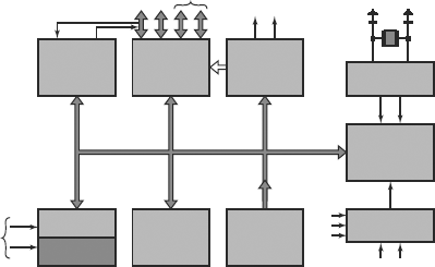
2.3 | Internal Architecture
Internally, XX51 is composed of an 8-bit data bus and a 16-bit address bus along with some control signals. All these form the system bus and important features like program memory (4K bytes), data memory (128 bytes), parallel ports (P0–P3), timers, serial interface, bus controller, interrupt controller, oscillator circuits along with the central processing unit are placed and interfaced with this system bus, as shown in Fig. 2.4. Note that serial port input and output, namely RxD and TxD, are interfaced with port 3 of the system, as alternate functions. We should now go for detailed discussions of program memory, data memory, system clock and reset features. Other internal parts of the microcontroller, like external interrupts, timers and serial interrupts, would be discussed later in Chapters 14, 15 and 16.

Figure 2.4 Simplified internal architecture of XX51
The reader may observe that in Fig. 2.4, the interfacing of program memory with the system bus is marginally different from other interfacing. We must remember that data bus is unidirectional from program memory while address and control bus directions are similar as other devices.
2.4 | Program Memory Organization
As indicated in Chapter 1, MCS-51 is designed around Harvard architecture, which distinguishes program memory from its data memory. Moreover, XX51 offers some amount of on-chip program memory and also a provision of expanding it by external interfacing of suitable non-volatile memory devices. Schematically, the organization of program memory of XX51 is explained through Fig. 2.5. Note that the ![]() input must be connected to GND if all instruction fetches must be performed from external program memory [Fig. 2.5(b)]. If
input must be connected to GND if all instruction fetches must be performed from external program memory [Fig. 2.5(b)]. If ![]() is connected with Vcc, then initial instruction fetches are performed from internal program memory. However, once the boundary is crossed, the fetch would automatically be performed from external program memory [Fig. 2.5(a)]. The maximum size of total program memory, internal plus external, may be 64K bytes for any configuration.
is connected with Vcc, then initial instruction fetches are performed from internal program memory. However, once the boundary is crossed, the fetch would automatically be performed from external program memory [Fig. 2.5(a)]. The maximum size of total program memory, internal plus external, may be 64K bytes for any configuration.

Figure 2.5 Arrangement of program memory in XX51 with (a) ![]() = 1 and (b)
= 1 and (b) ![]() = 0
= 0
As discussed earlier, to access external program memory, XX51 uses P0 and P2 ports for address and data bus. The signal, ![]() , is meant for program memory-read operations.
, is meant for program memory-read operations.
2.4.1 | Pipeline Architecture
In the previous chapter, in Table 1.3, it was indicated that 8051 adopted the pipeline architecture. A pipeline architecture allows the processor to fetch an instruction’s code during the decoding or execution time of its previous instruction. Intel 8086 microprocessor is capable of storing six such advanced bytes. 8051 also uses this pipeline architecture. However, it fetches and stores only one byte of the next instruction’s code in its pipeline.
Pipeline architecture makes a processor work faster. However, when the instructions are not in sequence, like program branching, etc., the pre-fetched code byte must be discarded or abandoned.
2.4.2 | Program Lock Bits
One important feature of program memory of MCS-51 is the program lock bits. These bits are provided to avoid unwanted software piracy. Once these lock bits are programmed, content of internal program memory cannot be read from the device by some outside circuit. However, if external program memory is also used, then these program lock bits cannot be utilized. A standard program memory-erase operation would unlock these lock bits but also would simultaneously erase the content of internal program memory completely.
It is not possible to implement any such program memory locking arrangement in a microprocessor based system as the program memory must be externally interfaced with the microprocessor.
2.5 | Data Memory Organization
Just like the program memory, the maximum size of external data memory may be 64K bytes. However, this 64K of data memory limit is irrespective of the amount of internal (on-chip) data memory. All versions of XX51 offer 128 bytes of internal data memory, while others, like XX52 and XX54, offer 256 bytes of internal data memory. In either case, the maximum allowable external data memory is 64K. Therefore, the maximum size of data memory for MCS-51 devices may be taken as 64K plus size of available internal data memory (128 or 256 bytes). The organization of internal and external data memory of XX51/52 is shown in Fig. 2.6.
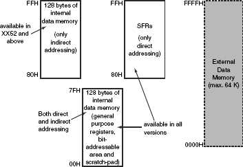
Figure 2.6 Arrangement of internal and external data memory of XX51/52
The internal data memory of 8051 is divided into three separate functional parts as
- register banks (address 00H to 1FH),
- bit-addressable area (address 20H to 2FH) and
- scratch-pad area (address 30H onwards).
This is shown in Fig. 2.7.
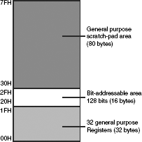
Figure 2.7 Major divisions of lower 128 bytes of internal RAM of XX51
2.5.1 | Register Banks
The lowest part of the internal RAM accommodates four general-purpose register banks designated as bank #0, #1, #2 and #3. Each bank contains eight general-purpose registers designated as R0, R1, R2 and so on, up to R7 as shown in Fig. 2.8. Multiple banks help in faster interrupt servicing. Out of these four banks, only one bank may be selected to be active at any time for operations. Whichever bank is selected, its registers may be addressed as R0, R1, R2, etc., by their respective nomenclature. This reduces the addressing time and generates faster response. However, the unselected bank’s registers may also be used by their direct addresses. Initially, after system reset, bank #0 is selected as default. This bank selection is achieved through the Program Status Word (PSW) register, which is described in the next chapter.
These registers may be used to store any data or an operand during arithmetic or logical operations. They can also be used as counters to count down. Registers R0 and R1 of the active bank may also be used as data pointers for indirect addressing. This would be discussed in greater details in Chapter 3 under the section titled Addressing Modes. If not used as registers, then they may be used as general-purpose storage area.
Example 2.1
Purpose: To understand the correlation between individual register names and their direct addresses. Note that they might be addressed in both ways, if they are within the active register bank.
Problem
Assume that at present, register bank #1 is selected. Which of its registers would be addressed by the direct address 0AH, when some other bank is selected?
Solution
Referring to Fig. 2.8, we observe that the direct address 0AH belongs to register R2 of bank #1. Therefore, the correct answer is R2.

Figure 2.8 Organization of register banks and general-purpose registers
2.5.2 | Bit-Addressable Area
Next 16 bytes after four register banks, starting from address 20H to 2FH, contain 128 bits in total and are designated as bit-addressable area. Each one of these 128 bits has an individual bit address varying from 00H to 7FH. This area is expected to store bit variables for the application program.
In many control operations, the data might be of a single bit rather than a full byte. For example, the condition of a motor, running or not, may be represented through a single bit. Using a full byte for storage of this information is not necessary. Bit-addressable area helps the software developer to store these types of Boolean variables resulting in economical usage of the system memory. If not used for bit-variable storage, then such unused bytes of this area may also be used to store information in the form of bytes. Both byte and bit addresses within this area are shown in Fig. 2.9.

Figure 2.9 Bit-addressable area of RAM with bit addresses
Example 2.2
Purpose: To correlate directly addressable bits’ physical locations in RAM and their individual addresses.
Problem
- What would be the address of bit 5 (bit 0 being LSB) of internal RAM location 2BH?
- Indicate the location of the bit whose bit address is 37H.
- Where is the bit E7H?
Solution
- Referring to Fig. 2.9, we find that the direct address of bit 5 of RAM location 2BH is 5DH.
- Referring to Fig. 2.9, it is bit 7 (MSB) of the byte with the address 26H.
- The bit addresses of the bit-addressable area vary from 00H to 7FH. Therefore, the bit is outside the bit-addressable area. (E7H is MSB of accumulator to be discussed in the next chapter).
2.5.3 | Scratch-Pad Area
The last part of the internal RAM area, from 30H to the rest, may be used for any general-purpose storage including the stack. It may be noted here that after system reset, the stack pointer (SP) is initialized at 07H so that the stack may start from 08H onwards. Any unused bytes of the bit-addressable area or unused register banks may also be used for general-purpose data storage.
For XX51 devices, the highest address of scratch-pad area is 7FH. However, for XX52, XX54, etc., the highest address is FFH as the size of on-chip RAM is 256 bytes. In this context, it may be noted that the higher 128 bytes if available on-chip, then it may only accessed by indirect addressing (through R0 and R1) and not by direct addressing. The lower 128 bytes of RAM, present in all systems, may be addressed both directly as well as indirectly (refer to Fig. 2.6).
2.6 | System Clock
The system clock in a processor is as important as the heartbeat of a human body. All duties performed by a processor are basically dependent on this system clock. As a normal practice, this clock is driven by an external quartz crystal attached with XTAL1 (pin 19) and XTAL2 (pin 18) of XX51, as shown in Fig. 2.10(a). It is a normal practice to use quartz crystals as they produce accurate oscillations.

Figure 2.10 Oscillator circuit with (a) external crystal, (b) external TTL clock source for HMOS device and (c) external CMOS clock source for CHMOS device
However, if necessary, external clock sources may also be used to drive the system clock. For a HMOS device, this external clock signal may be applied to XTAL2 (pin 18) while XTAL1 (pin 19) must be grounded, as shown in Fig. 2.10(b). For a CHMOS device, this external clock signal must be supplied at XTAL1 (pin 19) while XTAL2 (pin 18) input must be left as it is [refer to Fig. 2.10(c)].
The allowable maximum and minimum clock frequency varies from device to device. A general practice is to use an external crystal of 12 MHz frequency unless serial communications are necessary. For the systems using serial communications facilities, a crystal of frequency 11.0592 MHz is more appropriate as the standard baud rates (9600, 4800, etc.) may easily be generated using this frequency (refer to Chapter 16 for further explanations).
Internally, multiple numbers of this system clock oscillation are used for various purposes. If we designate each complete oscillation of the external crystal or clock source as a pulse, then two such pulses produce a state. Six states generate one machine cycle. Instructions need one, two or four such machine cycles for fetching the opcode and its execution (Fig. 2.11).
We have previously been introduced to the ALE signal of XX51. Two pulses of this ALE signal are available for each machine cycle. A quick method to check whether an XX51 is functioning properly or not is to monitor this ALE signal through an oscilloscope. As a normal practice, every machine cycle would generate two ALE pulses as shown in Fig. 2.11.
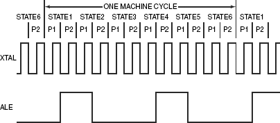
Figure 2.11 System clock for one machine cycle
Fig. 2.11 shows that 12 clock pulses are incorporated within a machine cycle. As MCS-51 depends on micro-programming or micro-coding, therefore so many pulses are necessary. Micro-programming reduces the hardware overhead for instruction decoding and its execution at the cost of the speed of execution.
2.7 | Reset
Reset, or power-on reset, is an another important feature of any processor. For XX51, this reset must be active high for at least two machine cycles (or 24 oscillator periods). During this time, many internal registers are initialized. The program counter (PC) is also cleared so that the first instruction, to be executed after reset, is fetched from address 0000H. Fig. 2.12(a) shows the standard power-on reset circuit, suitable for XX51. For manual reset operation without switching off and on the power input, a reset switch might be connected in parallel with the 10 μF capacitor [Fig. 2.12(b)].
Reset does not change the content of internal RAM of the system. However, after power-on reset, content of this internal RAM is unpredictable. In either case, following are the four major actions implemented by a system reset:
- PC is cleared,
- stack pointer (SP) is initialized by 07H (system stack starts from 08H),
- register bank #0 is selected and
- all ports output FFH.
Table 2.1 below indicates the conditions of all Special Function Registers (SFRs) after reset. These reset values are in binary. Conditions of the bits, marked as ‘X’, remain undefined after reset.

Figure 2.12 (a) Power-on reset circuit and (b) with manual reset option
Table 2.1 Reset values for XX51
| Register | Reset value (B) | Remarks |
|---|---|---|
| A | 00000000 | |
| B | 00000000 | |
| DPTR | 00000000 00000000 | |
| IE | 0XX00000 | All interrupts disabled |
| IP | XXX00000 | |
| P0 | 11111111 | Output FFH, ready to read |
| P1 | 11111111 | Output FFH, ready to read |
| P2 | 11111111 | Output FFH, ready to read |
| P3 | 11111111 | Output FFH, ready to read |
| PC | 00000000 00000000 | Address of first instruction |
| To be executed after reset | ||
| PCON | 0XXXXXXX | Timer 1 as baud rate gen. |
| Power-saving modes unpredictable | ||
| PSW | 00000000 | Selects register bank #0 |
| SBUF | XXXXXXXX | |
| SCON | 00000000 | |
| SP | 00000111 | Stack from 08H onwards |
| TCON | 00000000 | Stop both timers |
| TH0 | 00000000 | |
| TH1 | 00000000 | |
| TL0 | 00000000 | |
| TL1 | 00000000 | |
| TMOD | 00000000 |
To understand various operations performed by the processor during and after reset, we have to be familiar with some of the SFRs of XX51. These will be studied in the next chapter.
When the system or microcontroller is switched on, the reset generated is called power-on reset or cold start. Without switching off and on the power, if manual reset key is pressed, then it is known as warm start. We shall discuss more about it in the power management chapter (Chapter 24).
2.8 | How to Program 8051
We already know that MCS-51 microcontrollers offer 4K bytes (or more, depending upon the version) of on-chip program memory to store the program which would be executed when the system is switched on. Any beginner is curious to know that how a program, written on a piece of paper, may be placed inside this program memory of the microcontroller chip. In this section we discuss about the procedure regarding how to load the program memory of a microcontroller by the program, developed by the system designer.
2.8.1 | Overview of Programming
Any program, as we all know, is composed of several instructions. In this book, the complete instruction set of MCS-51 is presented in Appendix-B and explained in chapters 4 to 12. Several example programs are also presented throughout the book and we assume that presently we are ready with one such example program, composed of MCS-51 instructions, written on a piece of paper. The reader may note that a program written using this instruction set is known as assembly language program. The next step would be to transfer this assembly language program within the program memory inside the microcontroller chip (IC). We already know that this program memory may store several groups of bits and presently our program is not composed of bits but instructions. Therefore, these instructions of our program are to be translated into corresponding bits.
To implement this translation and putting translated bits inside microcontroller chip, we shall require the service of an universal programmer and few more software tools. This universal programmer must be interfaced with any standard PC. Apart from offering necessary interfacing connections for PC (USB or similar) every universal programmer has a ZIF (Zero Insertion Force) socket to insert or remove any IC (to be programmed) easily, without the need of any external additional force. For this purpose all ZIF sockets are equipped with a mechanical lever which, when turned, grips or releases all IC pins simultaneously. The IC to be programmed must be inserted within this ZIF socket of the universal programmer.
The overall procedure for programming any microcontroller chip is as follows:
- Develop the program using an editor.
- Translate the program to binary using an assembler.
- Transfer the binary data within the microcontroller using universal programmer.
We shall now discuss these steps with adequate details in following sections.
2.8.2 | Editor
To develop the assembly language program, we shall need the help of an editor. Editor is a software tool which allows us to freely type the program and save it as and when necessary. Apparently, this editor functions very much similar to any word-processing software. We may type our already developed software from paper to the editor as a new file. Alternately, we may use the editor to write necessary instructions one after another and finish our program development. Remember that the final outcome from the editor is always a file containing the soft copy of the program composed of MCS-51 instruction set. We should save this file before proceeding to the next step, where this file would be used as the source file.
2.8.3 | Assembler
Once software writing part is complete using the editor, help of an assembler is necessary to generate the binary code of each instruction of the program. Assembler is a software which accepts any program (source file) written in assembly language (using instruction set) and generates the executable machine code in binary. Depending upon the type of assembler, this conversion or translation may be completed in one-pass, two-pass, or multi-pass. The binary output file created by the assembler is to be saved for further use. The reader may note that assembler is processor dependent and for our purpose we shall need a MCS-51 assembler.
2.8.4 | Burning the Chip
The binary code, generated by the assembler, is to be fed within the microcontroller chip. This duty is carried out by the universal programmer and the process is known as burning the chip. To implement it, the microcontroller chip is to be plugged into the ZIF socket of the universal programmer. The ‘program’ command by clicking the mouse would transfer the bytes of binary output file (generated by the assembler) into the program memory within the microcontroller chip. After this, the microcontroller chip may be taken out of the ZIF socket of the universal programmer and may be fitted within the circuit board for functioning. Some microcontrollers offer in-circuit burning facility, means, they need not be fitted within the ZIF socket of the universal programmer, burnt, and then to be taken out and fitted within the circuit board. Rather the circuit, with the microcontroller to be programmed, is to be connected with the universal programmer through USB or other suitable interface and the burning operation may be implemented.
2.8.5 | IDE
Commercially, in most of the cases, the editor, assembler and other related software tools (like: debugger, simulator, etc.) are available as a single package which is known as IDE or integrated development environment. In remaining cases, they are available as separate software packages and to be individually executed.
The term IDE was originally introduced by Borland Corporation through their now-famous product, Turbo Pascal. Thereafter the concept of IDE became popular and was adopted by many software vendors. In case, of microcontrollers, some commercially available IDE packages offer data bases of different types of microcontrollers and an interactive, user-friendly package for solving all software development related problems.
SUMMARY
XX51 external pins and signals and internal architecture along with clock and reset operations are discussed in this chapter.
Externally, XX51 is available in a 40-pin DIP. Apart from four 8-bit bit-programmable I/O ports designated as P0, P1, P2 and P3, it also offers pins for power (5V DC) input, crystal oscillator connectors, active high reset input, external memory access allowing input ![]() and two control signals (output) for external memory interface, namely
and two control signals (output) for external memory interface, namely ![]() and ALE. When interfaced with external memory, ports P0 and P2 are used for multiplexed address (16) and data (8) signals.
and ALE. When interfaced with external memory, ports P0 and P2 are used for multiplexed address (16) and data (8) signals.
Internally, XX51 contains a 8-bit processor, 4K program memory, 128 bytes of data memory, two 16-bit timer/counters, interrupt handling circuits and a serial communication interface. Provision is there to lock this internal program memory using lock bits to avoid unwanted software piracy. Internal data memory of 128 bytes includes four general-purpose register banks of eight registers each, 16 bytes of bit-addressable area and 80 bytes of scratch-pad area. Out of four register banks, only one is active at any time and selectable through PSW register. Registers R0 and R1 of the selected bank may also be used as pointers.
The system clock may be generated by either using a quartz crystal or an external clock source. Every machine cycle is composed of 12 oscillator periods or six states. XX51 accepts an active high reset input, which should remain high for two consecutive machine cycles. Apart from initializing various internal registers, this reset clears PC, loads SP by 07H, selects register bank #0 and outputs FFH through all ports.
POINTS TO REMEMBER
- Only one of four register banks would be active any time, providing eight general-purpose registers from R0 to R7.
- Contents of bits 3 and 4 of PSW SFR select the active register bank at any time of operation.
REVIEW QUESTIONS
Evaluate Yourself
- The number of pins for a XX51 in DIP is
- 20
- 40
- 48
- none of these
- Which of the following statements is false?
- All XX51 ports are bi-directional
- All XX51 ports are bit-programmable
- All XX51 ports output FFH after reset
- All XX51 ports need external pull-ups
 may be taken as
- READ signal for external memory
- WRITE signal for external memory
- Either of the above two
- none of these
- The size of on-chip program memory for XX51 is
- 4K bytes
- 8K bytes
- 16K bytes
- none of these
- The size of on-chip data memory for XX51 is
- 64 bytes
- 128 bytes
- 256 bytes
- none of these
- One machine cycle of XX51 takes
- 12 clock pulses
- 6 states
- Both of these
- none of these
- Reset input of XX51 should remain high for
- 1 machine cycle
- 2 states
- 3 clock periods
- none of these
- Reset input for XX51
- clears all ports
- loads SP by 00H
- selects bank #1
- none of these
- For a power-on reset circuit of XX51, the capacitor should be of
- 0.001 μF
- 0.01 μF
- 10 μF
- none of these
- After reset, PCON register is initialized as
- 0xxxxxxx
- x0000000
- xxxxxxxx
- none of these
Search for Answers
- Try to annotate the following functional block diagram of XX51.
- What is the major difference between port 0 and the other three ports of XX51?
- What is the purpose of the ALE signal?
- Try to annotate the following simplified schematic diagram indicating internal architecture of XX51.
- What is locked by program lock bits? What is the purpose of providing this?
- How should the following on-chip data memory locations be addressed?
- Lower 128 bytes from 00H to 7FH.
- Upper 128 bytes from 80H to FFH.
- Special function registers located within 80H to FFH.
- At any time how many general-purpose registers located between 00H and 1FH of XX51 may be used? Why R0 and R1 are different from the remaining registers?
- If bit 0 is taken as LSB and bit 7 as the MSB, then what would be the bit-address of bit 3 of internal data memory location 29H?
- In general, a 12 MHz crystal is used for XX51-based systems. However, in certain cases, a frequency of 11.0592 is preferred. What is the reason behind it?
- What is the relation between machine cycle, state and pulse for any XX51 microcontroller?
Think and Solve
- Why is it important to study the reset initialization details of any microcontroller? Are the internal RAM locations cleared by a system reset?
- What is the maximum total size of data memory, which may be directly addressed by the 8752 microcontroller? What type of address bus makes it possible?
- What purpose does the pair of 33 pF capacitor serve in the external crystal circuit? What would happen if these two capacitors are removed from an otherwise perfectly working circuit?
- Would the reset circuit function properly if its 8.2K resistor is replaced by a 10K resistor? Justify your answer.
- Is the following circuit sufficient for a power-on reset?

- What is the maximum size of stack possible for any XX51 microcontroller? Would this size remain same for an XX52 microcontroller?
- What is the width (number of bits) of the address bus for internal data memory of XX52?
- What is the purpose of providing multiple numbers of register banks in XX51?
- Why all ports output FFH after a system reset?
- Why Princeton architecture was not used in MCS-51?