
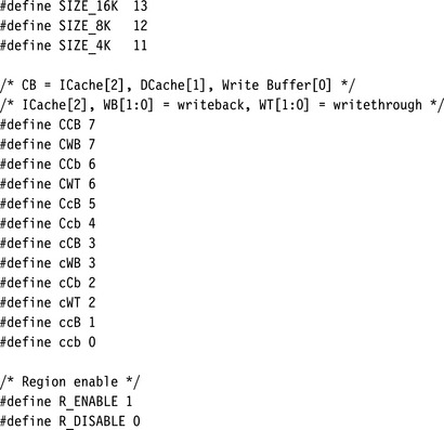
MEMORY PROTECTION UNITS
13.2. INITIALIZING THE MPU, CACHES, AND WRITE BUFFER
Some embedded systems use a multitasking operating or control system and must ensure that a running task does not disrupt the operation of other tasks. The shielding of system resources and other tasks from unwanted access is called protection and is the subject of this chapter.
There are two methods to control access to system resources, unprotected and protected. An unprotected system relies solely on software to protect the system resources. A protected system relies on both hardware and software to protect the system resources. The choice of method used by the control system depends on the capability of the processor and the requirements of the control system.
An unprotected embedded system has no hardware dedicated to enforcing the use of memory and peripheral devices during operation. In these systems, each task must cooperate with all other tasks when accessing system resources because any task could corrupt the state of another task. This cooperative scheme may result in task failure when one task ignores the access limits of another task’s environment.
An example of a task failure that might occur in an unprotected system involves reading and writing to a serial port register for communication. If one task is using the port, there is no way to prevent another task from using the same port. Successful use of the port must be coordinated through a system call that provides access to the port. An unauthorized access by a task working around these calls can easily disrupt communications through the port. The undesirable use of the resource could be unintentional, or it could be hostile in nature.
In contrast, a protected system has dedicated hardware to check and restrict access to system resources. It can enforce resource ownership. Tasks are required to behave by a set of rules defined by the operating environment and enforced by hardware, which grants special privileges to the programs that monitor and control resources at the hardware level. A protected system is proactive in preventing one task from using the resources of another. The use of hardware to actively monitor the system provides better protection than cooperatively enforced software routines.
ARM provides several processors equipped with hardware that actively protects system resources, either through a memory protection unit (MPU) or a memory management unit (MMU). A processor core with an MPU, the subject of this chapter, provides hardware protection over several software-designated regions. A processor core with an MMU, the subject of the next chapter, provides hardware protection and adds a virtual memory capability.
In a protected system, there are two major classes of resource that need monitoring: the memory system and peripheral devices. Since ARM peripherals are generally memory mapped, the MPU uses the same method to protect both resources.
An ARM MPU uses regions to manage system protection. A region is a set of attributes associated with an area of memory. The processor core holds these attributes in several CP15 registers and identifies each region by a number, which ranges between zero and seven.
A region’s memory boundaries are configured using two attributes, the starting address and its length, which can be any power of two between 4 KB and 4 GB. In addition, the operation system assigns additional attributes to these regions: access rights and the cache and write buffer policies. The access to a region in memory is set as read-write, read-only, or no access and is subject to additional rights based on the current processor mode, which is either privileged or user. A region also has a cache write policy, which controls cache and write buffer attributes. For example, one region can be set to access memory using a writethrough policy, while another operates as noncached and nonbuffered.
When the processor accesses a region in main memory, the MPU compares the region’s access permission attributes with the current processor mode to determine what action it will take. If the request satisfies the region access criteria, the core is allowed to read or write to main memory. However, if the memory request results in a memory access violation, the MPU will generate an abort signal.
The abort signal is routed to the processor core, where it responds to the abort signal by taking an exception and vectoring to the abort handler. The abort handler then determines the abort type as either a prefetch or data abort, and based on the abort type the handler branches to the appropriate service routine.
To implement a protected system, the control system defines several regions to different areas in main memory. A region may be created once and last for the life of the embedded system or may be created temporarily to satisfy the needs of a specific operation and then removed. How to assign and create regions is the subject of the next section.
13.1 PROTECTED REGIONS
There are currently four ARM cores that contain an MPU; the ARM740T, ARM940T, ARM946E-S, and the ARM1026EJ-S. The ARM740T, ARM946E-S, and ARM1026EJ-S each contain 8 protection regions; the ARM940T contains 16 (see Table 13.1).
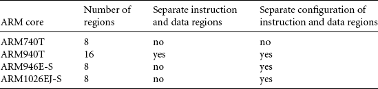
The ARM740T, ARM946E-S, and ARM1026EJ-S have unified instruction and data regions—the data region and instruction region are defined using the same register that sets the size and starting address. The memory access permission and cache policies are configured independently for instruction and data access in the ARM946E-S and ARM1026EJ-S cores; in the ARM740T the same access permission and cache policies are assigned to both instruction and data memory. Regions are independent of whether the core has a Von Neumann or Harvard architecture. Each region is referenced by an identifying number between zero and seven.
Because the ARM940T has separate regions to control instruction and data memory, the core can maintain different region sizes and starting addresses for instruction and data regions. The separation of instruction and data regions results in eight additional regions in this cached core. Although the identifying region numbers in an ARM940T still range from zero to seven, each region number has a pair of regions, one data region and one instruction region.
There are several rules that govern regions:
1. Regions can overlap other regions.
2. Regions are assigned a priority number that is independent of the privilege assigned to the region.
3. When regions overlap, the attributes of the region with the highest priority number take precedence over the other regions. The priority only applies over the addresses within the areas that overlap.
4. A region’s starting address must be a multiple of its size.
5. A region’s size can be any power of two between 4 KB and 4 GB—in other words, any of the following values: 4 KB, 8 KB, 16 KB, 32 KB, 64 KB, …, 2 GB, 4 GB.
6. Accessing an area of main memory outside of a defined region results in an abort. The MPU generates a prefetch abort if the core was fetching an instruction or a data abort if the memory request was for data.
13.1.1 OVERLAPPING REGIONS
Overlapping regions occur when some portion of the memory space assigned to one region is also in the memory space assigned to another region. Overlapping regions provide a greater flexibility when assigning access permission than nonoverlapping regions.
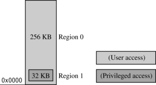
For an example of overlapping regions, suppose a small embedded system has 256 KB of available memory starting at address 0×00000000 and must protect a privileged system area from user mode reads and writes. The privileged area code, data, and stacks fit in a 32 KB region starting, with the vector table, at 0×00000000. The remaining memory is assigned to user space.
With overlapping regions, the system uses two regions, a 256 KB user region and a 32 KB privileged region (see Figure 13.1). The privileged region 1 is given the higher number because its attributes must take precedence over the user region 0.
13.1.2 BACKGROUND REGIONS
Another useful feature provided by overlapping regions is a background region—a low-priority region used to assign the same attributes to a large memory area. Other regions with higher priority are then placed over this background region to change the attributes of a smaller subset of the defined background region. So the higher-priority region is changing a subset of the background region attributes. A background region can shield several dormant memory areas from unwanted access while another part of the background region is active under a different region’s control.
For example, if an embedded system defines a large privileged background region, it can lay a smaller unprivileged region over this background. The location of the smaller region can be moved over different areas of the background region to reveal different user spaces. When the system moves the smaller user region from one location to another, the previously covered area becomes protected by the background region. So the user region is acting as a window allowing access to different parts of the privileged background but has user-level attributes (see Figure 13.2).
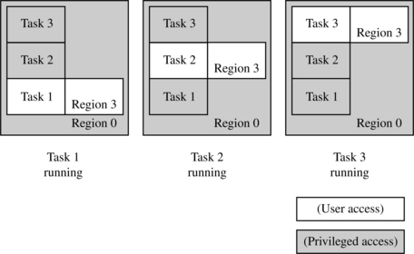
Figure 13.2 shows a simple three-task protection scheme. Region 3 defines the protection attributes of the active task, and the background region 0 controls access to the other tasks when they are dormant. When task 1 is running, the background region protects tasks 2 and 3 from task 1. When task 2 is running, tasks 1 and 3 are protected. Finally, when Task 3 is running, tasks 1 and 2 are protected. The reason this works is that region 3 has higher priority than region 0, even though region 0 has higher privilege.
We use a background region in the example code at the end of this chapter to demonstrate a simple multitasking protection scheme.
13.2 INITIALIZING THE MPU, CACHES, AND WRITE BUFFER
In order to initialize the MPU, caches, and write buffer, the control system must define the protection regions required during the target operation.
At a minimum the control system must define at least one data region and one instruction region before it can enable the protection unit. The protection unit must be enabled before or at the same time as the caches and write buffer are enabled.
The control system configures the MPU by setting primary CP15 registers c1, c2, c3, c5, and c6. Table 13.2 lists the primary registers needed to control the operation of the MPU. Register c1 is the primary control register.
Table 13.2
Coprocessor registers that control the MPU.
| Function | Primary register | Secondary registers |
| System control | c1 | c0 |
| Region cache attributes | c2 | c0 |
| Region write buffer attributes | c3 | c0 |
| Region access permissions | c5 | c0 |
| Region size and location | c6 | c0 to c7 |
Configuring registers c2 and c3 sets the cache and write buffer attributes of regions. Register c5 controls region access permissions. There are 8 or 16 secondary registers in register c6 that define the location and size of each region. There are other configuration registers in the ARM740T, ARM940T, ARM946E-S, and ARM1026EJ-S, but their use does not involve the basic operation of the MPU. To review the use of coprocessor 15 registers, refer to Section 3.5.2.
The following steps are required to initialize the MPU, caches, and write buffer:
1. Define the size and location of the instruction and data regions using CP15:c6.
2. Set the access permission for each region using CP15:c5.
3. Set the cache and write buffer attributes for each region using CP15:c2 for cache and CP15:c3 for the write buffer.
For each of these steps, there is a chapter section that follows describing the coprocessor 15 commands needed to configure each register. There is also example code showing the commands used in a routine that completes the step in the initialization process.
13.2.1 DEFINING REGION SIZE AND LOCATION
To define the size and address range of each region, the embedded system writes to one of the eight secondary registers, CP15:c6:c0:0 to CP15:c6:c7:0. Each secondary coprocessor register number maps to the corresponding region number identifier.
The starting address for each region must be aligned on an address that is a multiple of its size. For example, if a region is 128 KB in size, it can start at any address multiple of 0×20000. The size of a region can be any power of two from 4 KB to 4 GB.
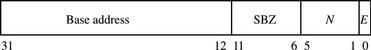
The bit fields and the format of the eight secondary registers CP15:c6:c0 to CP15:c6:c7 are shown in Figure 13.3 and Table 13.3. The starting address is stored in the top bit field [31:20] and must be a multiple of the size bit field [5:1]. The E field bit [0] enables or disables the region; that is, a region can be defined and disabled so that its attributes are not enforced until the enable bit is set. The unused bits in the CP15:c6 secondary registers should be set to zero.
Table 13.3
Bit field description of registers CP15:c6:c0 to CP15:c6:c7.
| Field name | Bit fields | Comments |
| Base address | [31:12] | Address greater than 4 KB must be a multiple of the size represented in [5:1] |
| SBZ | [11:6] | Value “should be zero” |
| N | [5:1] | Size of region is 2N+1, where 11 ≤ N ≤ 31 |
| E | [0] | Region enable, 1 = enable, 0 = disable |
To define the size of a region, you can use the formula, size = 2N+1 or look up the value in Table 13.4. To set the size, place the exponent value N in the size bit field of the CP15:c6 register. The value of N is limited by the hardware design to be any integer between 11 and 31, representing 4 KB to 4 GB. The binary value provides the exact bit field for the size entry. Once you have determined the size of a region, the starting address of the region can be any integer value times the size calculated from the formula, or if you like, taken from Table 13.4. The region size and starting address are determined by the memory map of your system and the areas the control system must protect. The demonstration system at the end of this chapter shows how to set up regions given a system memory map.
Table 13.4
| Size | Decimal value | Binary value |
| 4 KB | 11 | 01011 |
| 8 KB | 12 | 01100 |
| 16 KB | 13 | 01101 |
| 32 KB | 14 | 01110 |
| 64 KB | 15 | 01111 |
| 128 KB | 16 | 10000 |
| 256 KB | 17 | 10001 |
| 512 KB | 18 | 10010 |
| 1 MB | 19 | 10011 |
| 2 MB | 20 | 10100 |
| 4 MB | 21 | 10101 |
| 8 MB | 22 | 10110 |
| 16 MB | 23 | 10111 |
| 32 MB | 24 | 11000 |
| 64 MB | 25 | 11001 |
| 128 MB | 26 | 11010 |
| 256 MB | 27 | 11011 |
| 512 MB | 28 | 11100 |
| 1 GB | 29 | 11101 |
| 2 GB | 30 | 11110 |
| 4 GB | 31 | 11111 |
The ARM740T, ARM946E-S, and ARM1026EJ-S processors each have eight regions. To set the size and location of a region requires a write to a secondary register in CP15:c6:cX. For example, the instruction syntax needed to set the location and size of region 3 to start
at 0×300000 with a size of 256 KB is
![]()
The core register r1 is filled with the required bit field data; then it is written to the CP15 secondary register using an MCR instruction.
The ARM940T has eight instruction regions and eight data regions. The regions require an additional opcode2 modifier to select either the instruction or data region. Opcode2 is zero for data regions and one for instruction regions.
For example, to read the size and location of data and instruction region 5 requires two MRC instructions, one for the instruction region and one for the data region. The instructions needed to read the size and starting location of the regions are
![]()
The first instruction loads core register r2 with the size and starting address of data region 5, and the second instruction loads core register r3 with the size and starting address of instruction region 5. The ARM940T is the only processor core that has separate instruction and data regions.
EXAMPLE 13.1
The following example code shows how to set the starting address, size of a region, and the enable bit. The routine regionSet has the following C prototype:
![]()
The routine has four unsigned integer inputs: the region to configure, the starting address of the region, the encoded sizeN of the region, and whether the region is enabled or disabled. It is a good idea to disable a region while changing its attributes and then reenabling it when the changes are complete.
To make the routine work for all four available versions of an MPU processor, we unified the ARM940T region space by configuring the instruction and data regions with the size and starting address information. To do this, we wrote a macro called SET_REGION with two parts, one for the ARM940T and one for the other cores. This allows the same routine to support the four MPU cores.
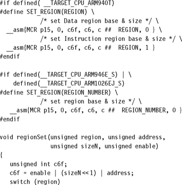
The code starts by merging the region attributes of starting address, sizeN, and enable into an unsigned integer named c6f. The routine then branches to one of eight regionSet routines created using the macro SET_REGION, which sets the region’s starting address, size, and enable state by writing to CP15:c6 secondary register for the region defined.
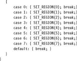
13.2.2 ACCESS PERMISSION
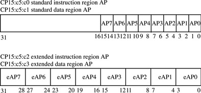
There are two sets of access permission schemes available, a standard set and an extended set. All four cores support the standard set, which provides four levels of permission. The newer ARM946E-S and ARM1026EJ-S support an extended set, which adds an additional two levels of permission (see Table 13.5). The extended set AP (access permission) bit field encoding supports 12 additional permission values. Only two of these bits have been allocated to date. Using an undefined encoding results in unpredictable behavior.
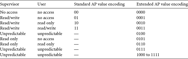
To assign access permission to a region requires a write to a secondary register in CP15:c5. Secondary registers CP15:c5:c0:0 and CP15:c5:c0:1 configure standard AP, and secondary registers CP15:c5:c0:2 or CP15:c5:c0:3 configure extended AP. Table 13.6 and Figure 13.4 show the register’s permission bit assignments for the AP registers.
Processors that support extended permission can also run software written for standard permission. The type of permission in effect depends on the last write to a CP15 AP register: If the last written AP register was a standard AP register, then the core is using standard permission; if the last written AP register was an extended AP register, then the core uses extended permission. This works because a write to the standard AP registers also updates the extended AP registers, meaning that the high bits [2:3] of the extended AP region entry are cleared.
When using standard AP, each region has two bits in registers CP15:c5:c0:0 and CP15:c5:c0:1. CP15:c5:c0:0 sets the AP for data, and CP15:c5:c0:1 sets the instruction region.
To read the standard AP for instruction and data memory requires reading two registers. The following two MRC instruction sequence places AP information for data region memory in core register r1 and AP information for instruction region in register r2:
![]()
When using extended AP, each region uses four bits in registers CP15:c5:c0:2 and CP15:c5:c0:3. The core stores instruction information for the eight regions in a single register and the data information in another register. CP15:c5:c0:2 sets the AP for the data region, and CP15:c5:c0:3 sets the AP for the instruction region.
Obtaining the instruction and data region extended AP requires reading two registers. The following two-instruction sequence places region data AP in core register r3 and region instruction AP in register r4:
![]()
We supply two examples to demonstrate using access permissions, one for standard AP and the other for extended AP. These examples use the inline assembler to read and write to the CP15 registers.
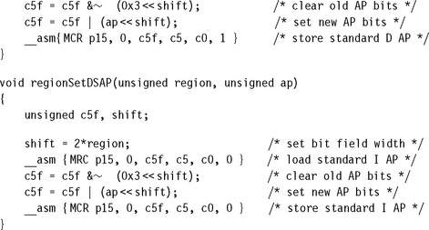
We provide two standard AP routines, regionSetISAP and regionSetDSAP, to set the standard AP bits for a region. They are called from C using the following function prototype:
![]()
The first parameter is the region number, and the second is the two-bit value defining the standard AP for the instruction or data memory controlled by the region.
EXAMPLE 13.2
The two routines are identical with the exception that they read and write to different CP15:c5 secondary registers; one writes to the instruction register, and the other to the data register. The routine does a simple read-modify-write operation on the CP15:c5 register to set the AP of the specified region, leaving the remaining regions intact.
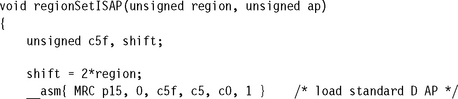
The routine sets the specified region permissions by clearing its AP bits using a shifted mask value and then setting the AP bit field with the ap input parameter. The AP bit field location is calculated as the region size times the number of bits in the permission bit field; this is the shift variable. The value of the bit field is set by shifting the ap value and using an OR to modify the c5f core register.
We provide two extended AP routines, regionSetIEAP and regionSetDEAP, to set the extended AP bits for a region. They have the following C function prototypes:
![]()
The first parameter is the region number, and the second is the four-bit value representing the extended AP for the instruction or data memory controlled by the region.
EXAMPLE 13.3
The two routines are identical to the standard AP routines with the exception that they read and write to different CP15:c5 secondary registers and they have a four-bit-wide AP bit field.
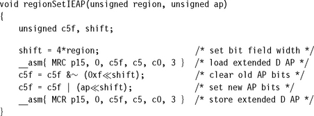

Each routine sets the specified region permissions by clearing its AP bits using a shifted mask value and then setting the AP bit field with the ap input parameter. The AP bit field location is calculated as the region size times the number of bits in the permission bit field; this is the shift variable. The value of the bit field is set by shifting the ap value and using an OR to modify the c5f core register.
13.2.3 SETTING REGION CACHE AND WRITE BUFFER ATTRIBUTES
Three CP15 registers control the cache and write buffer attributes for each core. Two registers, CP15:c2:c0:0 and CP15:c2:c0:1, hold the D-cache and I-cache region attributes. A third, CP15:c3:c0:0, holds the region write buffer attributes and applies to memory data regions. (Refer to Figure 13.5 and Table 13.7 for details.)
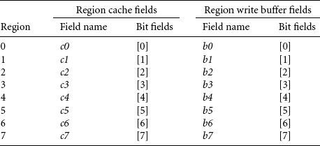
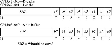
Register CP15:c2:c0:1 contains the cache configuration data for all eight instruction regions, and register CP15:c2:c0:0 contains all eight data regions. Both registers use the same bit field encoding.
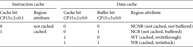
The cache bit determines if the cache is enabled for a given address within the region. In the ARM740T and ARM940T, the cache is always searched, regardless of the state of the cache bit. If the controller finds a valid cache entry, it will use the cached data over data in external memory.
Because of this cache behavior, you need to flush and possibly clean the cache in a region where the cache policy changes from cached to noncached. Consequently, the MPU control system must always flush the cache when changing the cache policy from writethrough to noncached. It must always clean and flush the cache when changing the cache policy from writeback to noncached. It must also clean the cache when changing the cache policy from writeback to writethrough. See Chapter 12 for routines to clean and/or flush the cache.
In the ARM946E-S, if the cache bit is clear, information physically in cache will not be returned from the cache, and an external memory access is performed instead. This design lightens the requirement to flush the cache when it is disabled. However, the cleaning rules for the old region still apply.
The eight region write buffer bits in the register CP15:c3:c0:0 enable or disable the write buffer for each region (again see Figure 13.5).
When configuring data regions, the region cache and write buffer bits together determine the policy of the region. The write buffer bit has two uses; it enables or disables the write buffer for a region and sets the region cache write policy. The region cache bit controls the purpose of the write buffer bit. When the cache bit is zero, the buffer bit enables the write buffer when its value is one and disables the write buffer when its value is zero. When the cache bit is set to one, the cache and write buffer are both enabled and the buffer bit determines the cache write policy. The region uses a writethrough policy if the buffer bit is zero and a writeback policy if the buffer bit is set. Table 13.8 gives a tabular view of the various states of the cache and write buffer bits and their meanings. For more details on writeback and writethrough policies, see Section 12.3.1.
We supply two routines to demonstrate enabling and disabling the caches and write buffer. The two routines use the inline assembler to read and write to the CP15 registers.
We combine control of the cache and write buffer into a single routine call to simplify system configuration. We reference both the data cache and write buffer bits by the write policy they control, and the instruction cache bit stands alone. From a system view, merging the state of the caches and write buffer into a single value for each region makes it easier to group region information into a region control block (discussed in Section 13.3.3).
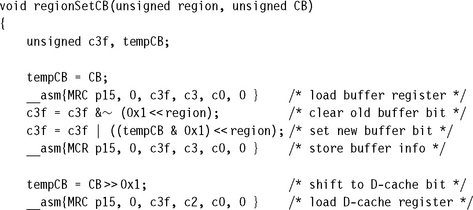
The set cache and buffer routine, called regionSetCB, is shown in Example 13.4 and has the following C function prototype:
![]()
The routine has two input parameters. The first parameter, region, is the region number, and the second, CB, combines the region instruction cache attributes and the data cache and write buffer attributes. The second parameter has a format that uses the lower three bits of the unsigned integer: the instruction cache bit in bit [3], the data cache bit in bit [1], and the data buffer bit in bit [0].
13.2.4 ENABLING REGIONS AND THE MPU
There are two steps left in the initialization process. The first is to enable active regions, and the second is to turn on the protection unit hardware by enabling the MPU, caches, and write buffer.
To enable a region, the control system can reuse the routine regionSet presented in Section 13.2.1. The multiple use of regionSet is shown in Example 13.6 at the end of the chapter.
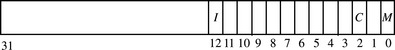
To enable the MPU, caches, and write buffer requires modifying bit values in CP15:c1:c0:0, the system control register. The location of the MPU, cache, and write buffer bits in CP15:c1:c0 are the same in the ARM940T, ARM946E-S, and ARM1026EJ-S processors, which makes enabling a configured MPU the same for the three cores. The enable bit locations are shown in Figure 13.6 and Table 13.9. The CP15:c1:c0 register has configuration bits not shown in Figure 13.6; the purpose and location of these bits are processor specific and are not a part of the protection system.
Table 13.9
Protection unit enable bits in CP15 control register 1.
| Bit | Function enabled | Value |
| 0 | MPU | 0 = disabled, 1 = enabled |
| 2 | data cache | 0 = disabled, 1 = enabled |
| 12 | instruction cache | 0 = disabled, 1 = enabled |
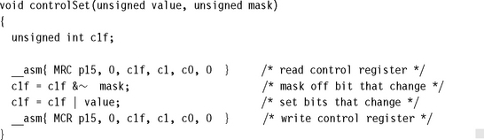
We use the routine changeControl, shown in Example 13.5, to enable the MPU and caches. However, the routine changeControl can change any set of values in the CP15:c1:c0:0 register. It has the following C function prototype:
![]()
The first parameter passed is an unsigned integer containing the bit values to change. The second parameter is used to select the bits you want changed: A bit value of 1 changes the bit in the control register, and a 0 leaves the bit value unchanged, regardless of the bit state in the first parameter.
For example, to enable the MPU and I-cache, and disable the D-cache, set bit [12] to 1, bit [2] to 0, and bit [0] to 1. The value of the first parameter should be 0×00001001; the remaining unchanged bits should be zero. To select only bit [12], bit [2], and bit [0] as the values to change, set the mask value to 0×00001005.
13.3 DEMONSTRATION OF AN MPU SYSTEM
We have provided a set of routines to use as building blocks to initialize and control a protected system. This section uses the routines described to initialize and control a simple protected system using a fixed memory map.
Here is a demonstration that uses the examples presented in the previous sections of this chapter to create a functional protection system. It provides an infrastructure that enables the running of three tasks in a simple protected multi-tasking system. We believe it provides a suitable demonstration of the concepts underlying the ARM MPU hardware. It is written in C and uses standard access permission.
13.3.1 SYSTEM REQUIREMENTS
The demonstration system has the following hardware characteristics:
![]() 256 KB of physical memory starting at 0×0 and ending at 0×40000
256 KB of physical memory starting at 0×0 and ending at 0×40000
![]() Several memory-mapped peripherals spaced over several megabytes from 0×10000000 to 0×12000000
Several memory-mapped peripherals spaced over several megabytes from 0×10000000 to 0×12000000
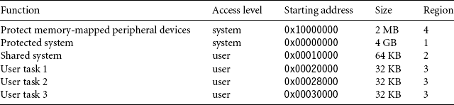
In this demonstration, all the memory-mapped peripherals are considered a single area of memory that needs protection (see Table 13.10).
The demonstration system has the following software components:
![]() The system software is less than 64 KB in size. It includes the vector table, exception handlers, and data stacks to support the exceptions. The system software must be inaccessible from user mode; that is, a user mode task must make a system call to run code or access data in this region.
The system software is less than 64 KB in size. It includes the vector table, exception handlers, and data stacks to support the exceptions. The system software must be inaccessible from user mode; that is, a user mode task must make a system call to run code or access data in this region.
![]() There is shared software that is less than 64 KB in size. It contains commonly used libraries and data space for messaging between user tasks.
There is shared software that is less than 64 KB in size. It contains commonly used libraries and data space for messaging between user tasks.
![]() There are three user tasks that control independent functions in the system. These tasks are less than 32 KB in size. When these tasks are running, they must be protected from access by the other two tasks.
There are three user tasks that control independent functions in the system. These tasks are less than 32 KB in size. When these tasks are running, they must be protected from access by the other two tasks.
The software is linked to place the software components within the regions assigned to them. Table 13.10 shows the software memory map for the example. The system software has system-level access permission. The shared software area is accessible by the entire system. The task software areas contain user-level tasks.
13.3.2 ASSIGNING REGIONS USING A MEMORY MAP
The last column of Table 13.10 shows the four regions we assigned to the memory areas. The regions are defined using the starting address listed in the table and the size of the code and data blocks. A memory map showing the region layout is provided in Figure 13.7.
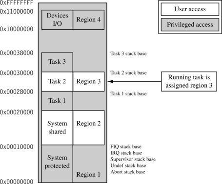
Region 1 is a background region that covers the entire addressable memory space. It is a privileged region (i.e., no user mode access is permitted). The instruction cache is enabled, and the data cache operates with a writethrough policy. This region has the lowest region priority because it is the region with the lowest assigned number.
The primary function of region 1 is to restrict access to the 64 KB space between 0×0 and 0×10000, the protected system area. Region 1 has two secondary functions: it acts as a background region and as a protection region for dormant user tasks. As a background region it ensures the entire memory space by default is assigned system-level access; this is done to prevent a user task from accessing spare or unused memory locations. As a user task protection region, it protects dormant tasks from misconduct by the running task (see Figure 13.7).
Region 2 controls access to shared system resources. It has a starting address of 0×10000 and is 64 KB in length. It maps directly over the shared memory space of the shared system code. Region 2 lies on top of a portion of protected region 1 and will take precedence over protected region 1 because it has a higher region number. Region 2 permits both user and system level memory access.
Region 3 controls the memory area and attributes of a running task. When control transfers from one task to another, as during a context switch, the operating system redefines region 3 so that it overlays the memory area of the running task. When region 3 is relocated over the new task, it exposes the previous task to the attributes of region 1. The previous task becomes part of region 1, and the running task is a new region 3. The running task cannot access the previous task because it is protected by the attributes of region 1.
Region 4 is the memory-mapped peripheral system space. The primary purpose of this region is to establish the area as not cached and not buffered. We don’t want input, output, or control registers subject to the stale data issues caused by caching, or the time or sequence issues involved when using buffered writes (see Chapter 12 for details on using I/O devices with caches and write buffers).
13.3.3 INITIALIZING THE MPU
To organize the initialization process we created a datatype called Region; it is a structure whose members hold the attributes of a region used during system operation. This Region structure is not required when using the MPU; it is simply a design convenience created to support the demonstration software. For this demonstration, we call the set of these data structures a region control block (RCB).
The initialization software uses the information stored in the RCB to configure the regions in the MPU. Note that there can be more Region structures defined in the RCB than physical regions. For example, region 3 is the only region used for tasks, yet there are three Region structures that use region 3, one for each user task. The typedef for the structure is
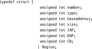
There are eight values in the Region structure. The first two values describe characteristics of the Region itself: they are the MPU region number assigned to the Region, and the type of access permission used, either STANDARD or EXTENDED. The remaining four members of the structure are attributes of the specified region: the region starting address, baseaddress; region size, SIZE; access permissions, IAP and DAP; and cache and buffer configuration, CB.
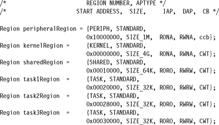
The six Region structures in the RCB are
We created a set of macros to make entries in the RCB more humanly readable; they are shown in Figure 13.8. Most notably, we enter access permission to data and instruction memory using a simple combination of four letters. The first two letters represent system access permission, and the second two letters represent user access. The two letters for system and user access can be read/write (RW), read-only (RO), or no access (NA).
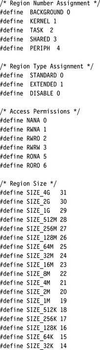
We also mapped the cache and buffer information to an instruction cache and a data cache policy attribute. The first letter is C or c and enables or disables the instruction cache for the region. The last two letters determine the data cache policy and write buffer control. The values can be WT for writethrough or WB for writeback. The letters c and b are also supported and are manual configurations of the cache and buffer bits. Cb is an alias of WT, and CB is an alias of WB. cB means not cached and buffered, and finally cb means not cached and not buffered.
13.3.4 INITIALIZING AND CONFIGURING A REGION
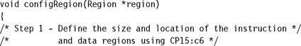
Next we provide the routine configRegion, which takes a single Region structure entry in the RCB to populate the CP15 registers with data describing the region.
The routine follows the initialization steps listed in Section 13.3.3. The input to the routine is a pointer to the RCB of a region. Within the routine, members of the Region are used as data inputs in the initialization process. The routine has the following C function prototype:
![]()
EXAMPLE 13.6
This example initializes the MPU, caches, and write buffer for the protected system. The routines presented earlier in this chapter are used in the initialization process. We implement the steps first listed in Section 13.2 to initialize the MPU, caches, and write buffer. The steps are labeled as comments in the example code. Executing this example initializes the MPU.
13.3.5 PUTTING IT ALL TOGETHER, INITIALIZING THE MPU
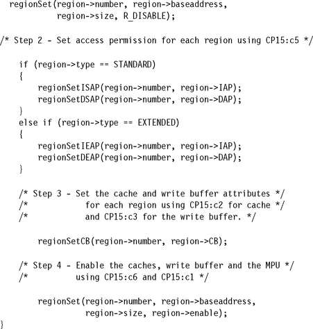
For the demonstration, we use the RCB to store data describing all regions. To initialize the MPU we use a top-level routine named initActiveRegions. The routine is called once for each active region when the system starts up. To complete the initialization, the routine also enables the MPU. The routine has the following C function prototype:
![]()
The routine has no input parameters.
EXAMPLE 13.7
The routine first calls configRegion once for each region that is active at system startup: the kernelRegion, the sharedRegion, the peripheralRegion, and the task1Region. In this demonstration task 1 is the first task entered. The last routine called is controlSet, which enables the caches and MPU.
13.3.6 A PROTECTED CONTEXT SWITCH
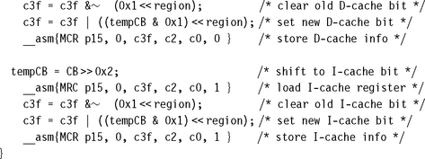
The demonstration system is now initialized, and the control system has launched its first task. At some point, the system will make a context switch to run another task. The RCB contains the current task’s region context information, so there is no need to save region data from the CP15 registers during the context switch.
To switch to the next task, for example task 2, the operating system would move region 3 over the task 2 memory area (see Figure 13.7). We reuse the routine configRegion to perform this function as part of the setup just prior to executing the code that performs the context switch between the current task and the next task. The input to configRegion would be a pointer to the task2Region. See the following assembly code sample:
![]()
![]()
13.3.7 MPUSLOS
Many of the concepts and the code examples have been incorporated into a functional control system we call mpuSLOS.
mpuSLOS is the memory protection unit variant of SLOS that was described in Chapter 11. It can be found on the publisher’s Web site and implements the same functions as the base SLOS with a number of important differences.
![]() mpuSLOS takes full advantage of the MPU.
mpuSLOS takes full advantage of the MPU.
![]() Applications are compiled and built separately from the kernel and then combined as a single binary file. Each application is linked to execute out of a different memory area.
Applications are compiled and built separately from the kernel and then combined as a single binary file. Each application is linked to execute out of a different memory area.
![]() Each of the three applications are loaded into separate fixed regions 32 KB in size by a routine called the Static Application Loader. This address is the execution address of the application. The stack pointer is set at the top of the 32 KB since each region is 32 KB in size.
Each of the three applications are loaded into separate fixed regions 32 KB in size by a routine called the Static Application Loader. This address is the execution address of the application. The stack pointer is set at the top of the 32 KB since each region is 32 KB in size.
![]() Applications can only access hardware via a device driver call. If an application attempts to access hardware directly, a data abort is raised. This differs from the base SLOS variant since a data abort will not be raised when a device is accessed directly from an application.
Applications can only access hardware via a device driver call. If an application attempts to access hardware directly, a data abort is raised. This differs from the base SLOS variant since a data abort will not be raised when a device is accessed directly from an application.
![]() Jumping to an application involves setting up the spsr and then changing the pc to point to the entry point to task 1 using a MOVS instruction.
Jumping to an application involves setting up the spsr and then changing the pc to point to the entry point to task 1 using a MOVS instruction.
![]() Each time the scheduler is called, the active region 2 is changed to reflect the new executing application.
Each time the scheduler is called, the active region 2 is changed to reflect the new executing application.
13.4 SUMMARY
There are two methods to handle memory protection. The first method is known as unprotected and uses voluntarily enforced software control routines to manage rules for task interaction. The second method is known as protected and uses hardware and software to enforce rules for task interaction. In a protected system the hardware protects areas of memory by generating an abort when access permission is violated and software responds to handle the abort routines and manage control to memory-based resources.
An ARM MPU uses regions as the primary construct for system protection. A region is a set of attributes associated with an area of memory. Regions can overlap, allowing the use of a background region to shield a dormant task’s memory areas from unwanted access by the current running task.
Several steps are required to initialize the MPU, included are routines to set various region attributes. The first step sets the size and location of the instruction and data regions using CP15:c6. The second step sets the access permission for each region using CP15:c5. The third step sets the cache and write buffer attributes for each region using CP15:c2 for cache and CP15:c3 for the write buffer. The last step enables active regions using CP15:c6 and the caches, write buffer, and MPU using CP15:c1.
In closing, a demonstration system showed three tasks, each protected from the other, in a simple multitasking environment. The demonstration system defined a protected system and then showed how to initialize it. After initialization, the last step needed to run a protected system is to change the region assignments to the next task during a task switch. This demonstration system is incorporated into mpuSLOS to provide a functional example of a protected operating system.