
CACHES
12.1. THE MEMORY HIERARCHY AND CACHE MEMORY
12.2.1. Basic Architecture of a Cache Memory
12.2.2. Basic Operation of a Cache Controller
12.4. COPROCESSOR 15 AND CACHES
12.5. FLUSHING AND CLEANING CACHE MEMORY
12.5.1. Flushing ARM Cached Cores
12.5.2. Cleaning ARM Cached Cores
12.5.4. Cleaning the D-Cache Using Way and Set Index Addressing
12.5.5. Cleaning the D-Cache Using the Test-Clean Command
12.5.6. Cleaning the D-Cache in Intel XScale SA-110 and Intel StrongARM Cores
12.6.1. Locking Code and Data in Cache
12.6.2. Locking a Cache by Incrementing the Way Index
A cache is a small, fast array of memory placed between the processor core and main memory that stores portions of recently referenced main memory. The processor uses cache memory instead of main memory whenever possible to increase system performance. The goal of a cache is to reduce the memory access bottleneck imposed on the processor core by slow memory.
Often used with a cache is a write buffer—a very small first-in-first-out (FIFO) memory placed between the processor core and main memory. The purpose of a write buffer is to free the processor core and cache memory from the slow write time associated with writing to main memory.
The word cache is a French word meaning “a concealed place for storage.” When applied to ARM embedded systems, this definition is very accurate. The cache memory and write buffer hardware when added to a processor core are designed to be transparent to software code execution, and thus previously written software does not need to be rewritten for use on a cached core. Both the cache and write buffer have additional control hardware that automatically handles the movement of code and data between the processor and main memory. However, knowing the details of a processor’s cache design can help you create programs that run faster on a specific ARM core.
Since the majority of this chapter is about the wonderful things a cache can do to make programs run faster, the question arises, “Are there any drawbacks created by having a cache in your system?” The answer is yes. The main drawback is the difficulty of determining the execution time of a program. Why this is a problem will become evident shortly.
Since cache memory only represents a very small portion of main memory, the cache fills quickly during program execution. Once full, the cache controller frequently evicts existing code or data from cache memory to make more room for the new code or data. This eviction process tends to occur randomly, leaving some data in cache and removing others. Thus, at any given instant in time, a value may or may not be stored in cache memory.
Because data may or may not be present in cache at any given point in time, the execution time of a routine may vary slightly from run to run due to the difference between the time it takes to use data immediately out of cache memory and the time it takes to load a cache line from main memory.
So, with that caveat, we begin by showing where caches fit in a standard memory hierarchy and introduce the principle of locality of reference to explain why a cache improves system performance. We then describe cache architectures in general and define a set of terms used by the ARM community. We end the chapter with example code showing how to clean and flush caches and to lock code and data segments in cache.
12.1 THE MEMORY HIERARCHY AND CACHE MEMORY
In Chapter 1 we introduced the memory hierarchy in a computer system. Figure 12.1 reviews some of this information to show where a cache and write buffer fit in the hierarchy.
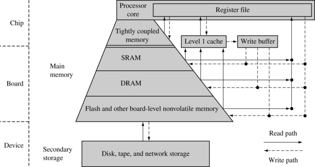
The innermost level of the hierarchy is at the processor core. This memory is so tightly coupled to the processor that in many ways it is difficult to think of it as separate from the processor. This memory is known as a register file. These registers are integral to the processor core and provide the fastest possible memory access in the system.
At the primary level, memory components are connected to the processor core through dedicated on-chip interfaces. It is at this level we find tightly coupled memory (TCM) and level 1 cache. We talk more about caches in a moment.
Also at the primary level is main memory. It includes volatile components like SRAM and DRAM, and nonvolatile components like flash memory. The purpose of main memory is to hold programs while they are running on a system.
The next level is secondary storage—large, slow, relatively inexpensive mass storage devices such as disk drives or removable memory. Also included in this level is data derived from peripheral devices, which are characterized by their extremely long access times. Secondary memory is used to store unused portions of very large programs that do not fit in main memory and programs that are not currently executing.
It is useful to note that a memory hierarchy depends as much on architectural design as on the technology surrounding it. For example, TCM and SRAM are of the same technology yet differ in architectural placement: TCM is located on the chip, while SRAM is located on a board.
A cache may be incorporated between any level in the hierarchy where there is a significant access time difference between memory components. A cache can improve system performance whenever such a difference exists. A cache memory system takes information stored in a lower level of the hierarchy and temporarily moves it to a higher level.
Figure 12.1 includes a level 1 (L1) cache and write buffer. The L1 cache is an array of high-speed, on-chip memory that temporarily holds code and data from a slower level. A cache holds this information to decrease the time required to access both instructions and data. The write buffer is a very small FIFO buffer that supports writes to main memory from the cache.
Not shown in the figure is a level 2 (L2) cache. An L2 cache is located between the L1 cache and slower memory. The L1 and L2 caches are also known as the primary and secondary caches.
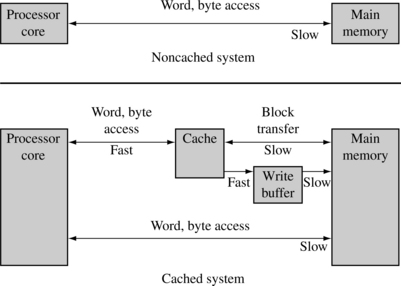
Figure 12.2 shows the relationship that a cache has with main memory system and the processor core. The upper half of the figure shows a block diagram of a system without a cache. Main memory is accessed directly by the processor core using the datatypes supported by the processor core. The lower half of the diagram shows a system with a cache. The cache memory is much faster than main memory and thus responds quickly to data requests by the core. The cache’s relationship with main memory involves the transfer of small blocks of data between the slower main memory to the faster cache memory. These blocks of data are known as cache lines. The write buffer acts as a temporary buffer that frees available space in the cache memory. The cache transfers a cache line to the write buffer at high speed and then the write buffer drains it to main memory at slow speed.
12.1.1 CACHES AND MEMORY MANAGEMENT UNITS
If a cached core supports virtual memory, it can be located between the core and the memory management unit (MMU), or between the MMU and physical memory. Placement of the cache before or after the MMU determines the addressing realm the cache operates in and how a programmer views the cache memory system. Figure 12.3 shows the difference between the two caches.
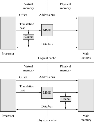
A logical cache stores data in a virtual address space. A logical cache is located between the processor and the MMU. The processor can access data from a logical cache directly without going through the MMU. A logical cache is also known as a virtual cache.
A physical cache stores memory using physical addresses. A physical cache is located between the MMU and main memory. For the processor to access memory, the MMU must first translate the virtual address to a physical address before the cache memory can provide data to the core.
ARM cached cores with an MMU use logical caches for processor families ARM7 through ARM10, including the Intel StrongARM and Intel XScale processors. The ARM11 processor family uses a physical cache. See Chapter 14 for additional information on the operation of the MMU.
The improvement a cache provides is possible because computer programs execute in nonrandom ways. Predictable program execution is the key to the success of cached systems. If a program’s accesses to memory were random, a cache would provide little improvement to overall system performance. The principle of locality of reference explains the performance improvement provided by the addition of a cache memory to a system. This principle states that computer software programs frequently run small loops of code that repeatedly operate on local sections of data memory.
The repeated use of the same code or data in memory, or those very near, is the reason a cache improves performance. By loading the referenced code or data into faster memory when first accessed, each subsequent access will be much faster. It is the repeated access to the faster memory that improves performance.
The cache makes use of this repeated local reference in both time and space. If the reference is in time, it is called temporal locality. If it is by address proximity, then it is called spatial locality.
12.2 CACHE ARCHITECTURE
ARM uses two bus architectures in its cached cores, the Von Neumann and the Harvard. The Von Neumann and Harvard bus architectures differ in the separation of the instruction and data paths between the core and memory. A different cache design is used to support the two architectures.
In processor cores using the Von Neumann architecture, there is a single cache used for instruction and data. This type of cache is known as a unified cache. A unified cache memory contains both instruction and data values.
The Harvard architecture has separate instruction and data buses to improve overall system performance, but supporting the two buses requires two caches. In processor cores using the Harvard architecture, there are two caches: an instruction cache (I-cache) and a data cache (D-cache). This type of cache is known as a split cache. In a split cache, instructions are stored in the instruction cache and data values are stored in the data cache.
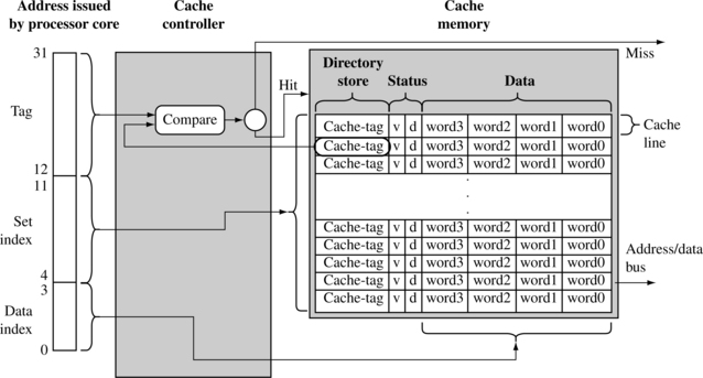
We introduce the basic architecture of caches by showing a unified cache in Figure 12.4. The two main elements of a cache are the cache controller and the cache memory. The cache memory is a dedicated memory array accessed in units called cache lines. The cache controller uses different portions of the address issued by the processor during a memory request to select parts of cache memory. We will present the architecture of the cache memory first and then proceed to the details of the cache controller.
12.2.1 BASIC ARCHITECTURE OF A CACHE MEMORY
A simple cache memory is shown on the right side of Figure 12.4. It has three main parts: a directory store, a data section, and status information. All three parts of the cache memory are present for each cache line.
The cache must know where the information stored in a cache line originates from in main memory. It uses a directory store to hold the address identifying where the cache line was copied from main memory. The directory entry is known as a cache-tag.
A cache memory must also store the data read from main memory. This information is held in the data section (see Figure 12.4).
The size of a cache is defined as the actual code or data the cache can store from main memory. Not included in the cache size is the cache memory required to support cache-tags or status bits.
There are also status bits in cache memory to maintain state information. Two common status bits are the valid bit and dirty bit. A valid bit marks a cache line as active, meaning it contains live data originally taken from main memory and is currently available to the processor core on demand. A dirty bit defines whether or not a cache line contains data that is different from the value it represents in main memory. We explain dirty bits in more detail in Section 12.3.1.
12.2.2 BASIC OPERATION OF A CACHE CONTROLLER
The cache controller is hardware that copies code or data from main memory to cache memory automatically. It performs this task automatically to conceal cache operation from the software it supports. Thus, the same application software can run unaltered on systems with and without a cache.
The cache controller intercepts read and write memory requests before passing them on to the memory controller. It processes a request by dividing the address of the request into three fields, the tag field, the set index field, and the data index field. The three bit fields are shown in Figure 12.4.
First, the controller uses the set index portion of the address to locate the cache line within the cache memory that might hold the requested code or data. This cache line contains the cache-tag and status bits, which the controller uses to determine the actual data stored there.
The controller then checks the valid bit to determine if the cache line is active, and compares the cache-tag to the tag field of the requested address. If both the status check and comparison succeed, it is a cache hit. If either the status check or comparison fails, it is a cache miss.
On a cache miss, the controller copies an entire cache line from main memory to cache memory and provides the requested code or data to the processor. The copying of a cache line from main memory to cache memory is known as a cache line fill.
On a cache hit, the controller supplies the code or data directly from cache memory to the processor. To do this it moves to the next step, which is to use the data index field of the address request to select the actual code or data in the cache line and provide it to the processor.
12.2.3 THE RELATIONSHIP BETWEEN CACHE AND MAIN MEMORY
Having a general understanding of basic cache memory architecture and how the cache controller works provides enough information to discuss the relationship that a cache has with main memory.
Figure 12.5 shows where portions of main memory are temporarily stored in cache memory. The figure represents the simplest form of cache, known as a direct-mapped cache. In a direct-mapped cache each addressed location in main memory maps to a single location in cache memory. Since main memory is much larger than cache memory, there are many addresses in main memory that map to the same single location in cache memory. The figure shows this relationship for the class of addresses ending in 0x824.
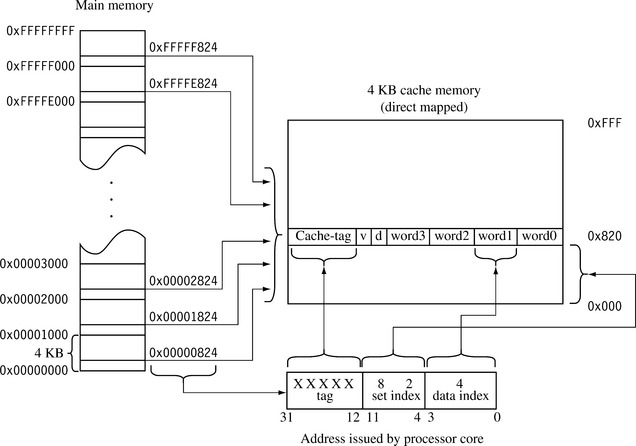
The three bit fields introduced in Figure 12.4 are also shown in this figure. The set index selects the one location in cache where all values in memory with an ending address of 0x824 are stored. The data index selects the word/halfword/byte in the cache line, in this case the second word in the cache line. The tag field is the portion of the address that is compared to the cache-tag value found in the directory store. In this example there are one million possible locations in main memory for every one location in cache memory. Only one of the possible one million values in the main memory can exist in the cache memory at any given time. The comparison of the tag with the cache-tag determines whether the requested data is in cache or represents another of the million locations in main memory with an ending address of 0x824.
During a cache line fill the cache controller may forward the loading data to the core at the same time it is copying it to cache; this is known as data streaming. Streaming allows a processor to continue execution while the cache controller fills the remaining words in the cache line.
If valid data exists in this cache line but represents another address block in main memory, the entire cache line is evicted and replaced by the cache line containing the requested address. This process of removing an existing cache line as part of servicing a cache miss is known as eviction—returning the contents of a cache line to main memory from the cache to make room for new data that needs to be loaded in cache.
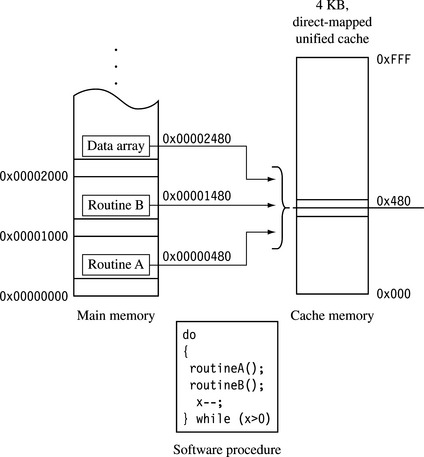
A direct-mapped cache is a simple solution, but there is a design cost inherent in having a single location available to store a value from main memory. Direct-mapped caches are subject to high levels of thrashing—a software battle for the same location in cache memory. The result of thrashing is the repeated loading and eviction of a cache line. The loading and eviction result from program elements being placed in main memory at addresses that map to the same cache line in cache memory.
Figure 12.6 takes Figure 12.5 and overlays a simple, contrived software procedure to demonstrate thrashing. The procedure calls two routines repeatedly in a do while loop. Each routine has the same set index address; that is, the routines are found at addresses in physical memory that map to the same location in cache memory. The first time through the loop, routine A is placed in the cache as it executes. When the procedure calls routine B, it evicts routine A a cache line at a time as it is loaded into cache and executed. On the second time through the loop, routine A replaces routine B, and then routine B replaces routine A. Repeated cache misses result in continuous eviction of the routine that not running. This is cache thrashing.
12.2.4 SET ASSOCIATIVITY
Some caches include an additional design feature to reduce the frequency of thrashing (see Figure 12.7). This structural design feature is a change that divides the cache memory into smaller equal units, called ways. Figure 12.7 is still a four KB cache; however, the set index now addresses more than one cache line—it points to one cache line in each way. Instead of one way of 256 lines, the cache has four ways of 64 lines. The four cache lines with the same set index are said to be in the same set, which is the origin of the name “set index.”
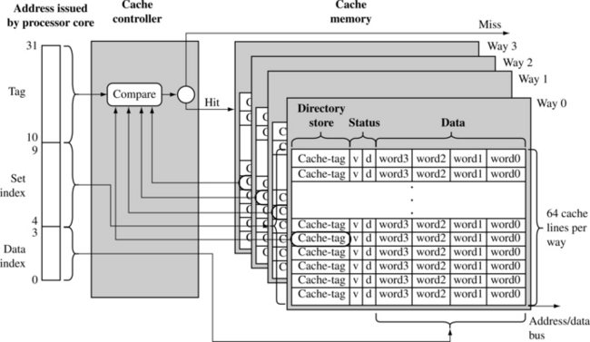
Figure 12.7 A 4 KB, four-way set associative cache. The cache has 256 total cache lines, which are separated into four ways, each containing 64 cache lines. The cache line contains four words.
The set of cache lines pointed to by the set index are set associative. A data or code block from main memory can be allocated to any of the four ways in a set without affecting program behavior; in other words the storing of data in cache lines within a set does not affect program execution. Two sequential blocks from main memory can be stored as cache lines in the same way or two different ways. The important thing to note is that the data or code blocks from a specific location in main memory can be stored in any cache line that is a member of a set. The placement of values within a set is exclusive to prevent the same code or data block from simultaneously occupying two cache lines in a set.
The mapping of main memory to a cache changes in a four-way set associative cache. Figure 12.8 shows the differences. Any single location in main memory now maps to four different locations in the cache. Although Figures 12.5 and 12.8 both illustrate 4 KB caches, here are some differences worth noting.
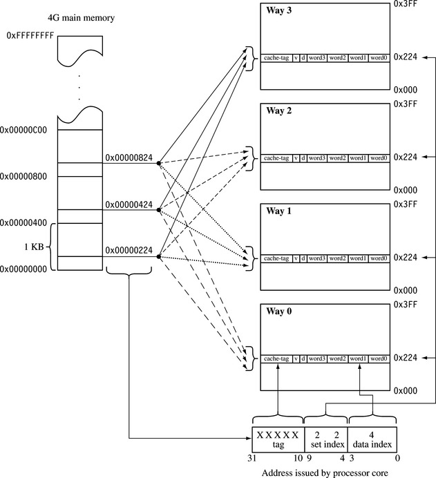
The bit field for the tag is now two bits larger, and the set index bit field is two bits smaller. This means four million main memory addresses now map to one set of four cache lines, instead of one million addresses mapping to one location.
The size of the area of main memory that maps to cache is now 1 KB instead of 4 KB. This means that the likelihood of mapping cache line data blocks to the same set is now four times higher. This is offset by the fact that a cache line is one fourth less likely to be evicted.
If the example code shown in Figure 12.6 were run in the four-way set associative cache shown in Figure 12.8, the incidence of thrashing would quickly settle down as routine A, routine B, and the data array would establish unique places in the four available locations in a set. This assumes that the size of each routine and the data are less than the new smaller 1 KB area that maps from main memory.
12.2.4.1 Increasing Set Associativity
As the associativity of a cache controller goes up, the probability of thrashing goes down. The ideal goal would be to maximize the set associativity of a cache by designing it so any main memory location maps to any cache line. A cache that does this is known as a fully associative cache. However, as the associativity increases, so does the complexity of the hardware that supports it. One method used by hardware designers to increase the set associativity of a cache includes a content addressable memory (CAM).
A CAM uses a set of comparators to compare the input tag address with a cache-tag stored in each valid cache line. A CAM works in the opposite way a RAM works. Where a RAM produces data when given an address value, a CAM produces an address if a given data value exists in the memory. Using a CAM allows many more cache-tags to be compared simultaneously, thereby increasing the number of cache lines that can be included in a set.
Using a CAM to locate cache-tags is the design choice ARM made in their ARM920T and ARM940T processor cores. The caches in the ARM920T and ARM940T are 64-way set associative. Figure 12.9 shows a block diagram of an ARM940T cache. The cache controller uses the address tag as the input to the CAM and the output selects the way containing the valid cache line.
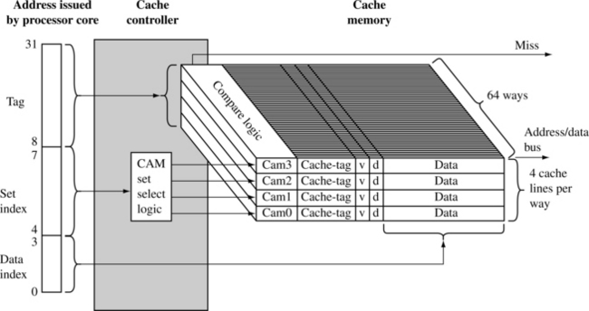
The tag portion of the requested address is used as an input to the four CAMs that simultaneously compare the input tag with all cache-tags stored in the 64 ways. If there is a match, cache data is provided by the cache memory. If no match occurs, a miss signal is generated by the memory controller.
The controller enables one of four CAMs using the set index bits. The indexed CAM then selects a cache line in cache memory and the data index portion of the core address selects the requested word, halfword, or byte within the cache line.
12.2.5 WRITE BUFFERS
A write buffer is a very small, fast FIFO memory buffer that temporarily holds data that the processor would normally write to main memory. In a system without a write buffer, the processor writes directly to main memory. In a system with a write buffer, data is written at high speed to the FIFO and then emptied to slower main memory. The write buffer reduces the processor time taken to write small blocks of sequential data to main memory. The FIFO memory of the write buffer is at the same level in the memory hierarchy as the L1 cache and is shown in Figure 12.1.
The efficiency of the write buffer depends on the ratio of main memory writes to the number of instructions executed. Over a given time interval, if the number of writes to main memory is low or sufficiently spaced between other processing instructions, the write buffer will rarely fill. If the write buffer does not fill, the running program continues to execute out of cache memory using registers for processing, cache memory for reads and writes, and the write buffer for holding evicted cache lines while they drain to main memory.
A write buffer also improves cache performance; the improvement occurs during cache line evictions. If the cache controller evicts a dirty cache line, it writes the cache line to the write buffer instead of main memory. Thus the new cache line data will be available sooner, and the processor can continue operating from cache memory.
Data written to the write buffer is not available for reading until it has exited the write buffer to main memory. The same holds true for an evicted cache line: it too cannot be read while it is in the write buffer. This is one of the reasons that the FIFO depth of a write buffer is usually quite small, only a few cache lines deep.
Some write buffers are not strictly FIFO buffers. The ARM10 family, for example, supports coalescing—the merging of write operations into a single cache line. The write buffer will merge the new value into an existing cache line in the write buffer if they represent the same data block in main memory. Coalescing is also known as write merging, write collapsing, or write combining.
12.2.6 MEASURING CACHE EFFICIENCY
There are two terms used to characterize the cache efficiency of a program: the cache hit rate and the cache miss rate. The hit rate is the number of cache hits divided by the total number of memory requests over a given time interval. The value is expressed as a percentage:
The miss rate is similar in form: the total cache misses divided by the total number of memory requests expressed as a percentage over a time interval. Note that the miss rate also equals 100 minus the hit rate.
The hit rate and miss rate can measure reads, writes, or both, which means that the terms can be used to describe performance information in several ways. For example, there is a hit rate for reads, a hit rate for writes, and other measures of hit and miss rates.
Two other terms used in cache performance measurement are the hit time—the time it takes to access a memory location in the cache and the miss penalty—the time it takes to load a cache line from main memory into cache.
12.3 CACHE POLICY
There are three policies that determine the operation of a cache: the write policy, the replacement policy, and the allocation policy. The cache write policy determines where data is stored during processor write operations. The replacement policy selects the cache line in a set that is used for the next line fill during a cache miss. The allocation policy determines when the cache controller allocates a cache line.
12.3.1 WRITE POLICY—WRITEBACK OR WRITETHROUGH
When the processor core writes to memory, the cache controller has two alternatives for its write policy. The controller can write to both the cache and main memory, updating the values in both locations; this approach is known as writethrough. Alternatively, the cache controller can write to cache memory and not update main memory, this is known as writeback or copyback.
12.3.1.1 Writethrough
When the cache controller uses a writethrough policy, it writes to both cache and main memory when there is a cache hit on write, ensuring that the cache and main memory stay coherent at all times. Under this policy, the cache controller performs a write to main memory for each write to cache memory. Because of the write to main memory, a writethrough policy is slower than a writeback policy.
12.3.1.2 Writeback
When a cache controller uses a writeback policy, it writes to valid cache data memory and not to main memory. Consequently, valid cache lines and main memory may contain different data. The cache line holds the most recent data, and main memory contains older data, which has not been updated.
Caches configured as writeback caches must use one or more of the dirty bits in the cache line status information block. When a cache controller in writeback writes a value to cache memory, it sets the dirty bit true. If the core accesses the cache line at a later time, it knows by the state of the dirty bit that the cache line contains data not in main memory. If the cache controller evicts a dirty cache line, it is automatically written out to main memory. The controller does this to prevent the loss of vital information held in cache memory and not in main memory.
One performance advantage a writeback cache has over a writethrough cache is in the frequent use of temporary local variables by a subroutine. These variables are transient in nature and never really need to be written to main memory. An example of one of these transient variables is a local variable that overflows onto a cached stack because there are not enough registers in the register file to hold the variable.
12.3.2 CACHE LINE REPLACEMENT POLICIES
On a cache miss, the cache controller must select a cache line from the available set in cache memory to store the new information from main memory. The cache line selected for replacement is known as a victim. If the victim contains valid, dirty data, the controller must write the dirty data from the cache memory to main memory before it copies new data into the victim cache line. The process of selecting and replacing a victim cache line is known as eviction.
The strategy implemented in a cache controller to select the next victim is called its replacement policy. The replacement policy selects a cache line from the available associative member set; that is, it selects the way to use in the next cache line replacement. To summarize the overall process, the set index selects the set of cache lines available in the ways, and the replacement policy selects the specific cache line from the set to replace.
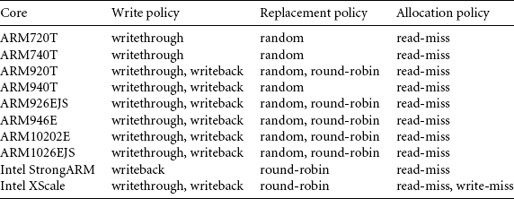
ARM cached cores support two replacement policies, either pseudorandom or round-robin.
![]() Round-robin or cyclic replacement simply selects the next cache line in a set to replace. The selection algorithm uses a sequential, incrementing victim counter that increments each time the cache controller allocates a cache line. When the victim counter reaches a maximum value, it is reset to a defined base value.
Round-robin or cyclic replacement simply selects the next cache line in a set to replace. The selection algorithm uses a sequential, incrementing victim counter that increments each time the cache controller allocates a cache line. When the victim counter reaches a maximum value, it is reset to a defined base value.
![]() Pseudorandom replacement randomly selects the next cache line in a set to replace. The selection algorithm uses a nonsequential incrementing victim counter. In a pseudorandom replacement algorithm the controller increments the victim counter by randomly selecting an increment value and adding this value to the victim counter. When the victim counter reaches a maximum value, it is reset to a defined base value.
Pseudorandom replacement randomly selects the next cache line in a set to replace. The selection algorithm uses a nonsequential incrementing victim counter. In a pseudorandom replacement algorithm the controller increments the victim counter by randomly selecting an increment value and adding this value to the victim counter. When the victim counter reaches a maximum value, it is reset to a defined base value.
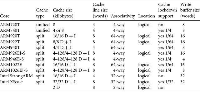
Most ARM cores support both policies (see Table 12.1 for a comprehensive list of ARM cores and the policies they support). The round-robin replacement policy has greater predictability, which is desirable in an embedded system. However, a round-robin replacement policy is subject to large changes in performance given small changes in memory access. To show this change in performance, we provide Example 12.1.
EXAMPLE 12.1
This example determines the time it takes to execute a software routine using the round-robin and random replacement policies. The test routine cache_RRtest collects timings using the clock function available in the C library header time.h. First, it enables a round robin policy and runs a timing test, and then enables the random policy and runs the same test.
The test routine readSet is written specifically for an ARM940T and intentionally shows a worst-case abrupt change in cache behavior using a round-robin replacement policy.
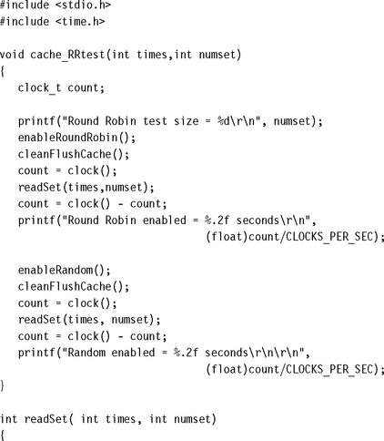
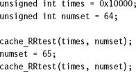
We wrote the readSet routine to fill a single set in the cache. There are two arguments to the function. The first, times, is the number of times to run the test loop; this value increases the time it takes to run the test. The second, numset, is the number of set values to read; this value determines the number of cache lines the routine loads into the same set. Filling the set with values is done in a loop using an LDR instruction that reads a value from a memory location and then increments the address by 16 words (64 bytes) in each pass through the loop. Setting the value of numset to 64 will fill all the available cache lines in a set in an ARM940T. There are 16 words in a way and 64 cache lines per set in the ARM940T.
Here are two calls to the round-robin test using two set sizes. The first reads and fills a set with 64 entries; the second attempts to fill the set with 65 entries.
The console output of the two tests follows. The tests were run on an ARM940T core module simulated using the ARM ADS1.2 ARMulator with a core clock speed of 50 MHz and a memory read access time of 100 ns nonsequential and 50 ns sequential. The thing to notice is the change in timing for the round-robin test reading 65 set values.
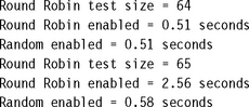
This is an extreme example, but it does shows a difference between using a round-robin policy and a random replacement policy.
Another common replacement policy is least recently used (LRU). This policy keeps track of cache line use and selects the cache line that has been unused for the longest time as the next victim.
ARM’s cached cores do not support a least recently used replacement policy, although ARM’s semiconductor partners have taken noncached ARM cores and added their own cache to the chips they produce. So there are ARM-based products that use an LRU replacement policy.
12.3.3 ALLOCATION POLICY ON A CACHE MISS
There are two strategies ARM caches may use to allocate a cache line after a the occurrence of a cache miss. The first strategy is known as read-allocate, and the second strategy is known as read-write-allocate.
A read allocate on cache miss policy allocates a cache line only during a read from main memory. If the victim cache line contains valid data, then it is written to main memory before the cache line is filled with new data.
Under this strategy, a write of new data to memory does not update the contents of the cache memory unless a cache line was allocated on a previous read from main memory. If the cache line contains valid data, then a write updates the cache and may update main memory if the cache write policy is writethrough. If the data is not in cache, the controller writes to main memory only.
A read-write allocate on cache miss policy allocates a cache line for either a read or write to memory. Any load or store operation made to main memory, which is not in cache memory, allocates a cache line. On memory reads the controller uses a read-allocate policy.
On a write, the controller also allocates a cache line. If the victim cache line contains valid data, then it is first written back to main memory before the cache controller fills the victim cache line with new data from main memory. If the cache line is not valid, it simply does a cache line fill. After the cache line is filled from main memory, the controller writes the data to the corresponding data location within the cache line. The cached core also updates main memory if it is a writethrough cache.
The ARM7, ARM9, and ARM10 cores use a read-allocate on miss policy; the Intel XScale supports both read-allocate and write-allocate on miss. Table 12.1 provides a listing of the policies supported by each core.
12.4 COPROCESSOR 15 AND CACHES
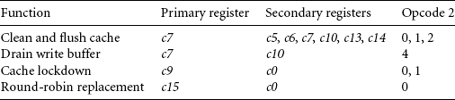
There are several coprocessor 15 registers used to specifically configure and control ARM cached cores. Table 12.2 lists the coprocessor 15 registers that control cache configuration. Primary CP15 registers c7 and c9 control the setup and operation of cache. Secondary CP15:c7 registers are write only and clean and flush cache. The CP15:c9 register defines the victim pointer base address, which determines the number of lines of code or data that are locked in cache. We discuss these commands in more detail in the sections that follow. To review the general use of coprocessor 15 instructions and syntax, see Section 3.5.2.
There are other CP15 registers that affect cache operation; the definition of these registers is core dependent. These other registers are explained in Chapter 13 in Sections 13.2.3 and 13.2.4 on initializing the MPU, and in Chapter 14 in Section 14.3.6 on initializing the MMU.
In the next several sections we use the CP15 registers listed in Table 12.2 to provide example routines to clean and flush caches, and to lock code or data in cache. The control system usually calls these routines as part of its memory management activities.
12.5 FLUSHING AND CLEANING CACHE MEMORY
ARM uses the terms flush and clean to describe two basic operations performed on a cache.
To “flush a cache” is to clear it of any stored data. Flushing simply clears the valid bit in the affected cache line. All or just portions of a cache may need flushing to support changes in memory configuration. The term invalidate is sometimes used in place of the term flush. However, if some portion of the D-cache is configured to use a writeback policy, the data cache may also need cleaning.
To “clean a cache” is to force a write of dirty cache lines from the cache out to main memory and clear the dirty bits in the cache line. Cleaning a cache reestablishes coherence between cached memory and main memory, and only applies to D-caches using a writeback policy.
Changing the memory configuration of a system may require cleaning or flushing a cache. The need to clean or flush a cache results directly from actions like changing the access permission, cache, and buffer policy, or remapping virtual addresses.
The cache may also need cleaning or flushing before the execution of self-modifying code in a split cache. Self-modifying code includes a simple copy of code from one location to another. The need to clean or flush arises from two possible conditions: First, the self-modifying code may be held in the D-cache and therefore be unavailable to load from main memory as an instruction. Second, existing instructions in the I-cache may mask new instructions written to main memory.
If a cache is using a writeback policy and self-modifying code is written to main memory, the first step is to write the instructions as a block of data to a location in main memory. At a later time, the program will branch to this memory and begin executing from that area of memory as an instruction stream. During the first write of code to main memory as data, it may be written to cache memory instead; this occurs in an ARM cache if valid cache lines exist in cache memory representing the location where the self-modifying code is written. The cache lines are copied to the D-cache and not to main memory. If this is the case, then when the program branches to the location where the self-modifying code should be, it will execute old instructions still present because the self-modifying code is still in the D-cache. To prevent this, clean the cache, which forces the instructions stored as data into main memory, where they can be read as an instruction stream.
If the D-cache has been cleaned, new instructions are present in main memory. However, the I-cache may have valid cache lines stored for the addresses where the new data (code) was written. Consequently, a fetch of the instruction at the address of the copied code would retrieve the old code from the I-cache and not the new code from main memory. Flush the I-cache to prevent this from happening.
12.5.1 FLUSHING ARM CACHED CORES
Flushing a cache invalidates the contents of a cache. If the cache is using a writeback policy, care should be taken to clean the cache before flushing so data is not lost as a result of the flushing process.
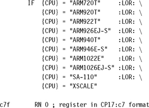
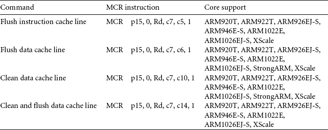
There are three CP15:c7 commands that perform flush operations on a cache. The first flushes the entire cache, the second flushes just the I-cache, and the third just the D-cache. The commands and cores that support them are shown in Table 12.3. The value of the processor core register Rd should be zero for all three MCR instructions.
Table 12.3
CP15:c7:Cm commands to flush the entire cache.
| Command | MCR instruction | Core support |
| Flush cache | MCR p15, 0, Rd, c7, c7, 0 | ARM720T, ARM920T, ARM922T, ARM926EJ-S, ARM1022E, ARM1026EJ-S, StrongARM, XScale |
| Flush data cache | MCR p15, 0, Rd, c7, c6, 0 | ARM920T, ARM922T, ARM926EJ-S, ARM940T, ARM946E-S, ARM1022E, ARM1026EJ-S, StrongARM, XScale |
| Flush instruction cache | MCR p15, 0, Rd, c7, c5, 0 | ARM920T, ARM922T, ARM926EJ-S, ARM940T, ARM946E-S, ARM1022E, ARM1026EJ-S, StrongARM, XScale |
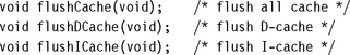
We provide Example 12.2 to show how to flush caches using these instructions. The example can be used “as is” or customized to suit the requirements of the system. The example contains a macro that produces three routines (for information on using macros, see Appendix A):
The routines have no input parameters and are called from C with the following prototypes:
EXAMPLE 12.2
This example begins by filtering the cores into groups based on the commands that they support.
We use a macro called CACHEFLUSH to help in the creation of the routines. The macro starts by setting the core register written to the CP15:c7:Cm to zero. Then it inserts the specific MCR instruction depending on the type of cache operation needed and its availability within each core.
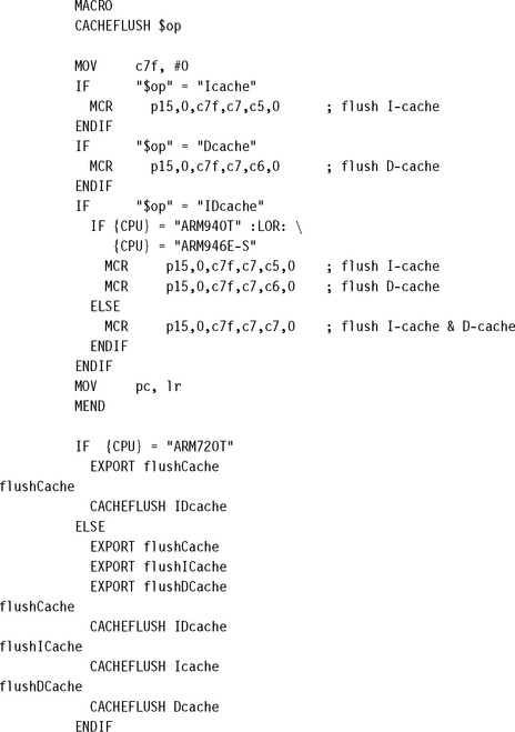
Finally, we use the macro several times to create the routines. The ARM720T has a unified cache so only the flushCache routine is available; otherwise, the routine uses the macro three times to create the routines.
This example contains a little more code than most implementations require. However, it is provided as an exhaustive routine that supports all current ARM processor cores.
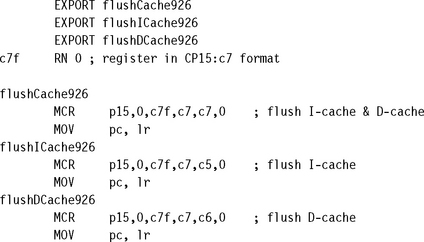
You can use Example 12.2 to create simpler routines dedicated to the specific core you are using. We use an ARM926EJ-S as a model to show how the three routines can be extracted from Example 12.2. The rewritten version is
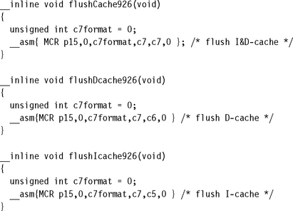
If you are writing in C, you might simplify this code even further and make them inline functions that can be collected and placed in an include file. The inline functions are
The remainder of the examples in this chapter are presented in ARM assembler and support all current cores. The same extraction procedures can be applied to the routines provided.
12.5.2 CLEANING ARM CACHED CORES
To clean a cache is to issue commands that force the cache controller to write all dirty D-cache lines out to main memory. In the process the dirty status bits in the cache line are cleared. Cleaning a cache reestablishes coherence between cached memory and main memory and can only apply to D-caches using a writeback policy.
The terms writeback and copyback are sometimes used in place of the term clean. So to force a writeback or copyback of cache to main memory is the same as cleaning the cache. The terms are similar to the adjectives used to describe cache write policy; however, in this case they describe an action performed on cache memory. In the non-ARM world the term flush may be used to mean what ARM calls clean.
12.5.3 CLEANING THE D-CACHE
At the time of writing this book there are three methods used to clean the D-cache (see Table 12.4); the method used is processor dependent because different cores have different command sets to clean the D-cache.
Table 12.4
Procedural methods to clean the D-cache.
| Method | Example | Processor |
| Way and set index addressing | Example 12.3 | ARM920T, ARM922T, ARM926EJ-S, ARM940T, ARM946E-S, ARM1022E, ARM1026EJ-S |
| Test-clean | Example 12.4 | ARM926EJ-S, ARM1026EJ-S |
| Special allocate command reading a dedicated block of memory | Example 12.5 | XScale, SA-110 |
Although the method used to clean the cache may vary, in the examples we provide the same procedure call to provide a consistent interface across all cores. To do this we provide the same three procedures to clean the entire cache written once for each method:
![]() cleanDCache cleans the entire D-cache.
cleanDCache cleans the entire D-cache.
![]() cleanFlushDCache cleans and flushes the entire D-cache.
cleanFlushDCache cleans and flushes the entire D-cache.
![]() cleanFlushCache cleans and flushes both the I-cache and D-cache.
cleanFlushCache cleans and flushes both the I-cache and D-cache.
The cleanDCache, cleanFlushDCache, and cleanFlushCache procedures do not take any input parameters and can be called from C using the following prototypes:
The macros in these examples were written to support as many ARM cores as possible without major modification. This effort produced a common header file used in this example and several other examples presented in this chapter. The header file is named cache.h and is shown in Figure 12.10.
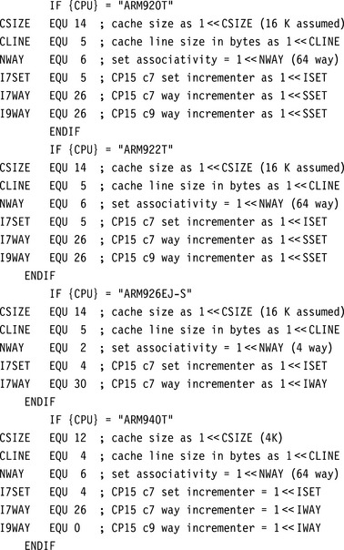
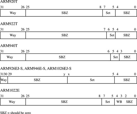
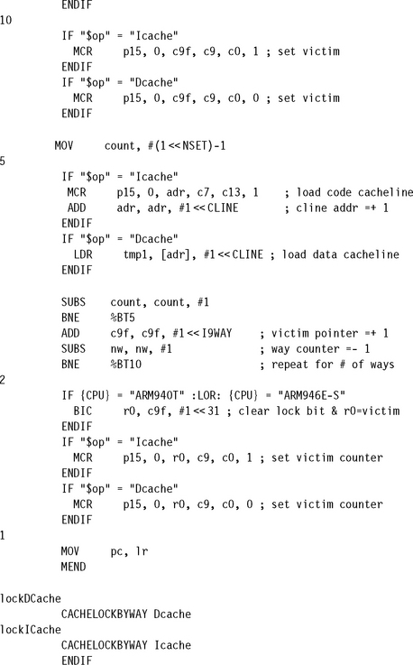
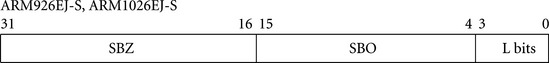
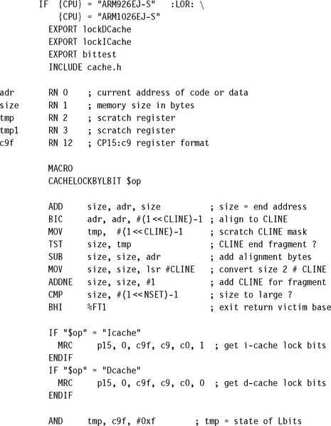
All values in the header file are either a size expressed in log base two or a field locator. If the value is a locator, it represents the lowest bit in a bit field in a CP15 register. For example, the constant I7WAY points to the lowest bit in the way selection field in the CP15:c7:c5 register. Just to be clear, the value of I7WAY is 26 in an ARM920T, ARM922T, ARM940T, and ARM1022E, and the value is 30 in the ARM926EJ-S, ARM946E-S, and ARM1026EJ-S (see Figure 12.11). The values are stored in this format to support bit manipulation of the core register (Rm) moved into a CP15:Cd:Cm register when a clean command is issued using an MCR instruction.
The six constants in the header file that depend on the core architecture are the following:
![]() CSIZE is the log base two of the size of the cache in bytes; in other words, the cache size is (1
CSIZE is the log base two of the size of the cache in bytes; in other words, the cache size is (1![]() CSIZE) bytes.
CSIZE) bytes.
![]() CLINE is the log base two of the length of a cache line in bytes; the cache line length would be (1
CLINE is the log base two of the length of a cache line in bytes; the cache line length would be (1![]() CLINE) bytes.
CLINE) bytes.
![]() NWAY is the number of ways and is the same as the set associativity.
NWAY is the number of ways and is the same as the set associativity.
![]() I7SET is the number of bits that the set index is shifted to the left in the CP15:c7 command register. This value is also used to increment or decrement the set index portion of the CP15:c7 register when sequentially accessing the cache.
I7SET is the number of bits that the set index is shifted to the left in the CP15:c7 command register. This value is also used to increment or decrement the set index portion of the CP15:c7 register when sequentially accessing the cache.
![]() I7WAY is the number of bits that the way index is shifted to the left in the CP15:c7 command register. This value is also used to increment or decrement the way index portion of the CP15:c7 register when sequentially accessing the cache.
I7WAY is the number of bits that the way index is shifted to the left in the CP15:c7 command register. This value is also used to increment or decrement the way index portion of the CP15:c7 register when sequentially accessing the cache.
![]() I9WAY is the number of bits that the way index is shifted to the left in the CP15:c9 command register. This value is also used to increment or decrement the way index portion of the CP15:c9 register when sequentially accessing the cache.
I9WAY is the number of bits that the way index is shifted to the left in the CP15:c9 command register. This value is also used to increment or decrement the way index portion of the CP15:c9 register when sequentially accessing the cache.
There are two constants calculated from the core specific data:
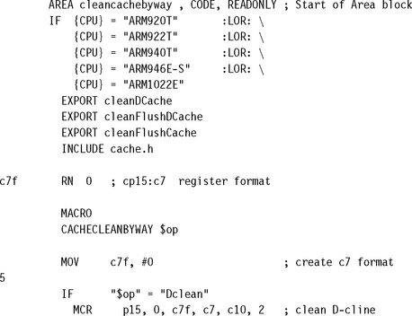
12.5.4 CLEANING THE D-CACHE USING WAY AND SET INDEX ADDRESSING
Some ARM cores support cleaning and flushing a single cache line using the way and set index to address its location in cache. The commands available to clean and flush a cache line byway are shown as MCR instructions in Table 12.5. Two commands flush a cache line, one flushes an instruction cache line, and another flushes a data cache line. The remaining two commands clean the D-cache: one cleans a cache line and another cleans and flushes a cache line.
Table 12.5
CP15:c7 Commands to clean cache using way and set index addressing.
| Command | MCR instruction | Core support |
| Flush instruction cache line | MCR p15, 0, Rd, c7, c5, 2 | ARM926EJ-S, ARM940T, ARM1026EJ-S |
| Flush data cache line | MCR p15, 0, Rd, c7, c6, 2 | ARM926EJ-S, ARM940T, ARM1026EJ-S |
| Clean data cache line | MCR p15, 0, Rd, c7, c10, 2 | ARM920T, ARM922T, ARM926EJ-S, ARM940T, ARM946E-S, ARM1022E, ARM1026EJ-S |
| Clean and flush data cache line | MCR p15, 0, Rd, c7, c14, 2 | ARM920T, ARM922T ARM926EJ-S, ARM940T, ARM946E-S, ARM1022E, ARM1026EJ-S |
Each core listed selects an individual cache line by its way and set index address. When using these instructions the value in core register Rd is the same for all four commands within a single processor core; however, the format of the bit fields within the register varies from processor to processor. The CP15:c7:Cm register format for cores that support cleaning and flushing a cache line by way is shown in Figure 12.11. To execute the command, create a value in a core register (Rd) in the desired CP15:c7 register format. The general form of the register includes two bit fields: one selects the way and the other selects the set in the way. Once the register is created, execute the desired MCR instruction to move the core register (Rd) to the CP15:c7 register.
The cleanDCache, cleanFlushDCache, and cleanFlushCache procedures for the ARM920T, ARM922T, ARM940T, ARM946E-S, and ARM1022E processors are shown in the following example.
EXAMPLE 12.3
We use a macro called CACHECLEANBYWAY to create the three procedures that clean, flush, or clean and flush the cache using way and set index addressing.
The macro uses constants in the header file cache.h to build a processor register in CP15:C7 register format (c7f) for the selected core. The first step is to set the c7f register to zero, which is used as the Rd input value in the MCR instruction to execute the selected operation. The macro then increments the c7f register according to the format in Figure 12.11, once for each written cache line. It increments the set index in the inner loop and the way index in the outer loop. Using these nested loops, it steps through and cleans all the cache lines in all the ways.
12.5.5 CLEANING THE D-CACHE USING THE TEST-CLEAN COMMAND
Two of the newer ARM cores, the ARM926EJ-S and ARM1026EJ-S, have commands to clean cache lines using a test-clean CP15:c7 register. The test clean command is a special clean instruction that can efficiently clean a cache when used in a software loop. The ARM926EJ-S and ARM1026EJ-S also support cleaning using set and way indexing; however, using the test clean command method of cleaning the D-cache is more efficient.
We use the commands shown in Table 12.6 in the following routines to clean the ARM926EJ-S and ARM1026EJ-S cores. The cleanDCache, cleanFlushDCache, and cleanFlushCache procedures for the ARM926EJ-S and ARM1026EJ-S processors are shown in Example 12.4.
Table 12.6
Commands to test clean a single D-cache line.
| Command | MCR instruction | Core Support |
| Test, clean D-cache line by loop | MCR p15, 0, r15, c7, c10, 3 | ARM926EJ-S, ARM1026EJ-S |
| Test, clean, and flush D-cache by loop | MCR p15, 0, r15, c7, c14, 3 | ARM926EJ-S, ARM1026EJ-S |
EXAMPLE 12.4
The test clean command finds the first dirty cache line and cleans it by transferring its contents to main memory. If another dirty cache exists in cache memory, then the Z flag will be zero.
To clean the cache, a software loop is created that uses the test clean command. By testing the Z flag and branching back to repeat the test, the processor loops through the test until the D-cache is clean. Note that the test clean command uses the program counter (r15) as the Rd register input to the MCR instruction.
12.5.6 CLEANING THE D-CACHE IN INTEL XSCALE SA-110 AND INTEL STRONGARM CORES
The Intel XScale and Intel StrongARM processors use a third method to clean their D-caches. The Intel XScale processors have a command to allocate a line in the D-cache without doing a line fill. When the processor executes the command, it sets the valid bit and fills the directory entry with the cache-tag provided in the Rd register. No data is transferred from main memory when the command executes. Thus, the data in the cache is not initialized until it is written to by the processor. The allocate command, shown in Table 12.7, has the beneficial feature of evicting a cache line if it is dirty.
Table 12.7
Intel XScale CP15:c7 commands to allocate a D-cache line.
| Command | MCR instruction | Core supported |
| Allocate line in data cache | MCR p15, 0, Rd, c7, c2, 5 | XScale |
The Intel StrongARM and Intel XScale processors require an additional technique to clean their caches. They need a dedicated area of unused cached main memory to clean the cache. By software design the memory block is dedicated to cleaning the cache only.
The Intel StrongARM and Intel XScale processors can be cleaned by reading this fixed block of memory because they use a round-robin replacement policy. If a routine is executed that forces the core to sequentially read an area of cached main data memory equal to the size of the cache, then the series of reads will evict all current cache lines and replace them with data blocks from the dedicated scratch read area. When the read sequence completes, the cache will contain no important data because the dedicated read block has no useful information in it. At this point, the cache can be flushed without fear of losing valued cached data.
We use this technique to clean the Intel StrongARM D-cache and the Intel XScale mini D-cache. The cleanDCache, cleanFlushDCache, and cleanFlushCache procedures for the Intel XScale and Intel StrongARM processors are shown in the following example. There is one additional procedure, called cleanMiniDCache, provided to clean the mini D-cache in the Intel XScale processor.
EXAMPLE 12.5
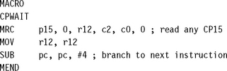
This example uses two macros, CPWAIT and CACHECLEANXSCALE. The CPWAIT macro is a three-instruction sequence used on Intel XScale processors to guarantee that CP15 operations execute without side effects. The macro executes these instructions so that enough processor cycles have completed to ensure that the CP15 command has completed and that the pipeline is clear of instructions. The CPWAIT macro is
The macro CACHECLEANXSCALE creates the procedures cleanDCache, cleanFlushDCache, and cleanFlushCache. The first part of the macro sets physical parameters for the routine. The first parameter, adr, is the starting virtual memory address of the dedicated area of memory used to clean the cache. The second parameter, nl is the total number of cache lines in the cache.
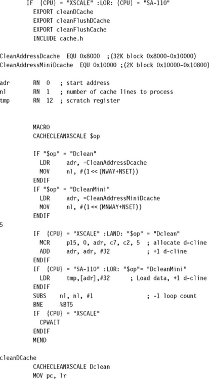
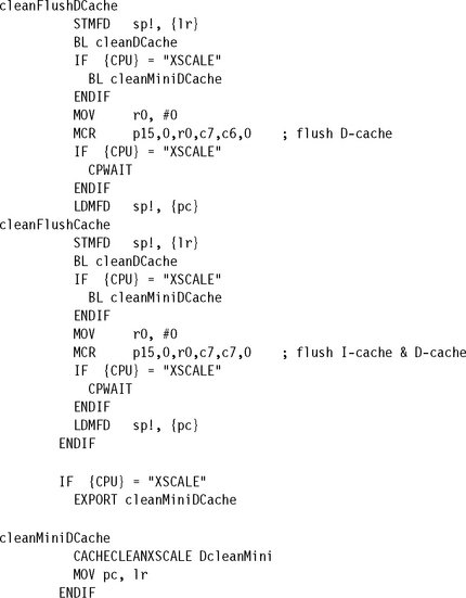
The macro then filters the needed commands to execute the clean operation for the two processor cores. The Intel XScale uses the allocate CP15:c7 command to clean the D-cache and reads a dedicated cached memory block to clean the mini D-cache. The Intel StrongARM reads from a dedicated area of memory to clean its D-cache.
Finally, we use the macro several times to create the cleanDCache, cleanFlushDCache, cleanFlushCache, and cleanMiniDCache procedures.
12.5.7 CLEANING AND FLUSHING PORTIONS OF A CACHE
ARM cores support cleaning and flushing a single cache line by reference to the location it represents in main memory. We show these commands as MCR instructions in Table 12.8.
Two of the commands flush a single cache line, one flushes the instruction cache, and the other flushes the data cache. There are also two commands to clean the data cache: one that cleans a single cache line and another that cleans and flushes a single cache line.
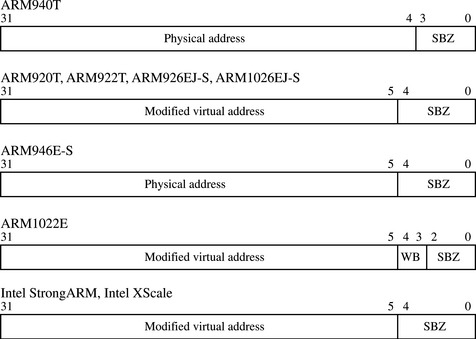
When using these instructions the value in core register Rd is the same for all four commands within the same processor, and its contents must be the value needed to set the CP15:c7 register. However, the format of the bit values in the CP15:c7 register vary slightly from processor to processor. Figure 12.12 shows the register format for cores that support cleaning and flushing a cache line by its modified virtual address if the core has an MMU, or its physical address if it has an MPU.
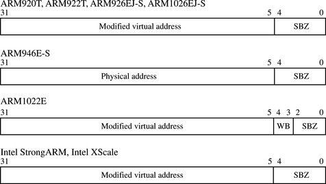
Figure 12.12 CP15:c7 Register Format when cleaning and flushing a cache line referenced by its origin in main memory.
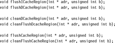
We use the four commands to create six routines, which clean and/or flush the cache lines in the cache that represent a region of memory:
![]() flushICacheRegion flushes the cache lines from the I-cache representing a region of main memory.
flushICacheRegion flushes the cache lines from the I-cache representing a region of main memory.
![]() flushDCacheRegion flushes the cache lines from the D-cache representing a region of main memory.
flushDCacheRegion flushes the cache lines from the D-cache representing a region of main memory.
![]() cleanDCacheRegion cleans the cache lines from the D-cache representing a region of main memory.
cleanDCacheRegion cleans the cache lines from the D-cache representing a region of main memory.
![]() cleanFlushDcacheRegion cleans and flushes the cache lines from the D-cache representing a region of main memory.
cleanFlushDcacheRegion cleans and flushes the cache lines from the D-cache representing a region of main memory.
![]() flushCacheRegion flushes the cache lines representing a region of main memory from both the I-cache and D-cache.
flushCacheRegion flushes the cache lines representing a region of main memory from both the I-cache and D-cache.
![]() cleanFlushCacheRegion cleans and flushes the D-cache and then flushes the I-cache.
cleanFlushCacheRegion cleans and flushes the D-cache and then flushes the I-cache.
All the procedures have two arguments passed to them, the starting address in main memory (adr) and the size of the region in bytes (b). The C function prototypes are
Care should be taken when using the clean cache region procedures. The use of these procedures is most successful on small memory regions. If the size of the region is several times larger than the cache itself, it is probably more efficient to clean the entire cache using one of the clean cache procedures provided in Sections 12.5.4, 12.5.5, and 12.5.6.
The region procedures are available on a limited set of ARM cores. Figure 12.12 lists the cores that support cleaning and flushing by address. They are also listed at the start of the code in the following example.
EXAMPLE 12.6
The macro takes the input address and truncates it to a cache line boundary. This truncation always addresses the first double word in the cache line of an ARM1022E (see Figure 12.12). The macro then takes the size argument and converts it from bytes to cache lines. The macro uses the number of cache lines as a counter variable to loop through the selected flush or clean operation, incrementing the address by a cache line size at the end of each loop. It exits when the counter reaches zero.
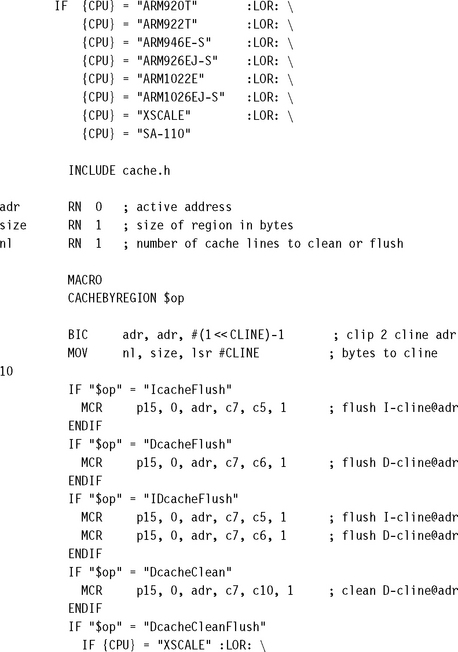
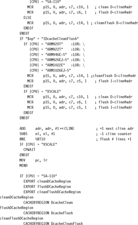
Finally, using the CACHEBYREGION macro, we either create three procedures if the core is an Intel StrongARM, which has a limited command set, or all six procedures for the remainder of the processors that have split caches.
12.6 CACHE LOCKDOWN
Cache lockdown is a feature that enables a program to load time-critical code and data into cache memory and mark it as exempt from eviction. Code or data in lockdown provides faster system response because it is held in the cache memory. Cache lockdown avoids the problem of unpredictable execution times that result from the cache line eviction process, a normal part of cache operation.
The purpose of locking information in cache is to avoid the cache miss penalty. However, because any cache memory used for lockdown is unavailable for caching other parts of main memory, the useful cache size is reduced.
The ARM core allocates fixed units of the cache for lockdown. The unit size that ARM cores allocate in lockdown is a way. For example, a four-way set associative cache allows locking code or data in units that are 1/4th of the cache size. The cached core always reserves at least one way for normal cache operation.
Some instructions that are candidates for locking in cache are the vector interrupt table, interrupt service routines, or code for a critical algorithm that the system uses extensively. On the data side, frequently used global variables are good candidates for lockdown.
Data or code locked in an ARM cache core is immune from replacement. However, when the cache is flushed, the information in lockdown is lost and the area remains unavailable as cache memory. The cache lockdown routine must be rerun to restore the lockdown information.
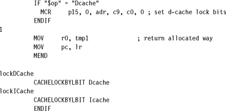
12.6.1 LOCKING CODE AND DATA IN CACHE
This section presents a procedure to lock code and data in cache. A typical sequence of C calls to lock code and data in cache is the following:
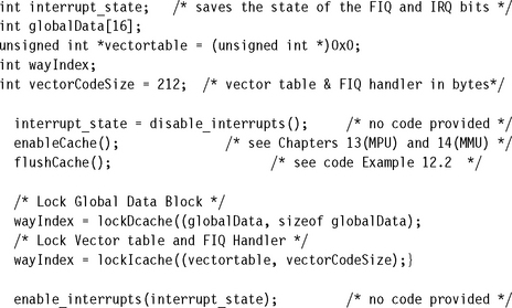
To begin, interrupts are disabled and the cache enabled. The procedure that disables interrupts is not shown. The flushCache procedure is one selected from the previous examples; the actual call used depends on the cache configuration and may also include cleaning the cache.
The function lockDCache locks a block of data in the D-cache; similarly, the function lockIcache locks a code block in the I-cache.
The lockdown software routines themselves must be located in noncached main memory. The code and data locked in cache must be located in cached main memory. It is important that the code and data locked in cache does not exist elsewhere in cache; in other words, if the contents of the cache are unknown, then flush the cache before loading. If the core is using a writeback D-cache, then clean the D-cache. Once the code and data are loaded in cache, reenable interrupts.
We present the code for the two functions lockDCache and lockIcache three different times because there are three different lockdown methods used to lock code in cache, depending on the architectural implementation. The first method locks code and data in the cache using way addressing techniques. The second uses a set of lock bits. In the third, code and data are locked in cache using a combination of a special allocate command and reading a dedicated block of main memory.
Table 12.9 lists the three examples that implement the two procedures lockDcache and lockIcache, the methods used, and the associated processors.
Table 12.9
| Example | Procedural method | Processor core |
| Example 12.7 | way addressing | ARM920T, ARM926EJ-S, ARM940T, ARM946E-S, ARM1022E, ARM1026EJ-S |
| Example 12.8 | lock bits | ARM926EJ-S, ARM1026EJ-S |
| Example 12.9 | special allocate command | XScale |
12.6.2 LOCKING A CACHE BY INCREMENTING THE WAY INDEX
The ARM920T, ARM926EJ-S, ARM940T, ARM946E-S, ARM1022E, and ARM1026EJ-S use way and set index addressing for lockdown. Two CP15:c9:c0 registers contain the victim counter reset registers described in Section 12.3.2. One of the registers controls the I-cache, and the other controls the D-cache. These registers are used to select the cache line within the way in which to lock the code or data.
The value written to the CP15:c7 register sets the victim reset value—the value that the victim counter is reset to when it increments beyond the number of ways in the core. The reset value is zero at power-up and is only changed by software if some portion of the cache is used for lockdown. When a portion of the cache is used for lockdown, the number of cache lines for caching information decreases by the number of cache lines locked down. Reading the register returns the current victim reset value. The MRC and MCR instructions to read and write to the two registers are shown in Table 12.10.
Table 12.10
Commands that lock data in cache by referencing its way.
| Command | MRC and MCR instructions | Processor core |
| Read D-cache lockdown base | MRC p15, 0, Rd, c9, c0, 0 | ARM920T, ARM926EJ-S, ARM940T, ARM946E-S, ARM1022E, ARM1026EJ-S |
| Write D-cache lockdown base | MCR p15, 0, Rd, c9, c0, 0 | ARM920T, ARM926EJ-S, ARM940T, ARM946E-S, ARM1022E, ARM1026EJ-S |
| Read I-cache lockdown base | MRC p15, 0, Rd, c9, c0, 1 | ARM920T, ARM926EJ-S, ARM940T, ARM946E-S, ARM1022E, ARM1026EJ-S |
| Write I-cache lockdown base | MCR p15, 0, Rd, c9, c0, 1 | ARM920T, ARM926EJ-S, ARM940T, ARM946E-S, ARM1022E, ARM1026EJ-S |
When reading or writing the lockdown base address, the format of the core register Rd used in the MCR and MRC instructions varies slightly from processor to processor. For each processor that uses these instructions, the format of the processor core Rd register is shown in Figure 12.13. To ensure that the command executes properly, be sure that the Rd register format matches that shown in the figure.
A special load command is also needed to lock instructions in cache. This special load command copies a cache-line-sized block of main memory to a cache line in the I-cache. The command and the format for the Rd register used in the instruction are shown in Table 12.11 and Figure 12.14.
Table 12.11
Command to lock a cache line in the I-cache.
| Command | MCR instruction | Processor core |
| Prefetch I-cache line by address | MCR p15, 0, Rd, c7, c13, 1 | ARM920T, ARM922T, ARM926EJ-S, ARM940T, ARM946E-S, ARM1022E, ARM1026EJ-S, StrongARM, XScale |
The following example shows lockDCache and lockICache routines for processors supporting lockdown using incremented way addressing. The return value for the two routines is the next available victim pointer base address.
EXAMPLE 12.7
The first part of the routine defines the registers used in the macro CACHELOCKBYWAY. The macro also uses constants in the header file cache.h shown in Figure 12.10.
The first line in the macro aligns the address (adr) to a cache line. The next three lines use the code size in bytes to determine the number of ways it takes to hold the code. Then the I-cache or D-cache current victim pointer is read from CP15:c9:c0.
The next few lines do some error checking to test for overfilling the cache and if the size of the code to load is zero.
To lock code or data in the cache of an ARM940T or ARM946E-S, there is a lock bit that must be set before locking a memory block in a cache line. The next instruction sets this bit and writes the data back to CP15:c9:c0.
At this point the code enters a nested loop, the outer loop selects the way, and the inner loop increments the cache lines within the way.
At the center of the two loops a prefetch instruction or load data command is used to lock a cache line in cache memory. To lock instructions, the macro writes to a special CP15:c7:c13 register that preloads the code segment from main memory. To lock data, a read of the data using an LDR instruction is all that is required.
The macro exits by clearing the lock bit in the CP15:c9:c0 register if it is an ARM940T or ARM946E-S. On all cores it sets the victim pointer to the next available way after the locked code or data.
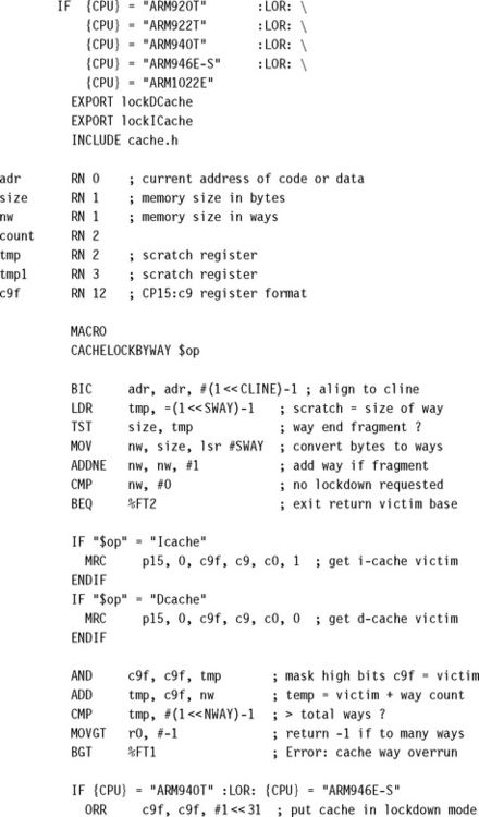
Finally, the macro is used twice to create the lockDCache and lockICache functions.
12.6.3 LOOKING A CACHE USING LOOK BITS
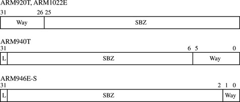
The ARM926EJ-S and ARM1026EJ-S lock code and data in cache using a set of lock bits, as shown in Figure 12.15. These two processors have a different Rd format for the CP15:c9 instructions, shown in Table 12.12. The four bits from zero to three represent each way in the four-way set associative cache in the two processors. If the bit’s set, the way is locked and contains either code if it is the I-cache or data if it is the D-cache. A locked way does not evict a cache line until it is unlocked. Clearing one of the L bits unlocks its way. This form of locking the cache allows the system code to individually select the way to lock or unlock.
Table 12.12
CP15:c9 Commands to lock cache using lockdown bits.
| Command | MRC and MCR instructions |
| Read I-cache lock page register | MRC p15, 0, c9f, c9, c0, 1 |
| Read D-cache lock page register | MRC p15, 0, c9f, c9, c0, 0 |
| Write I-cache lock page register | MCR p15, 0, c9f, c9, c0, 1 |
| Write I-cache lock page register | MCR p15, 0, c9f, c9, c0, 0 |
| Load code cache line at address | MCR p15, 0, Rd, c7, c13, 1 |
The ability to individually select a way to lock allows code to be more easily locked and unlocked in a system. The example code in this section implements a procedure that has the same programming interface used to lock data in the other cached cores.
The example lockDCache and lockICache procedures for the ARM926EJ-S and ARM1026EJ-S processors have the same input parameters. However, the code size is limited to a maximum of the way size, and it can be called up to three times. In the example, L bit 3 is always dedicated to cache. This is not a limitation of the processor hardware, but simply a limit placed on the procedure call to meet the needs of the programming interface.
The example procedure returns the L bit of the locked way if the size argument is one byte or greater. The procedure returns the next available L bit if the size is zero, and eight if there are no available ways for lockdown.
EXAMPLE 12.8
A macro called CACHELOCKBYLBIT generates both the lockDCache and lockICache functions. The macro also uses constants in the header file cache.h shown in Figure 12.10.
The macro starts by checking if the number of bytes to lock in cache is zero. Then it aligns the address adr to a cache line while determining the number of cache lines it takes to contain the code.
If the procedure is locking data in the D-cache, then it reads the lock register CP15:c9:c0:0. If the procedure is locking code in the I-cache, then it reads the lock register CP15:c9:c0:1. The resulting value is placed in the core c9f register. The L bits are also stored in the tmp register for later use.
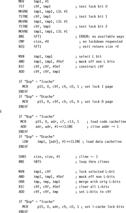
The next seven lines check the c9f register to see if there is a way available to store code or data; if not, the routine exits. If there is an available way, then the c9f format is modified in the next four lines to select the way in which to lock data. The c9f register is then used in the MCR instruction to select the way.
At this point the code enters a loop that fills the cache with locked code or data. If the procedure is locking code in the I-cache, it executes a prefetch I-cache line command. If locking data from external memory, it cleans, flushes, and loads a new cache line into the D-cache.
The macro exits by merging the saved L bits with the newly locked page and uses the result to create a new c9f register. The macro uses the c9f register in an MCR instruction to set the L bits in the CP15:c9:c0 cache lockdown register.
Finally, the CACHELOCKBYLBIT macro is used twice to create the lockDCache and lockICache functions.
12.6.4 LOCKING CACHE LINES IN THE INTEL XSCALE SA-110
The Intel XScale processor also has the capability to lock code and data into cache. This method requires the use of a set of CP15:c9 cache lockdown commands, shown in Table 12.13. The format of the CP15:c9:c2 register is shown in Figure 12.16. It also requires the CP15:c7 allocate D-cache line command we used to clean the D-cache in Example 12.5; this command is shown in Table 12.7.
Table 12.13
Fetch and Allocate commands to lock code or data in cache on an Intel XScale processor.
| Command | MRC and MCR instructions |
| Fetch and lock I-cache line VA | MCR p15, 0, Rd, c9, c1, 0 |
| Unlock instruction cache | MCR p15, 0, Rd, c9, c1, 1 |
| Read data cache lock register | MRC p15, 0, Rd, c9, c2, 0 |
| Write data cache lock register and set/clear lock mode | MCR p15, 0, Rd, c9, c2, 0 |
| Unlock D-cache | MCR p15, 0, Rd, c9, c2, 1 |
In the Intel XScale processor, each set in the cache has a dedicated round-robin pointer that is increased sequentially each time an additional cache line in the cache is locked. Up to 28 of the 32 cache lines within a set can be locked in cache. Attempting to lock more than 28 cache lines in a set results in the line being allocated but not locked in cache.
The Intel XScale processor supports two uses for locking data in the D-cache. The first use simply locks main memory locations into the D-cache. In the second use, the allocate cache line command is used to reconfigure a portion of the cache as data RAM; in that case, the portion of cache allocated is not initialized and needs a write from the processor core to contain valid data. In our example we initialize the memory to zero.
EXAMPLE 12.9
The first part of the routine defines the registers used in the macro CACHELOCKREGION. The macro also uses constants in the header file cache.h shown in Figure 12.10.
The macro starts by aligning the address (adr) to a cache line and determining the number of cache lines it takes to contain the code.
If the procedure is locking data in the D-cache, then the next few lines drain the write buffer and unlock the D-cache. Locking data in the D-cache requires an unlock command that must be issued prior to locking a D-cache line. The macro sets this bit by writing a one to the CP15:c9:c2:0 register.
At this point the code enters a loop that fills the cache with locked code or data. If the procedure is locking code in the I-cache, it executes a lock I-cache line command. If it is locking data from external memory, it cleans, flushes, and loads a new cache line into the D-cache. If creating data RAM, it allocates a D-cache line and drains the write buffer to protect against errors that might result from trying to lock more than 28 sets. It then initializes the cache line to zero using STRD instructions.
The macro exits by clearing the lock bit on cache load CP15 register if it is locking D-cache data.
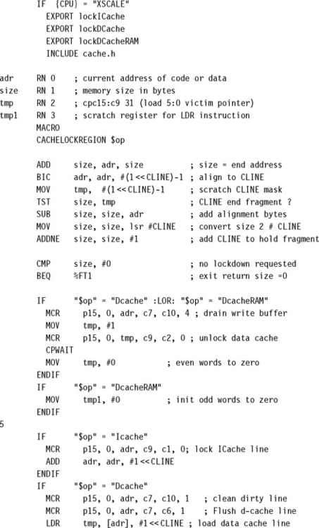
Finally, the macro is used three times to create the lockICache, lockDCache, and lockDCacheRAM functions.
12.7 CACHES AND SOFTWARE PERFORMANCE
Here are a few simple rules to help write code that takes advantage of cache architecture.
Most regions in a memory system are configured to have both the caches and write buffer enabled, taking maximum advantage of the cache architecture to reduce average memory access time. For more information on regions and the configuration of cache and write buffers operation within them, refer to Chapter 13 if you are using an ARM processor core with a memory protection unit and Chapter 14 if you are using an ARM processor core with a memory management unit.
Memory-mapped peripherals frequently fail if they are configured to use cache or the write buffer. It is best to configure them as noncached and nonbuffered memory, which forces the processor to read the peripheral device on every memory access, rather than use what would be stale data from cache.
Try to place frequently accessed data sequentially in memory, remembering that the cost of fetching a new data value from main memory requires a cache line fill. If the data in the cache line is used only once before it is evicted, performance will be poor. Placing data in the same cache line has the effect of actively forcing more cache hits by packing data close together to take advantage of spatial locality. It is most important to keep the data accessed by a common routine close together in main memory.
Try to organize data so reading, processing, and writing is done in cache-line-sized blocks whose lower main memory address matches the starting address of the cache line.
The best general approach is to keep code routines small and to group related data close together. The smaller the code, the more likely it is to be cache efficient.
Linked lists can reduce program performance when using a cache because searching the list results in a high number of cache misses. When accessing data from a linked list, a program fetches data in a more random fashion than it would if it were accessing the data from a sequential array. This hint really applies to searching any unordered list. The way you choose to search for data may require a performance analysis of your system.
However, it is important to remember that there are other factors that play a greater role in system performance than writing code to efficiently use cache. See Chapters 5 and 6 for efficient programming techniques.
12.8 SUMMARY
A cache is a small, fast array of memory placed between the processor and main memory. It is a holding buffer that stores portions of recently referenced system memory. The processor uses cache memory in preference to system memory whenever possible to increase average system performance.
A write buffer is a very small FIFO memory placed between the processor core and main memory, which helps free the processor core and cache memory from the slow write time associated with writing to main memory.
The principle of locality of reference states that computer software programs frequently run small loops of code that repeatedly operate on local sections of data memory and explains why the average system performance increases significantly when using a cached processor core.
There are many terms used by the ARM community to describe features of cache architecture. As a convenience we have created Table 12.14, which lists the features of all current ARM cached cores.
The cache line is a fundamental component in a cache and contains three parts: a directory store, a data section, and status information. The cache-tag is a directory entry indicating where a cache line was loaded from main memory. There are two common status bits within the cache: the valid bit and the dirty bit. The valid bit is set when the associated cache line contains active memory. The dirty bit is active when the cache is using a writeback policy and new data has been written to cache memory.
The placement of a cache before or after the MMU is either physical or logical. A logical cache is placed between the processor core and the MMU, and references code and data in a virtual address space. A physical cache is placed between the MMU and main memory, and references code and data memory using physical addresses.
A direct-mapped cache is a very simple cache architecture where there is a single location in cache for a given main memory location. A direct-mapped cache is subject to thrashing. To reduce thrashing, a cache is divided into smaller equal units called ways. The use of ways provides multiple storage locations in cache for a single main memory address. These caches are known as set associative caches.
The core bus architecture helps determine the design of a cached system. A Von Neumann architecture uses a unified cache to store code and data. A Harvard architecture uses a split cache: it has one cache for instructions and a separate cache for data.
The cache replacement policy determines which cache line is selected for replacement on a cache miss. The configured policy defines the algorithm a cache controller uses to select a cache line from the available set in cache memory. The cache line selected for replacement is a victim. The two replacement policies available in ARM cached cores are pseudorandom and round-robin.
There are two policies available when writing data to cache memory. If the controller only updates cache memory, it is a writeback policy. If the cache controller writes to both the cache and main memory, it is a writethrough policy.
There are two policies a cache controller uses to allocate a cache line on a cache miss. A read-allocate policy allocates a cache line when data is read from main memory. A write-allocate policy allocates a cache line on a write to main memory.
ARM uses the term clean to mean forcing a copyback of data in the D-cache to main memory. ARM uses the term flush to mean invalidating the contents of a cache.
Cache lockdown is a feature provided by some ARM cores. The lockdown feature allows code and data to be loaded into cache and marked as exempt from eviction.
We also provided example code showing how to clean and flush ARM cached cores, and to lock code and data in cache.