
Multirate Signal Processing for Software Radio Architectures
Fred Harris, Elettra Venosa and Xiaofei Chen, San Diego State University, Department of Electrical and Computer Engineering, San Diego, CA, USA, [email protected], [email protected], [email protected]
Abstract
This chapter is about multirate signal processing and the potential that it brings to modern (software) radios. Optimizing the sample rate while processing signals provides many advantages to digital systems. Costs and computational complexity reduction, improved performance and reduced chip size are just some of them. Digital filters, up converters, and down converters are the basic elements for designing multirate architectures and their introduction in this chapter is necessary for a deeper understanding of perfect reconstruction polyphase channelizers, which are the key modules of the modern digital radios. This chapter follows a very practical approach. We decided to keep the mathematical formulation to a minimum to allow more space for concepts and figures. References are given at the end of the chapter for the interested readers.
Keywords
Software defined radio; Polyphase filter bank; Polyphase channelizer; Digital up converter; Digital down converter; Digital filter; Nyquist pulse; Perfect reconstruction property; MMDM; Multirate signal processing; Resampling
After the introductory sections on resampling theory and basics of digital filters, the architectures of up and down converter channelizers are presented. Those paragraphs are followed by the main core of this chapter in which the authors present novel digital up converter (DUC) and digital down converter (DDC) architectures for software defined radios (SDRs) which are based on variations of standard polyphase channelizers.
The proposed DUC is able to simultaneously up convert multiple signals, having arbitrary bandwidths, to arbitrarily located center frequencies. On the other side of the communication chain, the proposed DDC is able to simultaneously down convert multiple received signals with arbitrary bandwidth and arbitrarily located in the frequency domain. Both the proposed structures avoid the digital data section replication, which is necessary in the current digital transmitters and receivers, when multiple signals have to be handled. Due to the inverse discrete Fourier transform (IDFT), performed by using inverse fast Fourier transform (IFFT) algorithm, embedded in the channelizers, the proposed architectures are very efficient in terms of total workload.
This chapter is structured into two main parts which are composed, in total, of 10 sections. Its structure is described in Figure 7.1. The first part provides preliminary concepts on the sampling process, resampling process of a digital signal, digital filters, multirate structures, standard M-path polyphase up and down converter channelizers as well as their modified versions that represent the core of the structures we present in the second part of this document. These are well known topics in the digital signal processing (DSP) area and they represent the necessary background for people who want to start learning about software radios. The second part of this chapter goes through new frontiers of the research presenting the novel transmitting and receiving designs for software radios and demonstrating, while explaining the way in which they work, the reasons that make them the perfect candidates for the upcoming cognitive radios.

1.07.1 Introduction
Signal processing is the art of representing, manipulating, and transforming wave shapes and the information content that they carry by means of hardware and/or software devices. Until 1960s almost entirely continuous time, analog technology was used for performing signal processing. The evolution of digital systems along with the development of important algorithms such as the well known fast Fourier transform (FFT), by Cooley and Tukey in 1965, caused a major shift to digital technologies giving rise to new digital signal processing architectures and techniques. The key difference between analog processing techniques and digital processing techniques is that while the first one processes analog signals, which are continuous functions of time; the second one processes sequences of values. The sequences of values, called digital signals, are series of quantized samples (discrete time signal values) of analog signals.
The link between the analog signals and their sampled versions is provided by the sampling process. When sampling is properly applied it is possible to reconstruct the continuous time signal from its samples preserving its information content. Thus the selection of the sampling rate is crucial: an insufficient sampling frequency causes, surely, irrecoverable loss of information, while a more than necessary sampling rate causes useless overload on the digital systems.
The string of words multirate digital signal processing indicates the operation of changing the sample rate of digital signals, one or multiple times, while processing them. The sampling rate changes can occur at a single or multiple locations in the processing architecture. When the multirate processing applied to the digital signal is a filtering then the digital filter is named multirate filter; a multirate filter is a digital filter that operates with one or more sample rate changes embedded in the signal processing architecture. The opportunity of selecting the most appropriate signal sampling rate at different stages of the processing architecture, rather than having a single (higher) sampling rate, enhances the performance of the system while reducing its implementation costs. However, the analysis and design of multirate systems could result complicated because of the fact that they are time-varying systems. It is interesting to know that the first multirate filters and systems were developed in the context of control systems. The pioneer papers on this topic were published in the second half of 1950s [1–3]. Soon the idea spilled in the areas of speech, audio, image processing [4,5], and communication systems [6]. Today, multirate structures seem to be the optimum candidates for cognitive and software defined radio [7–11] which represents the frontier of innovation for the upcoming communication systems.
One of the well known techniques that find its most efficient application when embedded in multirate structures is the polyphase decomposition of a prototype filter. The polyphase networks, of generic order M, originated in the late 1970s from the works by Bellanger et al. [12,13]. The term polyphase is the aggregation of two words: poly, that derives from the ancient greek word polys, which means many, and phase. When applied to an M-path partitioned filter these two words underline the fact that, on each path, each aliased filter spectral component, experiences a unique phase rotation due to both their center frequencies and the time delays, which are different in each path because of the way in which the filter has been partitioned. When all the paths are summed together the undesired spectral components, having phases with opposite polarity, cancel each other while only the desired components, which experience the same phase on all the arms of the partitions, constructively add up. By applying appropriate phase rotators to each path we can arbitrarily change the phases of the spectral components selecting the spectral component that survives as a consequence of the summation. It is interesting to know that the first applications of the polyphase networks were in the areas of real-time implementation of decimation and interpolation filters, fractional sampling rate changing devices, uniform DFT filter banks as well as perfect reconstruction analysis/synthesis systems. Today polyphase filter banks, embedded in multirate structures, are used in many modern DSP applications as well as in communication systems where they represent, according to the author’s belief, one of the most efficient options for designing software-based radio.
The processing architecture that represents the starting point for the derivation of the standard polyphase down converter channelizer is the single channel digital down converter. In a digital radio receiver this engine performs the operations of filtering, frequency translation and resampling on the intermediate frequency (IF) signals. The resampling is a down sampling operation for making the signal sampling rate commensurate to its new reduced bandwidth. When the output sampling rate is selected to be an integer multiple of the signal’s center frequency, the signal spectrum is shifted, by aliasing, to base-band and the complex heterodyne defaults to unity value disappearing from the processing path. The two remaining operations of filtering and down sampling are usually performed in a single processing architecture (multirate filter). After exchanging the positions of the filter and resampler, by applying polyphase decomposition, we achieve the standard M-path polyphase down converter channelizer which shifts a single narrowband channel to base-band while reducing its sampling rate. By following a similar procedure the standard up converter channelizer can also be obtained. It performs the operation of up converting while interpolating a single narrowband channel.
When the polyphase channelizer is used in this fashion the complex phase rotators can be applied to each arm to select, by coherent summation, a desired channel arbitrarily located in the frequency domain. Moreover, the most interesting and efficient application of this engine is in the multichannel scenario. When the inverse discrete Fourier transform block is embedded, the polyphase channelizer acquires the capability to simultaneously up and down convert, by aliasing, multiple, equally spaced, narrowband channels having equal bandwidths. Due to its computational efficiency, the polyphase channelizer, and its modified versions, represents the best candidate for building up new flexible multichannel digital radio architectures [14] like software defined radio promises to be.
Software defined radio represents one of the most important emerging technologies for the future of wireless communication services. By moving radio functionality into software, it promises to give flexible radio systems that are multi-service, multi-standard, multi-band, reconfigurable, and reprogrammable by software. The goal of software defined radio is to solve the issue of optimizing the use of the radio spectrum that is becoming more and more pressing because of the growing deployment of new wireless devices and applications [15–18].
In the second part of this chapter we address the issue of designing software radio architectures for both the transmitter and the receiver. The novel structures are based on modified versions of the standard polyphase channelizer, which provides the system with the capability to optimally adapt its operating parameters according to the surrounding radio environment [7,19–21]. This implies, on the transmitter side, the capability of the radio to detect the available spectral holes [22,23] in the spanned frequency range and to dynamically use them for sending signals having different bandwidths at randomly located center frequencies. The signals could be originated from different information sources or they could be spectral partitions of one signal, fragmented because of the unavailability of free space in the radio spectrum or for protecting it from unknown and undesired detections.
The core of the proposed transmitter is a synthesis channelizer [24]. It is a variant of the standard M-path polyphase up converter channelizer [6,8] that is able to perform 2-to-M up sampling while shifting, by aliasing, all the base-band channels to the desired center frequencies. Input signals with bandwidths wider than the synthesis channelizer bandwidth are pre-processed through small down converter channelizers that disassemble their bandwidths into reduced bandwidth sub-channels. The proposed transmitter avoids the need to replicate the sampled data section when multiple signals have to be simultaneously transmitted and it also allows partitioning of the signal spectra, when necessary, before transmitting them. Those spectral fragments will be reassembled in the receiver after being shifted to base-band without any loss of energy because perfect reconstruction filters are used as low-pass prototype in the channelizer polyphase decompositions.
On the other side of the communication chain, a cognitive receiver has to be able to simultaneously detect multiple signals, recognize, when necessary, all their spectral partitions, filter, down convert and recompose them without energy losses [7] independently of their bandwidths or center frequencies. An analysis channelizer is the key element of the proposed receiver [7]. This engine is able to perform M-to-2 down sampling while simultaneously demodulating, by aliasing, all the received signal spectra having arbitrary bandwidths residing at arbitrary center frequencies [9]. Post-processing up converter channelizers are used for reassembling, from the analysis channelizer base-line channels, signal bandwidths wider than the analysis channelizer channel bandwidth.
In the transmitter complex frequency rotators apply the appropriate frequency offsets for arbitrary center frequency positioning of the spectra. When the frequency rotators are placed in the proposed receiver, they are responsible for perfect DC alignment of the down converted signals.
This chapter is composed of 10 main sections. The first four sections are dedicated to the basics of digital signal processing, multirate signal processing, and polyphase channelizers. These sections contain preliminary concepts necessary for completely understanding the last sections of this work in which actual research issues on software radio (SR) architecture design are discussed and innovative results are presented. In particular, Section 1.07.2 recalls basic concepts on the resampling process of a discrete time signal as opposed to the sampling process of an analog, continuous time, signal. Section 1.07.3 introduces the readers to digital filters providing preliminaries on their design techniques. Section 1.07.5 presents the standard single path architectures for down sampling and up sampling digital signals. Section 1.07.6 introduces the standard version of the M-path polyphase down and up converter channelizers. Both of them are derived, step by step, by the single path structures that represent the current state of the technology. In Section 1.07.7 we present the modified versions of these engines. These are the structures that give form to the proposed digital down and up converters for SDRs which are presented in Section 1.07.9 which also provides the simulation results. Section 1.07.8 introduces the readers to the concept of software radio while Section 1.07.10 gives concluding remarks along with suggestions for future research works in this same area.
1.07.2 The Sampling process and the “Resampling” process
In the previous section we mentioned that the sampling process is the link between the continuous time world and the discrete time world. By sampling a continuous time signal we achieve its discrete time representation. When sampling frequency is properly selected the sampling process becomes invertible and it is possible to re-shift from the discrete time representation to the continuous time representation of a signal maintaining its information content during the process.
It is well known that, when the signal is bandlimited and has no frequency components above ![]() it can be uniquely described by its samples taken uniformly at frequency
it can be uniquely described by its samples taken uniformly at frequency
![]() (7.1)
(7.1)
Equation (7.1) is known as Nyquist sampling criterion (or uniform sampling theorem) and the sampling frequency ![]() is called the Nyquist sampling rate. This theorem represents a theoretically sufficient condition for reconstructing the analog signal from its uniformly spaced samples.
is called the Nyquist sampling rate. This theorem represents a theoretically sufficient condition for reconstructing the analog signal from its uniformly spaced samples.
Even though sampling is practically implemented in a different way, it is convenient, in order to facilitate the learning process, to represent it as a product of the analog waveform, ![]() , with a periodic train of unit impulse functions defined as
, with a periodic train of unit impulse functions defined as
![]()
where ![]() is the sampling period. By using the shifting property of the impulse function we obtain
is the sampling period. By using the shifting property of the impulse function we obtain
![]() (7.2)
(7.2)
A pictorial description of Eq. (7.2) is given in Figure 7.2.

Figure 7.2 Sampling process as a product of the analog waveform, ![]() , with a periodic train of unit impulse functions
, with a periodic train of unit impulse functions ![]() .
.
For facilitating the readers’ understanding of the uniform sampling effects on the bandlimited continuous time signal, ![]() , we shift from time domain to the frequency domain where we are allowed to use the properties of the Fourier transform. The product of two functions in time domain becomes the convolution of their Fourier transforms in the frequency domain. Thus, if
, we shift from time domain to the frequency domain where we are allowed to use the properties of the Fourier transform. The product of two functions in time domain becomes the convolution of their Fourier transforms in the frequency domain. Thus, if ![]() is the Fourier transform of
is the Fourier transform of ![]() and
and ![]() is the Fourier transform of
is the Fourier transform of ![]() , then the Fourier transform of
, then the Fourier transform of ![]() is
is
![]()
where ![]() indicates linear convolution and
indicates linear convolution and
![]()
Note that the Fourier transform of a impulse train is another impulse train with the values of the periods reciprocally related to each other. Then in the frequency domain Eq. (7.2) becomes
![]() (7.3)
(7.3)
whose pictorial view is shown in Figure 7.3.
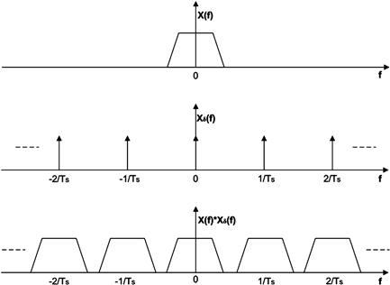
From Eq. (7.3) we conclude that the spectrum of the sampled signal, in the original signal bandwidth ![]() , is the same as the continuous time one (except for a scale factor,
, is the same as the continuous time one (except for a scale factor, ![]() ) however, as a consequence of the sampling process, this spectrum periodically repeats itself with a period of
) however, as a consequence of the sampling process, this spectrum periodically repeats itself with a period of ![]() . We can easily recognize that it should be possible to recover the original spectrum (associated to the spectral replica which resides in
. We can easily recognize that it should be possible to recover the original spectrum (associated to the spectral replica which resides in ![]() , by filtering the periodically sampled signal spectrum with an appropriate low-pass filter.
, by filtering the periodically sampled signal spectrum with an appropriate low-pass filter.
Notice, from Eq. (7.3) that the spacing, ![]() , between the signal replicas is the reciprocal of the sampling period
, between the signal replicas is the reciprocal of the sampling period ![]() . A small sampling period corresponds to a large space between the spectral replicas.
. A small sampling period corresponds to a large space between the spectral replicas.
A fundamental observation, regarding the selection of the uniform sampling frequency, needs to be done at this point: when the sampling rate is selected to be less than the maximum frequency component of the bandlimited signal ![]() the periodic spectral replicas overlap each other. The amount of the overlap depends of the selected sampling frequency. Smaller the sampling frequency, larger the amount of overlap experienced by the replicas. This phenomenon is well known as aliasing. When aliasing occurs it is impossible to recover the analog signal from its samples. When
the periodic spectral replicas overlap each other. The amount of the overlap depends of the selected sampling frequency. Smaller the sampling frequency, larger the amount of overlap experienced by the replicas. This phenomenon is well known as aliasing. When aliasing occurs it is impossible to recover the analog signal from its samples. When ![]() the spectral replicas touch each other without overlapping and it is theoretically (but not practically) possible to recover the analog signal from its samples; however a filter with infinite number of taps would be required. As a matter of practical consideration, we need to specify here that the signals (and filters) of interest are never perfectly bandlimited and some amount of aliasing always occurs as effect of sampling however some techniques can be used to limit the phenomena making it less harmful.
the spectral replicas touch each other without overlapping and it is theoretically (but not practically) possible to recover the analog signal from its samples; however a filter with infinite number of taps would be required. As a matter of practical consideration, we need to specify here that the signals (and filters) of interest are never perfectly bandlimited and some amount of aliasing always occurs as effect of sampling however some techniques can be used to limit the phenomena making it less harmful.
After the sampling has been applied the amplitude of each sample is one from an infinite set of possible values. This is the reason for which the samples are not compatible with a digital system yet. A digital system can, in fact, only deal with a finite number of values. The digital samples need to be quantized before being sent to the digital data system. The quantization process limits the amplitude of the samples to a finite set of values. After the quantization process the signal can still be recovered, however some additional imprecision is added to it. The amount of imprecision depends of the quantization levels used in the process and it has the same effect on the signal as white noise. This is the reason for which it is referred to as quantization noise. The sampling of a continuous time signal and the quantization of its discrete time samples are both performed with devices called analog-to-digital converters (ADCs).
The selection of the appropriate sampling rate is a fundamental issue faced when designing digital communication systems. In order to preserve the signal, the Nyquist criterion must be always satisfied. Also, it is not difficult to find tasks for which, at some points in the digital data section of the transmitter and the receiver, it is recommended to have more than two samples per signal bandwidth. On the other hand, large sample rates cause an increase in the total workload of the system. Thus the appropriate sampling rate must be selected according to both the necessities: to have the required number of samples and to minimize the total workload. Most likely the optimum sampling frequency changes at different points in the digital architecture. It would be a huge advantage to have the option of changing the signal sampling rate at different parts in the systems while processing it, thus optimizing the number of samples as a function of the requirements. The process of changing the sampling rate of a digital signal is referred to as resampling process. The resampling process is the key concept in multirate signal processing.
After the brief previous discussion about the sampling process of a continuous time signal, we address now the process of resampling an already sampled signal. Notice that when a continuous time signal is sampled there are no restrictions on the sample rate or the phase of the sample clock relative to the time base of the continuous time signal. On the other hand, when we resample an already sampled signal, the output sample locations are intimately related to the input sample positions. A resampled time series contains samples of the original input time series separated by a set of zero valued samples. The zero valued time samples can be the result of setting a subset of input sample values to zero or the result of inserting zeros between existing input sample values. Both options are shown in Figure 7.4. In the first example shown in this figure, the input sequence is resampled 2-to-l, keeping every second input sample starting at sample index 0 while zeroing the interim samples. In the second example, the input sequence is resampled 1-to-2, keeping every input sample but inserting a zero valued sample between each input samples. These two processes are called down sampling and up sampling respectively.
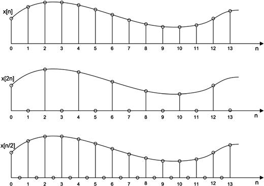
The non-zero valued samples of two sequences having the same sample rate can occur at different time indices (i.e., the same sequence can have different initial time offset) as in Figure 7.5 in which the two 2-to-1 down sampled sequences, ![]() and
and ![]() , have different starting time index, 0 and 1, which gives equal magnitude spectral components with different phase profiles. This is explicitly shown in Figures 7.6 and 7.7, in which the time domain and the frequency domain views of the resampled sequences
, have different starting time index, 0 and 1, which gives equal magnitude spectral components with different phase profiles. This is explicitly shown in Figures 7.6 and 7.7, in which the time domain and the frequency domain views of the resampled sequences ![]() and
and ![]() are depicted respectively. Remember, in fact, the time shifting property of the discrete Fourier transform (DFT) for which a shift in time domain is equivalent to a linear phase shift in the frequency domain. The different phase profiles play a central role in multirate signal processing.
are depicted respectively. Remember, in fact, the time shifting property of the discrete Fourier transform (DFT) for which a shift in time domain is equivalent to a linear phase shift in the frequency domain. The different phase profiles play a central role in multirate signal processing.


The M zero valued samples inserted between the signal samples create M periodic replicas of the original spectrum at the frequency locations k/M, with ![]() in the normalized domain. This observation suggests that resampling can be used to affect translation of spectral bands, up and down conversion, without the use of sample data heterodynes.
in the normalized domain. This observation suggests that resampling can be used to affect translation of spectral bands, up and down conversion, without the use of sample data heterodynes.
In the following paragraphs we clarify this concept showing how to embed the spectral translation of narrowband signals in resampling filters and describe the process as aliasing.
A final comment about the resampling process is that it can be applied to a time series or to the impulse response of a filter, which, of course, is simply another time series. When the resampling process is applied to a filter, the architecture of the filter changes considerably and the filter is called multirate filter.
1.07.3 Digital filters
Filtering is the practice of processing signals which results in some changes of their spectral contents. Usually the change implies a reduction or filtering out some undesired input spectral components. A filter allows certain frequencies to pass while attenuating others. While analog filters operate on continuous-time signals, digital filters operate on sequences of discrete sampled value (see Figure 7.8) although digital filters perform many of the same functions as analog filters, they are different!
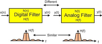
The two classes of filters share many of the same or analogous properties. In the standard order of our educational process we first learn about analog filters and later learn about digital filters. To ease the entry into the digital domain we emphasize the similarities of the two classes of filters. This order is due to fact that an analog filter is less abstract than a digital filter. We can touch the components of an analog filter; capacitors, inductors, resistors, operational amplifiers and wires. On the other hand a digital filter doesn’t have the same physical form because a digital filter is merely a set of instructions that perform arithmetic operations on an array of numbers. The operations can be weighted sums or inner products (see Figure 7.9). It is convenient to visualize the array as a list of uniformly spaced sample values of an analog waveform. The instructions to perform these operations can reside as software in a computer or microprocessor or as firmware in a dedicated collection of interconnected hardware elements.
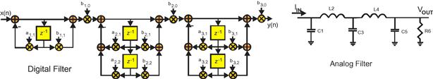
Figure 7.9 Digital filter: registers, adders, and multipliers. Analog filter, capacitor, inductors, and resistors.
Let us examine the similarities that are emphasized when we learn about digital filters with some level of prior familiarity with analog filters and the tools to describe them. Many analog filters are formed by interconnections of lumped linear components modeled as ideal capacitors, inductors, and resistors while others are formed by interconnections of resistors, capacitors, and operational amplifiers. Sampled data filters are formed by interconnections of registers, adders, and multipliers. Most analog filters are designed to satisfy relationships defined by linear time invariant differential equations. The differential equations are recursive which means the initial condition time domain response, called the homogeneous or undriven response, is a weighted sum of exponentially decaying sinusoids. Most sampled data filters are designed to satisfy relationships defined by linear time invariant difference equations. Here we find the first major distinction between the analog and digital filters: the difference equations for the sampled data filters can be recursive or non recursive. When the difference equations are selected to be recursive the initial condition response is, as it was for the analog filter, samples of a weighted sum of exponentially decaying sinusoids. On the other hand, when the difference equation is non recursive the initial condition response is anything the designer wants it to be and is limited only by her imagination but is usually designed to satisfy some frequency domain specifications.
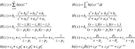
When we compare the two filter classes, analog and digital, we call attention to the similarities of the tools we use to describe, analyze, and design them. They are described by differential and difference equations which are weighted sums of signal derivates or weighted sums of delayed sequences. They both have linear operators or transforms, the Laplace transform ![]() , and the z transform
, and the z transform ![]() , that offer us insight into the internal structure of the differential or difference equations (see Figure 7.10). They both have operator descriptions that perform the equivalent functions. These are the integral operator, denoted by
, that offer us insight into the internal structure of the differential or difference equations (see Figure 7.10). They both have operator descriptions that perform the equivalent functions. These are the integral operator, denoted by ![]() , and the delay operator, denoted by
, and the delay operator, denoted by ![]() , in which reside the system memories or state of the analog and digital filters respectively. Both systems have transfer functions H(s) and H(z), ratios of polynomials in the operator variable s and z. The roots of the denominator polynomial, the operator version of the characteristic equation, are the filter poles. These poles describe the filter modes, the exponentially damped sinusoids, of the recursive structure. The roots of numerator polynomial are the filter zeros. The zeros describe how the filter internal mode responses are connected to the filter input and output ports. They tell us the amplitude of each response component, (called residues to impress us) in the output signal’s initial condition response. The transforms of the two filter classes have companion transforms the Fourier transform
, in which reside the system memories or state of the analog and digital filters respectively. Both systems have transfer functions H(s) and H(z), ratios of polynomials in the operator variable s and z. The roots of the denominator polynomial, the operator version of the characteristic equation, are the filter poles. These poles describe the filter modes, the exponentially damped sinusoids, of the recursive structure. The roots of numerator polynomial are the filter zeros. The zeros describe how the filter internal mode responses are connected to the filter input and output ports. They tell us the amplitude of each response component, (called residues to impress us) in the output signal’s initial condition response. The transforms of the two filter classes have companion transforms the Fourier transform ![]() and the sampled data Fourier series
and the sampled data Fourier series ![]() which describe, when they exist, the frequency domain behavior, sinusoidal steady state gain and phase, of the filters. It is remarkable how many similarities there are in the structure, the tools, and the time and frequency responses of the two types of filters. It is no wonder we emphasize their similarities.
which describe, when they exist, the frequency domain behavior, sinusoidal steady state gain and phase, of the filters. It is remarkable how many similarities there are in the structure, the tools, and the time and frequency responses of the two types of filters. It is no wonder we emphasize their similarities.
We spend a great deal of effort examining recursive digital filters because of the close relationships with their analog counterparts. There are digital filters that are mappings of the traditional analog filters. These include maximally flat Butterworth filters, equal ripple pass-band Tchebychev-I filters, equal ripple stop-band Tchebychev-II filters, and both equal ripple pass-band and equal ripple stop-band Elliptic filters. The spectra of these infinite impulse response (IIR) filters are shown in Figure 7.11. All DSP filter design programs offer the DSP equivalents of their analog recursive filter counterparts.

In retrospect, emphasizing similarities between the analog filter and the equivalent digital was a poor decision. We make this claim for a number of reasons. The first is there are limited counterparts in the analog domain to the non-recursive filter of the digital domain. This is because the primary element of the non recursive filter is the pure delay, represented by the delay operator ![]() . We cannot form a pure delay response, represented by the analog delay operator
. We cannot form a pure delay response, represented by the analog delay operator ![]() , in the analog domain as the solution of a linear differential equation. To obtain pure delay, we require a partial differential equation which offers the wave equation whose solution is a propagating wave which we use to convert distance to time delay. The propagation velocity of electromagnetic waves is too high to be of practical use in most analog filter designs but the velocity of sound waves in crystal structures enables an important class of analog filters known as acoustic surface wave (SAW) devices. Your cell phone contains one or more such filters. In general, most of us have limited familiarity with non-recursive analog filters so our first introduction to the properties and design techniques for finite duration impulse response (FIR) filters occurs in our DSP classes.
, in the analog domain as the solution of a linear differential equation. To obtain pure delay, we require a partial differential equation which offers the wave equation whose solution is a propagating wave which we use to convert distance to time delay. The propagation velocity of electromagnetic waves is too high to be of practical use in most analog filter designs but the velocity of sound waves in crystal structures enables an important class of analog filters known as acoustic surface wave (SAW) devices. Your cell phone contains one or more such filters. In general, most of us have limited familiarity with non-recursive analog filters so our first introduction to the properties and design techniques for finite duration impulse response (FIR) filters occurs in our DSP classes.
The second reason for not emphasizing the similarities between analog and digital filters is that we start believing the statement that “a digital filter is the same as an analog filter” and that all the properties of one are embedded in the other. That seemed like an ok perspective the first 10 or 20 times we heard that claim. The problem is, it is not true! The digital filter has a resource the analog filter does not have! The digital filter can perform tasks the analog filter cannot do! What is that resource? It is the sampling clock! We can do applied magic in the sampled data domain by manipulating the sample clock. There is no equivalent magic available in the analog filter domain! Analog designers shake their heads in disbelief when they see what a multirate filter can do. Actually digital designers also shake their heads in disbelief when they learn that manipulating the clock can accomplish such amazing things.
We might ask how can the sampling clock affect the performance or more so, enhance the capabilities of a digital filter? Great question! The answer my friend is written in the way define frequency of a sampled data signal. Let us review how frequency as we understand it in the analog world is converted to frequency in the digital world. We now present a concise review of complex and real sinusoids with careful attention paid to their arguments.
The exponential function ![]() has the interesting property that it satisfies the differential equation shown in Eq. (7.4). This means the exponential function replicates under the differential operator, an important property inherited by real and complex sinusoids. It is easy to verify that the Taylor series shown in Eq. (7.5) satisfies Eq. (7.4). When we replace the argument “x” of Eq. (7.5) with the argument “
has the interesting property that it satisfies the differential equation shown in Eq. (7.4). This means the exponential function replicates under the differential operator, an important property inherited by real and complex sinusoids. It is easy to verify that the Taylor series shown in Eq. (7.5) satisfies Eq. (7.4). When we replace the argument “x” of Eq. (7.5) with the argument “![]() ” we obtain the series shown in Eq. (7.6) and when we gather the terms corresponding to the even and odd powers respectively of the argument “
” we obtain the series shown in Eq. (7.6) and when we gather the terms corresponding to the even and odd powers respectively of the argument “![]() ” we obtain the partitioned series shown in Eq. (7.7). We recognize that the two Taylor series of the partitioned Eq. (7.7) are the Taylor series of the cosine and sine which we show explicitly in Eq. (7.8). We note that the argument of both the real exponential and of the complex exponential must be dimensionless otherwise we would not be able to sum the successive powers of the series. We also note that the units of the argument “
” we obtain the partitioned series shown in Eq. (7.7). We recognize that the two Taylor series of the partitioned Eq. (7.7) are the Taylor series of the cosine and sine which we show explicitly in Eq. (7.8). We note that the argument of both the real exponential and of the complex exponential must be dimensionless otherwise we would not be able to sum the successive powers of the series. We also note that the units of the argument “![]() ” are radians, a dimensionless unit formed by the ratio of arc length on a circle normalized by the radius of the circle. When we replace the “
” are radians, a dimensionless unit formed by the ratio of arc length on a circle normalized by the radius of the circle. When we replace the “![]() ” argument of Eq. (7.8) with a time varying angle “
” argument of Eq. (7.8) with a time varying angle “![]() ” we obtain the time function shown in Eq. (7.9). The simplest time varying angle is one the changes linearly with time,
” we obtain the time function shown in Eq. (7.9). The simplest time varying angle is one the changes linearly with time, ![]() , which when substituted in Eq. (7.9) we have Eq. (7.10). All of this discussion leads us to the next statement. Since the argument of a sinusoid has the dimensionless units radians and the units of “t” has units of seconds, then the units of
, which when substituted in Eq. (7.9) we have Eq. (7.10). All of this discussion leads us to the next statement. Since the argument of a sinusoid has the dimensionless units radians and the units of “t” has units of seconds, then the units of ![]() must be rad/s, a velocity. In other words, the frequency
must be rad/s, a velocity. In other words, the frequency ![]() is the time derivative of the linearly increasing phase angle
is the time derivative of the linearly increasing phase angle ![]()
![]() (7.4)
(7.4)
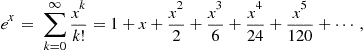 (7.5)
(7.5)
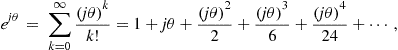 (7.6)
(7.6)
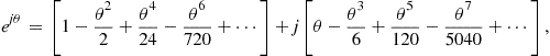 (7.7)
(7.7)
![]() (7.8)
(7.8)
![]() (7.9)
(7.9)
![]() (7.10)
(7.10)
We now examine the phase argument of the sampled data sinusoid. The successive samples of a sampled complex sinusoid are formed as shown in Eq. (7.11) by replacing the continuous argument t with the sample time positions nT as was done in Eq. (7.12). We now note that while the argument of the sampled data sinusoid is dimensionless, the independent variable is no longer “t” with units of seconds but rather “n” with units of sample. This is consistent with the dimension of “T” which of course is s/sample. Consequently the product ![]() has units of (rad/s)
has units of (rad/s) ![]() (s/smpl) or rad/smpl, thus digital frequency is rad/smpl or emphatically the angle change per sample! A more useful version of Eq. (7.12) is obtained by replacing
(s/smpl) or rad/smpl, thus digital frequency is rad/smpl or emphatically the angle change per sample! A more useful version of Eq. (7.12) is obtained by replacing ![]() with
with ![]() as done in Eq. (7.13) and then replace T with
as done in Eq. (7.13) and then replace T with ![]() as was done in Eq. (7.14). We finally replace
as was done in Eq. (7.14). We finally replace ![]() with
with ![]() as was done in Eq. (7.15). Here we clearly see that the parameter
as was done in Eq. (7.15). Here we clearly see that the parameter ![]() has units of rad/smpl, which described the fraction of the circle the argument traverses per successive sample
has units of rad/smpl, which described the fraction of the circle the argument traverses per successive sample
![]() (7.11)
(7.11)
![]() (7.12)
(7.12)
![]() (7.13)
(7.13)
![]() (7.14)
(7.14)
![]() (7.15)
(7.15)
Now suppose we have a sampled sinusoid with sample rate 8-times the sinusoid’s center frequency so that there are 8-samples per cycle. This is equivalent to the sampled sinusoid having a digital frequency of ![]() . We can visualize a spinning phasor rotating 1/8th of the way around the unit circle per sample. Figure 7.12 subplots 1 and 2 show 21 samples of this sinusoid and its spectrum. Note the pair of spectral lines located at
. We can visualize a spinning phasor rotating 1/8th of the way around the unit circle per sample. Figure 7.12 subplots 1 and 2 show 21 samples of this sinusoid and its spectrum. Note the pair of spectral lines located at ![]() on the normalized frequency axis. We can reduce the sample rate of this time series by taking every other sample. The spinning rate for this new sequence is
on the normalized frequency axis. We can reduce the sample rate of this time series by taking every other sample. The spinning rate for this new sequence is ![]() or
or ![]() . The down sampled sequence has doubled its digital frequency. The newly sampled sequence and its spectrum are shown in Figure 7.12 subplots 3 and 4. Note the pair of spectral lines are now located at
. The down sampled sequence has doubled its digital frequency. The newly sampled sequence and its spectrum are shown in Figure 7.12 subplots 3 and 4. Note the pair of spectral lines are now located at ![]() on the normalized frequency axis. We can further reduce the sample rate of by again taking every other sample (or every 4th sample of the original sequence). The spinning rate for this new sequence is
on the normalized frequency axis. We can further reduce the sample rate of by again taking every other sample (or every 4th sample of the original sequence). The spinning rate for this new sequence is ![]() or
or ![]() . The down sampled sequence has again doubled its digital frequency. The newly sampled sequence and its spectrum are shown in Figure 7.12 subplots 5 and 6. Note the pair of spectral lines are now located at
. The down sampled sequence has again doubled its digital frequency. The newly sampled sequence and its spectrum are shown in Figure 7.12 subplots 5 and 6. Note the pair of spectral lines are now located at ![]() on the normalized frequency axis. We once again reduce the sample rate of by taking every other sample (or every 8th sample of the original sequence). The spinning rate for this new sequence is
on the normalized frequency axis. We once again reduce the sample rate of by taking every other sample (or every 8th sample of the original sequence). The spinning rate for this new sequence is ![]() or
or ![]() , but since a
, but since a ![]() rotation is equivalent to no rotation, the spinning phasor appears to be stationary or rotating at 0 rad/smpl. The newly sampled sequence and its spectrum are shown in Figure 7.12 subplots 7 and 8. Note the pair of spectral lines are now located at
rotation is equivalent to no rotation, the spinning phasor appears to be stationary or rotating at 0 rad/smpl. The newly sampled sequence and its spectrum are shown in Figure 7.12 subplots 7 and 8. Note the pair of spectral lines are now located at ![]() which is equivalent to 0 on the normalized frequency axis. Frequency shifts due to sample rate changes are attributed to aliasing. Aliasing enables us to move spectrum from one frequency location to another location without the need for the complex mixers we normally use in a digital down converter to move a spectral span to base-band.
which is equivalent to 0 on the normalized frequency axis. Frequency shifts due to sample rate changes are attributed to aliasing. Aliasing enables us to move spectrum from one frequency location to another location without the need for the complex mixers we normally use in a digital down converter to move a spectral span to base-band.

Figure 7.12 Time series and spectra of sinusoid aliased to new digital frequencies as a result of down-sampling.
Speaking of the standard digital down converter Figure 7.13 presents the primary signal flow blocks based on the DSP emulation of the conventional analog receiver. Figure 7.14 shows the spectra that will be observed at successive output ports of the DDC. We can follow the signal transformations of the DDC by following the spectra in the following description. The top figure shows the spectrum at the output of the analog to digital converter. The second figure shows the spectrum at the output of the quadrature mixer. Here we see the input spectrum has been shifted so that the selected channel band resides at zero frequency. The third figure shows the output of the low-pass filter pair. Here we see that a significant fraction of the input bandwidth has been rejected by the stop band of the low pass filter. Finally, the last figure shows the spectrum after the M-to-1 down sampling that reduced the sample rate in proportion to the reduction in bandwidth performed by the filter. We will always reduce sample rate if we are reducing bandwidth. We have no performance advantage for over satisfying the Nyquist criterion, but incur significant penalties by operating the DSP processors at higher than necessary sample rates.
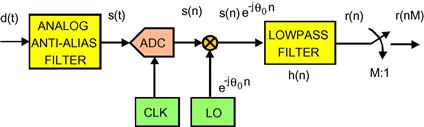
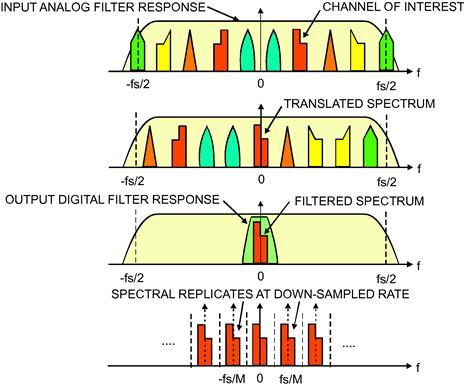
Figure 7.15 presents the primary signal flow blocks based on aliasing the selected band pass span to base-band by reducing the output sample rate of the band pass filter. Figure 7.16 shows the spectra that will be observed at successive output ports of the aliasing DDC. We can follow the signal transformations of the aliasing DDC by following the spectra in the following description. The top figure shows the spectrum at the output of the analog to digital converter. The second figure shows the spectrum of the complex band pass filter and the output spectrum from this filter. The band pass filter is formed by up-converting, by a complex heterodyne, the coefficients of the prototype low pass filter. We note that this filter does not have a mirror image. Analog designers sigh when they see this digital option. The third figure shows the output of the band pass filter pair following the M-to-1 down sampling. If the center frequency of the band is a multiple of the output sample rate the aliased band resides at base band. For the example shown here the center frequency was ![]() above k
above k![]() and since all multiples of
and since all multiples of ![]() alias to base-band, our selected band has aliased to
alias to base-band, our selected band has aliased to ![]() above zero frequency. Finally, the last figure shows the spectrum after the output heterodyne from
above zero frequency. Finally, the last figure shows the spectrum after the output heterodyne from ![]() to base-band. Note that the heterodyne is applied at the low output rate rather than at the input at the high input rate as was done in Figure 7.13.
to base-band. Note that the heterodyne is applied at the low output rate rather than at the input at the high input rate as was done in Figure 7.13.
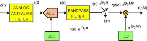
Figure 7.15 Building blocks of aliasing digital down converter with M-to-1 down sampler following filter.
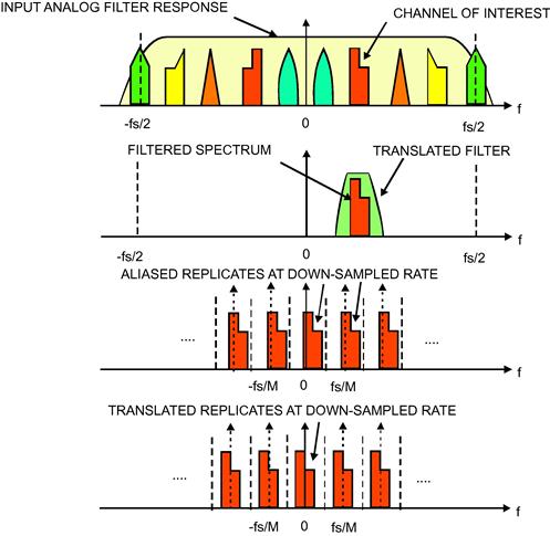
Figure 7.16 Spectra at consecutive points in aliasing digital down converter with down sampling following filter.
Our last section of this preface deals with the equivalency of cascade operators. Here is the core idea. Suppose we have a cascade of two filters, say a low pass filter followed by a derivative filter as shown in Figure 7.17. The filters are linear operators that commute and are distributive. We could reorder the two filters and have the same output from their cascade or we could apply the derivative filter operator to the low pass filter to form a composite filter and obtain the same output as from the cascade. This equivalency is shown in Figure 7.18. The important idea here is that we can filter the input signal and then apply an operator to the filter output or we can apply the operator to the filter and have the altered filter perform both operators to the input signal simultaneously.
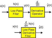

Figure 7.18 Spectrum of cascade filters is same as spectrum of single filter containing combined responses.
Here comes the punch-line! Let us examine the aliasing digital down converter of Figure 7.15 which contains a band pass filter followed by an M-to-1 resampler. This section is redrawn in the upper half of Figure 7.19. If we think about it, this almost silly: Here we compute one output sample for each input sample and then discard M-1 of these samples in the M-to-1 down sampler. Following the lead of the cascade linear operators, the filter and resampler, being equivalent to a composite filter containing the resampler applied to the filter we replace the pair of operators with the composite operator as shown in the lower half of Figure 7.19.
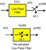
Embedding the M-to-1 resampler in the band pass filter is accomplished by the block diagram shown in Figure 7.20. This filter accepts M inputs, one for each path, and computes 1 output. Thus we do not waste operations computing output sample scheduled to be discarded. An interesting note here is that the complex rotators applied to the prototype low pass filter in Figure 7.15 have been factored out of each arm and are applied once at the output of each path. This means that if the input data is real, the samples are not made complex till they leave the filter. This represents a 2-to-1 savings over the architecture of Figure 7.13 in which the samples are made complex on the way into the filter which means there are 2 filters, one for each path of the complex heterodyne. The alias based DDS with resampler embedded in the filter is not a bad architecture! It computes output samples at the output rate and it only uses one partitioned filter rather than 2. Not bad is understatement! The cherry on top of this dessert is the rotator vector applied to the output of the path filters. This rotator can extract any band from the aliased frequency spans that have aliased to base-band by the resampling operator. If it can extract any band then we have the option of extracting more than one band, and in fact we can extract every band from the output of the partitioned filter. That’s amazing! This filter can service more than one output channel simultaneously; all it needs is additional rotator vectors. As we will see shortly, the single filter structure can service all the channels that alias to base-band and the most efficient bank of rotators is implemented by an M-point IFFT. More to come! Be sure to read on! We have only scratched the surface and the body of material related to multirate filters if filled with many wonderful properties and applications.

1.07.4 Windowing
As specified in the previous section, digital filters can be classified in many ways, starting with the most general frequency domain characteristics such as low pass, high pass, band pass, band stop and finishing with, secondary characteristics such as uniform and non-uniform group delay. We now also know that an important classification is based on the filter’s architectural structure with a primary consideration being that of finite impulse response and infinite impulse response filter. Further sub-classifications, such as canonic forms, cascade forms, lattice forms are primarily driven by consideration of sensitivity to finite arithmetic, memory requirements, ability to pipeline arithmetic, and hardware constraints.
The choice to perform a given filtering task with a recursive or a non-recursive filter is driven by a number of system considerations, including processing resources, clock speed, and various filter specifications. Performance specifications, which include operating sample rate, pass band and stop band edges, pass band ripple, and out-of-band attenuation, all interact to determine the complexity required of the digital filter.
In filters with infinite impulse response each output sample depends on previous input samples and on previous filter output samples. That is the reason for which their practical implementation always requires a feedback loop. Thus, like all feedback based architectures, IIR filters are sensitive to input perturbations that could cause instability and infinite oscillations at the output. However infinite impulse response filters are usually very efficient and require far few multiplications than an FIR filter per output sample. Notice that an IIR filter could have an infinite sequence of output samples even if the input samples become all zeros. It is this characteristic which gives them their name.
Finite impulse response filters use only current and past input samples and none of the filter’s previous output samples to obtain a current output sample value (remember that they are also sometimes referred to as non-recursive filters). Given a finite duration of the input signal, the FIR filter will always have a finite duration of non-zero output samples and this is the characteristic which gives them their name.
The procedure by which the FIR filters calculate the output samples is the convolution of the input sequence with the filter impulse response which is shown in Eq. (7.16)
 (7.16)
where ![]() is the input sequence,
is the input sequence, ![]() is the filter impulse response and M is the number of filter taps. The convolution is nothing but a series of multiplications followed by the addition of the products while the impulse response of a filter is nothing but what the name tells us: it is the time domain view of the filter’s output values when the input is an impulse (a single unity-valued sample preceded and followed by zero-valued samples).
is the filter impulse response and M is the number of filter taps. The convolution is nothing but a series of multiplications followed by the addition of the products while the impulse response of a filter is nothing but what the name tells us: it is the time domain view of the filter’s output values when the input is an impulse (a single unity-valued sample preceded and followed by zero-valued samples).
In the following paragraphs we introduce the basic window design method for FIR filters. Because low pass filtering is the most common filtering task, we will introduce the window design method for low pass FIR filters. However the relationships between filter length and filter specifications and the interactions between filter parameters remain valid for other filter types. Many other techniques can be also used to design FIR filters and, at the end of this section, we will introduce the Remez algorithm, which is one of the most used filter design technique, as well as one of its modified versions which allows us to achieve 1/f type of decay for the out of band side-lobes.
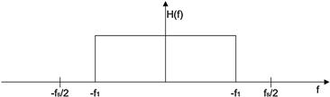
The frequency response of a prototype low pass filter is shown in Figure 7.21. The pass band is seen to be characterized by an ideal rectangle with unity gain between the frequencies ![]() Hz and zero gain elsewhere.
Hz and zero gain elsewhere.
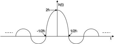
The attraction of the ideal low pass filter H(f) as a prototype is that, from its closed form inverse Fourier transform, we achieve the exact expression for its impulse response h(t) which is shown in Eq. (7.17)
![]() (7.17)
(7.17)
The argument of the ![]() function is always the product of
function is always the product of ![]() , half the spectral support
, half the spectral support ![]() , and the independent variable t. The numerator is periodic and becomes zero when the argument is a multiple of
, and the independent variable t. The numerator is periodic and becomes zero when the argument is a multiple of ![]() . The impulse response of the prototype filter is shown in Figure 7.22. The
. The impulse response of the prototype filter is shown in Figure 7.22. The ![]() filter shown in Figure 7.22 is a continuous function which we have to sample to obtain the prototype sampled data impulse response. To preserve the filter gain during the sampling process we scale the sampled function by the sample rate
filter shown in Figure 7.22 is a continuous function which we have to sample to obtain the prototype sampled data impulse response. To preserve the filter gain during the sampling process we scale the sampled function by the sample rate ![]() . The problem with the sample set of the prototype filter is that the number of samples is unbounded and the filter is non-causal. If we had a finite number of samples, we could delay the response to make it causal and solve the problem. Then our first task is to reduce the unbounded set of filter coefficients to a finite set. The process of pruning an infinite sequence to a finite sequence is called windowing. In this process, a new limited sequence is formed as the product of the finite sequence w(n) and the infinite sequence as shown in Eq. (7.18) where the.∗ operator is the standard MATLAB point-by-point multiply
. The problem with the sample set of the prototype filter is that the number of samples is unbounded and the filter is non-causal. If we had a finite number of samples, we could delay the response to make it causal and solve the problem. Then our first task is to reduce the unbounded set of filter coefficients to a finite set. The process of pruning an infinite sequence to a finite sequence is called windowing. In this process, a new limited sequence is formed as the product of the finite sequence w(n) and the infinite sequence as shown in Eq. (7.18) where the.∗ operator is the standard MATLAB point-by-point multiply
![]() (7.18)
(7.18)
Applying the properties of the Fourier transforms we obtain the expression for the spectrum of the windowed impulse response which is the circular convolution of the Fourier transform of h(n) and w(n).
The symmetric rectangle we selected as our window abruptly turns off the coefficient set at its boundaries. The sampled rectangle weighting function has a spectrum described by the Dirichlet kernel which is the periodic extension of the transform of a continuous time rectangle function. The convolution between the spectra of the prototype filter with the Dirichlet kernel forms the spectrum of the rectangle windowed filter coefficient set. The contribution to the corresponding output spectrum is seen to be the stop band ripple, the transition bandwidth, and the pass band ripple. The pass band and stop band ripples are due to the side-lobes of the Dirichlet kernel moving through the pass band of the prototype filter while the transition bandwidth is due to the main lobe of the kernel moving from the stop band to the pass band of the prototype. A property of the Fourier series is that their truncated version forms a new series exhibiting the minimum mean square (MMS) approximation to the original function. We thus note that the set of coefficients obtained by a rectangle window exhibits the minimum mean square approximation to the prototype frequency response. The problem with MMS approximations in numerical analysis is that there is no mechanism to control the location or value of the error maxima. The local maximum errors are attributed to the Gibbs phenomena, the failure of the series to converge in the neighborhood of a discontinuity. These errors can be objectionably large. A process must now be invoked to control the objectionably high side-lobe levels. We have two ways to approach the problem. First we can redefine the frequency response of the prototype filter so that the amplitude discontinuities are replaced with a specified tapering in the transition bandwidth. In this process, we trade-off the transition bandwidth for side-lobe control. Equivalently, knowing that the objectionable stop band side-lobes are caused by the side-lobes in the spectrum of the window, we can replace the rectangle window with other even symmetric functions with reduced amplitude side-lobe levels. The two techniques, side-lobe control and transition-bandwidth control are tightly coupled. The easiest way to visualize control of the side-lobes is by destructive cancelation between the spectral side-lobes of the Dirichlet kernel associated with the rectangle and the spectral side-lobes of translated and scaled versions of the same kernel. The cost we incur to obtain reduced side-lobe levels is an increase in main lobe bandwidth. Remembering that the window’s two-sided main lobe width is an upper bound to the filter’s transition bandwidth, we can estimate the transition bandwidth of a filter required to obtain a specified side-lobe level. The primary reason we examined windows and their spectral description as weighted Dirichlet kernels was to develop a sense of how we trade the main lobe width of the window for its side-lobe levels and in turn filter transition bandwidth and side-lobe levels. Some windows perform this trade-off of bandwidth for side-lobe level very efficiently while others do not.
The Kaiser-Bessel window is very effective while the triangle (or Fejer) window is not. The Kaiser-Bessel window is in fact a family of windows parameterized over the time-bandwidth product, ![]() , of the window. The main lobe width increases with
, of the window. The main lobe width increases with ![]() while the peak side-lobe level decreases with
while the peak side-lobe level decreases with ![]() . The Kaiser-Bessel window is a standard option in filter design packages such as Matlab and QED-2000.
. The Kaiser-Bessel window is a standard option in filter design packages such as Matlab and QED-2000.
Other filter design techniques include the Remez algorithm [6], sometimes also referred to as the Parks-McClellan or P-M, the McClellan, Parks and Rabiner or MPR, the Equiripple, and the Multiple Exchange algorithm, which found large acceptance in practice. It is a very versatile algorithm capable of designing FIR filters with various frequency responses, including multiple pass band and stop band frequency responses with independent control of ripple levels in the multiple bands. The desired pass band cut off frequencies, the frequencies where the attenuated bands begin and the desired pass band and stop band ripple are given as input parameters to the software which will generate N time domain filter coefficients. N is the minimum number of taps required for the desired filter response and it is selected by using the harris approximation or the Hermann approximation (in Matlab). The problem with the Remez algorithm is that it shows equiripple side-lobes which is not a desirable characteristic. We would like to have a filter frequency response which has a l/f out-of-band decay rate rather than exhibit equiripple. The main reasons for desiring that characteristic are related to system performance. We often build systems comprising a digital filter and a resampling switch. Here the digital filter reduces the bandwidth and is followed by a resampling switch that reduces the output sample commensurate with the reduced output bandwidth. When the filter output is resampled, the low level energy residing in the out-of-band spectral region aliases back into the filter pass band. When the reduction in sample rate is large, there are multiple spectral regions that alias or fold into the pass band. For instance, in a 16-to-l reduction in sample rate, there are 15 spectral regions that fold into the pass band. The energy in these bands is additive and if the spectral density in each band is equal, as it is in an equiripple design, the folded energy level is increased by a factor of sqrt(15). The second reason for which we may prefer FIR filters with l/f side-lobe attenuation as opposed to uniform side-lobes is finite arithmetic. A filter is defined by its coefficient set and an approximation to this filter is realized by a set of quantized coefficients. Given two filter sets ![]() and
and ![]() , the first with equiripple side-lobes, the second with l/f side-lobes, we form two new sets,
, the first with equiripple side-lobes, the second with l/f side-lobes, we form two new sets, ![]() and
and ![]() , by quantizing their coefficients. The quantization process is performed in two steps: first we rescale the filters by dividing with the peak coefficient. Second, we represent the coefficients with a fixed number of bits to obtain the quantized approximations. The zeros of an FIR filter residing on the unit circle perform the task of holding down the frequency response in the stop band. The interval between the zeros contains the spectral side-lobes. When the interval between adjacent zeros is reduced, the amplitude of the side-lobe between them is reduced and when the interval between adjacent zeros is increased the amplitude of the side-lobe between them is increased. The zeros of the filters are the roots of the polynomials
, by quantizing their coefficients. The quantization process is performed in two steps: first we rescale the filters by dividing with the peak coefficient. Second, we represent the coefficients with a fixed number of bits to obtain the quantized approximations. The zeros of an FIR filter residing on the unit circle perform the task of holding down the frequency response in the stop band. The interval between the zeros contains the spectral side-lobes. When the interval between adjacent zeros is reduced, the amplitude of the side-lobe between them is reduced and when the interval between adjacent zeros is increased the amplitude of the side-lobe between them is increased. The zeros of the filters are the roots of the polynomials ![]() and
and ![]() . The roots of the polynomials formed by the quantized set of coefficients differ from the roots of the non-quantized polynomials. For small changes in coefficient size, the roots exhibit small displacements along the unit circle from their nominal positions. The amplitude of some of the side-lobes must increase due to this root shift. In the equiripple design, the initial side-lobes exactly meet the designed side-lobe level with no margin for side-lobe increase due to root shift caused by coefficient quantization. On the other hand, the filter with 1/f side-lobe levels has plenty of margin for side-lobe increase due to root shift caused by coefficient quantization.
. The roots of the polynomials formed by the quantized set of coefficients differ from the roots of the non-quantized polynomials. For small changes in coefficient size, the roots exhibit small displacements along the unit circle from their nominal positions. The amplitude of some of the side-lobes must increase due to this root shift. In the equiripple design, the initial side-lobes exactly meet the designed side-lobe level with no margin for side-lobe increase due to root shift caused by coefficient quantization. On the other hand, the filter with 1/f side-lobe levels has plenty of margin for side-lobe increase due to root shift caused by coefficient quantization.
More details on the modified Remez algorithm can be found in [6].
1.07.5 Basics on multirate filters
Multirate filters are digital filters that contain a mechanism to increase or decrease the sample rate while processing input sampled signals. The simplest multirate filter performs integer up sampling of 1-to-M or integer down sampling of Q-to-1. By extension, a multirate filter can employ both up sampling and down sampling in the same process to affect a rational ratio sample rate change of M-to-Q. More sophisticated techniques exist to perform arbitrary and perhaps slowly time varying sample rate changes. The integers M and Q may be selected to be the same so that there is no sample rate change between input and output but rather an arbitrary time shift or phase offset between input and output sample positions of the complex envelope. The sample rate change can occur at a single location in the processing chain or can be distributed over several subsections.
Conceptually, the process of down sampling can be visualized as a two-step progression indicated in Figure 7.23. There are three distinct signals associated with this procedure. The process starts with an input series ![]() that is processed by a filter
that is processed by a filter ![]() to obtain the output sequence
to obtain the output sequence ![]() with reduced bandwidth. The sample rate of the output sequence is then reduced Q-to-1 to a rate commensurate with the reduced signal bandwidth. In reality the processes of bandwidth reduction and sample rate reduction are merged in a single process called multirate filter. The bandwidth reduction performed by the digital filter can be a low-pass or a band-pass process.
with reduced bandwidth. The sample rate of the output sequence is then reduced Q-to-1 to a rate commensurate with the reduced signal bandwidth. In reality the processes of bandwidth reduction and sample rate reduction are merged in a single process called multirate filter. The bandwidth reduction performed by the digital filter can be a low-pass or a band-pass process.

In a dual way, the process of up sampling can be visualized as a two-step process as indicated in Figure 7.24. Here too there are three distinct time series. The process starts by increasing the sample rate of an input series ![]() by resampling it 1-to-M. The zero-packed time series with M-fold replication of the input spectrum is processed by a filter
by resampling it 1-to-M. The zero-packed time series with M-fold replication of the input spectrum is processed by a filter ![]() to reject the spectral replicas and output the sequence
to reject the spectral replicas and output the sequence ![]() with the same spectrum as the input sequence but sampled at M times higher sample rate. In reality the processes of sample rate increase and selected bandwidth rejection are also merged in a single process again called multirate filtering.
with the same spectrum as the input sequence but sampled at M times higher sample rate. In reality the processes of sample rate increase and selected bandwidth rejection are also merged in a single process again called multirate filtering.

The presented structures are the most basic forms of multirate filters; in the following we present more complicated multirate architecture models. In particular we focus on the polyphase decomposition of a prototype filter which is very efficient when embedded in multirate structures. We also propose the derivation, step by step, of both the polyphase down converter and up converter channelizers. These are the two standard engines that we will modify for designing a novel polyphase channelizer that better fits the needs of the future software defined radio.
1.07.6 From single channel down converter to standard down converter channelizer
The derivation of the standard polyphase channelizer begins with the issue of down converting a single frequency band, or channel, located in a multi channel frequency division multiplexed (FDM) input signal whose spectrum is composed of a set of M equally spaced, equal bandwidth channels, as shown in Figure 7.25. Note that this signal has been band limited by analog filters and has been sampled at a sufficiently high sample rate to satisfy the Nyquist criterion for the full FDM bandwidth.
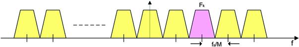
Figure 7.25 Spectrum of multichannel input signal, processing task: extract complex envelope of selected channel.
We have many options available for down converting a single channel; The standard processing chain for accomplishing this task is shown in Figure 7.26. This structure performs the standard operations of down converting a selected frequency band with a complex heterodyne, low pass filtering to reduce the output signal bandwidth to the channel bandwidth, and down sampling to a reduced rate commensurate with the reduced bandwidth. The structure of this processor is seen to be a digital signal processor implementation of a prototype analog I-Q down converter. We mention that the down sampler is commonly referred to as a decimator, a term that means to destroy one sample every tenth. Since nothing is destroyed and nothing happens in tenths, we prefer, and will continue to use, the more descriptive name, down sampler.
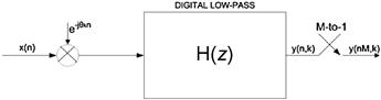
The output data from the complex mixer is complex, hence it is represented by two time series, ![]() and
and ![]() . The filter with real impulse response
. The filter with real impulse response ![]() is implemented as two identical filters, each processing one of the quadrature time series. The convolution process between a signal and a filter is often performed by simply multiply and sum operations between signal data samples and filter coefficients extracted from two sets of addressed memory registers. In this form of the filter, one register set contains the data samples while the other contains the coefficients that define the filter impulse response. By using the equivalency theorem, which states that the operations of down conversion followed by a low-pass filter are equivalent to the operations of band-pass filtering followed by a down conversion, we can exchange the positions of the filter and of the complex heterodyne achieving the block diagram shown in Figure 7.27.
is implemented as two identical filters, each processing one of the quadrature time series. The convolution process between a signal and a filter is often performed by simply multiply and sum operations between signal data samples and filter coefficients extracted from two sets of addressed memory registers. In this form of the filter, one register set contains the data samples while the other contains the coefficients that define the filter impulse response. By using the equivalency theorem, which states that the operations of down conversion followed by a low-pass filter are equivalent to the operations of band-pass filtering followed by a down conversion, we can exchange the positions of the filter and of the complex heterodyne achieving the block diagram shown in Figure 7.27.

Note here that the up converted filter, ![]() , is complex and as such its spectrum resides only on the positive frequency axis without a negative frequency image. This is not a common structure for an analog prototype because of the difficulty of forming a pair of analog quadrature filters exhibiting a 90° phase difference across the filter bandwidth. The closest equivalent structure in the analog world is the filter pair used in image-reject mixers and even there, the phase relationship is maintained by a pair of complex heterodynes.
, is complex and as such its spectrum resides only on the positive frequency axis without a negative frequency image. This is not a common structure for an analog prototype because of the difficulty of forming a pair of analog quadrature filters exhibiting a 90° phase difference across the filter bandwidth. The closest equivalent structure in the analog world is the filter pair used in image-reject mixers and even there, the phase relationship is maintained by a pair of complex heterodynes.
Applying the transformation suggested by the equivalency theorem to an analog prototype system does not make sense since it doubles the required hardware. We would have to replace a complex scalar heterodyne (two mixers) and a pair of low-pass filters with a pair of band-pass filters, containing twice the number of reactive components, and a full complex heterodyne (four mixers). If it makes no sense to use this relationship in the analog domain, why does it make sense in the digital world? The answer is found in the fact that we define a digital filter as a set of weights stored in the coefficient memory. Thus, in the digital world, we incur no cost in replacing the pair of low-pass filters ![]() required in the first option with the pair of band-pass filters
required in the first option with the pair of band-pass filters ![]() and
and ![]() required for the second one. We accomplish this task by a simple download to the coefficient memory.
required for the second one. We accomplish this task by a simple download to the coefficient memory.
An interesting historical perspective is worth noting here. In the early days of wireless, radio tuning was accomplished by sliding a narrow band filter to the center frequency of the desired channel to be extracted from the FDM input signal. These radios were known as tuned radio frequency (TRF) receivers. The numerous knobs on the face of early radios adjusted reactive components of the amplifier chain to accomplish the tuning process. Besides the difficulty in aligning multiple tuned stages, shifting the center frequency of the amplifier chain often initiated undesired oscillation due to the parasitic coupling between the components in the radio. Edwin Howard Armstrong, an early radio pioneer, suggested moving the selected channel to the fixed frequency filter rather than moving the filter to the selected channel. This is known as the superheterodyne principle, a process invented by Armstrong in 1918 and quickly adopted by David Sarnoff of the Radio Corporation of America (RCA) in 1924. Acquiring exclusive rights to Armstrong’s single-tuning dial radio invention assured the commercial dominance of RCA in radio broadcasting as well the demise of hundreds of manufacturers of TRF radio receivers. It seems we have come full circle. We inherited from Armstrong a directive to move the desired spectrum to the filter and we have readily applied this legacy to DSP-based processing. We are now proposing that, under appropriate conditions, it makes more sense to move the filter to the selected spectral region. We still have to justify the full complex heterodyne required for the down conversion at the filter output rather than at the filter input, which is done in the subsequent paragraphs.
Examining Figure 7.27, we note that following the output down conversion, we perform a sample rate reduction in which we retain one sample out of M-samples. Because we find it useless to down convert the samples we discard in the next down sample operation, we move the down sampler before the down converter achieving the demodulator scheme shown Figure 7.28. We note in this figure that also the time series of the complex sinusoid has been down sampled. The rotation rate of the sampled complex sinusoid is ![]() and
and ![]() radians per sample at the input and output of the M-to-1 resampler respectively. This change in observed rotation rate is due to aliasing. When aliased, a sinusoid at one frequency or phase slope appears at another phase slope due to the resampling.
radians per sample at the input and output of the M-to-1 resampler respectively. This change in observed rotation rate is due to aliasing. When aliased, a sinusoid at one frequency or phase slope appears at another phase slope due to the resampling.
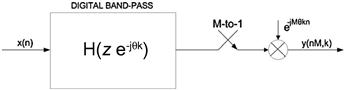
We now invoke a constraint on the sampled data center frequency of the down converted channel. We choose center frequencies ![]() , which will alias to DC as a result of down sampling to
, which will alias to DC as a result of down sampling to ![]() . This condition is assured if
. This condition is assured if ![]() is congruent to
is congruent to ![]() , which occurs when
, which occurs when ![]() , or more specifically, when
, or more specifically, when ![]() . The modification to Figure 7.28 to reflect this provision is seen in Figure 7.29. The constraint, that the center frequencies be limited to integer multiples of the output sample rate, assures aliasing to base-band by the sample rate change. When a channel aliases to base-band because the resampling operation the corresponding resampled heterodyne defaults to a unity-valued scalar, which consequently is removed from the signal processing path.
. The modification to Figure 7.28 to reflect this provision is seen in Figure 7.29. The constraint, that the center frequencies be limited to integer multiples of the output sample rate, assures aliasing to base-band by the sample rate change. When a channel aliases to base-band because the resampling operation the corresponding resampled heterodyne defaults to a unity-valued scalar, which consequently is removed from the signal processing path.

Note that if the center frequency of the aliased signal is offset by ![]() from a multiple of the output sample rate, the aliased signal will reside at an offset of
from a multiple of the output sample rate, the aliased signal will reside at an offset of ![]() from zero frequency at base-band and a complex heterodyne, or base-band converter, is needed to shift the signal by the residual
from zero frequency at base-band and a complex heterodyne, or base-band converter, is needed to shift the signal by the residual ![]() offset. This base-band mixer operates at the output sample rate rather than at the input sample rate for a conventional down converter. We can consider this required final mixing operation as a post conversion task and allocate it to the next processing block.
offset. This base-band mixer operates at the output sample rate rather than at the input sample rate for a conventional down converter. We can consider this required final mixing operation as a post conversion task and allocate it to the next processing block.
The spectral effect of the signal processing performed by the structure in Figure 7.29 is shown in Figure 7.30. The savings realized by this form of down conversion is due to the fact that we no longer require a quadrature oscillator or the pair of input mixers to effect the required frequency translation.

Applying again the idea that it is useless to filter those samples that will be lately discarded by the down sampler we apply the noble identity to exchange the operations of filtering and down sampling. The noble identity states that a filter processing every Mth input sample followed by an output M-to-1 down sampler is the same as an input M-to-1 down sampler followed by a filter processing every input sample. Its interpretation is that the M-to-l down sampled time series from a filter processing every ![]() input sample presents the same output by first down sampling the input by M-to-1, to discard the samples not used by the filter when computing the retained output samples, and then operating the filter on only the retained input samples. The noble identity works because samples of delay at the input clock rate is the same interval as one-sample delay at the output clock rate.
input sample presents the same output by first down sampling the input by M-to-1, to discard the samples not used by the filter when computing the retained output samples, and then operating the filter on only the retained input samples. The noble identity works because samples of delay at the input clock rate is the same interval as one-sample delay at the output clock rate.
At this point, with only a filter followed by a resampler, we can apply the polyphase decomposition to the filter and separate it into M-parallel paths for achieving the standard M-path polyphase down converter channelizer. In order to make the understanding process easier for the reader, we first perform the polyphase decomposition of a low-pass prototype filter and then we extend the results to the band-pass filter case. Equation (7.19) represents the z transform of a digital low-pass prototype filter ![]()
 (7.19)
In order to achieve the polyphase partition of ![]() , we rewrite the sum in Eq. (7.19), as shown in Eq. (7.20), partitioning the one-dimensional array of weights in a two-dimensional array. In this mapping we load an array by columns but process it by rows. The partition forms columns of length M containing M successive terms in the original array, and continues to form adjacent M-length columns until we account for all the elements of the original one-dimensional array
, we rewrite the sum in Eq. (7.19), as shown in Eq. (7.20), partitioning the one-dimensional array of weights in a two-dimensional array. In this mapping we load an array by columns but process it by rows. The partition forms columns of length M containing M successive terms in the original array, and continues to form adjacent M-length columns until we account for all the elements of the original one-dimensional array
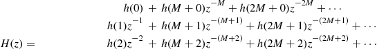 (7.20)
![]()
We note that the first row of the two-dimensional array is a polynomial in ![]() , which we will denote
, which we will denote ![]() a notation to be interpreted as an addressing scheme to start at index 0 and increment in strides of length M. The second row of the same array, while not a polynomial in
a notation to be interpreted as an addressing scheme to start at index 0 and increment in strides of length M. The second row of the same array, while not a polynomial in ![]() , is made into one by factoring the common term
, is made into one by factoring the common term ![]() and then identifying this row as
and then identifying this row as ![]() . It is easy to see that each row of the two-dimensional array described by Eq. (7.8) can be written as
. It is easy to see that each row of the two-dimensional array described by Eq. (7.8) can be written as ![]() achieving the more compact form as shown in Eq. (7.9) where r is the row index which is coincident with the path index
achieving the more compact form as shown in Eq. (7.9) where r is the row index which is coincident with the path index
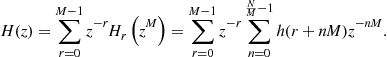 (7.21)
The block diagram depicting the M-path polyphase decomposition of the resampled low-pass filter of Eq. (7.21) is depicted in Figure 7.31.

At this point, in the structure depicted in Figure 7.31, we can pull the resampler on the left side of the adder and down sample the separate filter outputs performing the sum only for the retained filter output samples. With the resamplers at the output of each filter we can invoke again the noble identity and place them at the input of each filter.
The resamplers operate synchronously, all closing at the same clock cycle. When the switches are closed, the signal delivered to the filter on the top path is the current input sample. The signal delivered to the filter one path down is the content of the one stage delay line, which, of course, is the previous input sample. Similarly, as we traverse the successive paths of the M-path partition, we find upon switch closure, that the ![]() path receives a data sample delivered k samples ago. We conclude that the interaction of the delay lines in each path with the set of synchronous switches can be likened to an input commutator that delivers successive samples to successive arms of the M-path filter. This interpretation is shown in Figure 7.32 which depicts the final structure of the polyphase decomposition of a low-pass prototype filter.
path receives a data sample delivered k samples ago. We conclude that the interaction of the delay lines in each path with the set of synchronous switches can be likened to an input commutator that delivers successive samples to successive arms of the M-path filter. This interpretation is shown in Figure 7.32 which depicts the final structure of the polyphase decomposition of a low-pass prototype filter.

Figure 7.32 M-path partition of prototype low-pass filter with input delays and M-to-1 resamples replaced by input commutator.
At this point we can easily achieve the band-pass polyphase partition from the low-pass partition by applying the frequency translation property of the z-Transform that states the following.
If
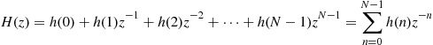
and

then
![]()
By using this property and replacing in Eq. (7.21) each ![]() with
with ![]() , where
, where ![]() , we achieve
, we achieve
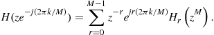 (7.22)
The complex scalars ![]() attached to each path of the M-path filter can be placed anywhere along the path. We choose to place them after the down sampled path filter segments
attached to each path of the M-path filter can be placed anywhere along the path. We choose to place them after the down sampled path filter segments ![]() . This change is shown in Figure 7.33 that depicts the standard polyphase filter bank used for down converting a single channel. The computation of the time series obtained from the output summation in Figure 7.33 is shown in Eq. (7.23). Here, the argument
. This change is shown in Figure 7.33 that depicts the standard polyphase filter bank used for down converting a single channel. The computation of the time series obtained from the output summation in Figure 7.33 is shown in Eq. (7.23). Here, the argument ![]() reflects the down sampling operation, which increments through the time index in strides of length M, delivering every Mth sample of the original output series. The variable
reflects the down sampling operation, which increments through the time index in strides of length M, delivering every Mth sample of the original output series. The variable ![]() is the nMth sample from the filter segment in the rth path, and
is the nMth sample from the filter segment in the rth path, and ![]() is the nMth time sample of the time series from the
is the nMth time sample of the time series from the ![]() center frequency. Remember that the down converted center frequencies located at integer multiples of the output sample frequency alias to zero frequency after the resampling operation. Note that the output
center frequency. Remember that the down converted center frequencies located at integer multiples of the output sample frequency alias to zero frequency after the resampling operation. Note that the output ![]() is computed as a phase coherent summation of the output series
is computed as a phase coherent summation of the output series ![]() . This phase coherent sum is, in fact, an inverse discrete Fourier transform of the M-path outputs, which can be likened to beam forming the output of the path filters
. This phase coherent sum is, in fact, an inverse discrete Fourier transform of the M-path outputs, which can be likened to beam forming the output of the path filters
 (7.23)
The beam forming perspective offers an interesting insight to the operation of the resampled down converter system we have just examined; the reasoning proceeds as follows: the commutator delivering consecutive samples to the M input ports of the M-path filter performs a down sampling operation. Each port of the M-path filter receives data at 1/Mth of the input rate. The down sampling causes the M-to-1 spectral folding, effectively translating the ![]() multiples of the output sample rate to base-band. The alias terms in each path of the M-path filter exhibit unique phase profiles due to their distinct center frequencies and the time offsets of the different down sampled time series delivered to each port. These time offsets are, in fact, the input delays shown in Figure 7.31 and Eq. (7.3). Each of the aliased center frequency experiences a phase shift shown in Eq. (7.24) equal to the product of its center frequency and the path time delay.
multiples of the output sample rate to base-band. The alias terms in each path of the M-path filter exhibit unique phase profiles due to their distinct center frequencies and the time offsets of the different down sampled time series delivered to each port. These time offsets are, in fact, the input delays shown in Figure 7.31 and Eq. (7.3). Each of the aliased center frequency experiences a phase shift shown in Eq. (7.24) equal to the product of its center frequency and the path time delay.
![]() (7.24)
(7.24)
The phase shifters of the IDFT perform phase coherent summations, very much like that performed in narrowband beam forming, extracting from the myriad of aliased time series, the alias with the particular matching phase profile. This phase sensitive summation aligns contributions from the desired alias to realize the processing gain of the coherent sum while the remaining alias terms, which exhibit rotation rates corresponding to the M roots of unity, are destructively canceled in the summation. The inputs to the M-path filter are not narrowband, and phase shift alone is insufficient to cause the destructive cancelation over the full bandwidth of the undesired spectral contributions. Continuing with our beam-forming perspective, to successfully separate signals with unique phase profiles due to the input commutator delays, we must perform the equivalent of time-delay beam forming. The M-path filters, obtained by M-to-1 down sampling of the prototype low-pass filter supply the required time delays. The M-path filters are approximations to all-pass filters, exhibiting, over the channel bandwidth, equal ripple approximation to unity gain and the set of linear phase shifts that provide the time delays required for the time-delay beam-forming task. The filter achieves this property by virtue of the way it is partitioned. Each of the M-path filters, ![]() , for instance, with weights
, for instance, with weights ![]() , is formed by starting with an initial offset of r samples and then incrementing in strides of M samples. The initial offsets, unique to each path, are the source of the different linear phase-shift profiles. It is because of the different linear phase profiles, that the filter partition is known as polyphase filter. An useful perspective is that the phase rotators following the filters perform phase alignment of the band center for each aliased spectral band while the polyphase filters perform the required differential phase shift across these same channel bandwidths.
, is formed by starting with an initial offset of r samples and then incrementing in strides of M samples. The initial offsets, unique to each path, are the source of the different linear phase-shift profiles. It is because of the different linear phase profiles, that the filter partition is known as polyphase filter. An useful perspective is that the phase rotators following the filters perform phase alignment of the band center for each aliased spectral band while the polyphase filters perform the required differential phase shift across these same channel bandwidths.

When the polyphase filter is used to down convert and down sample a single channel, the phase rotators are implemented as external complex products following each path filter. When a small number of channels are being down converted and down sampled, appropriate sets of phase rotators can be applied to the filter stage outputs and summed to form each channel output. Therefore the most advantageous applications of that structure are those in which the number of channels to be down converted becomes sufficiently large. Sufficiently large means on the order of ![]() . Since the phase rotators following the polyphase filter stages are the same as the phase rotators of an IDFT, we can use the IDFT to simultaneously apply the phase shifters for all the channels we wish to extract from the aliased signal set. This is reminiscent of phased-array beam forming. For computational efficiency, the IFFT algorithm implements the IDFT.
. Since the phase rotators following the polyphase filter stages are the same as the phase rotators of an IDFT, we can use the IDFT to simultaneously apply the phase shifters for all the channels we wish to extract from the aliased signal set. This is reminiscent of phased-array beam forming. For computational efficiency, the IFFT algorithm implements the IDFT.
The complete structure of a standard M-path polyphase down converter channelizer is shown in Figure 7.34.

Figure 7.34 Standard polyphase down converter channelizer: commutator, M-path polyphase filter and M-point IFFT.
To summarize: in this structure the commutator performs an input sample rate reduction by commutating successive input samples to selected paths of the M-path filter. Sample rate reduction occurring prior to any signal processing causes spectral regions residing at multiples of the output sample rate to alias to base-band. The partitioned M-path filter performs the task of aligning the time origins of the offset sampled data sequences delivered by the input commutator to a single common output time origin. This is accomplished by the all-pass characteristics of the ![]() -path filter sections that apply the required differential time delay to the individual input time series. The IDFT performs the equivalent of a beam-forming operation; the coherent summation of the time-aligned signals at each output port with selected phase profiles. The phase coherent summation of the outputs of the
-path filter sections that apply the required differential time delay to the individual input time series. The IDFT performs the equivalent of a beam-forming operation; the coherent summation of the time-aligned signals at each output port with selected phase profiles. The phase coherent summation of the outputs of the ![]() -path filters separates the various aliases residing in each path by constructively summing the selected aliased frequency components located in each path, while simultaneously destructively canceling the remaining aliased spectral components.
-path filters separates the various aliases residing in each path by constructively summing the selected aliased frequency components located in each path, while simultaneously destructively canceling the remaining aliased spectral components.
We conclude the reasoning on the standard M-path down converter channelizer by stating that it simultaneously performs the following three basic operations: sample rate reduction, due to the input commutator; bandwidth reduction, due to the M-path partitioned filter weights and Nyquist zone selection, due to the IFFT block.
In the following, in order to facilitate the understanding process for the reader, we show some figures, which are results of Matlab simulation, to support the theoretical reasoning of the previous paragraphs. The example concerns a 6-path down converter channelizer that performs 6-to-1 down sampling. In particular Figure 7.35 shows the impulse response and the frequency response of the low-pass prototype filter used for the polyphase partition.

Figure 7.36 shows the impulse responses of the zero-packed filter on each arm of the 6-path polyphase partition while Figure 7.37 shows the spectra corresponding to the filters of Figure 7.36. It is evident from this figure that the zero packing process has the effect of producing spectral copies of the filter frequency response.
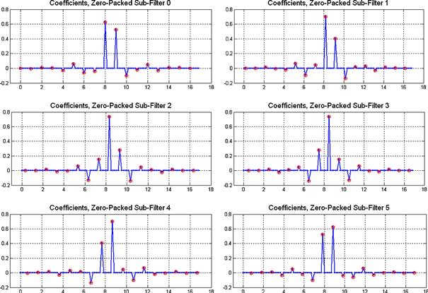

In Figure 7.38 we show the phase of each spectral copy of the zero packed prototype filter on each arm of the partition. In this figure the phases of the spectral copies of each arm are overlaid and each line of the plot corresponds to a specific arm in the partition.
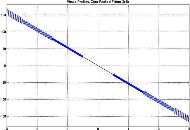
In Figure 7.39 the same phase profiles of Figure 7.38 are de-trended, zoomed, and made causal.

In Figure 7.40 the 3-D view of the filter spectral copies, with their phase profiles, is shown for each path, while, in Figure 7.41, the final result of the channelization process is shown, again in a 3-D fashion.

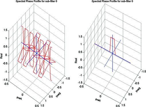
1.07.6.1 From single channel up converter to standard up converter channelizer
The standard M-path up converter channelizer that performs 1-to-M up sampling while up converting the input time series is derived from the basic structure, shown in Figure 7.11, of a single channel interpolator formed of an up sampler followed by an appropriate low-pass filter. In this configuration, the up sampler converts the Nyquist interval, which is the observable frequency span, from the input sample rate to a span M times wider, which is the output sample rate. The 1-to-M up sampler zero packs the input time series, effectively decreasing the distance between the input samples without modifying the spectral content of the series. The wider Nyquist interval, spanning M input Nyquist intervals, presents M spectral copies of the input spectrum to the low-pass filter. The amplitude of each of the M copies is ![]() of the amplitude of the input signal spectrum. When a low-pass filter is scaled so that the peak coefficient is unity, the filter exhibits a processing gain inversely proportional to its fractional bandwidth. Thus, as the filter eliminates the M-1 spectral copies, reducing the bandwidth by a factor of 1/M, the filter gain precisely compensates for the attenuation of the input spectra due to the zero packing of the input series.
of the amplitude of the input signal spectrum. When a low-pass filter is scaled so that the peak coefficient is unity, the filter exhibits a processing gain inversely proportional to its fractional bandwidth. Thus, as the filter eliminates the M-1 spectral copies, reducing the bandwidth by a factor of 1/M, the filter gain precisely compensates for the attenuation of the input spectra due to the zero packing of the input series.
We start the modifications of this basic architecture by observing that the zero valued samples of the zero-packed input time series do not contribute to the weighted sums formed at the filter output. Since they do not contribute, there is no need to perform the product and sum from the input data registers containing the known zero-valued samples. Since only the non-zero packed samples contribute to the filter output, we can track their location in the filter and perform the weighted sum only from the register locations containing these samples. These locations are separated by M sample values, and their position shifts through the filter as each new zero-valued input is presented to the input of the filter. Keeping track of the coefficient stride and the position of each coefficient set is automatically performed by the polyphase partition of the filter which is represented in Eq. (7.25). This equation describes the filter as a sum of successively delayed sub-filters with coefficients separated by the stride of M samples. Equation (7.26) is a compact representation of Eq. (7.25) where the rth stage ![]() of the polyphase filter is formed by the coefficient set that starts at index r and increments in steps of length M
of the polyphase filter is formed by the coefficient set that starts at index r and increments in steps of length M
 (7.25)
 (7.26)
The pictorial form of the filter in the M-path polyphase partition is shown in Figure 7.42. This structure enables the application of the noble identity in which we slide the resampler through the filter and replace the M units of delay at the output clock rate with one unit of delay at the input clock rate. Note that the resampler cannot slide through the delays ![]() following each filter segment
following each filter segment ![]() .
.
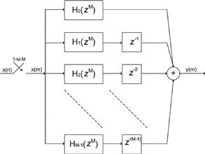
The resamplers following the separate filter stages up sample each time series by a factor of M, and the delays in each arm shift each resulting time series at different time increments so that only one non-zero time sample is presented to the summing junction at each output time. Thus, rather than performing the sum with multiple zeros, we can simply point to the arm that sequentially supplies the non-zeros samples. The output commutator, shown in Figure 7.43, performs this selective access. Figure 7.42 represents the standard polyphase interpolator or up sampler. Due to the low-pass nature of the filter on which the polyphase decomposition has been applied, this structure does not perform the up conversion of the interpolated signal yet. Its output is the same low-pass input spectrum with a sample rate that is M times higher than the input sample rate.
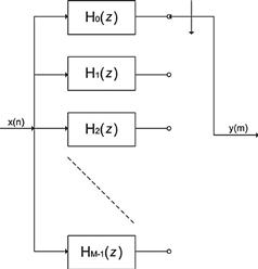
We recall here that the purpose of the interpolation process is to increase the input sample rate while translating the input spectrum to a higher carrier frequency. If used in a communication system, such a structure directly translates the input signal to an intermediate frequency (IF), and then outputs the digital IF signal via a single DAC. This option reduces the system costs by using a single DAC and a band-pass filter to replace the standard base-band process requiring matched DACs, matched low-pass filters, matched balanced mixers, and a quadrature oscillator to form the IF frequency band.
In the structure of Figure 7.24, the 1-to-M interpolating process zero packed the input data giving us access to M spectral copies of the input time series. The spectral copies reside at multiples of the input sample rate. The low-pass filter rejected the spectral copies, retrieving only the base-band copy centered at DC that is then sent through a digital up converter for translation to the desired center frequency. It is possible to perform the spectral translation as a part of the interpolation process when the desired center frequency coincides with one of the multiples of the input sample rate. Rather than extracting the spectral copy at base-band from the replicated set of spectra and then translating it by means of a complex heterodyne, we can directly extract one of the spectral copies by using a band-pass filter as opposed to a low-pass filter. The band-pass filter is simply an up converted version of the low-pass filter ![]() with weights shown in Eq. (7.27). Here the center frequency is interpreted as the
with weights shown in Eq. (7.27). Here the center frequency is interpreted as the ![]() multiple of
multiple of ![]() of the output sample rate.
of the output sample rate.
![]() (7.27)
(7.27)
The z-transform of the band-pass filter ![]() , is shown in Eq. (7.28)
, is shown in Eq. (7.28)
 (7.28)
The z-transform of the polyphase decomposition of this filter is shown in Eq. (7.29). Here we see that the length M stride in coefficient index due to the 1-to-M resampling aliases the phase rotators in the polyphase filter stages to DC and hence has no effect on the polyphase weights. The phase rotator does, however, have a contribution related to the delay associated with each arm of the partition. The output commutator process absorbs the delays while the phase rotators are applied to each arm to obtain the spectral translation as a part of the interpolation.
 (7.29)
The polyphase filter that accomplishes the task of simultaneous interpolation and up conversion to the ![]() Nyquist zone is shown in Figure 7.44. This engine up samples and up converts, by aliasing, a single narrowband channel to a particular center frequency which is a multiple of the input sample rate. By noticing, as we did in the previous section of this chapter for the dual down converter channelizer, that the phase rotators applied in each arm are the coefficients of an inverse discrete Fourier transform it is easy to generalize this structure to the standard multichannel polyphase up converter channelizer by applying an IDFT block at the input of the filter bank.
Nyquist zone is shown in Figure 7.44. This engine up samples and up converts, by aliasing, a single narrowband channel to a particular center frequency which is a multiple of the input sample rate. By noticing, as we did in the previous section of this chapter for the dual down converter channelizer, that the phase rotators applied in each arm are the coefficients of an inverse discrete Fourier transform it is easy to generalize this structure to the standard multichannel polyphase up converter channelizer by applying an IDFT block at the input of the filter bank.
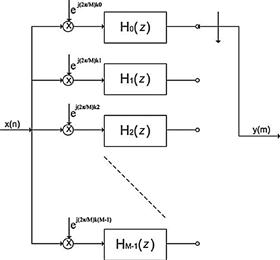
Figure 7.44 Structure of 1-to-M polyphase interpolator with phase rotators for selecting the spectrum centered in Mth nyquist zone.
Figure 7.45 shows the complete structure of the standard M-path polyphase up converter channelizer. It is composed of an M point IDFT block, an M-path partitioned filter and an output commutator. In this structure, we enter the M-channel process at the IDFT block and leave the process by the output commutator. The M-point IDFT performs two simultaneous tasks; an initial up sampling of 1-to-M, forming an M-length vector for each input sample ![]() and further imparts a complex phase rotation of k cycles in M-samples on the up sampled output vector. It generates a weighted sum of complex vectors containing integer number of cycles per M-length vector. The polyphase filter forms a sequence of column coefficient weighted, MATLAB’s dot-multiply, versions of these complex spinning vectors. The sum of these columns, formed by the set of inner products in the polyphase partitioned filter, is the shaped version of the up converted M-length vector output from the IFFT. On each output port of this engine we find the input base-band channel aliased to the specific Nyquist zone with a new sampling rate that is commensurate with its reduced bandwidth.
and further imparts a complex phase rotation of k cycles in M-samples on the up sampled output vector. It generates a weighted sum of complex vectors containing integer number of cycles per M-length vector. The polyphase filter forms a sequence of column coefficient weighted, MATLAB’s dot-multiply, versions of these complex spinning vectors. The sum of these columns, formed by the set of inner products in the polyphase partitioned filter, is the shaped version of the up converted M-length vector output from the IFFT. On each output port of this engine we find the input base-band channel aliased to the specific Nyquist zone with a new sampling rate that is commensurate with its reduced bandwidth.
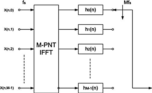
Figure 7.45 Polyphase up converter channelizer: M-point IFFT, M-path polyphase filter and commutator.
A closing comment on both the standard polyphase up converter and down converter channelizer is that the operations of sampling rate change, spectral shaping and Nyquist zone selection are completely independent of each other. The channel bandwidth, the channel spacing and the output sampling rate do not have necessarily to be equal but they can be all modified according to the applications.
1.07.7 Modifications of the standard down converter channelizer—M:2 down converter channelizer
In the standard polyphase down converter channelizer shown in Figure 7.34 the channel bandwidth ![]() , the channel spacing
, the channel spacing ![]() , and the sampling frequency
, and the sampling frequency ![]() are fixed to be equal.
are fixed to be equal.
This configuration could represent a good choice when the polyphase channelizer is used for communication systems. In these kind of applications, in fact, an output sample rate matching the channel spacing is sufficient to avoid adjacent channel cross talk since the two-sided bandwidth of each channel is less than the channel spacing. An example of a signal that would require this mode of operation is the Quadrature Amplitude Modulation (QAM) channels of a digital cable system. In North America, the channels are separated by 6 MHz centers and operate with square-root cosine tapered Nyquist-shaped spectra with 18% or 12% excess bandwidth, at symbol rates of approximately 5.0 MHz. The minimum sample rate required of a cable channelizer to satisfy the Nyquist criterion would be 6.0 MHz (The European cable plants have channel spacing of 8.0 MHz and symbol rates of 7.0 MHz). The actual sample rate would likely be selected as a multiple of the symbol rate rather than as a multiple of the channel spacing. Systems that channelize and form samples of the Nyquist-shaped spectrum often present the sampled data to an interpolator to resample the time series collected at bandwidth-related Nyquist rate to a rate offering two samples per symbol or twice symbol rate. For the TV example just cited, the 6 Ms/s, 5 MHz symbol signal would have to be resampled by 5/3 to obtain the desired 10 Ms/s. This task is done quite regularly in the communication receivers and it may represent a significant computational burden. It would be appropriate if we could avoid the external interpolation process by modifying the design of the standard polyphase channelizer for directly providing us the appropriate output sampling frequency.
Many others applications desire channelizers in which the output sampling frequency is not equal to the channel spacing and the channel bandwidth. The design of software defined radio receiver and transmitter is only one of them. Another one can be found in [8].
We have concluded the previous section mentioning that the channel spacing, the channel bandwidth and the output sampling frequency of the polyphase channelizer are completely independent of each other and that they can be arbitrary selected based on the application. Figure 7.46 shows some possible options in which the channel bandwidth, the output sampling rate and the channel spacing of the channelizer are not equal. In this chapter, for the purpose of designing flexible radio architectures, the third option, when the selected low-pass prototype filter is a Nyquist filter (perfect reconstruction filter), results to be the most interesting one.

In this section of the chapter we derive the reconfigured version of the standard down converter channelizer that is able to perform the sample rate change from the input rate ![]() to the output sampling rate
to the output sampling rate ![]() maintaining both the channel spacing and the channel bandwidth equal to
maintaining both the channel spacing and the channel bandwidth equal to ![]() . Similar reasoning can be applied for implementing different selections.
. Similar reasoning can be applied for implementing different selections.
Note that the standard down converter channelizer is critically sampled when the channel spacing and the channel bandwidth are both equal to ![]() and when the output sample rate is also equal to
and when the output sample rate is also equal to ![]() . This particular choice, in fact, causes the transition band edges of the channelizer filters to alias onto itself which would prevent us from further processing the signals when they are arbitrarily located in the frequency domain which is the case of software radio. This problem can be visualized in the upper example depicted in Figure 7.46.
. This particular choice, in fact, causes the transition band edges of the channelizer filters to alias onto itself which would prevent us from further processing the signals when they are arbitrarily located in the frequency domain which is the case of software radio. This problem can be visualized in the upper example depicted in Figure 7.46.
For the record, we remind that a polyphase filter bank can be operated with an output sample rate which can be any rational ratio of the input sample rate. With minor modifications the filter can be operated with totally arbitrary ratios between input and output sample rates. This is true for the sample rate reduction imbedded in a polyphase receiver as well as for the sample rate increase embedded in a polyphase modulator.
We have control on the output sampling rate of the down converter channelizer by means of the input commutator that delivers input data samples to the polyphase stages. We normally deliver M successive input samples to the M-path filter starting at port M-1 and progressing up the stack to port 0 and by doing so we deliver M inputs per output which means to perform an M-to-1 down sampling operation. To obtain the desired (M/2)-to-1 down sampling, we have to modify the input commutator in a way that it delivers M/2 successive input samples starting at port (M/2)-1 and progressing up the stack to port 0. We develop and illustrate the modifications with the aid of Figures 7.47–7.50.
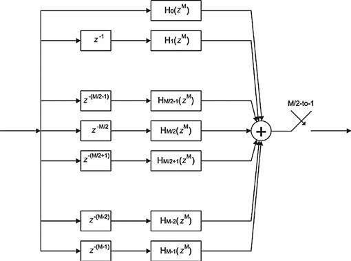
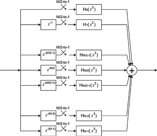

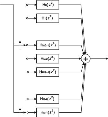
Figure 7.47 represents the polyphase M-path filter partition shown in Eq. (7.9) with an M/2-to-1 rather than the conventional M-to-1 down sample operation after the output summing junction. We need it in order to perform the desired sampling rate change.
In Figure 7.48 we apply the noble identity to the polyphase paths by pulling the M/2-to-1 down sampler through the path filters which converts the polynomials in ![]() operating at the high input rate to polynomials in
operating at the high input rate to polynomials in ![]() operating at the lower output rate.
operating at the lower output rate.
Figure 7.49 shows the second application of the noble identity in which we again take the M/2-to-1 down samplers through the ![]() parts of the input path delays for the paths in the second or bottom half of the path set.
parts of the input path delays for the paths in the second or bottom half of the path set.
In Figure 7.50 the M/2-to-1 down samplers switch and their delays are replaced with a two pronged commutator that delivers the same sample values to path inputs with the same path delay. Here we also merged the ![]() delays in the lower half of filter bank with their path filters.
delays in the lower half of filter bank with their path filters.
Figure 7.51 shows and compares the block diagrams of the path filters in the upper and lower half of this modified polyphase partition.

When the input commutator is so designed, the M/2 addresses to which the new M/2 input samples are delivered have to be first vacated by their former contents, the M/2 previous input samples. All the samples in the two-dimensional filter undergo a serpentine shift of M/2 samples with the M/2 samples in the bottom half of the first column sliding into the M/2 top addresses of the second column while the M/2 samples in the top half of the second column slide into the M/2 addresses in the bottom half of the second column, and so on. This is equivalent to performing a linear shift through the prototype one-dimensional filter prior to the polyphase partition. In reality, we do not perform the serpentine shift but rather perform an addressing manipulation that swaps two memory banks. This is shown in Figure 7.52.

Figure 7.52 Data memory loading for successive M/2-point sequences in an M-stage polyphase channelizer.
After each M/2-point data sequence is delivered to the partitioned M-stage polyphase filter, in the standard channelizer configuration, the outputs of the M stages are computed and conditioned for delivery to the M-point IFFT. What we need to do at this point is the time alignment of the shifting time origin of the input samples in the M-path filter with the stationary time origin of the phase rotator outputs of the IFFT. We can understand the problem by visualizing, in Figure 7.53, a single cycle of a sine wave extending over M samples being inserted in the input data register, the first column of the polyphase filter in segments of length M/2. We can assume that the data in the first M/2 addresses are phase aligned with the first M/2 samples of a single cycle of the sine wave offered by the IFFT.
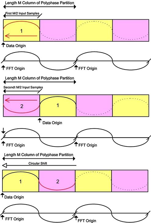
When the second M/2 input samples are delivered to the input data register the first M/2 input samples shift to the second half of the M-length array. Its original starting point is now at address M/2 but the IFFT’s origin still resides at address 0. The shift of the origin causes the input sine wave in the register to have the opposing phase of the sine wave formed by the IFFT; in fact the data shifting into the polyphase filter stages causes a frequency dependent phase shift of the form shown in Eq. (7.30). The time delay due to shifting is nT where n is the number of samples, and T is the time interval between samples. The frequencies of interest are integer multiple k of 1/Mth of the sample rate ![]() . Substituting these terms in Eq. (7.30) and canceling terms, we obtain the frequency dependent phase shift shown in Eq. (7.31). From this relationship we see that for time shifts n equal to multiples of M, as demonstrated in Eq. (7.32), the phase shift is a multiple of
. Substituting these terms in Eq. (7.30) and canceling terms, we obtain the frequency dependent phase shift shown in Eq. (7.31). From this relationship we see that for time shifts n equal to multiples of M, as demonstrated in Eq. (7.32), the phase shift is a multiple of ![]() and contributes zero offset to the spectra observed at the output of the IFFT. The M-sample time shift is the time shift applied to the data in the normal use of the polyphase filter. Now suppose that the time shift is M/2 time samples. When substituted in Eq. (7.31) we find, as shown in Eq. (7.33), as frequency dependent phase shift of
and contributes zero offset to the spectra observed at the output of the IFFT. The M-sample time shift is the time shift applied to the data in the normal use of the polyphase filter. Now suppose that the time shift is M/2 time samples. When substituted in Eq. (7.31) we find, as shown in Eq. (7.33), as frequency dependent phase shift of ![]() from which we conclude that odd-indexed frequency terms experience a phase shift of
from which we conclude that odd-indexed frequency terms experience a phase shift of ![]() radians for each successive N/2 shift of input data
radians for each successive N/2 shift of input data
![]() (7.30)
(7.30)
![]() (7.31)
(7.31)
![]() (7.32)
(7.32)
![]() (7.33)
(7.33)
This ![]() radiants phase shift is due to the fact that the odd-indexed frequencies alias to the half sample rate when the input signal is down sampled by M/2. What we are observing is the sinusoids with an odd number of cycles in the length M array alias to the half sample rate when down sampled M/2-to-1. Note that, when down sampled M/2-to-1, the sinusoids with an even number of cycles in the length M array alias to DC. We can compensate for the alternating signs in successive output samples by applying the appropriate phase correction to the spectral data as we extract successive time samples from the odd-indexed frequency bins of the IFFT. The phase correction here is trivial, but for other down-sampling ratios, the residual phase correction would require a complex multiply at each transform output port. Alternatively, since time delay imposes a frequency dependent phase shift, we can use time shifts to cancel the frequency dependent phase shifts. We accomplish this by applying a circular time shift of
radiants phase shift is due to the fact that the odd-indexed frequencies alias to the half sample rate when the input signal is down sampled by M/2. What we are observing is the sinusoids with an odd number of cycles in the length M array alias to the half sample rate when down sampled M/2-to-1. Note that, when down sampled M/2-to-1, the sinusoids with an even number of cycles in the length M array alias to DC. We can compensate for the alternating signs in successive output samples by applying the appropriate phase correction to the spectral data as we extract successive time samples from the odd-indexed frequency bins of the IFFT. The phase correction here is trivial, but for other down-sampling ratios, the residual phase correction would require a complex multiply at each transform output port. Alternatively, since time delay imposes a frequency dependent phase shift, we can use time shifts to cancel the frequency dependent phase shifts. We accomplish this by applying a circular time shift of ![]() samples to the vector of samples prior to their presentation to the IFFT. As in the case of the serpentine shift of the input data, the circular shift of the polyphase filter output data is implemented as an address-manipulated data swap. This data swap occurs on alternate input cycles and a simple two-state machine determines for which input cycle the output data swap is applied. This is shown in Figure 7.54.
samples to the vector of samples prior to their presentation to the IFFT. As in the case of the serpentine shift of the input data, the circular shift of the polyphase filter output data is implemented as an address-manipulated data swap. This data swap occurs on alternate input cycles and a simple two-state machine determines for which input cycle the output data swap is applied. This is shown in Figure 7.54.

Figure 7.54 Cyclic shift of input data to IFFT to absorb phase shift due to linear time shift of data through polyphase filter.
The complete structure of the modified version of the M-to-2 down converter channelizer with the input data buffer and the circular data buffer is shown in Figure 7.55.
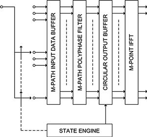
For brevity of notation, we avoid reporting here all the dual mathematical derivations that led at the final structure of the modified up converter channelizer. We briefly explain its block diagram in the next subsection.
1.07.7.1 Modifications of the standard up converter channelizer—2:M up converter channelizer
Dual reasoning drives us to the reconfigured version of the M-path polyphase up converter channelizer that is able to perform the sample rate change from ![]() to
to ![]() maintaining both the channel spacing and the channel bandwidth equal to
maintaining both the channel spacing and the channel bandwidth equal to ![]() . The choice of using a 2-to-M up sampler avoids the difficulty of having the sample rate that precisely matches the two sided bandwidth of the input signals as well as permitting a shorter length prototype channelizer filter due to an allowable wider transition bandwidth. In this chapter we briefly derive its block diagram that is shown in Figure 7.45. More details on this structure can be found in [6,8,9]. We develop and illustrate the modifications with the aid of Figures 7.56–7.61. In these figures we do not consider the IFFT block because, for now, it does not affect our reasoning. Moreover we will introduce it later motivating the reason for which it is important to include a circular buffer in the design of the modified up converter channelizer.
. The choice of using a 2-to-M up sampler avoids the difficulty of having the sample rate that precisely matches the two sided bandwidth of the input signals as well as permitting a shorter length prototype channelizer filter due to an allowable wider transition bandwidth. In this chapter we briefly derive its block diagram that is shown in Figure 7.45. More details on this structure can be found in [6,8,9]. We develop and illustrate the modifications with the aid of Figures 7.56–7.61. In these figures we do not consider the IFFT block because, for now, it does not affect our reasoning. Moreover we will introduce it later motivating the reason for which it is important to include a circular buffer in the design of the modified up converter channelizer.
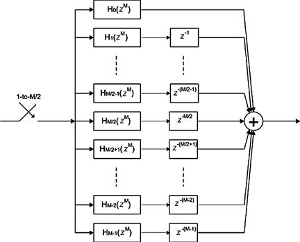
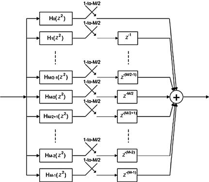


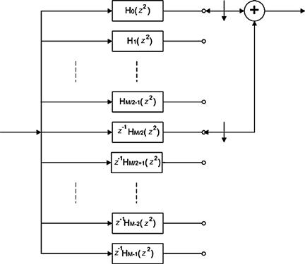
Figure 7.56 presents the structure of the M-path filter implementation of the polyphase partition shown in Eq. (7.7). Note the 1-to-M/2 up-sample operation at the input port normally described as the zero-packing process. In Figure 7.57 we apply the noble identity to the polyphase paths and pull the 1-to-M/2 up sampler through the path filters which convert the polynomials in ![]() operating at the high output rate to polynomials in
operating at the high output rate to polynomials in ![]() operating at the low input rate. Note that the paths are now polynomials in
operating at the low input rate. Note that the paths are now polynomials in ![]() rather than
rather than ![]() as is the normal mode that we identify as the dual of the maximally decimated filter bank.
as is the normal mode that we identify as the dual of the maximally decimated filter bank.
Figure 7.58 shows the second application of the noble identity in which we again take the 1-to-M/2 up sampler through the ![]() part of the output path delays for the paths in the second or bottom half of the path set. The resultant delay,
part of the output path delays for the paths in the second or bottom half of the path set. The resultant delay, ![]() , now operating at the input clock rate, is then interchanged with its path filter as shown in Figure 7.59.
, now operating at the input clock rate, is then interchanged with its path filter as shown in Figure 7.59.
In Figure 7.60 the 1-to-M/2 up samplers switch and their delays are replaced with a pair of commutators that add the path outputs with the same path delay. Finally, in Figure 7.61 we fold the single delay in front of the lower set of path filters into the path filter. After having changed the output sampling rate of the polyphase channelizer, the final modification we need to introduce is the time alignment of the phase rotators from the input IFFT and the shifted time origin in the M-path filter.
From Figure 7.62, we note the locations of the non-zero coefficients in the polynomials in ![]() and conclude that the input sine wave only contributes to the output time samples in the path filters located in the upper half of the path set. When the next scaled sine wave output from the IFFT is inserted in the first column of the path filter memory, the previous scaled sine wave is shifted one column in the memory and it will now contribute to the output time samples from the filter paths in the lower half of the path filter set. The problem is that the sine wave samples in the lower half of the path filter set have opposite polarity of the sine wave samples in the upper half of the path filter set. The samples from the two half filter sets are added and to do so they must have the same phase. We note that this alternating sign effect only occurs for the odd indexed IFFT frequency bins which have an odd number of cycles per interval.
and conclude that the input sine wave only contributes to the output time samples in the path filters located in the upper half of the path set. When the next scaled sine wave output from the IFFT is inserted in the first column of the path filter memory, the previous scaled sine wave is shifted one column in the memory and it will now contribute to the output time samples from the filter paths in the lower half of the path filter set. The problem is that the sine wave samples in the lower half of the path filter set have opposite polarity of the sine wave samples in the upper half of the path filter set. The samples from the two half filter sets are added and to do so they must have the same phase. We note that this alternating sign effect only occurs for the odd indexed IFFT frequency bins which have an odd number of cycles per interval.

An alternate description of the sign reversal is that in the M/2 resampling of the modified M-path filter the even indexed frequencies alias to multiples of the input sample rate and the odd indexed frequencies alias to odd multiples of the half sample rate.
We recall here that there are two methods for performing the phase alignment of the successive output vectors from the IFFT. In the first method we simply invert the input phase of successive input samples to the odd indexed IFFT bins. In the second method, recognizing that equivalency of phase shift and time delay for sinusoids, on alternate outputs from the IFFT we apply an M/2 circular shift to its output buffer prior to delivering the phase aligned vector to the path filter memory. This end around shift of the output buffer occurs during the data transfer in memory and requires no additional manipulation of the time samples.
Figure 7.63 shows the complete block diagram of the modified M-path up converter channelizer. In this engine, the input commutator delivers the samples to the M-point IFFT. It applies the complex phase rotation to the separate base-band input signals as well as performs the initial 1-to-M up sampling of the input samples. The circular output buffer performs the correct data offset of the two M/2 point halves of the IFFT output vector to maintain phase alignment with the M/2 channelizer output vector. The complex sinusoid output by the IFFT always defines its time origin as the initial sample of its output vector. The output of the polyphase filter exhibits a time origin that shifts due to the M/2 time sample shift embedded in the output commutator. The M/2 time sample shift of the output time series causes sinusoids with an odd number of cycles in the length M array to alternate sign on successive shifts. The alternating sign is the reason that the odd indexed frequency bins up convert to a frequency ![]() rather than frequency index k. Rather than reverse phase alternate input samples to the odd indexed IFFT bins we perform an M/2 point circular shift of alternate M-length vectors from the IFFT for applying the correct phase alignment to all frequencies simultaneously.
rather than frequency index k. Rather than reverse phase alternate input samples to the odd indexed IFFT bins we perform an M/2 point circular shift of alternate M-length vectors from the IFFT for applying the correct phase alignment to all frequencies simultaneously.

The polyphase down converter and up converter channelizers shown in Figures 7.55 and 7.63 respectively are the key elements of the proposed receiver and transmitter structures that we present in the following sections. Because of the signal processing tasks they handle, in the following, we refer to them as analysis and synthesis channelizers respectively.
1.07.8 Preliminaries on software defined radios
The 20th century saw the explosion of hardware defined radio as a means of communicating all forms of data, audible and visual information over vast distances. These radios have little or no software control. Their structures are fixed in accordance with the applications; the signal modulation formats, the carrier frequencies and bandwidths are only some of the factors that dictate the radio structures. The smallest change to one of these parameters could imply a replacement of the entire radio system. A consequence of this is, for example, the fact that a television receiver purchased in France does not work in England. The reason, of course, is that the different geographical regions employ different modulation standards for the analog TV as well as for digital TV. Then, the citizens cannot use the same TV for receiving signals in both countries; they need to buy a new television for each country in which they decide to live. Sometimes, even if the communication devices are designed for the same application purposes and they work in the same geographical area, they are not able to communicate between each other. One of the most evident examples of this is that the city police car radio cannot communicate with the city fire truck radio, or with the local hospital ambulance radio even if they have the common purpose of helping and supporting the citizen. Also, the city fire truck radio cannot communicate with the county fire truck radio, or with the radios of the fire truck operated by the adjacent city, or by the state park service, or the international airport. None of these services can communicate with the National Guard, or with the local Port Authority, or with the local Navy base, or the local Coast Guard base, or the US Border Patrol, or US Customs Service. In an hardware defined radio, if we decide to change one of the parameters of the transmitted signal, like bandwidth or carrier frequency (for example because the carrier frequency we want to use is the only one available at that particular moment), we need to change the transmitter. On the other side, every time we want to receive a signal having different bandwidth or center frequency, we need to change the receiver. Hardware defined transmitter and receiver devices are not flexible at all; we must modify their structure every time we change even one of the transmitting and receiving signal parameters.
In 1991, Joe Mitola coined the term software defined radio. It was referred to a class of reprogrammable (and reconfigurable) devices. At that time it was not clear at which level the digitization should occur to define a radio as software but the concept sounded pretty interesting, and the dream of building a completely reconfigurable radio device involved scientists from all over the world. Today the exact definition of software defined radio is still controversial, and no consensus exists about the level of reconfigurability needed to qualify a radio as software.
Figure 7.64 shows, in a simple block diagram, all the possible places in which the digitization can occur in a radio receiver. The exact dual block diagram can be portrayed for the radio transmitter. Current radios, often referred to as digital but sometimes referred as software defined radios (depending on their particular structure), after shifting the signals to intermediate frequency, digitize them and assign all the remaining tasks to a digital signal processor. One of the main reasons for shifting the signals to intermediate frequency, before digitizing them, is to reduce their maximum frequency so that a smaller number of samples can be taken for preserving the information content.

Figure 7.64 Simple block diagram indicating all the possible places in which the digitization can occur in a radio receiver.
Implementation of ideal software radios requires digitization at the antenna, allowing complete flexibility in the digital domain. Then it requires both the design of a flexible and efficient DSP-based structure and the design of a completely flexible radio frequency front-end for handling a wide range of carrier frequencies, bandwidths and modulation formats. These issues have not been exploited yet in the commercial systems due to technology limitations and cost considerations.
As pointed out in the previous section, in a current software defined radio receiver the signals are digitized in intermediate frequency bands. The receiver employs a super heterodyne frequency down conversion, in which the radio frequency signals are picked up by the antenna along with other spurious, unwanted signals (noise and interferences), filtered, amplified with a low noise amplifier and mixed with a local oscillator to shift it to intermediate frequency. Depending on the application, the number of stages of this operation may vary. Digitizing the signal in the IF range eliminates the last analog stage in the conventional hardware defined radios in which problems like carrier offset and imaging are encountered. When sampled, digital IF signals give spectral replicas that can be placed accurately near the base-band frequency, allowing frequency translation and digitization to be carried out simultaneously. Digital filtering and sample rate conversion are often needed to interface the output of the ADC to the processing hardware to implement the receiver. Likewise, on the transmitter side, digital filtering and sample rate conversion are often necessary to interface the digital hardware, that creates the modulated waveforms, to the digital to analog converter. Digital signal processing is usually performed in radio devices using field programmable gate arrays (FPGAs), or application specific integrated circuits (ASICs).
Even if the dream of building a universal radio is still far away, current software defined radio architectures are quite flexible, in the sense that they usually down convert to IF a collection of signals and, after sampling, they are able to shift these signals to base-band via software. Changes in the signal bandwidths and center frequencies are performed by changing some parameters of the digital data section. The flexibility of such a structure can be improved by moving the analog to digital converter closest to the receiver antenna. By digitizing the signals immediately after (and before in the transmitter) the antenna, which is the ideal software radio case, the down conversion (and up conversion) processes are performed completely in software and the radio acquires the capability of changing its personality, possibly in real-time, guaranteeing a desired quality of service (QoS). The digitization after the receiver antenna, in fact, allows service providers to upgrade the infrastructure and market new services quickly. It promises multi-functionality, global mobility, ease of manufacture, compactness and power efficiency. The flexibility in hardware architectures combined with flexibility in software architectures, through the implementation of techniques such as object oriented programming, can provide software radio also with the ability to seamlessly integrate itself into multiple networks with widely different air and data interfaces.
1.07.9 Proposed architectures for software radios
A digital transmitter accepts binary input sequences and outputs radio frequency amplitude and phase modulated wave shapes. The digital signal processing part of this process starts by accepting b-bit words from a binary source at input symbol rate. These words address a look-up table that outputs gray coded ordered pairs, i.e., I-Q constellation points, that control the amplitude and phase of the modulated carrier. The I-Q pair is input to DSP-based shaping filters that form 1-to-4 up sampled time series designed to control the wave shape and limit the base-band modulation bandwidth. The time series from the shaping filter are further up sampled by a pair of interpolating filters to obtain a wider spectral interval between spectral replicas of the sampled data. The interpolated data are then heterodyned by a digital up converter to a convenient digital intermediate frequency and then moved from the sampled data domain to the continuous analog domain by a digital to analog converter and analog IF filter. Further analog processing performs the spectral transformations required to couple the wave shape to the channel.
On the other side of the communication chain, a digital receiver has to perform the tasks of filtering, spectral translation and analog to digital conversion to reverse the dual tasks performed at the transmitter. The receiver must also perform a number of other tasks absent in the transmitter for estimating the unknown parameters of the received signal such as amplitude, frequency and timing alignment. It samples the output of the analog IF filter and down converts the intermediate frequency centered signal to base-band with a digital down converter (DDC). The base-band signal is down sampled by a decimating filter and finally processed in the matched filter to maximize the signal-to-noise ratio (SNR) of the samples presented to the detector. The DSP portion of this receiver includes carrier alignment, timing recovery, channel equalization, automatic gain control, SNR estimation, signal detection, and interference suppression blocks. In order to suppress the undesired artifacts introduced by the analog components, the receiver also incorporates a number of digital signal processing compensating blocks.
Figure 7.65 shows the first tier processing block diagrams of a typical digital transmitter-receiver chain. The depicted transmitter is designed for sending, one per time, signals having fixed bandwidths at precisely located center frequencies. On the other hand, the depicted receiver is also designed for down converting to base-band fixed bandwidth signals having fixed center frequencies. Therefore, the goal of a cognitive radio is quite different: cognitive transmitter and receiver should be completely flexible. The transmitter has, in fact, to be able to simultaneously up convert, at desired center frequencies, which are selected based on the temporary availability of the radio spectrum, a collection of signals having arbitrary bandwidths. It should also be able to decompose a signal in spectral fragments when a sufficiently wide portion of the radio spectrum is not available for transmission. Of course no energy loss has to occur in the partitioning process. A cognitive receiver has to be able to simultaneously down convert the transmitted signal spectra wherever they are positioned in the frequency domain and whatever bandwidths they have. Also it should have the capability of recognizing spectral segments belonging to the same information signal and recompose them, after the base-band translation, without energy losses. It could be possible to reach this goal by using the current technology but the cost would be very high: for every signal we want to transmit we have to replicate the digital data section of both the transmitter and the receiver. The more signals we have to simultaneously up and down convert, the more sampled data sections we need to implement! Also, it is not possible, by using the current technology, to fragment a single signal, transmit its spectral partitions using the temporary available spectral holes and to perfectly recombine them at the receiver. Today the transmission happens under the constraint that the available space in the radio spectrum is large enough to accommodate the entire bandwidth of the signal to be transmitted.

In the next sections of this chapter, we present novel channelizers to simultaneously up and down convert arbitrary bandwidth signals randomly located in the frequency domain. Differently from the previous contents of this document, from this point onwards the presented material reproduces the results of the authors’ research on software defined radio design, thus it is new. The proposed architectures can be used for the transmitter and for the receiver devices of a cognitive radio respectively. By using them we avoid the need to replicate the sampled data sections for simultaneously transmitting and receiving more signals with arbitrary bandwidths over multiple desired center frequencies. We also gain the capability to partition the signal spectra before transmitting them and to perfectly reassemble them in the receiver after the base-band shifting.
The core of the proposed transmitter structure is the variant of the standard M-path polyphase up converter channelizer that is able to perform 2-to-M up sampling while shifting, by aliasing, all the channels to desired center frequencies. It has been presented in Section 1.07.5 of this same chapter. In the following we use the term synthesis channelizer for referring to this structure. This name has been given for the tasks that this structure accomplishes when embedded in a SDR transmitter. When the input signals have bandwidths wider than the synthesis channelizer bandwidth they are pre-processed through small down converter channelizers that disassemble the signals’ bandwidths into reduced bandwidth sub-channels which are matched to the base-line synthesis channelizer bandwidths. Complex sampled frequency rotators are used to offset the signal spectra by arbitrary fractions of the sample frequency before processing them through the channelizers. This is necessary for the completely arbitrary center frequency positioning of the signals.
On the other side the variation of the standard M-path down converter channelizer, presented in Section 1.07.6, represents the key element of the proposed receiver. It is able to perform M-to-2 down sampling while simultaneously down converting, by aliasing, all the received signal spectra having arbitrary bandwidths. In the following, we refer to this structure as analysis channelizer. Post-processing channelizers, that are a smaller version of the synthesis channelizer composing the transmitter, are used for reassembling, from the analysis channelizer base-line channels, signal bandwidths wider than the analysis channelizer channel bandwidth. Possible residual frequency offsets can be easily solved with the aid of a digital complex heterodyne while a post-analysis block performs further channelization, when it is required, for separating signal spectra falling in the same channelizer channel after the analysis processing.
1.07.9.1 Proposed digital down converter architecture
The standard M-path polyphase down converter channelizer is able to shift to base-band, by aliasing, the input signals that are exactly located on the channel’s center frequencies, kfc, where ![]() . In this engine the center frequencies of the channels are integer multiples of the channelizer output sampling frequency as well as the channelizer channel bandwidth.
. In this engine the center frequencies of the channels are integer multiples of the channelizer output sampling frequency as well as the channelizer channel bandwidth.
We recall here that the standard M-path down sampling channelizer simultaneously down converts, by aliasing, from fixed center frequencies to base-band, M bands narrower than the channelizer channel bandwidth. If ![]() are the center frequencies of the input spectra, where
are the center frequencies of the input spectra, where ![]() are the arbitrary frequency offsets from the channel center frequencies,
are the arbitrary frequency offsets from the channel center frequencies, ![]() , after the down conversion process the output spectra will be shifted by the same offset from DC, i.e., the down converted signals will be centered at the frequency locations
, after the down conversion process the output spectra will be shifted by the same offset from DC, i.e., the down converted signals will be centered at the frequency locations ![]() because the polyphase down converter channelizer only compensates the
because the polyphase down converter channelizer only compensates the ![]() frequency terms. It is unable to compensate the frequency offsets,
frequency terms. It is unable to compensate the frequency offsets, ![]() , that are responsible for the arbitrary center frequency positioning of the input signals. The frequency offset compensation is one of the motivations for which we need to add further processing blocks in the digital down converter design when it is intended to be used in a software radio receiver. Other issues, like receiver resolution, base-band reassembly of wide bandwidths and arbitrary interpolation of the base-band shifted signals need to be considered too. All these issues are addressed and solved in the following paragraphs.
, that are responsible for the arbitrary center frequency positioning of the input signals. The frequency offset compensation is one of the motivations for which we need to add further processing blocks in the digital down converter design when it is intended to be used in a software radio receiver. Other issues, like receiver resolution, base-band reassembly of wide bandwidths and arbitrary interpolation of the base-band shifted signals need to be considered too. All these issues are addressed and solved in the following paragraphs.
We also recall here that the standard M-to-1 down converter channelizer with the channel spacing and channel bandwidth equal to the output sampling frequency is critically sampled (see upper plot of Figure 7.29). In order to use it in a cognitive radio receiver, we need to modify it, redesigning the channel spacing, channel bandwidth, and output sampling frequency. We presented one of these modifications in Section 1.07.5, where the M-to-2 down converter channelizer has been derived. Also the selection of the low-pass prototype filter is an important issue that has to be addressed in order to avoid energy losses while the signal is processed.
Figure 7.66 shows the complete block diagram of the proposed down converting chain. The input signal is processed, at first, by an analysis channelizer which is the modified version of the standard M-to-1 down converter channelizer presented in Section 1.07.5. By performing an M/2-to-1 down sampling of the input time series this engine simultaneously shifts all the aliased channels to base-band presenting an output sampling rate that is twice the sample rate of the standard M-to-1 channelizer. Nyquist filters are used, as low-pass prototype, for avoiding energy losses while processing the signals. They are briefly described in one the next subsections. The interested reader can find more details on Nyquist filter design in [6].
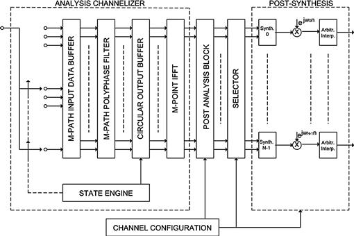
Figure 7.66 Block diagram of the proposed down converter; analysis down converter channelizer, post analysis block, synthesis up converter channelizers, complex frequency rotators and arbitrary interpolators.
Note that if more signals or even spectral fragments belonging to different signals, are channelized in the same channel, further processing is needed to separate them at the output of the analysis down converter. The extra filtering process is performed in the post-analysis block that is connected to a channel configuration block that provides the receiver with the necessary information about the input signal bandwidths and center frequencies. Different options can be implemented for simplifying the design of the post-analysis block. One of the possible options is to decrease the bandwidth of the perfect reconstruction prototype low-pass filter and to increase the number of points of the IFFT block in the analysis channelizer. By designing the channel spacing and bandwidth to accommodate the most likely expected signal width we minimize the possibility of having more than one signal in each channel. It is also possible to modify the analysis channelizer for having a more convenient frequency positioning of the aliased channels. The optimal choice, of course, depends on the receiver application and on the workload requirements.
At the output of the analysis channelizer, most of the signals with bandwidths narrower than the channel bandwidth are already down converted by means of the channelization process. However the spectra wider than the channel bandwidth, or the spectra that, as a consequence of the arbitrary center frequency positioning, are processed by two or more adjacent channels, have been fragmented and their segments have all been aliased to the first Nyquist zone; these segments need to be recomposed before being translated to DC. The recomposition of spectral fragments is the task performed by the synthesis channelizers. They have been presented in Section 9.5.1 and their block diagram is depicted in Figure 7.59. These are small 2-to-![]() polyphase up converters in which the IFFT size,
polyphase up converters in which the IFFT size, ![]() , is properly chosen in order to span the bandwidth of the nth received signal spectrum. We summarize the reason for including the synthesizers in our design in this way: at the output of the M-to-2 analysis channelizer all the signals have been down sampled and their spectra, or their spectral fragments, have been translated to the first Nyquist zone by the channelizing process. In order to reassemble the segments into a wider bandwidth super channel, the time series from each segment must be up sampled and frequency shifted to their appropriate positions so that they can be added together for forming the time series corresponding to the wider bandwidth assembled signal.
, is properly chosen in order to span the bandwidth of the nth received signal spectrum. We summarize the reason for including the synthesizers in our design in this way: at the output of the M-to-2 analysis channelizer all the signals have been down sampled and their spectra, or their spectral fragments, have been translated to the first Nyquist zone by the channelizing process. In order to reassemble the segments into a wider bandwidth super channel, the time series from each segment must be up sampled and frequency shifted to their appropriate positions so that they can be added together for forming the time series corresponding to the wider bandwidth assembled signal.
At the end of the down conversion and up conversion processes, all the received spectra have been frequency translated and, when necessary, recomposed in the first Nyquist zone. The analysis down converter channelizer shifted to base-band the signal spectra and their fragments, that are exactly centered on its channels’ center frequencies. This engine was not able to compensate the frequency offsets deriving from the arbitrary frequency positioning of the received signals.
The frequency offset compensation task is accomplished by the complex frequency rotators that follow the small up converter synthesizers. They are connected with the channel configuration block that provides them proper information about the signal center frequencies.
Once the signals are perfectly centered at DC, arbitrary interpolators are used to adjust their sampling rate to provide us exactly two samples per symbol needed for the further processing stages that are performed in the digital receiver.
1.07.9.1.1 Post-analysis block and synthesis up converter channelizers
At the output of the analysis channelizer all the channels have been aliased to base-band. As a consequence of that, the channelized segments of the received spectrum have been aliased to the first Nyquist zone (see Figure 7.61).
The following three options, that cover all the possible cases of bandwidths positioning in the channelized spectrum, have to be considered and solved, by further processing the analysis channelizer outputs, in order to achieve, at the end of the analysis-synthesis chain, all the received bands shifted to base-band:
1. The aliased base-band channel could contain only one signal spectrum whose bandwidth is narrower than the channel bandwidth. The carrier frequency of the signal, generally, does not coincide with the center frequency of the channel.
2. The aliased base-band channel could contain two or more spectra, or also their fragments, belonging to different signals. These spectra are arbitrarily positioned in the channel bandwidth.
3. The base-band channel could contain only one spectral fragment belonging to one of the received signals which has bandwidth larger than the channel bandwidth.
In the first option, at the output of the analysis channelizer, the signal spectra that are entirely contained in one single channel reside in the first Nyquist zone. Eventually the receiver has to compensate the frequency offsets derived from their arbitrary center frequency positioning and resample them for obtaining the desired output sampling rate of two samples per symbol. The complex frequency rotators and the arbitrary interpolators perform these tasks at the end of the receiver chain.
For the case in which two or more spectra are processed by one single channel, more tasks need to be performed before frequency offset compensation and arbitrary interpolation occur. We, in fact, have to separate, by filtering, the bands, or their fragments, belonging to different signals before processing all of them independently. The separation task is performed by the post-analysis block. It performs a further channelization process that filters, from every base-band aliased channel, the bands belonging to different signals. Note that some of the filtered signals, and precisely the ones with bandwidths narrower than the channel bandwidth and entirely contained in the channel, only have to be frequency shifted before being delivered to the arbitrary interpolator; else, the spectral fragments belonging to signals processed in more than one channel have to be passed through the up converter synthesizers before being frequency shifted and resampled.
In the third case, that concerns the signals with bandwidths wider than the channel spacing, the analysis channelizer partitioned the bandwidths into several fragments and aliased every fragments to base-band. In order to recombine them we must first, up sample each input time series and second, translate them to their proper spectral region. We can then form the sum to obtain the super channel representation of the original signal bandwidth. Those are exactly the tasks performed by the synthesis channelizers.
1.07.9.1.2 High quality arbitrary interpolator
After all the bands have been translated to zero frequency, we need to resample them for obtaining exactly the two samples per symbol needed for the subsequent processing performed in the receiver.
In this subsection we present the high quality interpolator structure used for obtaining two samples per symbol needed for the second and third tier processing tasks in a digital receiver. It is well known that the dynamic range of an arbitrary interpolator should match the system’s quantization noise level [6]. The error due to the linear interpolation process, in fact, is not observable if it is below the noise level attributed to the signal quantization process. Since the error due to the b-bit quantized signal is ![]() , the interpolation error or, equivalently, the level of residual spectral artifacts has to be below this threshold. In other words, if the oversampling factor, N, satisfies Eq. (7.34), then the interpolation error will not be noticeable:
, the interpolation error or, equivalently, the level of residual spectral artifacts has to be below this threshold. In other words, if the oversampling factor, N, satisfies Eq. (7.34), then the interpolation error will not be noticeable:
![]() (7.34)
(7.34)
Thus, if we interpolate a 16-bit data set, we keep the spectral artifacts below the quantization noise level if N is greater than or equal to 128. To interpolate the signals by a factor of N = 128, we break the up sampling process of the base-band centered spectra in two stages.
As depicted in Figure 7.67, we perform an initial 1-to-4 up sampling followed by a 1-to-32 up sampling obtained by using the high quality arbitrary interpolator shown in Figure 7.68. The initial 4-times oversampling has the effect of strongly decreasing the length of the polyphase filters used in the interpolator which significantly reduces the total workload of this structure. More details on this topic can be found in [6].
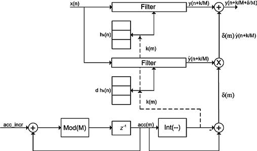
Note that the initial 1-to-4 signal up sampling can either be achieved by using two half-band filters in cascade or we can previously up sample the signals by properly choosing ![]() , the IFFT size of the synthesis channelizers. Also, at the output of the synthesizers some of the signals could be already up sampled by some factors because the IFFT size of the synthesizer has to be an even number [6] and it also has to satisfy Nyquist criteria for every signal band.
, the IFFT size of the synthesis channelizers. Also, at the output of the synthesizers some of the signals could be already up sampled by some factors because the IFFT size of the synthesizer has to be an even number [6] and it also has to satisfy Nyquist criteria for every signal band.
The arbitrary interpolator shown in Figure 7.68 performs the linear interpolation between two available adjacent signal samples (two neighbor interpolation). The interpolation process operates as follows: A new input data sample is delivered to the interpolation filter register on each accumulator overflow. The integer part of the accumulator content selects one of the M filter weights, ![]() , and one of the M derivative filter weights,
, and one of the M derivative filter weights, ![]() , while the filters compute the amplitude
, while the filters compute the amplitude ![]() and the first derivative
and the first derivative ![]() at the kth interpolated point in the M-point interpolated output grid. Then the structure uses the local Taylor series to form the interpolated sample value between grid points. The output clock directs the accumulator process to add the desired increment
at the kth interpolated point in the M-point interpolated output grid. Then the structure uses the local Taylor series to form the interpolated sample value between grid points. The output clock directs the accumulator process to add the desired increment ![]() (acc_incr in Figure 7.68) to the modulo-M accumulator and increments the output index m. The increment
(acc_incr in Figure 7.68) to the modulo-M accumulator and increments the output index m. The increment ![]() can be computed according to the following equation:
can be computed according to the following equation: ![]() . This process continues until the accumulator overflows at one of the output clock increments. Upon this overflow the input index is incremented, a new input data point is shifted into the filter, and the process continues as before.
. This process continues until the accumulator overflows at one of the output clock increments. Upon this overflow the input index is incremented, a new input data point is shifted into the filter, and the process continues as before.
1.07.9.1.3 Nyquist filters
Particular attention has to be paid in designing the low-pass prototype filters used in the analysis channelizer. The signal spectra have to be randomly located in the frequency domain and their bandwidths can easily span and occupy more than one base-line channel; also, in the signal disassembling and reassembling processes, we need to collect all the energy corresponding to a single signal without losses.
Nyquist filter presents the interesting property of having a band edge gain equal to 0.5 (or −6 dB). By using this filter as prototype in our channelizers, we place M of them across the whole spanned spectrum with each filter centered on ![]() . All adjacent filters exhibit −6 dB overlap at their band-edges. The channelizer working under this configuration is able to collect all the signal energy across its full operating spectrum range even if signals occupy more than one adjacent channel or it resides in the channel’s overlapping transition bandwidths. In the following paragraphs, for completeness, we provide a brief introduction on Nyquist filters.
. All adjacent filters exhibit −6 dB overlap at their band-edges. The channelizer working under this configuration is able to collect all the signal energy across its full operating spectrum range even if signals occupy more than one adjacent channel or it resides in the channel’s overlapping transition bandwidths. In the following paragraphs, for completeness, we provide a brief introduction on Nyquist filters.
Nyquist pulses is the name given to the wave shapes ![]() required to communicate over band-limited channels with no inter-symbol interference (ISI). When sampled at equally spaced time increments they have to verify the requirement of Eq. (7.35) which is known as Nyquist pulse criterion for zero ISI:
required to communicate over band-limited channels with no inter-symbol interference (ISI). When sampled at equally spaced time increments they have to verify the requirement of Eq. (7.35) which is known as Nyquist pulse criterion for zero ISI:
 (7.35)
There are infinite such functions that satisfy this set of restrictions. The one with minimum bandwidth is the ubiquitous ![]() which is variously known as the cardinal pulse when used for band limited interpolation and the Nyquist pulse when used in pulse shaping. The transform of this wave shape, R(f), is the unit area rectangle with spectral support 1/T Hz. Unfortunately this waveform is non-causal and further it resides on an infinite support. If the pulse resided on a finite support we could delay the response sufficiently for it to be causal. We have to form finite support approximations to the
which is variously known as the cardinal pulse when used for band limited interpolation and the Nyquist pulse when used in pulse shaping. The transform of this wave shape, R(f), is the unit area rectangle with spectral support 1/T Hz. Unfortunately this waveform is non-causal and further it resides on an infinite support. If the pulse resided on a finite support we could delay the response sufficiently for it to be causal. We have to form finite support approximations to the ![]() pulse. The first approximation to this pulse is obtained by convolving the rectangular spectrum, R(f ), with an even symmetric, continuous spectrum W(f ) with finite support
pulse. The first approximation to this pulse is obtained by convolving the rectangular spectrum, R(f ), with an even symmetric, continuous spectrum W(f ) with finite support ![]() . The convolution between R(f ) and W(f ) in the frequency domain is equivalent to a product in the time domain between the
. The convolution between R(f ) and W(f ) in the frequency domain is equivalent to a product in the time domain between the ![]() and w
and w![]() , where w
, where w![]() is the inverse transform of W(f). The effect of the spectral convolution is to increase the two-sided bandwidth from 1/T to
is the inverse transform of W(f). The effect of the spectral convolution is to increase the two-sided bandwidth from 1/T to ![]() . The excess bandwidth
. The excess bandwidth ![]() is the cost we incur to form filters on finite support. The term
is the cost we incur to form filters on finite support. The term ![]() is called the roll-off factor and is typically on the order of 0.5–0.1 with many systems using values of
is called the roll-off factor and is typically on the order of 0.5–0.1 with many systems using values of ![]() . The transition bandwidth caused by the convolution is seen to exhibit odd symmetry about the half amplitude point of the original rectangular spectrum. This is a desired consequence of requiring even symmetry for the convolving spectral mass function. When the windowed signal is sampled at the symbol rate 1/T Hz, the spectral component residing beyond the 1/T bandwidth folds about the frequency
. The transition bandwidth caused by the convolution is seen to exhibit odd symmetry about the half amplitude point of the original rectangular spectrum. This is a desired consequence of requiring even symmetry for the convolving spectral mass function. When the windowed signal is sampled at the symbol rate 1/T Hz, the spectral component residing beyond the 1/T bandwidth folds about the frequency ![]() into the original bandwidth. This folded spectral component supplies the additional amplitude required to bring the spectrum to the constant amplitude of R(f).
into the original bandwidth. This folded spectral component supplies the additional amplitude required to bring the spectrum to the constant amplitude of R(f).
Following this reasoning, we note that the significant amplitude of the windowed wave shape is confined to an interval of approximate width ![]() so that a filter with
so that a filter with ![]() spans approximately 20T, or 20 symbol durations. We can elect to simply truncate the windowed impulse response to obtain a finite support filter, and often choose the truncation points at
spans approximately 20T, or 20 symbol durations. We can elect to simply truncate the windowed impulse response to obtain a finite support filter, and often choose the truncation points at ![]() . A second window, a rectangle, performs this truncation. The result of this second windowing operation is a second spectral convolution with its transform. This second convolution induces pass-band ripple and out-of-band side-lobes in the spectrum of the finite support Nyquist filter. The description of this band-limited spectrum normalized to unity pass-band gain is presented in Eq. (7.36):
. A second window, a rectangle, performs this truncation. The result of this second windowing operation is a second spectral convolution with its transform. This second convolution induces pass-band ripple and out-of-band side-lobes in the spectrum of the finite support Nyquist filter. The description of this band-limited spectrum normalized to unity pass-band gain is presented in Eq. (7.36):
 (7.36)
The continuous time domain expression for the cosine-tapered Nyquist filter is shown in Eq. (7.37). Here we see the windowing operation of the Nyquist pulse as a product with the window that is the transform of the half-cosine spectrum:
![]() (7.37)
(7.37)
Since the Nyquist filter is band limited, we can form the samples of a digital filter by sampling the impulse response of the continuous filter. Normally this involves two operations. The first is a scaling factor applied to the impulse response by dividing by the sample rate, and the second is the sampling process in which we replace t with ![]() or
or ![]() . The sample rate must exceed the two-sided bandwidth of the filter that, due to the excess bandwidth, is wider than the symbol rate. It is standard to select the sample rate
. The sample rate must exceed the two-sided bandwidth of the filter that, due to the excess bandwidth, is wider than the symbol rate. It is standard to select the sample rate ![]() to be an integer multiple of the symbol rate
to be an integer multiple of the symbol rate ![]() so that the filter operates at M-samples per symbol. It is common to operate the filter at 4 or 8 samples per symbol.
so that the filter operates at M-samples per symbol. It is common to operate the filter at 4 or 8 samples per symbol.
In the design of the proposed analysis channelizer, the Nyquist prototype low-pass filter has to be designed with its two sided 3 dB bandwidth equal to ![]() of the channelizer input sampling frequency. This is equivalent to the filter impulse response having approximately M samples between its peak and first zero crossing and having approximately M samples between its zero crossings. The integer M is also the size of the IFFT as well as the number of channels in the analysis channelizer. The prototype filter must also exhibit reasonable transition bandwidth and sufficient out of band attenuation or stop-band level. We designed our system for a dynamic range of 80 dB which is the dynamic range of a 16-bit processor.
of the channelizer input sampling frequency. This is equivalent to the filter impulse response having approximately M samples between its peak and first zero crossing and having approximately M samples between its zero crossings. The integer M is also the size of the IFFT as well as the number of channels in the analysis channelizer. The prototype filter must also exhibit reasonable transition bandwidth and sufficient out of band attenuation or stop-band level. We designed our system for a dynamic range of 80 dB which is the dynamic range of a 16-bit processor.
1.07.9.2 Digital down converter simulation results
For simulation purposes, in this section we consider, at the input to the M-to-2 analysis channelizer, a composite spectrum that contains twelve QAM signals with five different bandwidths randomly located in the frequency domain. In particular, the signal constellations are 4-QAM, 16-QAM, 64-QAM, and 256-QAM while the signal bandwidths are 1.572132 MHz, 3.892191 MHz, 5.056941 MHz, 5.360537 MHz, and 11.11302 MHz respectively. It is clear that we used two different signal bandwidths for the 256-QAM constellation (5.360537 MHz and 11.11302 MHz).
The signals are shaped by square-root Nyquist filters with 20% excess bandwidth. At the input of the analysis channelizer all the signals are resampled for achieving 192 MHz sample rate. The spectrum is shown in Figure 7.56. In particular, the upper subplot of Figure 7.69 shows, superimposed on the composite received spectrum, the 61 channels of the analysis channelizer. It is easy to recognize that the received spectra are arbitrarily located. Their center frequencies do not coincide with the channel center frequencies. That is clearly shown in the lower subplot of Figure 7.69 in which the enlarged view of one of the received signals is presented. The arbitrary signal positioning is the reason for which the polyphase down converter channelizer, by itself, is not able to directly shift them to DC. The IFFT size of the analysis M-to-2 down converter channelizer is M = 48 with an output sample rate of 8 MHz.

Figure 7.70 shows the impulse response and the magnitude response of the designed prototype low-pass Nyquist filter. It is designed to have 48 samples per symbol. Its length is 1200 taps while its stop band attenuation is −80 dB. Note that, since this filter is M-path partitioned, the length of each filter in the M-path bank is only 25 taps.
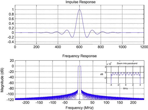
The 61 spectra, at the output of the analysis channelizer, are depicted in Figure 7.71. The down converter channelizer has partitioned the entire frequency range into 48 segments. It is easy to recognize in this figure the different spectra composing the received signal. Note that, because of the arbitrary frequency positioning, it is possible that also the signals having bandwidths narrower than the channelizer channel bandwidth occupy more than one analysis channelizer channel. Also in this case, before shifting these signals to zero frequency by using complex frequency rotators, we need to pass them through a synthesis channelizer that reassembles their fragments.

Before delivering the analysis channelizer outputs to the synthesis channelizers, we need to separate, if necessary, by filtering, those spectra that belong to different signals lying in the same channel. An example of this is represented by channel 30 in Figure 7.71. It contains fragments of two spectra belonging to different signals. The filter design in the post analysis block, of course, depends on the bands that have to be resolved. Their sample rate has to be the same as the analysis channelizer output rate (8 MHz). An example of post analysis filters along with the filtered signals, for the 30th analysis channelizer channel, is shown in Figure 7.72. In particular, the signal spectra and the filters used for separating them are shown in the upper subplot while the separated spectra are shown in the lower subplots.
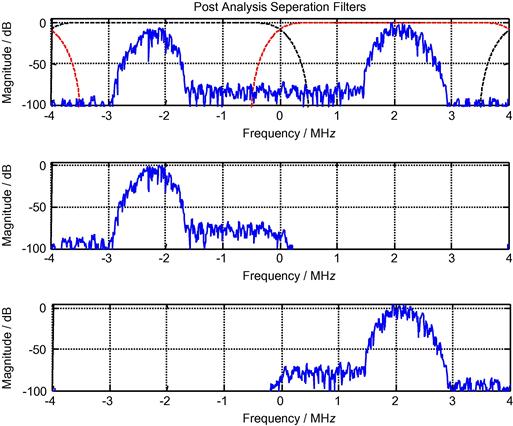
At the output of the post analysis block all the spectra, with bandwidths narrower than the analysis channel bandwidth, lying in a single analysis channel, can be directly delivered to the complex heterodyne that translates them to DC. All the other signals, the ones with bandwidths wider than the analysis channel bandwidth and, the ones with bandwidths narrower than the analysis channelizer channel bandwidth that, as consequence of the analysis process, are delivered to two different channelizer outputs, need to be processed by the small synthesis channelizers. We have, in fact, to up sample, frequency shift, and recombine the time series from coupled analysis channelizer outputs. In the example of Figure 7.69 four of the received spectra, the narrowest ones, are directly sent to the frequency rotators. Eight of them are processed through the synthesis channelizer. The IFFT sizes ![]() , with
, with ![]() of the synthesizers we selected to process the three remaining bandwidths are:
of the synthesizers we selected to process the three remaining bandwidths are: ![]() , and
, and ![]() points. These sizes are the minimum possible chosen to satisfy Nyquist sampling criterion for each output signal. Note that because of the structure of the synthesizers, we can only have an even number of IFFT points [6].
points. These sizes are the minimum possible chosen to satisfy Nyquist sampling criterion for each output signal. Note that because of the structure of the synthesizers, we can only have an even number of IFFT points [6].
At the output of the synthesizer, all the signal fragments are recombined in base-band but still some of them have a residual frequency offset that needs to be compensated. The signal spectra, before frequency offset compensation are shown in Figure 7.73. Here it is clearly visible that many of the signals are not centered at DC (the red1 line in Figure 7.73 represents the signals’ center frequency). We compensate these frequency offsets by using complex frequency rotators. Note that by estimating the signal energy in the synthesizer channels, we could easily recover the carrier offsets affecting the received spectra. The frequency offset recovery is another of the many applications of the polyphase channelizer. Other papers are being prepared for addressing this topic.

Figure 7.73 Log magnitude of synthesizer outputs with frequency offsets in the normalized frequency domain.
When they are DC centered, the signals need to be resampled. The signals at the outputs of the synthesis channelizers have different sampling frequencies. All that we need at this point is to interpolate them for obtaining exactly two samples per symbol for each of them. We use an arbitrary interpolator for achieving the sample rate conversion. The interpolated, DC shifted, signals are shown in Figure 7.74. We also match-filtered each of the eight channelized and reconstructed time signals and present their constellations in Figure 7.75, here we see that all of the QAM constellations are perfectly reconstructed which demonstrates the correct functionality of the proposed receiver.
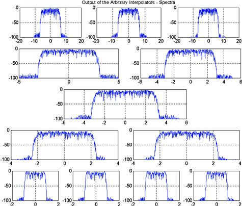

1.07.9.3 Proposed up converter architecture
Figure 7.76 shows the complete block diagram of the proposed up converter, which has the structure that is a dual of the down converter structure presented in the previous sections. It is composed of a 2-to-M up sampler synthesis channelizer, which has been presented in Section 9.5.1, preceded by N pre-processing analysis blocks which are small ![]() -to-2 analysis down converter channelizers. Their number, N, corresponds to the number of the signal spectra wider than the synthesis channelizer channel bandwidth. Their IFFT size,
-to-2 analysis down converter channelizers. Their number, N, corresponds to the number of the signal spectra wider than the synthesis channelizer channel bandwidth. Their IFFT size, ![]() , is chosen to completely span the bandwidth of the nth input signal spectrum. Their task is to decompose the wider input spectra into
, is chosen to completely span the bandwidth of the nth input signal spectrum. Their task is to decompose the wider input spectra into ![]() partitions matching the bandwidth and sample rate of the base-line synthesis channelizer which will coherently recombine them in the receiver.
partitions matching the bandwidth and sample rate of the base-line synthesis channelizer which will coherently recombine them in the receiver.
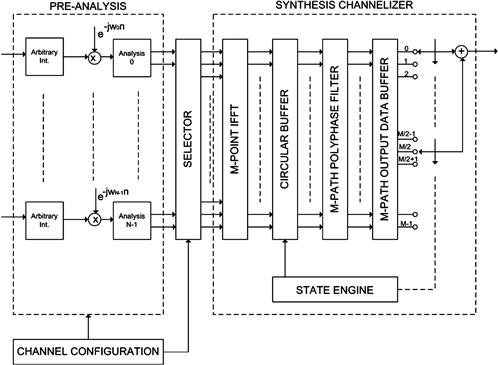
Figure 7.76 Block diagram of the proposed up converter; arbitrary interpolators, complex frequency rotators, analysis down converter channelizers and synthesis up converter channelizer.
All the input signals to the 2-to-M synthesis channelizer with bandwidths less than or equal to the channel spacing are to be up sampled and translated from base-band to the selected center frequency by the channelizing process. For these signals we may only have to filter and resample to obtain the desired sampling rate of two samples per channel bandwidth. However, we expect that many of the spectra we presented to the synthesis channelizer have bandwidths that are wider than the synthesizer channel spacing. For accommodating these signals we need to use the small analysis channelizers that partition their bandwidths into several fragments, translate all of them to base-band, and reduce their sample rate to twice the channel bandwidth. The analysis channelizers are designed as ![]() -to-2 polyphase down converter channelizers where
-to-2 polyphase down converter channelizers where ![]() is approximately twice the number of base-line channels spanned by the wideband spectrum. They have been presented in Section 1.07.5 of this same document and Figure 7.55 shows their block diagram.
is approximately twice the number of base-line channels spanned by the wideband spectrum. They have been presented in Section 1.07.5 of this same document and Figure 7.55 shows their block diagram.
We briefly recall here that such a system accepts N/2 input samples and outputs time samples from N output channels. The N-point input buffer is fed by a dual input commutator with an N/2 sample offset. The N-path filter contains polynomials of the form ![]() and
and ![]() in its upper and lower halves respectively. The circular output buffer performs the phase rotation alignment of the IFFT block with the N/2 stride shifting time origin of the N-path polyphase filter. The IFFT size for these analysis channelizers,
in its upper and lower halves respectively. The circular output buffer performs the phase rotation alignment of the IFFT block with the N/2 stride shifting time origin of the N-path polyphase filter. The IFFT size for these analysis channelizers, ![]() , is also the number of their filter outputs.
, is also the number of their filter outputs.
In order to recombine the segmented signal components we have to satisfy the Nyquist criteria for their sum. Since these are pre-processor analysis channelizers that feed the M-path synthesis channelizer we must have their output sample rate two times their channel bandwidth. We can achieve this by selecting ![]() to be approximately twice the number of channels being merged in the synthesizer and setting its input sample rate to be
to be approximately twice the number of channels being merged in the synthesizer and setting its input sample rate to be ![]() so that the pre-processor output rate per channel is the required
so that the pre-processor output rate per channel is the required ![]() . Remember that the IFFT block sizes must be even to perform the 2-to-N resampling by the technique described in Section 1.07.5; also remember that, an actual system may have a few standard size IFFT’s to be used for the analysis channelizer and the user may have to choose from the small list of available block sizes.
. Remember that the IFFT block sizes must be even to perform the 2-to-N resampling by the technique described in Section 1.07.5; also remember that, an actual system may have a few standard size IFFT’s to be used for the analysis channelizer and the user may have to choose from the small list of available block sizes.
The channel selector placed between the analysis channelizer bank and the synthesis channelizer also connected with the input channel configuration block provides the correct outputs from the pre-processor analysis channelizer to the input synthesizer while the channel configuration block provides the necessary information to the selector block that is connected to the synthesis input series. The selector routes all the segments required to assemble the wider bandwidth channel to the synthesizer which performs their frequency shift and reassembly.
Depending on the desired center frequency of the disassembled spectrum an earlier complex heterodyne may be required before the analyzers to shift of the about to be disassembled signals with the proper frequency offset.
1.07.9.4 Digital up converter simulation results
In the simulation results shown in this section we consider a set of eight distinct base-band input signals to be delivered to the 2-to-M up converter synthesis channelizer. These are QPSK signals with three different bandwidths as shown in Figure 7.77. The symbol rates chosen for the three signals denoted 1, 2, and 3, are 7.5, 15.0, and 30.0 MHz. These signals are shaped by square-root Nyquist filters with 25% excess bandwidth, hence the two sided bandwidths are 7.5![]() 1.25, 15.0
1.25, 15.0![]() 1.25, and 30.0
1.25, and 30.0![]() 1.25 MHz respectively.
1.25 MHz respectively.
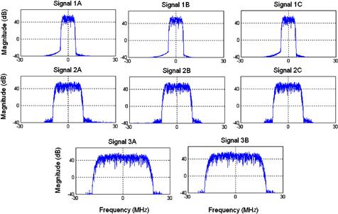
The IFFT size of the base-line 2-to-M up converter channelizer is M = 48 with 10 MHz channel spacing for which the required input sample rate per input signal is 20 MHz and for which the output sample rate will be 480 MHz. For ease of signal generation, all three signals were shaped and up-sampled to 60 MHz sample rate with shaping filters designed for 8, 4, and 2 samples per symbol. Signal 1, represented in the first line of Figure 7.77, is down sampled 3-to-1 to obtain the desired 20 MHz sample rate for the synthesis channelizer. Signals 2 and 3, respectively on the second and third line of Figure 7.77, are down sampled 6-to-2 in the six point IFFT analysis channelizers which form 10 MHz channels at 20 MHz sample rate. Signal 2 is spanned by three 10 MHz channels which will feed 3 input ports of the 48 point synthesizer IFFT while signal 3 is spanned by five 10 MHz channels which will feed 5 input ports of the 48 point IFFT. The IFFT inputs are controlled by a channel control block that routes them to the proper synthesis channelizer ports.
Any of the signals presented to the analysis channelizers is previously shifted to a desired frequency offset, by means of a complex heterodyne if required. The output channels that span the offset input bandwidth of the analysis channelizer are the channels passed on the synthesizer and these change due to a frequency offset. The inserted base-band frequency offset will survive the synthesis channelizer.
Figure 7.78 shows all the spectra of the output time series from the 6-channel polyphase 6-to-2 analysis channelizer engine processing signal 3 which is the signal with the widest band. Also seen, in the same figure, is the spectrum of signal 3 and the frequency response of all the 6 channels formed by one of the analysis channelizers. Note the spectra in the upper subplots have been filtered by the channelizer with the 10 MHz Nyquist pass band frequency response, have been translated to base-band and have been sampled at 20 MHz. Five of these segments are presented to the five input ports of the 2-to-48 synthesis channelizer centered on the desired frequency translation index.
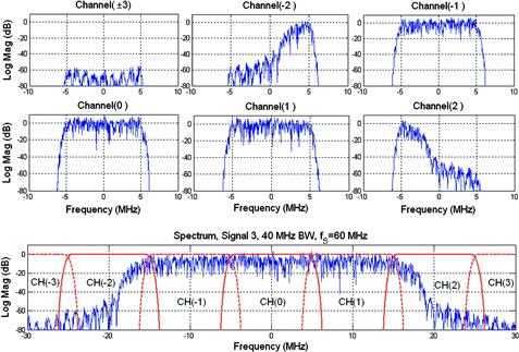
Figure 7.78 Spectral fragments formed by 6-channel 6-to-2 down sample analysis channelizer processing signal 3.
The up converter polyphase synthesis channelizer accepts time sequences sampled at 20 MHz with bandwidths less than 10 MHz. We have delivered three signals that satisfy these constraints along with four signals that were conditioned by analysis channelizers that partitioned their bandwidths into segments that also satisfied the input signal constraints. The spectra of the separate components delivered to the synthesis channelizer are shown in Figure 7.79. It is easy to recognize in this figure the different spectra composing the received signal. Here we see that filters 4-through-8 are segments of a single frequency band fragmented in Figure 7.78.
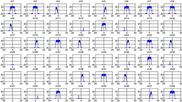
At this point, we up sample, frequency shift, and recombine the time series from coupled channel outputs using the synthesis channelizer. The frequency shifted spectra of the eight signals, including six that have been fragmented in analysis channelizers and then defragmented in the synthesis channelizer are plotted in Figure 7.80.

1.07.10 Closing comments
This chapter had the intention of providing the basic concepts on multirate signal processing and polyphase filter banks to which, when an IDFT block and a commutator are applied, are known as polyphase channelizer because of the processing task that they perform on the input signals. This chapter also had the intention of presenting innovative results on software and cognitive radio designs. While the polyphase filter banks and polyphase channelizers are well known topics in the DSP area, the software radio design is still an open research topic.
The document started with preliminaries, in Section 1.07.2, on the resampling process of a digital signal as opposed to the sampling process of an analog signal. In Section 1.07.3 an introduction on digital filters has been provided and the differences with the analog filters have been explained. In Section 1.07.4 an introduction on the window method for digital filter design has been provided. Multirate filters have been defined and explained in Section 1.07.5 while the polyphase decomposition of a prototype filter has been introduced in Section 1.07.6 along with the standard up sampler and down sampler polyphase channelizers. In Section 1.07.7 the modifications of the standard polyphase channelizer that allow us to change the output sampling rate have been presented. These engines are the basic components of the proposed architectures (presented in Sections 1.07.8 and 1.07.9): the synthesis and analysis channelizers, that are suitable for being used as software defined transmitter and receiver respectively.
The synthesis channelizer, in fact, when supported by small analysis channelizers, is able to simultaneously up convert multiple signals having arbitrary bandwidths to randomly located center frequencies. In this engine small analysis channelizers pre-process wider bandwidth signals into segments acceptable to the following synthesis channelizer that up samples, translates to the proper center frequency, and reassembles them. A channel selector block, connected with a channel configuration block, is used to properly deliver the analysis channelizer outputs to the synthesis channelizer.
On the other side of the communication chain, the analysis channelizer, that is thought for being embedded in a SDR receiver, when supported by small synthesis channelizers, is able to simultaneously demodulate these signals. A channel configuration block, inserted in the receiver, communicates with a selector block that properly delivers the analysis channelizer outputs to the synthesizer up converters that follow it. These synthesizers up sample, translate and reassemble the spectral fragments when they belong to the same source signal. Nyquist prototype low-pass filters, which are perfect reconstruction filters, are used to allow the reconstruction of the signal fragments without energy losses.
Complex frequency rotators are used for compensating residual frequency offsets and arbitrary interpolators provide us exactly two samples per symbol required for the following processing tasks of the receiver.
Theoretical reasoning and simulation results are presented, for both the receiver and the transmitter, in order to demonstrate their correct functionality.
Note that because in both of the proposed DUC and DDC structures, the IFFT sizes of the small synthesis and analysis channelizers are chosen in order to give us at least two samples per symbol for every processed bandwidth, they result to be very efficient, from a computational point of view, when the received signal is composed of spectra with widely varying bandwidths.
Slightly different versions of channelizers can be used based on different input signals and/or for adding functionalities to the proposed architectures. Channelizers are, in fact, highly efficient and very flexible structures. Among their most common applications we find spectral analysis, modem synchronization (phase, frequency and time) and channel equalization.
Glossary
Filter calculation procedure that transforms the input signals into others
Digital filter filter that operates on digital signals
Multirate filter digital filter that contains a mechanism to increase or decrease the sampling rate while processing input signals
Polyphase filter digital filter partitioned by following Eq. (7.3)
Polyphase channelizer flexible digital device which can arbitrarily change the sample rate and the bandwidth of the input signal and can also select randomly located Nyquist zones
Software radio radio device in which the digitization of the signal occurs before the intermediate frequency translation
Cognitive radio software radio with the capability to adapt its operating parameters according to the interactions with the surrounding radio environment
References
1. Kranc George M. Input-output analysis of multirate feedback systems. IRE Trans Automat Control AC-2 1956;21–28.
2. Jury EI, Mullin FJ. The analysis of sampled-data control systems with a periodically time-varying sampling rate. IRE Trans Automat Control-4 1959;15–20.
3. Jury EJ, Mullin FJ. The analysis of sampled data control system with a periodically time varying sampling rate. IRE Trans Automat Control AC-4 1959;15–21.
4. Vary P, Heute U. A short-time spectrum analyzer with polyphase-network and DFT. Signal Process. 1980;2(1):55–65.
5. Schafer RW, Rabiner LR. Design of digital filter banks for speech analysis. Bell Syst Tech J. 1971;50:3097–3115.
6. Harris FJ. Multirate Signal Processing for Communication systems. New Jersey: Prentice Hall, Upper Saddle River; 2004.
7. Harris F, Lowdermilk W. Software defined radio. IEEE Instrum Meas Mag 2010.
8. Harris F, Dick C, Chen X, Venosa E. Wideband 160 channel polyphase filter bank cable TV channelizer. IET Signal Process. 2010.
9. F. Harris, C. Dick, X. Chen, E. Venosa, M-path channelizer with arbitrary center frequency assignments, in: WPMC 2010, March 2010.
10. X. Chen, E. Venosa, F. Harris, Polyphase synthesis filter bank up-converts unequal channel bandwidths with arbitrary center frequencies-design II, in: SDR 2010, Washington, DC, December 2010.
11. E. Venosa, X. Chen, F. Harris, Polyphase analysis filter bank down-converts unequal channel bandwidths with arbitrary center frequencies-design II, in: SDR 2010, Washington, DC, December 2010.
12. Bellanger M, Bonnerot G, Coudreuse M. Digital filtering by polyphase network: application to sample-rate alteration and filter bank. IEEE Trans Acoust Speech Signal Process. 1976;24(2):109–114.
13. Bellanger M, Daguet J. TDM-FDM transmultiplexer: digital polyphase and FFT. IEEE Trans Commun. 1974;22(9):1199–1205.
14. Ribey M. Exploration of transmultiplexers in telecommunication networks. IEEE Trans Commun COM-30 1982;1493–1497.
15. Wang B, Ray Liu KJ. Advances in cognitive radio networks: a survey. IEEE J Sel Top Signal Process. 2011;5.
16. Sahai A, Mishra SM, Tandra R, Woyach KA. Cognitive radios for spectrum sharing. IEEE Signal Process Mag. 2009;26.
17. Sherman Matthew, Rodriguez Christian, Reddy Ranga. IEEE standards supporting cognitive radio and networks, dynamic spectrum access, and coexistence. IEEE Commun Mag. 2008;46.
18. Ma Jun, Ye Li G, Juang Biing Hwang (Fred). Signal processing in cognitive radio. Proc IEEE. 2009;97.
19. Ulversøy T. Software defined radio: challenges and opportunities. IEEE Commun Surv. 2010;2.
20. Bagheri R, Mirzaei A, Heidari ME. Software-defined radio receiver: dream to reality. IEEE Commun Mag. 2006;44.
21. Mitola J. Cognitive radio architecture evolution. Proc IEEE. 2009;97.
22. Tandra R, Mishra SM, Sahai A. What is a spectrum hole and what does it take to recognize one? Proc IEEE. 2009;97.
23. Fredric J. Harris, On detecting white space spectra for spectral scavenging in cognitive radios, Springer J. Wireless Pers. Commun. <http://dx.doi.org/10.1007/s11277-008-9460-y>.
24. Harris F, Dick C, Rice M. Digital receivers and transmitters using polyphase filter banks for wireless communications. Microwave Theory Tech. 2003;51(4):1395–1412 (special issue).
1For interpretation of color in Figure 7.73, the reader is referred to the web version of this book.