
5
Integrated Optics
5.1 Planar Optical Waveguide Theory
We first discuss the case of the planar waveguide in terms of the carrier compensation process. If the waveguide core layer is assumed homogeneous, then the amount of free-carrier compensation necessary for waveguiding, that is, at least for the fundamental transverse electric mode (TE0) to propagate, can be calculated. This cutoff condition for TE0 to propagate is [1]
Since n2 ≫ n3 and n1 ≥ n2, the argument of the inverse tangent is much greater than unity but is not always large enough in the cases considered for arctan(x) to be approximated by π/2. Therefore, the simple mathematical identify arctan(x) = π/2—arctan(1/x) allows an accurate Taylor series approximation to be made. Note that
and that
results in the following condition, which is the minimum index change necessary for waveguiding:
Expressing Δn in terms of the free-carrier concentrations in both the core and substrate regions gives the carrier compensation necessary for waveguiding to occur:
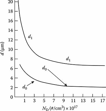
FIGURE 5.1
Cutoff thickness versus substrate doping for λ0 = 1.3 μm.
In general, the carrier compensation necessary for guiding the TE1 (1-th order) mode is given by the expression
Figures 5.1 through 5.3 illustrate representative cutoff thickness versus substrate doping curves for three wavelengths of interest. The assumption is made that essentially complete carrier compensation will occur in the waveguide fabrication process.
5.2 Comparison of “Exact” and Numerical Channel Waveguide Theories
A number of workers have analyzed lossless dielectric waveguide structures including Marcatili, Goell, Schlosser, Bartling, and Shaw [2]. Goell represented the radial variation of the longitudinal electric and magnetic fields of the circular dielectric waveguide modes by a sum of modified Bessel functions inside and outside the waveguide core. Matching the fields along the perimeter of the core provided computer solutions. Schlosser’s analysis was for the case of a dielectric rod in air and applied to index of refraction differences more applicable to microwaves. Bartling solved the problem in terms of a Green’s dyadic but did not calculate specific cases.
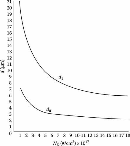
FIGURE 5.2
Cutoff thickness versus substrate doping for λ0 = 3.4 μm.
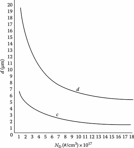
FIGURE 5.3
Cutoff thickness versus substrate doping for λ0 = 10 μm.
After some simplifying assumptions, Marcatili solved Maxwell’s equations in closed form for rectangular cross section dielectric waveguides of various aspect ratios. Proper selection of the index of refraction results in a waveguide supporting only the fundamental modes in a family of two types of hybrid transverse electric magnetic (TEM) modes polarized at right angles.
Marcatili’s analysis provides analytical results in a relatively simple form and is preferred since the calculations required are simpler. Goell suggests that the analysis may not provide the accuracy desired for the lowest order mode, however [3], as shown in Figure 5.4. Figure 5.4 provides solutions from Marcatili’s transcendental and closed form equations and Goell’s circular harmonic solutions for an aspect ratio (channel width to height ratio) of 2, with an index difference in the channel greater than 1.05 times that of the surrounding dielectric. The two methods indicate values of a normalized propagation constant (in terms of the transverse and waveguide propagation constants)
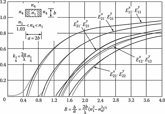
FIGURE 5.4
Propagation constant for several modes of rectangular dielectric waveguide. Transcendental solution …… ; closed form solutions __; Goell’s computer solution.
which are within a few percent for p2 > 0.5, although Goell indicates a “fanning out” to the left on the curves for small p2.
An analysis performed by Bradley and Kellner [4] was used to verify the accuracy of Marcatili’s approach as applied to carrier compensated waveguides. The numerical analysis program uses cubic spline functions in a finite element analysis. The comparison indicates essentially perfect agreement with the modal structure and cutoff conditions predicted by the Marcatili analysis (excepting very small p2 values), so that the ease afforded by the use of Marcatili’s approach does not significantly compromise the accuracy or choice of fabrication parameters.
5.3 Modes of the Channel Waveguide
The basic channel structure is shown in Figure 5.5. In many cases of interest, n3 = n4 = n5 < n1 and n2 = n1; however, the more general case will be discussed first. A simplification at this point enables a closed form solution. The key assumption is that the modes are well above cutoff, so that the field decays exponentially in regions 2, 3, 4, and 5, with most of the power traveling in region 1. Very little power travels in the shaded regions of Figure 5.5 so that, by not matching the fields along the edges of the shaded areas, we are not significantly affecting the calculation of fields in region 1.
The modes are essentially of the TEM type and can be grouped into two families, modes, Ex and , with p and q indicating the number of extrema in the field distributions in the x- and y-directions, respectively. The transverse field components of the modes, Ex modes are Ex and Hy, while those of the modes are Ey and Hx. Figure 5.6 shows the fundamental mode E11, characterized by extinction coefficients n2, e3, n4, and e5 in the regions where the mode is exponential, and by propagation constants kx and ky in region 1. In cases where n3 = n5, the fields will be symmetric with respect to the x = 0 plane.
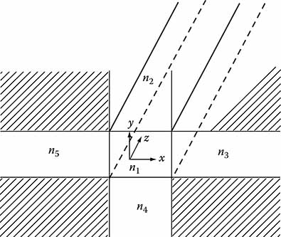
FIGURE 5.5
Ion-implanted channel waveguide structure.
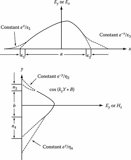
FIGURE 5.6
Field distribution of the fundamental mode11 for a guide immersed in several dielectrics.
Quantitative expressions for kx, ky, n, and e are now determined.
Assuming that the plane wavelets that make a mode impinge on the interfaces at grazing angles, that is, 1/n1(n1 − ny) ≪ 1, then k, , and are given by
The modes are polarized such that Ey is the only significant component of electric field with Ex and Ez negligibly small. In the case of the modes, Ex is the only significant electric field component.
A computer code was written to calculate the modes of channel waveguides using Marcatili’s equations. The program provides the e’s, n’s, and neff’s = kz’s for any particular channel guide design. The goal of the design process was to determine the fabrication parameters that would produce a guide with the least amount of propagation loss possible and with only single mode propagation. The key factor in the determination of these optimum parameters is the minimization of the optical power guided in the mode tails residing in the substrate, that is, n3, n4, n5 region. Calculations of waveguide cutoff curves and losses for any aspect ratio can be performed for any propagation wavelength. Figures 5.7 through 5.9 are the propagation cutoff curves at 1.3, 3.4, and 10.6 μm wavelengths for an aspect ratio of 1. These curves, along with the accompanying loss versus ND curves, provide the basis for the selection of ND, t, and aspect ratio at each wavelength for channel waveguides. In addition, Figures 5.10 through 5.12 indicate the specific range or distance on the cutoff curve x-axis, over which the and modes are guided but the and modes are not guided, versus ND and aspect ratio. This thickness tolerance is important since it decreases, for example, with increasing aspect ratio. Since a thickness is generally chosen somewhere near the center of this range to prevent any fabrication error causing either multimode or no mode guiding, this range is an important design consideration.
5.4 Directional Couplers
The dual channel directional coupler consists of parallel channel waveguides spaced so that synchronous coherent coupling between the overlapping evanescent mode tails occurs. Figure 5.13 illustrates such a device. The electrical properties and field penetrations e35 and n24 for the parallel guides shown in Figure 5.13 are the same as those of the isolated channel. Such a parallel channel directional coupler can transmit both the and modes.
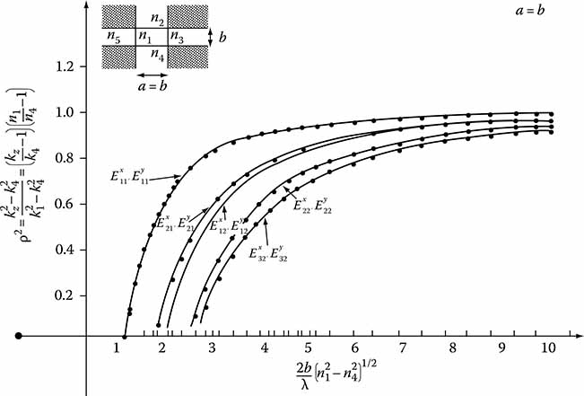
FIGURE 5.7
Propagation cutoff curve for λ0 = 1.3 μm.
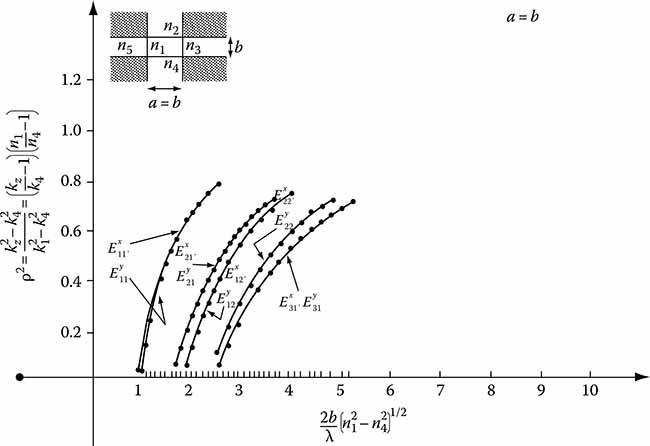
FIGURE 5.8
Propagation cutoff curve for λ0 = 3.4 μm.
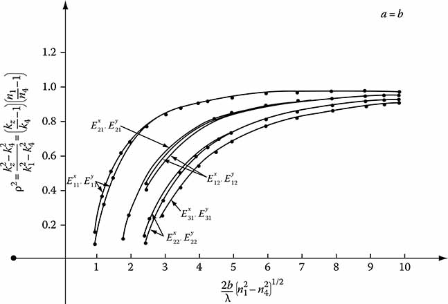
FIGURE 5.9
Propagation cutoff curve for λ = 10.6 μm.
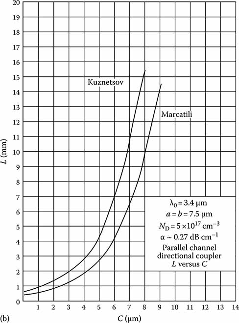
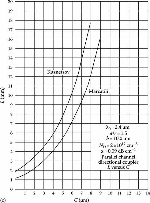
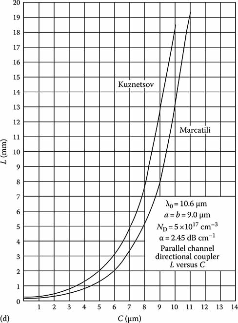
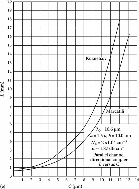
Following the analysis of Marcatili [5], the coupling coefficient K between the two guides and the length L (along the z-direction) necessary for complete transfer of power from one to the other is given by
A more-accurate expression for the coupling was published by Kuznetsov [6]. This work indicated that the Marcatili analysis overestimates the coupling coefficient, especially in the weaker-guiding cases, by as much as a factor of 2. The design program used for channel guides was also written to calculate the coupling length L for any separation C, for identical guides, for the X-polarized electrical field. Both the Marcatili and the Kuznetsov values of coupling length have been determined as a direct basis for comparison.
Following are plots of the predicted coupling lengths versus channel separations for several representative channel waveguide designs (Figure 5.14a through e). Accurate control of the guide separation is very important since the coupling length L decreases exponentially with the ratio c/e5, where e5 is the transverse mode extinction coefficient. In fact, for separations C < e5 there will be a significant perturbation upon the optical mode field profile by each channel upon the other. Predictions of the coupling length for separations less than e5, therefore, would require a more extensive analysis of the perturbation effect.
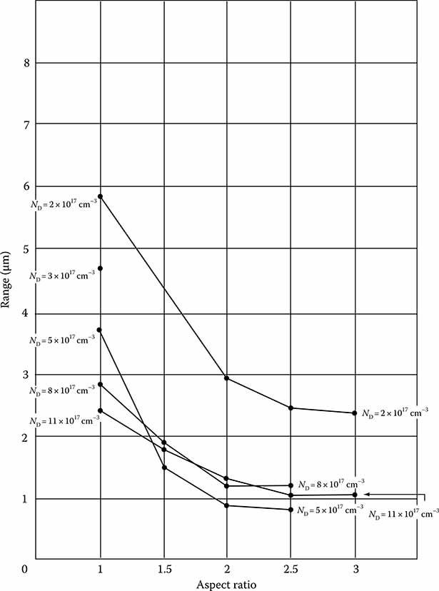
FIGURE 5.10
λ0 = 1.3 μm—Maximum range of thickness for guiding only the models.
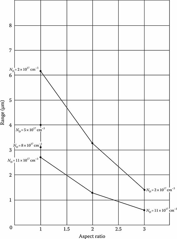
FIGURE 5.11
λ0 = 3.4 μm—Maximum range of thickness for guiding only the modes.
5.5 Key Considerations in the Specifications of an Optical Circuit
5.5.1 Introduction
A number of key interrelated issues need to be addressed in order to properly specify an integrated optical circuit. These considerations include operational wavelength, optical throughput losses, material growth, electronic and microwave compatibility, and integratability. Much of the work in the field of optical circuit engineering has involved optimization of a particular performance aspect. The next step is to realize fully optimized integrated optical circuit systems.
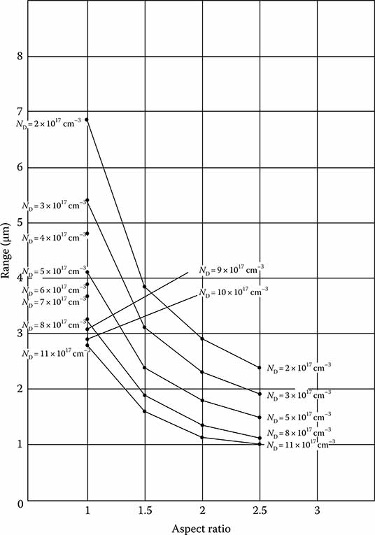
FIGURE 5.12
λ0 = 10.6 μm—Maximum range of thickness for guiding only the modes.
Of all the considerations involved in the selection of substrate material, optical loss is often the overriding factor. Optical loss is generally due to artifacts of fabrication such as surface roughness, interface strain and defects, nonideal or non-abrupt dielectric discontinuity, and unwanted interstitial defect trapping and scattering centers. Aside from optical absorption occurring via free-carrier absorption of power residing in heavily doped regions of the optical mode profile, it is the interband or band-edge absorption which will dominate the optical power budget. Purity and control of the fabrication environment provide both low-loss material (e.g., minimize unwanted tailing of the absorption band edge), and optimum surface and interference quality for both efficient electro-optic interaction and maximum optical throughput.
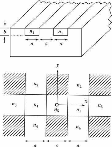
FIGURE 5.13
Parallel channel directional coupler.
Intrinsic semiconductor loss is primarily due to free-carrier absorption, so that selection of the 0.86 μm wavelength is not a disadvantage in terms of loss relative to 1.3 μm provided the band edge of the optical waveguide relative to the light source is properly chosen. Losses due to interband absorption are a serious consideration at 0.86 μm, but with enhanced material growth and fabrication capability, considerably improved quality materials (i.e., vastly improved control of defect concentration) will be more readily available.
The larger amount of waveguiding loss at 0.86 μm can be compensated for by several approaches. First, at 0.86 a GaAlAs laser diode can be integrated with other optical components on the same chip to reduce coupling loss. The required technology to do this at 1.3 μm is considerably lacking. Fabrication of microwave transistor monolithic integrated circuits and digital integrated circuits is much farther advanced for GaAs compared to InP. This alone might suggest the choice of GaAs as a substrate material. Optical amplifiers at 0.86 μm can be built with better than 20 dB gain [7]; therefore in terms of system loss, the addition of this one additional component on the chip is advantageous. Furthermore, since the structure required for the optical amplifier is identical to the laser diode structure, the fabrication complexity will not be significantly increased.
Numerous current and downstream applications for 0.86 μm integrated optics technology provide substantial justification for its continued development. A powerful motivation for working in the 0.86 μm region is the blossoming area of nonlinear optics, or exitonic absorption phenomena, which are expected to permit the realization of modulation and switching speeds on the order of 100 fs (10−13 s). Optical systems with this capability will find application in optical signal processing for digital computation and for total information wide-band processing as required in the multi-information coded channel scenario of the modern battlefield, and in the complexity of the international and satellite audio and visual communications [8]. These structures are extremely important from the stand point of basic science because their submicron geometry necessitates altering the traditional, mathematical, and physical analysis.
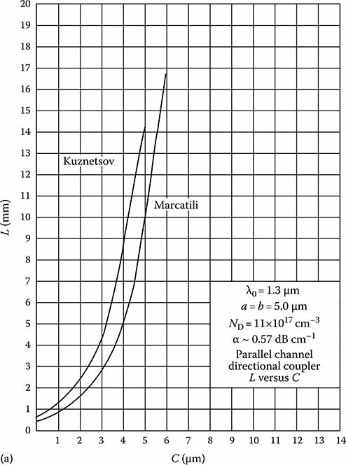
FIGURE 5.14
(a) λ0 = 1.3 μm; a = b = 5.0 μm; ND = 11 × 1017 cm−3 parallel direction channel directional coupler L versus C. (b) λ0 = 3.4 μm; a = b = 7.5 μm; ND = 5 × 1017 cm−3; α ∼ 0.27 db cm−1 parallel direction channel directional coupler L versus C. (c) λ0 = 1.3 μm; a/r = 1.5; b = 10.0 μm; ND = 2 × 1017 cm−3; α = 0.09 db cm−1 parallel direction channel directional coupler L versus C. (d) λ0 = 10.6 μm; a = b = 9.0 μm; ND = 5 × 1017 cm−3; α = 2.45 db cm−1 parallel direction channel directional coupler L versus C. (e) λ0 = 10.6 μm; a = 1.5b; b = 10.0 μm; ND = 2 × 1017 cm−3; α ∼ 1.87 db cm−1 parallel direction channel directional coupler L versus C.
The material quality and critical fabrication tolerances afforded through MOCVD and the MBE permit fabrication of single crystals with nanometer dimensions and ultimately single monatomic layers. This gives rise to previously unexplored conditions such as ellipsoidal symmetry of the exciton and layer thicknesses less than the mean free path of the electron, and hence effects such as exciton stability at room temperature and ballistic tunneling of electrons and hot electrons. These effects will ultimately be implemented in a guided-wave integrated format, affording improved optical system performance.
5.5.2 Waveguide Building Block and Wavelength Selection
Various fundamental waveguide structures have been investigated for use with GaAs substrates (LiNbO and other material systems will be discussed in a later section). These structures will be reviewed in this section along with the factors leading to the final preferred choice. Several structures are made without the use of multiple materials. Ion implantation has been shown to produce the necessary change in the refractive index of the substrate material to induce waveguiding [9]; however, free-carrier absorption loss due to the heavily doped substrates results in losses on the order of 1 dB cm−1 [10].
Another alternative is the use of deposited/etched thin-film dielectric waveguides [11] on the surface of the GaAs wafer. This is a fairly attractive option because a waveguide material such as SiO2 or Ta2O2 would not exhibit either interband absorption or free-carrier absorption. It might, therefore, be possible to obtain less than 1.0 dB cm−1 loss over the entire wavelength range of 0.82–1.3 μm; however it is very difficult to couple light from a device such as a laser or modulator in the GaAs wafer into the waveguide without considerable coupling loss because the index of refraction of GaAs is so much larger than that of the dielectric. The three exposed surfaces of the dielectric waveguide are also subject to damage and degradation due to physical abrasion and atmospheric contaminants. To act as a waveguiding region the deposited film would need to be isolated from the GaAs substrate by another film having a lower refractive index than the waveguiding film. In the past it has been difficult to deposit such a two-layer structure and achieve low waveguiding loss. There is also the possibility of the waveguide lifting from the GaAs surface because of mismatch in the thermal expansion coefficients.
Other structures can be formed by growing epitaxial AlGaAs layers on the substrate. These layers yield a planar waveguide, providing mode confinement in the vertical direction. Some form of etching or ion milling is then used to define a structure that also provides confinement in the lateral direction. Three such structures are the raised rib, the buried encapsulated, and the buried strip-loaded waveguides. Schematic diagrams of these structures are shown in Figure 5.15.
The first two structures have some obvious disadvantages. The raised rib design has most of the confined mode present in the rib. This is subject to a great deal of scattering loss from the etched side walls of the guide. Because the guide is on the surface, it is also subject to damage and contamination. The encapsulated design avoids this second pitfall but relies on more complicated lithographic techniques and material growth. This latter aspect presents significant difficulty when considering electronic and full optical integration in conjunction with the waveguides.
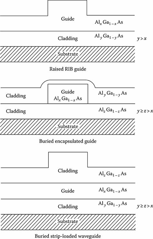
FIGURE 5.15
Fundamental AlGaAs waveguides.
For the above reasons the buried strip-loaded structure may be the optimum approach. This structure has better vertical confinement which keeps the guided energy away from the surface and minimizes scattering losses. The fact that the etched boundaries are located within the cladding layer also reduces their effect on scattering losses, particularly in comparison to the raised rib guide. The additional layering provides for the incorporation of fabrication features such as a stop etch layer. In addition this structure gives better p–n junction characteristics when an electro-optic modulator is being fabricated and provides greater design freedom for the problem of contacting. One detrimental feature of this structure is that it has less lateral confinement, making it more lossy for waveguide bends if not very carefully designed. Numerical examples in another section illustrate this point.
The fundamental constraint on the operational wavelength of this waveguide is normally that the light be confined in a single mode. With a GaAs substrate, the clear choice for the waveguide structure is the AlGaAs/GaAs system. The AlGaAs system will guide light over a range of wavelengths from less than 0.8 μm to greater than 10.6 μm. For AlGaAs waveguides, the wavelengths that have received the most attention are 0.85 and 1.3 μm. Since wavelengths longer than about 0.87 μm are not possible with an integrated source in the AlGaAs material, the final constraint becomes the wavelength of the source. If operation speed is to be in excess of 3 Gb s−1, performance can be improved by integrating the lasers and electronic drive circuitry with the rest of the optical components.
The one performance parameter that probably will not exceed that which can be done at 1.3 μm is optical waveguide loss. Losses in AlGaAs waveguides are typically 1 dB cm−1 while losses at 0.85 μm are often 2–4 dB cm−1 due to band-edge material loss. As available material quality improves the optical losses will improve. One must consider not only waveguide absorption and scattering loss but also laser to waveguide coupling loss and the advantages to be gained from monolithic integration. Without anti-reflection coating applied to the facets of the waveguide, it is difficult to achieve better than 50% coupling efficiency into an AlGaAs waveguide since reflection loss itself is 30%. End fire or butt coupling losses will be dramatically reduced when the laser is integrated on the substrate. The AlGaAs multilayer material system is much more developed than the InGaAaP so that one would expect lower values of waveguide loss with the former when lasers are monolithically integrated. Although use of the InGaAsP lasers at 1.3 μm wavelength as sources for waveguides formed in AlGaAs can achieve lower values of loss, one gives up the potential for monolithic integration of lasers with integrated optical devices. Another method that can be used to compensate for optical loss is to integrate an optical amplifier on the substrate. Optical amplifiers exhibited gains in excess of 20 dB [12]. Although this demonstration was at a wavelength of 1.5 μm, it could also be achieved in AlGaAs waveguides at 0.85 μm.
The 1.3 μm lasers consist of InGaAsP layers grown on InP substrates. This wavelength is a good choice for specialized long haul communications (distances longer than 10 km); however, because GaAs is transparent at this wavelength, the fabrication of lasers and detectors on the same substrate with GaAs electronics would be extremely difficult. In addition, there is a large lattice mismatch between InP and GaAs.
Higher reliability is achieved by reducing the number of components via larger scale integration. Since sources and detectors can be readily integrated on GaAs substrates the number of hybrid components can be reduced. The least reliable part of any electronic or optoelectronic package is often the wire bonds. With a single monolithic integrated optic/optoelectronic chip the number of wire bonds decreases and reliability improves. This can also be translated to lower cost since the entire process will be subjected to well-calibrated batch fabrication processes.
An additional advantage of increased flexibility exists at the 0.85 μm wavelength. There are large research and development efforts in fabricating optical logic devices using AlGaAs/GaAs multiple quantum well structures. These devices rely on a resonant excitonic absorption and must be operated near the material band edge. This means that the wavelength must be in the 0.8–0.9 μm range (depending on Al concentration). These devices have shown the capability to operate at more than 10 GHz [13] with energies of less than 5 pJ [14]. Several logic gates have been demonstrated including XOR, NOR, and OR [15]. The capability of incorporating optical logic in a system can significantly improve the flexibility of the entire system.
Smearing of quantum wells of AlGaAs by diffusion of Zn or implantation of Si has been demonstrated and is under investigation in several laboratories. As the refractive index of the AlGaAs alloy is different than that of the original multi quantum well structure this effect provides an additional parameter that can be used for optical confinement, particularly in the lateral direction.
5.5.3 Optical Throughput Loss
Many forms of loss encountered in the waveguide can be related to a number of factors. These are material properties which include growth effects, the processing of the material for waveguide fabrication, and simply the design requirements. A reasonable fabrication but fairly stringent design tolerance for a GaAs/GaAlAs waveguide system might be 1 dB cm−1 loss in straight sections for the waveguide and 0.3 dB rad−1 loss in curved sections of the waveguide. This requires careful design and fabrication to minimize all contributors to loss, that is, interband absorption, free-carrier absorption, scattering, and radiation.
The major loss to be dealt with in an AlGaAs system is band-edge or interband absorption. In an ideal system, this loss can be overcome by simply using a waveguide of slightly less energy than the bandgap of the waveguide material less the energy of acceptors. In a real material with a source wavelength close to the band edge, a certain amount of loss is unavoidable due to deep level states. A large part of this loss can be attributed to band-edge tailing resulting from various defects and impurity states in the material. The quality of the material used for the waveguide can thus be directly correlated with the loss.
Using the early absorption data of Sturge [16] and Stoll et al. [17], one would project that interband absorption loss would be greater than 1 dB cm−1 for wavelengths shorter than 0.92 μm in waveguides with an aluminum concentration of 40%. More recent studies have measured losses of 3–5 dB cm−1 at wavelengths of 0.86 μm. The high quality material now available will further reduce losses to an acceptable level. It is actually inadvisable to reduce losses by going to aluminum concentration greater than 20% because the appearance of deep level defects becomes the limiting factor. At wavelength greater than 0.92 μm, waveguides with total propagation loss less than 1 dB cm−1 have been made. For example, Tracey et al. [18] reported MBE-grown waveguides with 1 dB cm−1 loss in either 1.06 or 1.15 μm waveguides.
Surface scattering from the walls of the waveguide can also be a significant loss mechanism if the roughness of the walls is not kept within certain limits. Tien [19] derived an expression for scattering loss due to surface roughness based on the Rayleigh criterion. The exponential loss coefficient αs is given by
where
tg is the thickness of the waveguiding layer
θm is the angle between the ray of the waveguide light and the normal to the waveguide surface
p and q are the extinction coefficients in the confining layers
The coefficient A is given by
where
λ2 is the wavelength in the guiding layer
σ12 and σ23 are the statistical variances of the surface roughness
Although Tien’s expression was derived for the case of a three layer planar waveguide, it can be used to estimate the order of magnitude of surface scattering loss in a rectangular guide as well. Note that αs is basically proportional to the square of the ratio of the roughness to the wavelength in the material (represented by A2), weighted by secondary factors that take into account the shape of the optical mode. For the case of AlGaAs waveguides and wavelengths in the range of 0.82–1.3 μm, the wavelengths in the material are a few tenths of a micron; hence, if surface variations of the waveguide are limited to approximately 0.01 μm, α will be approximately 0.01 cm−1 and the loss due to interface scattering will be at most a few tenths of a dB cm−1. Surface variations of less than 0.01 μm can be obtained in AlGaAs rectangular waveguides produced by either chemical etching, reactive ion etching, or sputtering etching. It should be possible to limit scattering loss even further in strip-loaded waveguides which have less sidewall scattering loss.
One technique that has been used to minimize the effect of surface roughness is to either deposit a thin passivation layer on the surface or to grow a thin GaAs or AlGaAs layer on top of the waveguide. These techniques may be necessary anyway to protect the surface from high field strengths and outside contamination [20]. The layers must be very thin (∼0.1 μm) for devices that rely on the electro-optic effect because the overlap of the electric field will be reduced as the layer thickness increases.
Propagation loss due to free-carrier absorption is not a significant problem in AlGaAs waveguides because the carrier concentration can be adequately reduced in the waveguiding layer. The classical expression for the attenuation coefficient due to free-carrier concentration is [21]
where
λs is the vacuum wavelength of radiation being guided
e is the electronic charge
c is the speed of light in a vacuum
n is the index of refraction
ε0 is the permittivity of free space
m* is the effective mass of the carriers
u is their mobility
N is the carrier concentration
For light in the wavelength range of 0.82–1.3 μm, traveling in an n-type doped AlGaAs waveguide, the absorption coefficient can be approximated by
Since a carrier concentration of N = 1016 cm−3 can be routinely grown in AlGaAs layers with small aluminum concentration, one can expect αfc to be on the order of 0.01 cm−1 or loss due to free-carrier absorption to be less than 0.1 dB cm−1.
In curved sections of rectangular waveguides it is necessary to consider radiation loss in addition to the three loss mechanisms discussed previously. Radiation loss is theoretically unavoidable and increases greatly as the radius of curvature of the bend is decreased. The radiation loss depends exponentially on bend radius as given by the expression [22]
where
C1 is a constant that depends on the dimensions of the waveguide and on the shape of the optical mode
R is the radius of curvature of the bend
βz is the propagation constant of the optical mode in the waveguide
β0 is the propagation constant of unguided light in the confining medium surrounding the waveguide
q is the extinction coefficient of the optical mode in the confining medium
The key parameters in this expression are βz, β0, and R. In order to compensate for decreasing R it is necessary to increase Bz and/or to decrease B0, that is, to increase the index of refraction difference between the waveguide and confining medium. Calculations done by Goell [23] for the case of rectangular dielectric waveguides of approximately 1.0 μm width indicate that an index change of only 1% is sufficient to reduce radiation loss to less than 0.1 dB cm−1 for a bend radius of 1 mm. In summary, theoretical calculations and data published in the literature show that with AlGaAs waveguides, losses due to free-carrier absorption, surface scattering, and radiation loss can be kept within reasonable limits, while interband absorption loss represents the largest challenge. Other material systems may present loss problems of a greater magnitude than the AlGaAs system.
5.5.4 Material Growth: MOCVD versus MBE
Waveguide structures and devices are grown by a number of fabrication techniques, including the metal organic chemical vapor deposition (MOCVD) and molecular beam epitaxy (MBE) approaches. Both of these technologies have demonstrated excellent device results [24]. It is important to gather data and make comparisons between MOCVD and MBE for a particular device application in making a choice between the two growth techniques. In the following section some of the differences, advantages, and disadvantages of the two systems will be discussed.
MOCVD presently has the lead in total output of the number of wafers that can be grown. The MOCVD technique is relatively well proven for the manufacture of a variety of AlGaAs system lasers and laser arrays [25]. MOCVD growth rates are four to five times faster than MBE growth rates; however, MBE manufacturers are developing sophisticated machines with multiple growth chambers capable of growing several wafers simultaneously. Since these growth chambers are completely isolated and contain their own individual material sources, one can grow different material systems simultaneously. MBE systems are much more complex than MOCVD and thus more susceptible to down time.
Material purity and defect density are two very important parameters that need to be considered when growing devices. In general, MBE demonstrated better control of background carrier concentration. MBE and MOCVD can achieve background carrier concentrations of less than 1015 cm−3 in AlGaAs. It is easier to achieve these low levels in GaAs epitaxial growth than it is in the ternary AlGaAs. One indication of the effect of background carrier concentration is to grow a multiple quantum well structure using both MOCVD and MBE and to subject the devices to high temperatures (∼700°C) and measure the interdiffusion of the layers. This was performed by Hutcheson [26] and the results showed the MOCVD layers to have about 10 times more inter-diffusion than the MBE structure. For a large number of devices (including lasers and passive waveguides) low background carrier concentration is not required. In fact, laser structures require carrier concentrations of 1018 cm−3. High speed modulators and switches, however, do require background carrier concentrations of 1015 cm−3 or less. This is driven by the need to have high resistivity material when applying the voltages required to induce index changes via the electro-optic effect. When designing the material requirements for an optical circuit which includes modulators and switches one must specify the breakdown voltage to be much larger than required because all of the device processing after material growth tends to reduce the breakdown voltage by a factor of three to five.
Surface defect density has always been a problem for MBE growth while MOCVD has been able to overcome this particular problem. When comparing defect densities between MOCVD and MBE one must be cautious to compare only the relevant results. MOCVD can routinely produce defect densities of 10–50 cm−2 while, for optoelectronic devices, MBE has defect densities of 200–500 cm−2. Although MBE material growers have achieved defect densities of less than 100 cm−2, this was accomplished on MODFET and HEMT electronic structures. These structures are grown at low temperature (350°C) and are not suitable for optical devices. This is due to the traps that exist in the bandgap and cause excessive optical losses (>100 dB cm−1). To get rid of these traps in the bandgap the layers must be grown at a higher temperature. In MBE, the higher the growth temperature, the larger the defect density. When integrating the large numbers of devices on a single substrate, yield is directly related to defect density. This may cause a severe limitation for the MBE technique.
MOCVD demonstrates better routine control of Al concentration and thickness than MBE. This means that if a design specified a certain Al concentration and thickness, MOCVD would usually come closer to meeting the specifications; however, MBE will in general have better uniformity over a full 3-in.-diameter substrate than MOCVD. Growth of AlGaAs on GaAs by the MBE process results in a better interface than the growth of the inverted structure, that is, GaAs on AlGaAs. This has been observed in a comparison of direct and inverted HEMT devices. Such a difference has not been reported for structures grown by the MOCVD technique. One final comparison between the two growth techniques involves monolithic integration of optical and electronic devices. This will probably require selective epitaxial growth, that is, growing well-controlled AlGaAs/GaAs layers on selected portions of the wafer. To date MOCVD has been more promising than MBE for selective epitaxy.
5.5.5 Microwave and Electronic Circuit Compatibility
The device structures and fabrication processes for AlGaAs waveguide devices are inherently compatible with those for microwave and electronic integrated circuits because the same materials and processing techniques are used. Both field effect transistors (FET) and bipolar transistors can be fabricated in AlGaAs structures on a GaAs substrate. In fact, high performance microwave transistors and high speed electronic switching transistors such as the modulation-doped FET (MODFET), the high electron mobility transistor (HEMT), and the heterojunction bipolar transistor (HBT), are all based on AlGaAs system heterojunctions.
Most electronic integrated circuits are currently fabricated in silicon because of the well-developed fabrication technology for that material. Research and development, however, has clearly demonstrated that GaAs integrated circuits are capable of much higher frequency operation because of the greater electron mobility and scattering limited velocity in GaAs relative to silicon. The fabrication processes used to make these GaAs integrated circuits are essentially the same as those used to make optical devices on GaAs substrates. Additional details regarding the monolithic integration of optical, microwave, and electronic devices on a single GaAs substrate are contained in the next section.
5.5.6 Integratability
When hybrid integration offers the advantage of expediency, fully monolithic integration of all microwave and optical elements on the same substrate to form an optomicrowave integrated circuit (OMMIC) is the ultimate preferred approach, because it offers the greatest reliability and the lowest cost once a high-volume production line is established. There are, of course, some problems of integratability that must be dealt with. Optical integrated circuits require low-loss transmission of optical signals, efficient generation and detection of optical power at the desired wavelength, and efficient modulation and switching of optical signals with a wide bandwidth. Microwave integrated circuits require low-loss transmission of microwave signals and minimum electromagnetic coupling (crosstalk) between various signal paths. It is important that the waveguide building blocks for an optical circuit be designed within a system framework that is compatible with the eventual monolithic integration of laser sources, photodetectors, microwave devices, and electronic elements.
The approach using epitaxial growth of AlGaAs optical and microwave devices on a semi-insulating Cr-doped GaAs substrate offers excellent compatibility with the requirements of both optical and microwave integrated circuits. The low-loss transmission of microwave signals via metallic stripline waveguides fabricated on Cr-doped GaAs substrates has been well documented and is widely used even in commercially available monolithic microwave integrated circuits (MMICs). The Cr-doped substrate has a resistivity of approximately 107 or 108 Ω cm−1 and behaves essentially as a high field strength, low-loss dielectric. Microwave losses and leakages are thus minimized. The use of such a substrate in an optical integrated circuit complicates the design somewhat. The semiconductor substrate cannot be used as a return ground path for the electrical current through lasers, photodiodes, and modulators. This problem can be solved rather easily, however, by incorporating a buried n+ layer and by designing optical device structures that have all their electrical terminals on the top surface of the wafer. Efficient lasers, modulators/switches, and detectors of this type have been demonstrated [27]. Standard photolithographic metallization techniques can then be used to interconnect devices and power sources as in a conventional electronic integrated circuit. Metallization lines can be deposited directly onto the semi-insulating Cr-doped substrate without any intervening oxide layer because of the high substrate resistivity and dielectric strength. A deposited oxide or nitride layer can be used where intersections (crossovers) of metal lines occur, as long as the insulating layer is thick enough (typically 1.0 μm) to reduce capacitive coupling to an acceptable level.
Monolithic optical integrated circuits are commonly fabricated in AlGaAs epitaxial grown layers on GaAs substrates. The energy bandgap and index of refraction can be conveniently adjusted through control of compositional atomic fractions to produce efficient light emitters and detectors as well as low-loss waveguides, couplers, and switches. This technology is well developed, along with improved techniques of patterned epitaxial growth and etching to define the circuit elements in development.
Monolithic microwave integrated circuits are fabricated on semi-insulating GaAs substrate in epitaxially grown layers of GaAs to take advantage of the high electron mobility and scattering limited velocity in these materials. Microwave generators such as IMPATT and Gunn diodes can be fabricated as well as FETs for amplification and switching. Passive elements such as capacitors and inductors for filtering and impedance matching can be fabricated by metal film deposition directly onto the semi-insulating substrate. The circuit elements are defined by conventional photolithographic techniques. This MMIC technology is all basically compatible with that used for OIC fabrication. Care must be taken in the design of OMMICSs to avoid any undesired stray interactions between devices. For example, an IMPATT oscillator should not be located directly next to a laser diode because they are both high power heat generating devices that represent a “hot spot” on the wafer. Devices should also be separated far enough to prevent stray coupling through electro-magnetic fields. Spacings greater than 1 μm should be sufficient because both the optical and microwave devices are fabricated in thin layers (∼10 μm), so fringing fields do not extend far beyond the device.
MMIC and OIC fabrication technologies are compatible to the extent that fabrication of an OMMIC on a GaAs substrate does not require any extensive modification of the processes already in place. Several examples of OMMICs have already been demonstrated [28]. Furthermore, the heterojunction waveguide structure is basically the same as that for a double heterojunction laser, that is, the device with a reverse bias operates as a modulator but, with a forward bias, it operates as a laser. Monolithically integrated FETs have been used to modulate AlGaAs laser diodes on the same substrate at GHz frequencies [29], and a monolithic integrated circuit consisting of microwave FETs, an AlGaAs laser, and a photodiode has been used to produce a feedback-stabilized laser light source [30].
5.6 Processing and Compatibility Constraints
5.6.1 Introduction
The fabrication process should be designed so that it is compatible with electronic and microwave device requirements as well as those for optical devices. The various steps of the fabrication process must be compatible in terms of temperatures required, chemical interactions, and structural strength considerations.
5.6.2 Substrate Specifications
The first step in the process design procedure should be the determination of specific requirements for the substrate material. It is clear that Cr-doped semi-insulating gallium arsenide will provide electrical isolation between devices and will make possible microwave stripline interconnections for compatibility with the eventual incorporation of monolithic microwave devices. Additional constraints on the substrate material will have to be determined. For example, ideally, the substrate material should contain just enough chromium atoms to compensate the residual background dopant concentrations (usually about 1015 cm−3 Si atoms in the highest purity GaAs, which acts as donors). Excess Cr atoms can diffuse into the epitaxial layer during the growth producing a nonuniformly doped compensated layer with lower carrier mobility and increased optical scattering. Also, the surface polishing normally provided by the suppliers of GaAs wafers or electronic and microwave integrated circuits may not be smooth enough for the fabrication of optical components with low scattering loss. Additionally chemo-mechanical polishing to remove surface damage generally found in “polished” wafers may be necessary.
5.6.3 Epitaxial Growth
One must determine whether it is better to use oxide or nitride masking techniques to define the lateral dimensions of devices during epitaxial growth, or to grow a layer over the entire wafer and then mask and etch away unwanted portions of the layer. The desired percentages of constituent elements and dopants in each layer must be determined to control index of refraction, optical absorption, and scattering for optical devices, along with regard for carrier concentration, mobility, and lifetime for electronic and microwave devices. Fortunately, many of the requirements are the same for all of these devices. For example, low defect densities in the epi-layer which are necessary for minimal optical scattering, are also required for high carrier mobility and scattering-limited velocity in microwave and electronic devices. Accurate control of dopant densities, which is needed to produce low background carrier concentration in order to minimize free-carrier absorption, also results in reduced microwave loss and permits the fabrications of microwave IMPATT and Gunn diodes.
5.6.4 Metallization
The metallization material and deposition technique chosen should be compatible with microwave, electronic, and optical devices. Most of the metallization requirements are the same for all these devices, that is, high electrical conductivity, good adherence to GaAs and related III–V ternary and quaternary materials, no adverse chemical reactions, accurate pattern definition, and ease of deposition. In some optical devices it may be desirable to utilize a semitransparent metal film. Thus the chosen metal should be one that can be deposited in very thin layers (∼1000 Å) for transparency as well as in layers of several microns thickness to produce high conductance. The most likely metallization system to satisfy these requirements on GaAs is the widely-used chrome-gold technique (a very thin layer of Cr to provide reliable adherence, capped with a thicker layer of Au for high conductance). Other potentially useful metallizations such as aluminum may also be considered.
5.6.5 Thin-Film Insulators
Thin-film insulators may be required at various points to provide electrical insulation for metallic crossovers. The material chosen should have a relatively large dielectric constant and be able to be deposited in thin (1000 Å) pin-hole free layers to facilitate its use as an insulator in capacitors in electronic or microwave circuits. The insulators should have an index of refraction less than that of GaAs to prevent stray optical coupling (all of the commonly-used oxides and nitrides satisfy this requirement). In addition, the insulating material should be available in high purity form, and the chosen deposition technique should not introduce significant amounts of any atoms that can act as dopants in GaAs. For example ion-beam sputter-deposited SiO2 layers deposited by thermally excited vacuum vapor deposition would not be a problem. More than one insulating material might be used on the same substrate wafer to take advantage of differences in index of refraction, microwave dielectric constant, or differing processing characteristics such as chemical etch rate. Nonetheless, the thermal expansion coefficients of all layers should be adequately matched to provide good adherence.
5.6.6 Photolithography
It is possible to fabricate common optical, electronic and microwave devices by standard photolithographic techniques. The resists and exposure methods used for microwave integrated circuit fabrication are essentially the same as those used to produce optical integrated circuits. The one element which is an exception is the optical grating used for coupling or feedback. Spacing of the grating bars can be as small as 0.1 μm, which is within the resolution of commonly used photoresists, but is beyond the capabilities of conventional mask alignment machines. If gratings are used in any of the optical devices it will be necessary to expose the photoresistors for the grating by interference (sometimes called “holographic”) techniques [31]. Most other optical, microwave, and electronic devices have minimum dimensions greater than 1.0 μm, which can be produced by commercially available mask alignment machines.
5.7 Waveguide Building Block Processing Considerations
5.7.1 Introduction
As discussed in a previous section, the buried strip-loaded waveguide has some inherent advantages over the simple raised rib design. First, the vertical confinement is such that the mode energy is generally contained in the waveguide layer and thus only sees the minimal roughness of the interfacial layer as opposed to the etched sidewalls. Second, a structural design analysis shows that lateral confinement is achieved with a very reasonable strip width. Third, from an electrical point of view, the p–n junction is buried and therefore will exhibit forward electrical breakdown characteristics when making electro-optic modulators or lasers, because the electric field is a maximum in the optical waveguiding layer. Optimum coupling of the electrical and optical fields is obtained through the electro-optic coefficient. Fourth, the heterostructure design naturally leads to the integration of lasers, waveguides, and modulators without undue etching of material.
5.7.2 Material Systems: Control of Loss, Refractive Index, and Electro-Optic Effect
By choosing the AlGaAs system for waveguide fabrication, one is essentially obtaining a wide range of freedom in the choice of band gap for the material. By varying the percentage of the Al the band gap of the material may be changed significantly. The band gap is directly related to the emission and absorption wavelengths of the material. Figure 5.16 shows the band gap and related wavelength and photon energy of the AlGaAs system for varying percentages of Al from 0% (GaAs) to 40%. Figure 5.17 shows the index of refractions of AlGaAs versus Al concentration for several wavelengths. It is seen that by a proper choice of material composition in the waveguide core and cladding regions a suitable guiding structure may be designed.
The strip ridge should be aligned with either the (011) or the (110) crystallographic direction for a modulating electric field perpendicular to the substrate (100) direction. The change in refractive index due to the electro-optic effect is
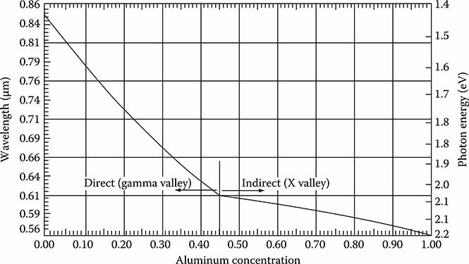
FIGURE 5.16
Minimum energy gap versus aluminum concentration.
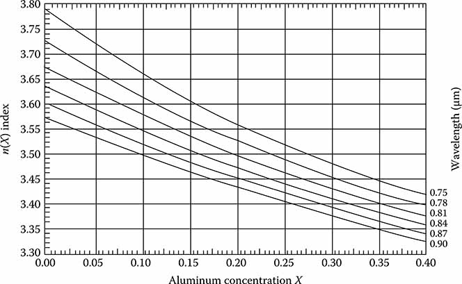
FIGURE 5.17
AlxGa1 −xAs n(X) versus X and vacuum wavelength.
where
r41 is the electro-optic coefficient (for GaAs r41= 1.1 × 10⁻¹² m V−1)
α is an overlap figure with a value between 0 and 1 depending on the overlap of the electric and optical fields
One way to get a larger field overlap is to grow highly conducting n+ layer on top of the SI GaAs substrate before growing the buffer layer. This causes the electric field to be perfectly vertical. It is apparent from the equations that because of the small size of r41 a device structure which can sustain a high electric field is a necessity if unduly long devices are to be avoided.
5.8 Coupling Considerations
5.8.1 Fiber to Waveguide Coupling
The problem of coupling an optical fiber to a waveguide (or a waveguide to a fiber) is critically important to the overall performance of integrated/fiber-optic systems. The most straightforward way of coupling a fiber and a waveguide is the end-fire or butt coupling technique in which the two are aligned end to end and butted into contact (see Figure 5.18). The key factors affecting butt coupling between a fiber and a waveguide are area mismatch between the waveguide cross-sectional area and that of the fiber core, misalignment of the waveguide and fiber axes, and numerical aperture loss (caused by that part of the waveguide light output profile that lies outside of the fiber’s acceptance core or vice versa). In the case of butt coupling of the semiconductor waveguide and a glass laser, reflection at the glass-air-semiconductor interface are also important.
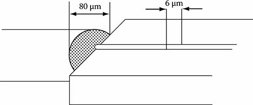
FIGURE 5.18
Butt coupling of fiber to integrated optic waveguide.
In considering coupling of light from the fiber into the waveguide, the problems of area mismatch and numerical aperture loss are limiting factors because the core diameter of a single mode fiber is approximately 4–10 μm and the rectangular waveguide dimensions are 1–5 μm. Exact calculations of the coupling efficiency from fiber to waveguide cannot be done until a particular waveguide and optical fiber have been selected and their characteristics known; however, a typical experimentally observed coupling efficiency for this situation would be about 10%. Robertson et al. [32] have performed a theoretical analysis of butt coupling between a semiconductor rib waveguide and a single mode fiber, and have designed an optimized waveguide structure with a large (single) mode size for which they calculate a coupling efficiency of 86%. However, no experimental data is available.
One approach to the problem of coupling fibers to multiple, closely spaced waveguides is to fabricate a “v-groove chuck” with etched grooves to position and hold the fibers in place, as shown in Figure 5.19. Due to the precision of photolithographic techniques used to etch the grooves and the dimensional precision of standard optical fibers, this method provides a highly accurate means of aligning the fibers and waveguides.
In principle, grating couplers can be used to avoid the problem of area mismatch and numerical aperture loss in coupling between a fiber and a waveguide by providing a coherent distributed coupling over a mutually coupled length of fiber and waveguide. For example, Hammer et al. [33] demonstrated that a grating can be used to couple between a low-index fiber and a high-index waveguide. By embossing an unclad multimode plastic (PMMA) fiber (n = 1.5) over a grating etched into a diffused LiNbxTa(1 − x3) waveguide (n = 2.195), they observed a 6% coupling efficiency. Their calculations indicated, however, that 86% efficiency should be obtainable with an optimally blazed grating. Bulmer and Wilson [34] also used a grating to couple between a single mode fiber and a sputtered glass (Corning 7059) waveguide. In that case the fiber was heated and drawn to reduce the cladding thickness to the point where coherent coupling through the overlapping evanescent mode tails could occur. Again the observed coupling efficiency was low (0.4%), but the authors calculate they could have obtained 30% efficiency if they had used a fiber with a core diameter equal to the width of the waveguide.
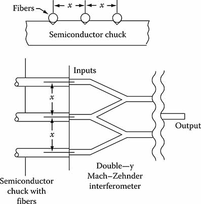
FIGURE 5.19
Fiber input coupling using semiconductor chuck.
5.8.2 Waveguide to Fiber Coupling
Although the same limiting factors are relevant, butt coupling of light from the waveguide to the fiber is an easier task than the converse because the area of the fiber core is larger than the waveguide cross sectional area. In that case a lens can be used to couple more of the light from the waveguide into the fiber. By using a proper intervening lens the effective solid angle of collection can be increased by a factor equal to the ratio of the area of the fiber core to that of the waveguide. By using a cylindrical lens to better match the rectangular waveguide mode to the circular fiber a coupling efficiency of at least 50% should be obtainable [35].
To obtain efficient coupling between optical fibers and waveguides very accurate alignment of the fiber and waveguide is required. Fiber positioning systems are available commercially that provide repeatable accuracy of .1 μm. Automated, production-type, alignment machines that provide 0.1 μm resolution are also available.
5.8.3 Laser Diode to Waveguide Coupling
Hybrid coupling of a discrete laser diode to a semiconductor waveguide can be efficiently done by means of the butt coupling technique. Theoretical studies of laser-waveguide butt coupling [36] indicate that coupling efficiency to a single mode waveguide can exceed 90% if the refractive indices and effective cross-sectional areas of the laser light emitting layer and the waveguide are well matched. Alignment tolerance of less than 0.1 μm is required; however, commercially available piezoelectrically driven X–Y–Z micropositioners are available at reasonable cost that easily meet this requirement. Reliable hybrid butt coupling of an AlGaAs laser diode to lithium niobate waveguide has been demonstrated in the Integrated Optic RF Spectrum Analyzer program [37]. Butt coupling between single mode semiconductor lasers and strip waveguides with a theoretical coupling efficiency of greater than 95% has been predicted by Emkey [38].
Because of the convenience and demonstrated effectiveness of end-butt coupling between the laser and waveguide, it should not be necessary to consider more complicated methods, such as those involving mirrors, prisms, and lenses, for most applications. In addition to being an effective method for coupling laser sources for testing and evaluating waveguide devices, end-butt coupling represents a close approximation to the ultimate coupling of a laser diode monolithically fabricated on the same substrate as the semiconductor waveguide. Thus, evaluation of the characteristics of the hybrid-coupled laser/waveguide combination should provide a good indication of what to expect in the monolithic case.
5.8.4 Waveguide to Detector Coupling
A photodiode detector can be butt coupled to the semiconductor waveguide in the same way described for the laser diode. Ideally one would like an edge-oriented photodiode such as would be used in a monolithically fabricated OIC. Thus, for convenience in testing waveguide devices it is often best to use commercially available, surface-oriented germanium photodiodes. These photodiodes generally have surface areas that are relatively large compared to the cross sectional area of the waveguide; hence, direct end butt coupling results in low coupling efficiency. In this case an intervening lens can be used to compensate for the area mismatch to produce efficient coupling. The 0.7 eV bandgap of Ge results in an absorption edge at 1.55 μm. Thus, a Ge photodiode can be used throughout the wavelength range from 0.8 to 1.3 μm.
5.9 Lithium Niobate Technology
Titanium diffusion into lithium niobate (LiNbO3) is a process used for fabricating waveguides and other devices of an optical circuit. Although LiNbO3 is not an active semiconductor material such as GaAs and hence does not afford the monolithic integration of sources and detectors, much of the work in optical circuit engineering to date has been performed in this material due to the high electro-optic and acousto-optic figures of merit, ease of processing, high optical transparency (<0.1 dB cm−1 total loss from 0.4 to >2 μm), chemical stability, and lack of the requirements for high-level integration and monolithic compatibility. As the ancillary technologies continue to mature, GaAs and semiconductor based optical circuits will continue to supplant the LiNbO3 technology; nevertheless, many of the emerging commercial communications, to be discussed in later sections, are based in LiNbO3.
Selection of the operating wavelength for a LiNbO3 system depends upon many of the same criteria as other material systems. 1.3 and 1.5 μm correspond to the lowest absorption loss wavelengths for silica-based fibers (0.5 and ∼0.2 dB km−1) [39]. The variation of refractive index dispersion which limits the potential modulation rate is also minimized at these wavelengths, so that many of the devices currently available are designed for operation in these regions, along with the AlGaAs source wavelength. At this time the cost and performance of emitters shifts the balance in favor of 1.3 μm except in cases of very long fiber lengths where the lower attenuation at 1.55 μm outweighs these factors. Fluoride fibers currently exist which are capable of less than 1 dB km−1 and theoretically as low as 10−2 dB km−1 at a wavelength of 2.55 μm. Research on InGaAs detectors indicates they make good detectors at that wavelength [40]. Fabrication of these devices is relatively difficult and the cost of fluoride based fiber is higher than silica fibers so the implementation of such a system appears to be downstream.
5.9.1 Electro-Optic and Photorefractive Effects
The electro-optic coefficient translates into the control voltage required for an optical component to function. Typically LiNbO3 devices require very low control voltages with key relations being the following:
Change in refractive index [41]
where
E is the applied electric field (voltage/electrode spacing)
r is the Pockels effect coefficient
R is the Kerr effect coefficient
Optical phase retardation [42]
where
Γ = Ed/V, l = crystal thickness in the direction of the applied field
n1(E), n2(E) are the field dependent indices of refraction
The voltage length for a phase shift VπL is
This is an important parameter as it incorporates the degree of overlap between the optic and electrical fields and must be minimized for low voltage operation.
Another property of LiNbO3 which may be exploited for some devices is the photorefractive effect (a permanent change in the refractive index profile caused by the transmitted optical flux). Optical power levels must be limited to prevent refractive index changes. The effect can be alleviated to a certain degree via the use of longer wavelengths, or it can be exploited in device applications. Integrated optic lenses and reflectors can be fabricated through control of the refractive index. The effect is controllable in LiNbO3 crystals as a function of the impurity levels present [43]. The field spatial change will be of the form
where
ε is the permittivity
k is the photovoltaic coefficient
α is the absorption coefficient
l(z) is the intensity of incident light
D is the diffusion coefficient
e is the charge of an electron
dn/dz is the concentration gradient of free carriers
The first term relates to the ionization of impurities present in the LiNbO3, while the second term describes the current induced by the diffusion of free carriers. Whether the photorefractive effect is a detriment depends on the device application and design.
5.9.2 Photolithography and Waveguide Fabrication
The first LiNbO3 waveguides reported were produced via the outdiffusion of lithium oxide from the crystal lattice from photolithographically defined regions. Although this method was effective at changing the refractive index of selected regions to define the waveguide it tended to produce guides with high losses, and it was only possible to produce multimode waveguides [44]. The high losses have been attributed to lattice imperfections resulting from the outdiffusion [45]. The first devices formed via titanium indiffusion were reported in 1974 [46] and represented a substantial improvement over the existing technology. Devices based on the Ti diffusion process also provide greater possible changes in the index of refraction and less in-plane scattering [47] compared to the lithium oxide out diffused devices.
The fabrication of waveguides in LiNbO3 materials via Ti diffusion is a relatively straightforward process and employs the sequence shown in Figure 5.20 [48]. After surface polishing, areas are defined on the LiNbO3 surface where waveguides are desired, typically by a photolithographic process. Next Ti is deposited over the entire substrate; then, the resist is removed, lifting off the deposited Ti from all but the defined waveguide areas. The Ti is then diffused into the crystal at high temperatures under controlled conditions. Precise descriptions of these individual steps, their significance with regard to device performance, and ongoing research in the related photolithography and diffusion physics will be discussed in the following sections.
The first step in the processing of LiNbO3 for waveguides is surface preparation. The crystal surface must be very flat and low in camber in order to enable the subsequent fabrication of devices with good yields. One of the advantages of LiNbO3 over the other electro-optic materials arises from the fact that it is a strong nonhydroscopic crystal which is easily polished [49]. Another advantage is its availability. Currently high quality substrates of LiNbO3 up to 8 cm long are commercially available [50] so there are cost advantages tied to the use of this material. There are several other ferroelectric materials which offer similar or even slightly better properties [51] but when cost and availability are taken into account LiNbO3 is the preferred choice [52].
After polishing, the LiNbO3 surface is ready for liquid photoresist application. These photoresists are polymeric solutions which are sensitive to certain types of (typically UV) radiation. The polished surface can be coated with resist via spray or dip application, but spin coating is the most common method. In spin coating the substrate is turned very rapidly, up to 5000 rpm, on a turntable as a precisely measured amount of photoresist is poured onto the center of the spinning substrate. This results in a thin, very uniform thickness coating across the surface of the substrate. These resist solutions are only 20%–33% solid so there is a drying step required to drive off all the carrier solvents.
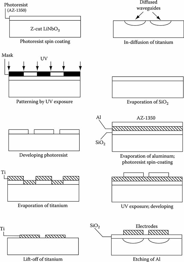
FIGURE 5.20
Fabrication for channel waveguides using Ti:Indiffused LiNbO3.
After drying the resist is ready for exposure. There are two basic types of photoresists: negative acting and positive acting. Both types function via altering of the polymer solubility due to exposure. With exposure in selected areas some regions will be soluble in the developing solutions while others remain insoluble and form the resist surface. In negative acting resists exposure causes polymerization of the material making the exposed regions insoluble. In positive acting resists exposure causes depolymerization, making the exposed areas soluble and thus removable in suitable solvents.
Both resists have some advantages. Negative resists tend to be denser, stronger coatings which stand up better to harsh processing steps. This is because the exposure causes the formation of an interpenetrating polymer network with a much greater degree of crosslinking than in the positive resists. Positive resists generally produce slightly better resolution. This is because they do not suffer the slight shrinkage resulting from crosslinking, nor are they prone to swelling in the developing solutions as with negative resists.
For the standard Ti diffused LiNbO3 waveguides positive resists tend to dominate; however, for some of the newer processes which require a photoresist with greater chemical resistance the negative resists are preferred. Line width control is still a major concern but advances in negative resist chemistry put them almost on a par with positive. Limitations for negative resists under optimal conditions are currently 2.0 μm while for positive resists they are 0.8 μm. Resolution is critical in Ti:LiNbO3 devices in that control and definition of channel width are key to proper waveguide functionality. This is especially true for devices such as Bragg cells where diffraction efficiency is a direct function of waveguide geometry control.
Traditionally both types of resists have required exposure through a suitable patterned artwork or phototool. These phototools contain the desired circuitry or waveguide pattern dependent on the resist type being used. The phototools are typically made of chrome on glass substrates, are very stable with respect to temperature and humidity, and are quite capable of providing the degree of resolution required. They are, however, fragile and expensive as well as time consuming to produce. Often the production of hard tooling can be the most costly and time consuming part of the manufacturing process. An emerging technology that may eliminate the need for phototools is that of direct write lithography. Due to their complexity and density all of the required patterns for producing waveguides are currently generated using computer automated design. This design is then translated from the computer to produce the phototool which is then used to image the pattern onto the substrate. All of these steps represent costs and potentials for error and losses in resolution due to transferring the image from one source to another. In direct write lithography the computer containing the artwork pattern controls a suitable exposure source which is used to directly write the desired pattern onto the photoresist coated substrates without the use of a phototool. In theory these systems could reduce the costs and turnaround times dramatically of prototype, custom, and short run devices by eliminating the need to fabricate hard tools.
There are two methods which may be used to write images: raster scan and vector scan. In raster scan the exposure beam is scanned back and forth across the entire substrate. The pattern is written as a series of pixels by turning the beam on and off as required to define the pattern. In vector scanning the beam only traverses those areas to be exposed. In practice vector scanning has proven to be somewhat faster at scanning a substrate; however, it does require the use of a shaped beam which limits its power compared to raster scanned beams [53].
There are several different types of direct write exposure equipment available, including excimer laser, ion beam, electron beam, and Argon laser system. At this time there is not a preferred system, as all of the systems are capable of producing ultrafine lines and good aspect ratio (height to width ratios), but all are quite slow. Most photoresists currently available are sensitive to radiation in the range of either 365 or 248 nm. This is because most of the optical lithography exposure equipment available exhibits its strongest output peaks at one of these values. Currently available resists require relatively high levels of exposure so that improved resists are required that better respond to the outputs of the direct write systems.
Laser systems using argon laser sensitive resists are in development for certain applications. The new resist films are expected to require only ∼1–5 mJ of energy for exposure, which is about 1/10–1/100 of the current requirement. Another area of research involves the development of a new class of resists based on laser volatilized polymers. These are materials which can be vaporized to CO, CO2, and H2O via exposure to a laser source. The resist coating would be processed as described up to the exposure step, but the laser would selectively destroy the resist as the pattern required. The chief advantage to such a system is that it would eliminate the need for a developing step.
After exposure, development, and a final bake (to increase crosslink density) the imaged LiNbO3 substrate is ready for further processing. The next step is the coating of the piece with titanium. This may be accomplished via resistance heated evaporators, sputtering, or electron beam process (see Figure 5.21) [54]. This step produces a uniform metal layer deposited over the entire piece. The thickness of the Ti coating is determined by the deposition rate and contact time. The coating thickness is critical in that it is a key parameter in determining the diffusion depth and concentration. Typically the metal will be deposited to a height of 0.3–1.0 μm depending on the wavelength of operation and the degree of confinement of the waveguide. Ti metal will be in direct contact with the LiNbO3 only in those channels opened up by the photolithographic process. The next step is the lift off or stripping of the resist. The Ti coated piece is immersed in a suitable solvent that attacks the polymerized resist causing it to disintegrate and the Ti adhering to it to lift or wash off. The resist’s aspect ratios become important at this point in that the resist must be substantially thicker than the Ti coating. If not, the metal coating adhered to the LiNbO3 can bridge over and become adhered to metal covering the resist, which results in a phenomena known as mushrooming (see Figure 5.22). This can result in poor line definition and ultimately in poor device performance.
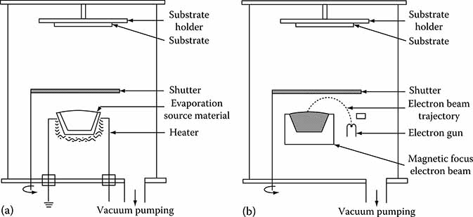
FIGURE 5.21
(a) Resistance evaporation and (b) electron beam evaporation.
Titanium indiffusion is the next key area in the fabrication of a LiNbO3 waveguide device. Extensive research continues in this area to characterize more fully the exact nature of Ti diffusion into the material and to more predictably control the diffusion. The current preferred process is to indiffuse the Ti at a temperature of 980°C–1050°C for 4–12 h. The diffusion must be performed under tightly controlled atmospheric conditions to prevent the out-diffusing of LiO3 which can accompany metal indiffusion. The first LiNbO3 waveguide devices were fabricated by taking advantage of the outdiffusing of LiO3 at high temperature [55]. With the current technology this outdiffusing is considered to be a major problem as it can result in the formation of surface waveguides outside the channel regions [56].
Molecular diffusion is a means for mass transfer which results from the thermal motion of molecules and is limited by collisions between molecules. The first step in understanding the diffusion process is to develop an understanding of Fick’s Law
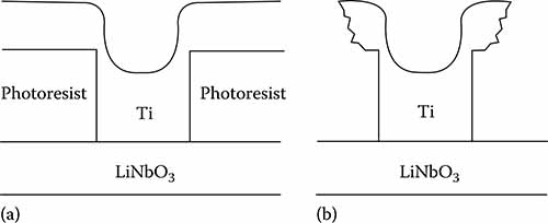
FIGURE 5.22
(a) Ti coated over photoresist with and insufficient aspect ratio and (b) “Mushrooming” noted after resist stripping.
for one dimension, and
for three dimensions, where dn = amount of a substance diffusing, q = cross section (along x-axis), −dc/dx = concentration gradient, dt = time, and D = diffusion constant. This states that an amount of some substance (dn) will diffuse through a cross section (q) along the x-axis in a time (dt) so long as a concentration gradient exists, and that the amount is governed by a diffusion constant. As the concentration gradient goes to zero (i.e., complete uniformity) the diffusion falls off to zero. Diffusivities in solids cover a wide range of values and are typically quite low for dense crystalline materials such as LiNbO3. A material diffusion constant (D) is not a universal constant but is rather a constant for specific situations and conditions. Diffusion coefficients are unique to individual materials and are a strong function (usually linear for solids) of temperature. For crystalline materials such as LiNbO3 multiple diffusion coefficients exist depending on the plane of interest [57]. As molecular diffusion is limited by collisions between molecules these planar variations are expected.
Fick’s Law is merely a general statement of diffusion theory and, although it cannot be violated, many specific forms of the law exist and apply to different situations. For diffusion of Ti into LiNbO3 the diffusion depth, as expected from Fick’s Law, is a function of the material diffusion constant, the diffusion time, and the diffusion temperature. The diffusion profile has been found to be roughly exponential, and more specifically the Ti concentration has been found to follow a Gaussian distribution [58]:
where
c(x3, t) is the Ti concentration in the LiNbO3 crystal
t is the diffusion time
τ is the thickness of Ti coating prior to diffusion
Dy is the anisotropic diffusion coefficient (temperature dependent)
The general form of the temperature dependent diffusion coefficient is
where
T is the crystal temperature
E is the activation energy
For Ti diffusion into LiNbO3 the temperature dependent D has been found exponentially to be [59]:
where
T is the absolute temperature
T0 = 2.9 × 10⁴
Dy0 = 7 × 10⁻³ cm2/s
The form appears logical since E can be expected to be quite low at the surface, yet increasing with diffusion depth. For this type of diffusion, depth dependent diffusion coefficients are being pursued via mathematical modeling [60]. These are particularly valuable in explaining the lateral surface diffusion which is often observed in the fabrication of these devices [61]. One particular phenomena which greatly benefits these devices results from the lower observed lateral diffusion rates. It has been noted that the diffusion of Ti down (vertical) into the LiNbO3 crystal is about 1.5 times the horizontal diffusion rate (dependent upon the orientation of the crystal) [62]. This enhances the quality of the channels being formed and ultimately the devices being fabricated.
As seen from the equation the Ti diffused into the crystals is a linear function of Ti thickness; thus the Ti thickness can be used to determine the refractive index change. This assumes that all of the Ti is indiffused during the diffusion time (t). A proposed equation for this relation is [63]
where
dn/dc is the change in refractive index with concentration
α is a proportionality constant
This change has been found to be dne/dc = 0.47 and dn0/dc = 0.625, where ne and n0 are extraordinary and ordinary refractive indices. For a specific wavelength the diffusion depth (D*) is of the form
This shows that all the important parameters for defining the waveguide may be controlled within fabrication. Waveguide width is defined via photolithographic techniques, depth is controlled via diffusion time, and change in index of refraction of the waveguide versus the surrounding crystal is a linear function of the deposited Ti thickness.
There is an additional process step involved in the actual mechanism of diffusion. It has been discovered that Ti does not directly diffuse into the LiNbO3 crystal but rather goes through an intermediate oxide phase before entering [64]. Important intermediate products are TiO2, LiNb3O8 and (Ti0.65Nb0.35)O2 [65]. It has been noted experimentally that if the deposited Ti layer is first oxidized at temperatures of 300°C–500°C for approximately 4 h the resultant waveguides display better performance characteristics with regard to energy loss due to in-plane scattering [66]. It has been noted that this oxidation step should be done in an O2 or dry air atmosphere [67] to prevent the excess stripping of O2 from the LiNbO3 crystal, and to prevent the formation of faults within the crystal [68]. It has been found that following complete TiO2 formation a LiNb3O8 phase forms [69]. These two may then combine to form (Ti0.65N0.35)O2. The latter ternary compound begins to form at temperatures above 700°C and its formation rate increases up to 950°C. This compound has been identified as the true source of Ti for diffusion into the LiNbO3 crystal, the ultimate compound being (LiNb3O8)0.75(TiO)0.25 wherein counter current diffusion of Nb+5 and Li+1 and indiffusion of Ti+4 occur.
The LiNb3O8 appears to be the resultant of Li or LiO2 outdiffusion, and will form at temperatures of 650°C < T < 950°C regardless of whether or not Ti is present. As stated previously outdiffusion of Li or LiO2 causes changes in the index of refraction. The uncontrolled outdiffusion of these compounds in Ti indiffused waveguides is a major concern. This is because if left unchecked surface waveguides (the equivalent of electrical shorts) could form and limit the usefulness of the device. A number of studies have been undertaken [70] on the nature of structural faults which occur during the formation of Ti:LiNbO3 waveguides. What is typically noted is that Li does outdiffuse and Nb molecules take their place in the waveguide portion of the crystal. Vacancies exist where the Nb had been. The faults are present in undoped (no Ti) Li deficient waveguides as point defects. In Ti indiffused systems they tend to form structural faults on the order of tens of microns [71]. Faults of this size are possible scattering sights for photons and thus their formation must be controlled. The growth kinetics of LiNb3O8 may be controlled via annealing of the waveguide in an atmosphere rich in Li in the presence of O2 or in an atmosphere of steam [72]. Typical device parameters for the formation of a Ti:LiNbO3 waveguide device would require channel widths of 8–10 μm, a coated metal (Ti) thickness of 0.3–1.0 μm, diffusion temperature of 980°C–1050°C, and a diffusion time of 4–12 h. This results in diffusion depths on the order of 5–10 μm. This process is used to form waveguides for operation in the 1.3–1.55 μm wavelength range where common silica-based fiber exhibits its best properties. Propagation losses as low as 0.2 dB cm−1 have been noted in waveguides produced via these techniques [73]. After diffusion the crystal end faces are polished to allow for coupling to a fiber. Waveguide devices for operation at a wavelength of 2.6 μm for use with the ultra low-loss fluoride based glass fiber have also been developed [74]. For these devices the optimal channel width is 13–15 μm, the required thickness is 0.8 μm, and the diffusion conditions are 1050°C for 12 h.
5.9.3 Implantation and Proton Exchange Techniques
A great deal of research continues with the goal of supplementing or replacing Ti diffusion. One technique is to ion implant Ti into the LiNbO3 crystal. The waveguides regions are defined lithographically and implanted. This causes an amorphous layer to form in the waveguide regions. Solid phase epitaxy is then used starting from the undamaged underlying LiNbO3 substrate in order to restore crystallinity and produce a functional waveguide. This process produces good waveguides with higher Ti concentrations and, therefore, greater changes in index of refraction than are possible via thermal diffusion [75]. It also promises sharper geometries and tighter Ti concentration gradients than are otherwise possible.
Another means for altering the index of refraction of LiNbO3 is proton exchange. In this process the crystal (with defined waveguide regions) is submersed in a solution of benzoic acid at a temperature of 210°C–245°C for 1–4 h. The benzoic acid is the proton (H+) source and the diffusion of protons into the substrate causes the index of refraction to rise in those areas [76]. The process has the advantage of being a simple low temperature process, and is capable of achieving greater changes in the index of refraction than with Ti indiffusion. The drawback is that devices fabricated in this manner typically cannot achieve the same performance levels (losses) as LiNbO3 devices. Annealing after the proton exchange improves the optical quality but also causes a drop in the achieved index of refraction.
Another exciting fabrication technique is known as Titanium Indiffused Proton Exchange (TIPE). This technique has the capability to produce devices not possible by either TI of PE processes alone. In TIPE a standard Ti indiffusion process is first applied to the LiNbO3 substrate to define some regions with higher indices of refraction. The piece is then masked with a suitable image and immersed in a benzoic acid solution. This results in the areas of the crystal exposed to both Ti indiffusion and PE having relative indices of refraction considerably greater than achieved by either process alone. The most important and immediate application for this technology is in the fabrication of planar waveguide microlenses [77] (Figure 5.23a and b) and microlens arrays. Desirable properties of TIPE lenses include: very short focal lengths, large numerical apertures, small focal spot size, and low insertion losses [78]. The utility of these TIPE lenses has already been demonstrated via the production of an integrated acousto-optic Bragg modulator module on a LiNbO3 substrate. Some preliminary testing utilizing the modulator for optical systolic array processing has also been undertaken [79]. These devices are expected to greatly facilitate the development and implementation of integrated and fiber-optic signal processing and computing.
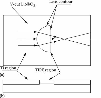
FIGURE 5.23
Planar waveguide lens in LiNbO formed by titanium-indiffused proton-exchange technique (a) top side, (b) side view.
5.10 Semiconductor Waveguide Fabrication Techniques
A wide variety of methods are used to fabricate optical waveguides and components. These include thin-film deposition, epitaxial growth, filled channel techniques, ion diffusion, and ion implantation. Several of these techniques have been discussed in other sections. This section covers the techniques most conducive to integration and production of optical circuits—namely, MOCVD, MBE, and ion implantation—along with a discussion on foundry facility utilization.
5.10.1 Ion Implantation
Ion implantation is a particularly valuable technique that offers a number of distinct advantages in comparison to the other fabrication methods [80]. In ion implantation a beam of atoms is ionized, accelerated to kinetic energies up to several million electron volts, and directed at a suitable material target. The resulting damage in the material and the introduction of foreign atoms can produce electronic, chemical and optical changes. The primary advantage of this technique lies in the precise external manner by which doping of materials can be controlled. Any known species can be introduced into a given material, and the dopant concentration is not limited by ordinary solubility considerations. (However, the concentration of dopant atoms occupying substitutional lattice sites is generally limited by the solid solubility.) The dosage can be monitored accurately and the depth profile of the implanted ions can be controlled by adjusting the implant energy. This permits realization of dopant profiles that could not be achieved by diffusion or any other technique. Also, implantation of materials can be performed over a wide range of temperatures, allowing unique interactions of the implanted ions. Precise device configuration is achievable due to the parallel development of high resolution GaAs lithography and masking, and through proper control and selection of the ion beam energy and fluence and the substrate doping level.
Ion implantation can produce a change in the refractive index of a crystalline semiconductor material through various physical mechanisms [81]. These mechanisms include damage to the crystal lattice, ultimately resulting in an amorphous region; introduction of dopant atoms into the lattice, causing a change in the polarizability of the unit cell; localized regions of stress in the lattice due to damage and the presence of a large number of dopant atoms in these regions; and the compensation of the free carriers in suitably doped materials. This last mechanism has been the primary method used to form optical waveguides in semiconductor materials through ion implantation. Of course, in any actual implementation the mechanisms are interrelated, and the change in the index of refraction of the implanted materials is due to the total effect of these processes. It is possible, however, to accentuate one of the mechanisms and to minimize the effects of the others. The most common ion species utilized for GaAs optical device fabrication is the proton (H+). These ions produce the least amount of damage to the crystal and minimize the contributions to the optical properties arising from the physical processes other than free-carrier compensation. Protons also are unlikely to occupy substitutional sites in the lattice and have the greatest projected range by direct energetic penetration without relying on any secondary or defect diffusion.
5.10.2 Ion-Implanted Semiconductor Annealing
As discussed in Laser Annealing of Semiconductors [82], the abrupt recrystalization process upon annealing ion-implanted silicon in the temperature range 500°C–600°C is in contrast to the more complex multistage process in the solid phase annealing of ion-implanted GaAs. Several publications [83] illustrate that damage removal of ion-implanted damage in GaAs occurs over a broad temperature range.
The nature of the solid phase annealing process was further revealed [84] as shown in Figure 5.24. Measured GaAs disorder, obtained from Rutherford backscattering-channeling spectra, was plotted as a function of the anneal temperature following an amorphizing implant of 8 × 10¹³ Ar cm−2 at 100 keV. These data revealed two apparent annealing stages, the first occurring rather sharply in the temperature range 125°C–230°C (for 15 min anneals), followed by a second stage in the range of 400°C. Channeling cannot unequivocally reveal the nature of the residual disorder but, from observations of characteristic color changes during annealing, Williams and others [85] suggested that stage-1 recovery related to defects corresponding to amorphous regions in the crystal. Kular [86] correlated channeling, TEM, and electrical measurements, and indicated a third anneal stage in which the density of loops was progressively reduced.
FIGURE 5.24
Normalized disorder, as measured by channeling, for 100 keV 8 × 10¹³ Ar cm−2–implanted (100) GaAs plotted as a function of furnace annealing temperature (15 min anneals), indicating two annealing stages. (From Williams, J.S. and Harrison, H.B., In Laser and Electron Beam Solid Interactions and Material Processing, Gibbons, J.F. et al, eds., North-Holland Publishers, New York, 1981, p. 209.)
Of further significance are measurements of electrical activity of ion-implanted GaAs that show continual improvement up to 9000°C [87]. In view of the anneal process described, the best electrical behavior is at least contingent upon the complete removal of crystal defects that arise during the low temperature annealing of implanted GaAs. This is not to suggest that complete removal of crystalline dislocation loops is sufficient to guarantee good electrical behavior. Other factors may certainly influence the electrical properties, following furnace annealing, such as point defect clusters and material impurities, particularly Cr distributions, and the nature of encapsulants used to protect the surface from decomposition.
Pulsed laser annealing of ion-implanted GaAs received considerable attention from several laboratories [88]. These studies indicated that uncapped wafers be laser processed in air at room temperature to provide good crystallinity, high substitutionality of implemented ions, and electrical activities superior to those achievable by conventional furnace annealing although, under certain conditions, decomposition of the surface was a problem.
Williams compared [89] the effectiveness of CW laser and furnace annealing in the removal of amorphous implant damage in GaAs, and found that both CW (argon ion) laser and the low-temperature furnace anneal produced good amorphous-to-crystalline recovery (stage-1 annealing). It became apparent, in both the pulsed and CW laser annealing experiments, that many of the problem areas associated with furnace processing of GaAs either remained as difficulties or gave way to significant problems associated with rapid heating and cooling effects [90]. Results obtained from both furnace annealing and the various transient annealing methods for implanted GaAs are summarized in Figure 5.25 [91]. Since generally only simple point defects are produced on implanted GaAs, with no extended defects or loops, only first-stage annealing (125°C–230°C) provides an effect, which is advantageous to optical performance.
5.10.3 MOCVD: Growth and Evaluation
MOCVD and MBE are discussed and contrasted in an earlier section on material growth. Recent improvements in crystal growth capabilities and heteroepitaxial deposition of very low defect density structures, using either MOCVD or MBE, have significantly advanced the optical circuit device producibility and performance factors.
Figure 5.26 illustrates the operation of the vertical atmospheric-pressure MOCVD reactor [92]. In this technique, “vapor-phase mixtures containing the metalorganic compounds are pyrolyzed at or near the surface of a heated substrate, where they combine to form the deposited layer. Most sources are liquid near room temperature with relatively high vapor pressures, and so may be carried to the reaction zone by bubbling a carrier gas such as high purity hydrogen through the liquid source” [93]. As an example, GaAs is usually grown using trimethylgallium plus pure arsine gas producing GaAs and carbon tetrahydride (CH4) by-product. “Deposition proceeds as reactants decompose in a stagnant boundary layer just above the surface of the wafers.” Commercial equipment is capable of processing up to twelve 3 in. wafers in a single processing cycle and up to three processing cycles may be completed in a production shift.
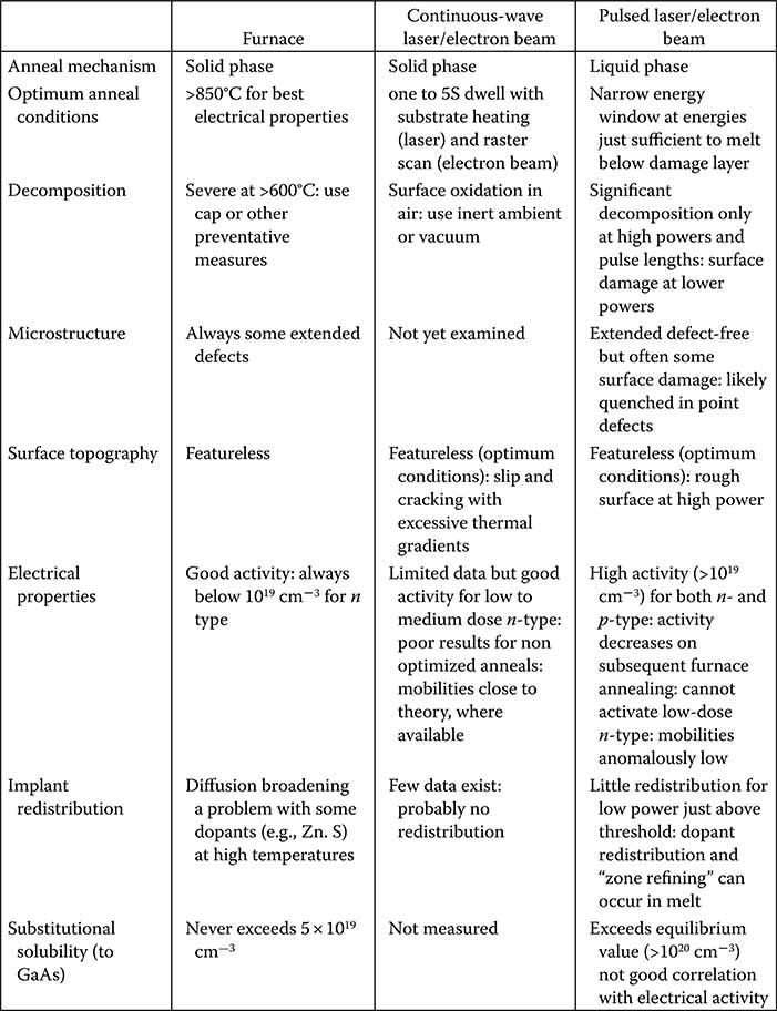
FIGURE 5.25
Comparison of the various annealing methods for ion-implanted GaAs.
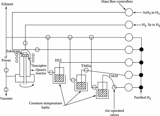
FIGURE 5.26
Vertical atmospheric-pressure MOCVD reactor.
The aluminum composition (x) of the alloy is determined from the peak energy of the band-edge emission of photoluminescence spectra for single layers. A special facility can profile the photovoltage of a multilayer structure at the same time that a carrier profile is obtained by electrolytic removal of material in conjunction with computer controlled capacitance-voltage determinations. Deep level traps in the material are investigated by the Deep Level Trap Spectroscopy (DLTS) technique and other related measurements.
5.10.4 MBE: Growth and Evaluation
Molecular beam epitaxy, which involves the reaction of one or more thermal beams of the desired atoms or molecules with a crystalline substrate under ultrahigh vacuum conditions (10−10–10−11 Torr background, 10−6 Torr operating pressure), can achieve precise control in chemical compositions, doping profiles, and layer thickness. A typical MBE system for growth of GaAlAs is shown in Figure 5.27. Uniformity of chemical composition and doping profile are typically better than 1% with thickness variations less than +0.5%. An additional advantage is that no high temperature processes are required, so that very minimal bulk diffusion effects occur. Single-crystal multilayer AlGaAs atomic layers can be grown by MBE. Atomically smooth growth surfaces allow complex doping and compositional structures and synthesis of artificial materials with prescribed characteristics.
FIGURE 5.27
A typical MBE system for growth of AlGaAs.
Characterization of MBE samples occurs first during growth with the in situ capability of RHEED and Auger electron spectroscopy which provide information for growth conditions, allowing preparation of high quality samples. After growth of samples, x-ray diffraction and electron microscopy provide information on crystal structure, crystal orientation, and crystal perfection. Transport measurements provide information concerning carrier concentration and mobility. Raman spectroscopy can provide information regarding the quality of interfaces.
Complex optical circuit structures require epitaxial layer uniformity and precision in thickness, doping, and AlGaAs composition. Depending upon the particular design, there are advantages to both MOCVD and MBE. Tables at Figures 5.28 and 5.29 compare material properties, parameter controls, and system cost for the two techniques.
5.10.5 MBE Development in Space
Past and present experience in submicron optoelectronic and electronic devices employing single crystal GaAs in epitaxial interface with single crystal AlGaAs has clearly indicated that the limiting criteria for optimal device performance is the purity of the AlGaAs. Even under the best starting condition vacuums available on earth (10−11–10−12 Torr), there exist serious defects caused by impurity atoms and by water vapor as well as Co2 and O2. Such impurities adversely affect the energy gap of the AlGAAs and the epitaxial match lattice parameters for single crystal growth and interface requirements, as well as adversely altering doping carrier concentrations and establishing unwanted localized or delocalized energy band states.
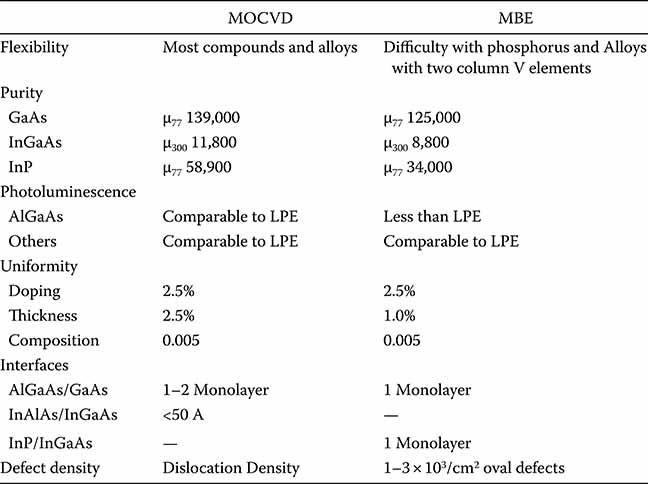
FIGURE 5.28
MOCVD versus MBE—Comparison of Material Properties. (From Dapkus, P.D., J. Crystal Growth, 68, 345–355, 1984.) [94]
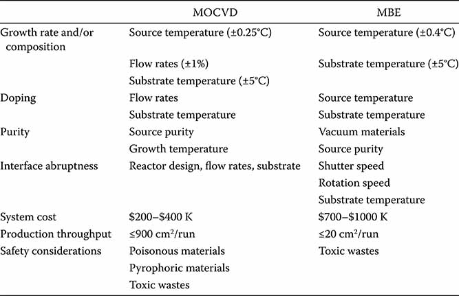
FIGURE 5.29
MOCVD versus MBE—Comparison of parameter controls and system cost. (From Dapkus, P.D., J. Crystal Growth, 68, 345–355, 1984.) [94]
Growth of optoelectronic waveguides and submicron devices in the ultrahigh vacuum conditions (10−14 Torr) behind the wake shield of the NASA Space Shuttle (a working volume of about 50 m3) or a space-based manufacturing facility will greatly enhance device performance. Improved performance factors include superior confinement of the exciton cloud in the layer of lower Eg for ultra-fast switching and modulation of optical quantum well devices; better homogeneity of layers and waveguides, and constancy in the mismatch of refractive indices throughout the waveguide boundary interface of an optical coupler of interferometric device; and improved gain characteristics of high electron mobility transistors.
5.11 GaAs Foundry Capabilities
About 25 years ago the first GaAs ICs were introduced in the form of microwave prescalers. A parallel may be seen between the development of silicon based industries and the growth pattern of the GaAs industry. First came the transistors, then simple logic applications such as flip-flops, and from this arose full multifunction monolithic capability. At this point, high quality GaAs substrate material is being achieved and several foundries are in mass production of MMICs for the microwave industry. A major application of this MMIC technology centers on the need for low cost highly reliable microwave components for Phased Array Radar Transmit/Receive Modules. Optical applications of MMIC technology are discussed in a later section. MMIC processing and foundry capabilities are directly applicable to the requirements and problems of optical device fabrication.
Several wide bandwidth functional building blocks are available for design use, including switches, phase shifters, and medium performance amplifiers, with the GASFET being the key building block. Applications and the GASFET technology are discussed further in a later section. The designer will save valuable development time and money by adjusting the circuit architecture to take advantage of available functional blocks. While the discrete GASFET manufacturers are producing devices for low noise applications with gate lengths of less than 0.3 μm. MMIC foundries are capable of routinely producing only 0.5 μm FETs, restricting the microwave designer to a “medium low noise amplifier” (implying a noise figure of 3 dB at 12 GHz, for example). Heterostructure devices, such as the high electron mobility transistor (HEMT), are currently in production at MMIC foundries.
Many foundries still produce three inch wafers as standard. The hope is that eventually the growth of high purity GaAs in larger diameter slugs will help raise processing yields and lower the cost of MMIC devices. One way in which MMIC manufacturers are increasing their yield percentages is by the use of process control monitors (PCMs) on the wafers. By using PCMs in conjunction with specialized test equipment that has been developed specifically for MMIC production purposes, manufacturers are able to pull bad wafers from the production line before too much time and effort has been spent on processing a wafer that will not yield a profitable amount of useable MMICs. Electrostatic discharge of the GaAs devices is accomplished by integrating shunt diodes onto the die at the device inputs and outputs.
In designing an optical circuit employing monolithic microwave devices, the devices used in the design must be within the standards set by the foundry chosen to manufacture the chips. The use of computer-aided design (CAD) and computer-aided engineering (CAE) tools for the MMIC portion of the system usually produces significant cost efficiency. Fraser and Rode of Triquint Semiconductor have published a list of design strategies they feel will provide a firm basis for efficient and reliable MMIC designs. A few of the major points from the list follow [95]:
MMIC costs are not based on the number of FETs used in the design, so they should be used freely.
MMIC is best suited for medium performance functions; circuit complexity is inversely proportional to the yield.
Start with simple designs to prove concepts and then move on to more complex topologies.
The use of lumped elements below 18 GHz will reduce circuit size without sacrificing performance.
Make use of the standard cell libraries provided by the foundry to avoid reinventing the wheel.
Design for testability by providing ample test points at easy to access places on the wafer.
During computer optimizations of the design it is imperative that the effects of process variations and material spreads are included.
A typical MMIC design sequence from performance definition through the foundry layout review is as follows [96]:
Define MMIC performance requirements.
Select the basic circuit and layout topology.
Simulate circuit performance using CAE techniques.
Analyze the design over temperature and process variations.
Optimize the design and do a rough circuit layout.
Calculate the device parasitics and incorporate them into the design.
Re-optimize the design over temperature and process variations.
Run the circuit through a design rule checker to ensure that none of the basic layout rules have been violated.
Conduct a layout review at the foundry.
Computer analysis and synthesis software has been developed to meet the needs of the microwave designer by a number of sources. Companies are now providing the software packages that enable the engineer to design circuitry, perform analysis and optimization functions, and transfer layouts. In addition, they furnish the user with foundry libraries to enable simulation of a MMIC implementation of the user’s circuitry. Figure 5.30 [97] indicates the range of CAE/CAD software available from one manufacturer and demonstrates how this software fits into a systematic design flow.
After the design sequence is completed the foundry is generally assigned the task of generating the masks required to produce the finished wafer. After the wafer is produced, the foundry test facility is able to run tests on the various dies on the wafer according to test points that have been made available by the designer. A typical test setup [98] for wafer testing is shown in Figure 5.31.
FIGURE 5.30
EESOF product suite. (After Parrish, P. of EESOF, Computer-aided engineering in GaAs monolithic technology, Monolithic Technology, October 1987.)
FIGURE 5.31
Typical wafer mapping test station. (After Dammann, C. et al., Microwave die sort and wafer mapping for GaAs MMIC manufacturing, Monlithic Technology, October 1987.)
FIGURE 5.32
Typical wafer test station display. @ = high current, # = low current, % = bad rf, & = low gain, * = high refl, $ = passed.
With this configuration, the operator may run a variety of DC and RF tests which generate a computer display similar to that [99] depicted in Figure 5.32. With this information stored in the system controller, the good dies may be scribed and separated from the unusable. If this prototype hardware passes testing, the design may go to production. If the design is flawed, then the design layout, mask generation, and prototype manufacturing cycle must be repeated.
The cost of a single foundry prototype run, including mask generation, is generally between thirty and fifty thousand dollars depending upon the process required [100]. Although this is expensive, twenty to thirty designs can be integrated on one mask so that the cost per MMIC design may be as low as two to three thousand dollars. Once in production, the cost per wafer will drop by more than an order of magnitude. A failure rate of one GaAs FET per 2 × 10⁶ h may be expected for newer medium-integration products [101]. This rate is lower than the failure rate for discrete GASFETs. This result is in accordance with trends established for silicon ICs [102]. At 125°C channel temperature, and with current densities within the limits of the design rule checker, the failure rate of a standard MMIC design should be less than 0.01% per 1000 h [103].
As technical advances in this arena continue, submicron capability becomes cost effective. Submicron gate length FETs promise lower noise figures and increased sensitivity of microwave receivers. By increasing the standard wafer size and tightening manufacturing process controls, higher yields per wafer and lowered MMIC cost are realized. Integration of HEMT processing into the MMIC arena aids in the expansion of MMICs into the millimeter wave frequency band.
5.12 Emerging Commercial Devices and Applications
Dozens of companies worldwide are currently offering integrated optical circuits and components. Many operate pilot production lines for a wide range of components. (Use of pilot production or foundry facility for development of custom OICs was discussed in an earlier section.) Many of these companies are already well established in the related materials, optical communications, and defense system technologies. The components in the market target a wide range of applications, including the following:
Telecommunications (line-of-sight and fiber optic)
Optical computing
Laser range finding
Optical proximity fusing
Fiber sensors
Target designation and tracking
Industrial measurement and control
Optical interconnects
Medical instrumentation
In particular, currently available components perform various critical functions in fiber-optic communication and sensing systems, such as modulation (phase and intensity), switching, mode conversion, splitting/coupling, and signal processing. Many of the companies offering integrated optic devices concentrate on the LiNbO3 and glass technologies, but a wide variety of silicon and compound semiconductor devices are available as well.
Because of the range and diversity of applications for integrated optics, estimates of the markets are difficult to project. Many companies and R&D labs have custom capability but do not advertise. Companies typically advertise a year or two ahead of availability. One set of predictions [116] estimated a total integrated optical circuit market of $5M in 1987, growing to $100M in 1990, and to $500M by 1995. Eighty percent of the 1990 market was predicted to be LiNbO3 devices, but 50% of the 1995 market would involve compound semiconductor devices. The applications are predominantly in the fiber sensor, communication, switching, biomedical, and instrumentation areas.
The integrated optical product data shown in Figure 5.33 through 5.41 was supplied by a number of the companies initially offering commercial devices 20 years ago. These are representative of the technology available from a number of sources. Direct performance comparisons are not made, since specific applications will determine the most suitable device. Specific device characteristics should be obtained from manufacturers.
Future systems requirements are as diverse as the applications to be addressed. Critical components include tunable lasers, optical routers and high density crossconnects, wavelength converter devices, optical switches, add-drop multiplexers, amplifiers and transceivers, fiber gratings, equalizing filters, bandwidth management, circulators, modules, and integrated packages, and a range of interface components and connectors. Successful developers require flexible material systems and technology approaches. Integration of key functions on planar optical platforms improves reliability and lowers ultimate integration costs. Mixed optic and electronic solutions best adapted to market needs provide the optimum strategy. Fiber grating devices providing optical networking enhancements include switches, adjustable filters, network monitors, add-drop filters, gain flatteners, and dispersion compensators.
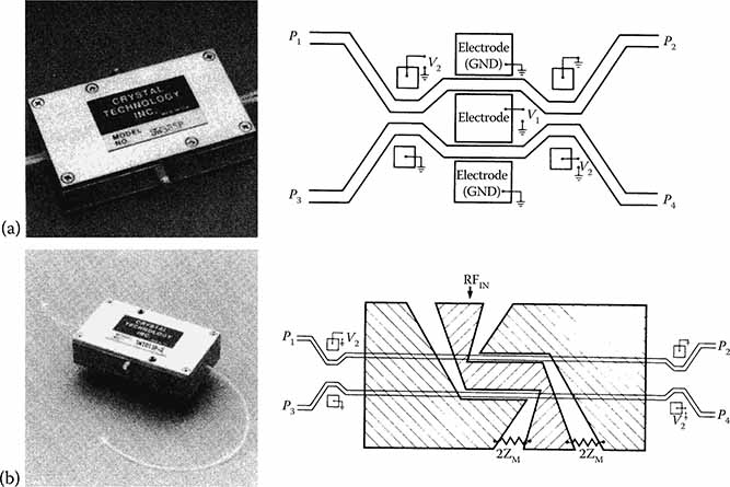
FIGURE 5.33
(a) LiNbO3 2 × 2 switch, (b) LiNbO3 traveling wave 2 × 2 switch.

FIGURE 5.34
LiNbO3 phase modulators.
5.12.1 Fiber-Optic Couplers
The most successful coupler manufacturing technology to date is the fused biconical taper (FBT) process. This involves placing two center-stripped fibers close together in a fixture and heat stretching the glass over a hydrogen-oxygen flame until a fused region is created. This is performed while monitoring the optical power through the fibers until a desired optical performance is achieved. The fused region is then packaged in a stable substrate.

FIGURE 5.35
(a) KTP phase modulator; (b) LiNbO3 Mach–Zehnder intensity modulators (Courtesy of British Telecom & Dupont [BT&D Technologies], London, U.K.); (c) (Courtesy of Pilkington Guided Wave Optics & Barr & Stroud, Ltd., Glasgow, U.K.); (d) (Courtesy of Crystal Technology, A Siemans Company, Palo Alto, CA.)
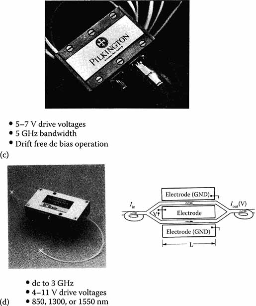
Technical and sales leaders included Gould, ADC, Corning, FBT, E-Tek, Aster, IOT, IOC, and AMP. Gould is the inventor of the FBT process and holds some of the key patents. Manufacturing was transferred to Swiftlink in India, who supplies dual window (1310/1550) FBT components. Corning patented a multiple index coupler, where a circular glass substrate is applied around the fibers during fusion. This is claimed to be more stable, but is more complex. E-Tek designed and developed an automated coupler workstation, with excellent repeatability and polarization dependent loss.
The manufacturing technology for FBT is quite challenging. FBT devices are relatively large and require significant packaging design for stable operation. At best, this technology can support six fiber ports with reasonable port-to-port uniformity and optical performance. Port counts of higher than six require fusion splicing and bulky enclosures. FBT devices require dedicated workstations and groups of operators fabricating one fused region at a time although recent efforts to automate the process show promise. Average daily yields often do not exceed 70%.
5.12.2 Performance Testing Issues for Splitters
The optical parameters most often tested are the following:
Split ratio—this is the percent of optical power measured at an output fiber compared with the total output power. This is also measured as insertion loss in dB. Most splitters are 50/50 equal split.
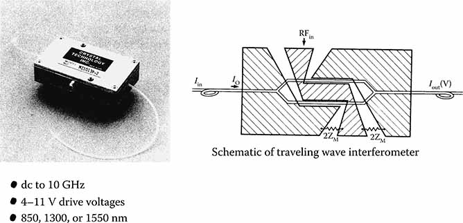
FIGURE 5.36
Traveling-wave intensity modulator. (Courtesy of Crystal Technology, A Siemans Company, Palo Alto, CA.)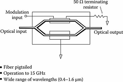
FIGURE 5.37
KTP Mach–Zehnder modulator.Excess loss—the amount of optical power lost in a device, in addition to the insertion loss.
Passband—the wavelengths at which the performance specifications apply. Splitters are generally highly wavelength sensitive.
Directivity—the amount of power reflected relative to the input power to a device, measured exiting an input fiber. FBTs typically exhibit better than 60 dB directivity.
Isolation—when a splitter is used as a demultiplexer, isolation is a measure of the coupler’s ability to separate two or more wavelengths. Isolation is usually measured as a dB difference in the measured optical power of one wavelength compared to another.
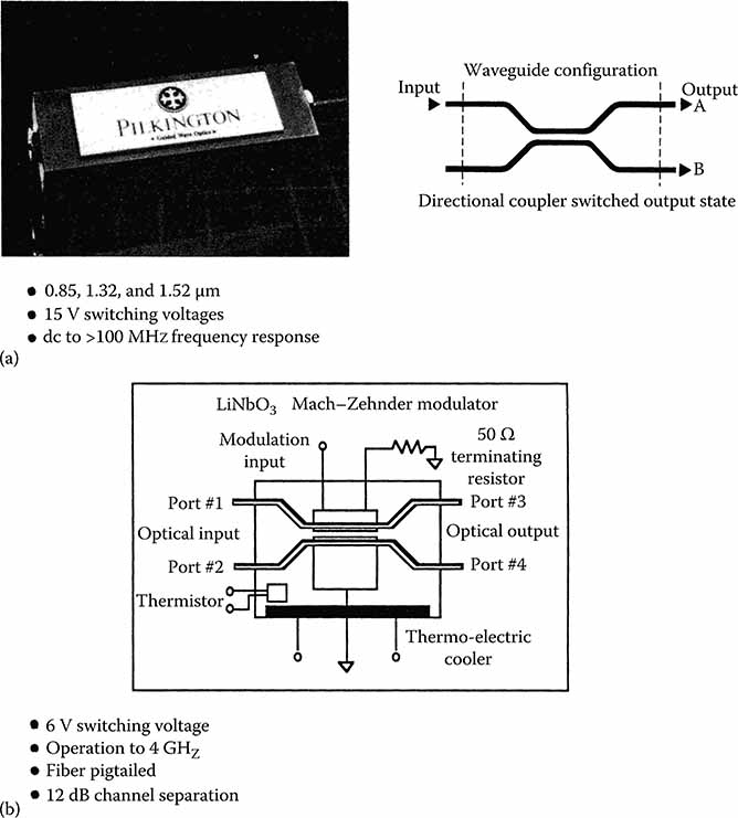
FIGURE 5.38
LiNbO3 directional couplers modulators. (a) (Courtesy of Pilkington Guided Wave Optics); (b) (Courtesy of Barr & Stroud, Ltd., Glasgow, U.K.)Uniformity—most often used with more than two fiber I/O ports, uniformity is the maximum difference in insertion loss in dB from one port to another.
Polarization—also designated polarization dependent loss (PDL) in splitters. The optical power transmission of fiber-based devices is often dependent on the orientation of the electromagnetic wave entering the device. PDL is a measure of how insertion loss changes as the orientations or states of polarization (SOP) change. In most quality devices, PDL measures less than 0.2 dB.
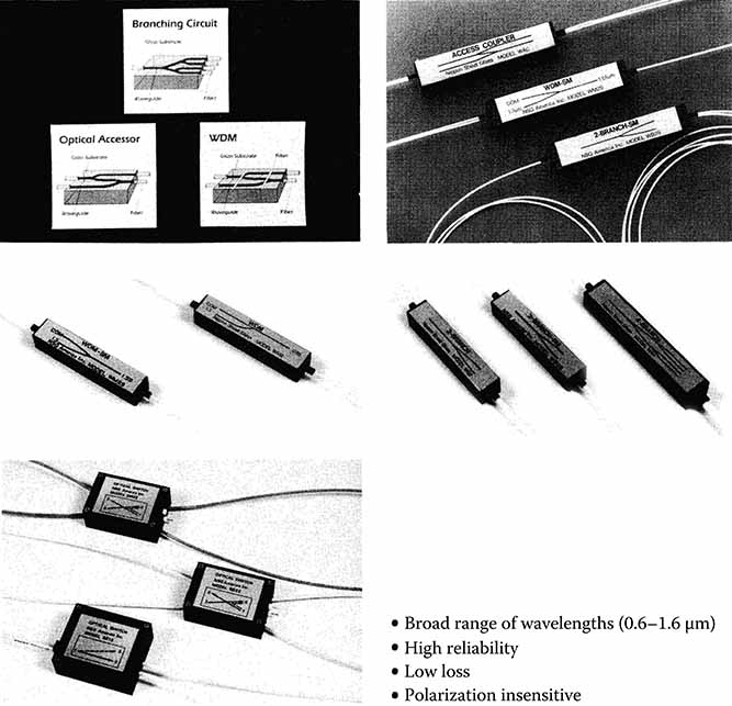
FIGURE 5.39
Ion-exchange borosilicate glass waveguide single mode fiber-optic contents.
The next step in device complexity beyond the splitter is the single mode tree or star coupler. These can be 1 × N, 2 × N, 4 × N, etc. These components usually have equal split ratios but can be manufactured with asymmetric ratios. Dual wavelength devices are more complex and costly. Port counts greater than four usually require splicing of two or more devices and large enclosures or ultimately integration in photonic circuits.
Multimode trees and stars are similar to the single mode devices, but rarely fabricated with asymmetric split ratios. Constructed with fibers from 50/125 to 200/230 μm, they are generally used in high power industrial and medical sensing while the single mode devices are used more in the CATV and DWDM markets. For example, 200/230 devices are used to couple signals from intravenous catheters in arterial blood-gas sensor systems. 100/140 devices are used to link pressure catheters to intracranial pressure monitors. They are also used in rpm monitors for steam turbines.
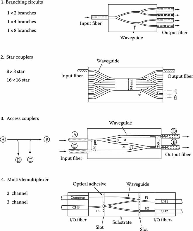
FIGURE 5.40
Applications of graded-index waveguides.
Wavelength division multiplexers/demultiplexers are manufactured using the FBT process for sharp tapers, exploiting interference effects between guided wave devices. These are usually 1310/1550 or 980/1550 devices. Typical isolation in a 1310/1550 device is 20 dB. High isolation devices (>40 dB) can be constructed by splicing two or more devices in series.
Low PDL FBT tap couplers with asymmetric split ratios, typically 1/99 or 5/95, are used in feedback control systems to monitor laser output of sensitive optical instruments where the state of polarization can affect system performance. Low reflection terminations (LRT) are manufactured by creating an asymmetric sphere or fiber loop to prevent reflections from unused splitter ports in bi-directional systems causing unstable laser performance or noise.

FIGURE 5.41
Ion-exchange glass technology for fiber-optic components.
5.12.3 Passive Optical Interconnects
Passive optical components guide, filter, route, adjust and stabilize optical signals transmitted through an optical network. Recent technological advances in the design and production of both passive and active components allow communication equipment suppliers to optimize fiber-optic systems. The ongoing trend is to integrate increasing optical component count into compact modules and custom solutions.
The concept of flexible optical circuits originated at Bell Labs in the late 1980s [104–106]. Originally named “Optiflex” the concept is now produced in similar fashion by nearly a dozen companies including FCI, Polyguide Photonics, Tyco, AIT, Molex, NTT, USConec, and others. Fiber crossovers are designed to minimize stress in the fibers. Several companies manufacture multifiber array connectors suitable for use with the flexible optical routing circuits. These employ precision molded ferrules as well as micromachined silicon v-grooves for accurate alignment of fibers for optimal coupling configurations. Complex fiber management schemes developed at DuPont and later licensed to PolyGuide Photonics, aka Optical Crosslinks Inc., provide the capability to manufacture flexible routing circuits as well as related polymer waveguide based passive components [107].
One key requirement for optical communication systems is the perfect optical shuffle or optical flex board shown in Figure 5.42. Eight sets of eight-input fiber arrays are routed to each of eight sets of eight-fiber output arrays. In other words, one fiber from each of the inputs goes to one fiber of each of the outputs. In Figure 5.42, 1:8 splitters are used to create the eight sets of eight-fiber inputs; and an 8 × 1 switch is used to direct each of the output fibers to a set of single-fiber outputs. While the specific optical wiring may vary from one system application to another the basic optical shuffle component provides the fundamental building block.
This can be accomplished as shown in Figures 5.43 and 5.44, with various fiber routing and packaging schemes. In Figure 5.43, the fibers are ribbonized into 12 sets of 12-fiber arrays, and one fiber from each of the arrays goes to one of the output arrays. The fiber crossovers are housed in a “black box” called the shuffle. A variant of this scheme is shown in Figure 5.44, where the ribbonized fibers enter a sheet of material which contains the routing paths for the fibers which are shuffles as before. The ribbonized fibers are terminated in these examples with optical connectors called the MPO. This approach will work with the variety of mulitfiber connectors available, for example, MTP, MPX, MAC, miniMAC, etc., as the fibers are always ribbonized with 250 μm center-to-center spacing. In the assembly process, standard communication grade optical fiber is laid onto an adhesive substrate material such as Kapton. Following the routing process, a thermoplastic material is laminated over the optical circuit to encapsulate and protect the circuit during handling and environmental extremes.
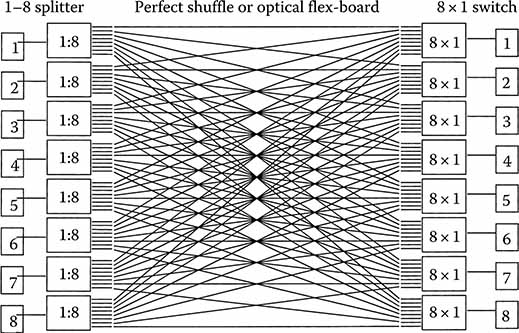
FIGURE 5.42
8 × 8 optical switch component.
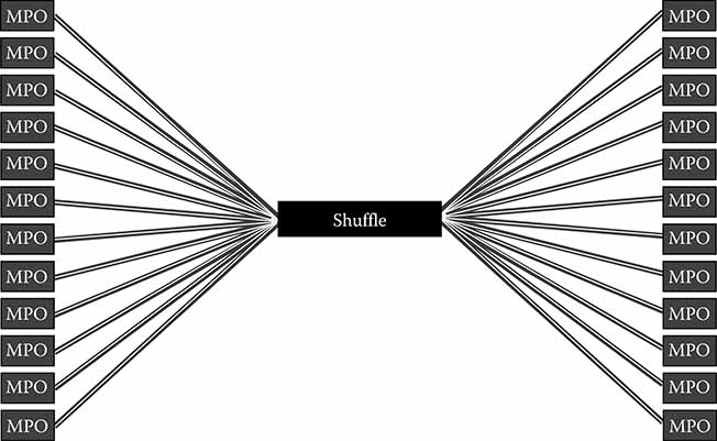
FIGURE 5.43
Optical shuffle.
Another application for optical routing circuits is shown in Figures 5.45 and 5.46. In these cases the optical circuit provides interconnection of optoelectronic components on a circuit card, such as optical transceivers and processors, as well as a connection to the card edge or motherboard, and to a routing cabinet. Other applications include crossovers, splitters, couplers, and multiple simplex or multi-fiber termination points. Routing circuits are tailored for each system application. In most cases the only limitations on the fiber routing paths are the minimum radii of curvature allowable for the individual fibers. Encapsulation protects the fibers from debris, moisture, and handling. This provides maximum flexibility to the equipment system designer.
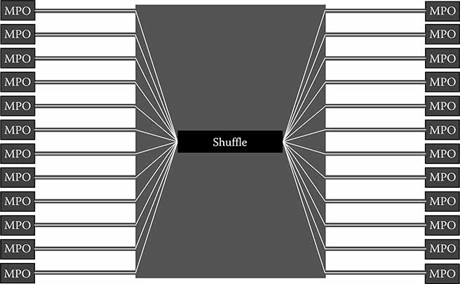
FIGURE 5.44
Optical flex circuit with perfect shuffle function.
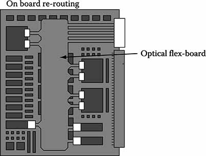
FIGURE 5.45
Optical routing device on circuit board.
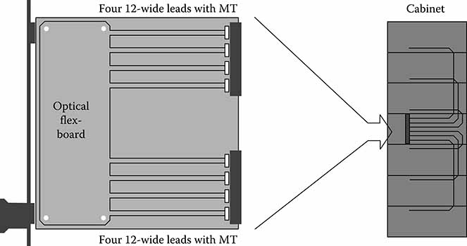
FIGURE 5.46
Optical configuration board.
5.12.4 Configuration of a Curved Transition Waveguide
Intersecting waveguides may be joined either abruptly or smoothly. Abrupt joining is easier from a fabrication standpoint but provides undesirable discontinuities to the traveling waves. The ideal coupling is a curved section, joined tangentially to the end of each individual waveguide. To fabricate such a section, one needs to specify the radius of curvature of this section and one needs to know the location of the center of this curvature relative to some well-established reference point.
Figure 5.47 shows the intersection of waveguides at the Double-Y output. In this case, a single waveguide is split abruptly at point D, into two waveguides which separate at an angle β. This abrupt separation is used so that the angle where the split occurs remains finite. It is desirable to keep this angle small to permit good coupling between the guides. On the other hand, one also desires a larger spread between the guides, in a reasonable distance, than would be attainable with the angle β. So the angle is further increased by the angle γ to a total of α. The following derivation yields the necessary values to locate a curved section of waveguide between points A and B.
The problem can be specified in terms of the angles α and β and the distances a and R. The segment is the distance a between the intersections of the individual guides with the straight output guide (inclined at 0°), and R is the radius of curvature of the connecting section measured from point C. Other angles in the figure are related as follows:
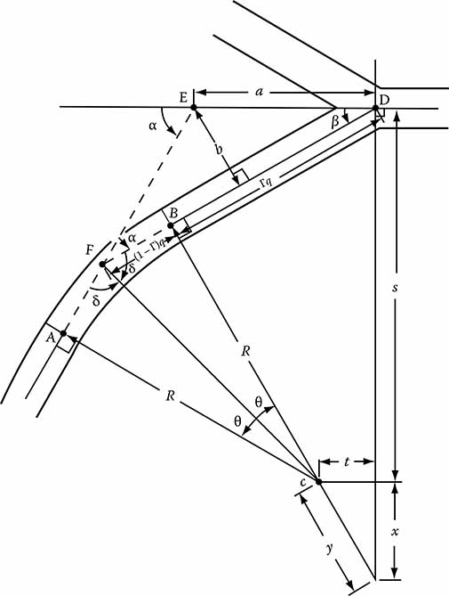
FIGURE 5.47
Geometry of curved transition waveguide.
The distance from the waveguide split to the imaginary intersection of the two angled waveguides, the segment , is defined by
It is seen that point B, the beginning of the curved section, divides q into two sections, and Γ represents the percentage of this division. The radius of curvature is found to be
The center of curvature C is located at distances t and s relative to point D. In order to find t and s we first find x and y
or
and
or
then
or
and
or
A final parameter of interest is the arc length of the curved segment:
In summary, point B, the start of the curved section, is found by starting at point C, going a distance R in the –y-direction, and rotating an angle β. The length of the curve to point A is made by additional rotation of 2θ.
References
1. Hungsperger, R. G. 1984. Integrated Optics: Theory and Technology, 2nd edn. New York: Springer-Verlag.
2. Maractili, E. A. 1969. Dielectric waveguide and directional coupler for integrated optics. Bell System Tech. J. 48(7):2102.
Goell, J. E. 1969. A circular-harmonic computer analysis of rectangular dielectric waveguides. Bell Syst. Tech. J. 48(7):2133–2160.
Schlosser, W. and H. G. Unger. 1966. Partially filled waveguides and surface waveguides of rectangular cross section. Advances in Microwaves. New York: Academic Press, pp. 319–387.
Bartling, J. Q. 1969. Propagation of electromagnetic wave in an infinite rectangular doelectric waveguide. J. Franklin Inst. 287(5):389–407.
Shaw, C. B., B. T. French, and C. Warner III. Further research on optical transmission lines. Scientific Report (2) Contract AF449(638)-1504 AD 625 501. Autonetics Report (C7-929/501), pp. 13–44.
3. Barnoski, M. K., ed. 1974. Introduction to Integrated Optics. New York: Plenum Press, pp. 101–102.
4. Bradley, J. C. and A. L. Kellner. 1983. Multimode structure of diffused slab channel waveguides in uniaxial crystals. SPIE East 83, April, Arlington, VA.
5. Marcatili, E. A. 1969. Dielectric waveguide and directional coupler for integrated optics. BSTI 48(7): 2071–2102.
6. Kuznetsov, M. September 1983. Expressions for the coupling coefficient of a rectangular waveguide directional coupler. Opt. Lett. 8:499 ff.
7. Hutcheson, Lynn. June 1986. Private conversation with author.
8. Mentzer, M. A. 1986. Ion implantation fabrication of gallium arsenide integrated optical components. PhD dissertation, University of Delaware.
9. Mentzer, M. A., R. G. Hunsperger, J. Bartko, J. M. Zavada, and H. A. Jenkinson. 1984. Ion implanted GaAs integrated optics fabrication technology. Proceedings of SPIE 517.
10. Mentzer, M. A., R. G. Hunsperger, S. Sriram, J. Bartko, M. S. Wlodawski, J. M. Zavada, and H. A. Jenkinson. 1985. Ion implanted optical waveguides in gallium arsenide. Opt. Eng. 24:225–229.
11. Boyd, J. T., R. W. Wu, D. E. Zelmon, A. Nauman, and H. A. Timlin. 1984. Planar and channel optical waveguides utilizing silicon technology. Proceedings of SPIE 517.
12. Webb, R. P., and W. J. Devlin. 1986. Resonant semiconductor-laser amplifier as an optically controlled wavelength selector. Conference on Lasers and Electro-Optics, Technical Digest, June, p. 354.
13. Jewell, J. L. 1986. Semiconductor etalons for optical information processing. Conference on Lasers and Electro-Optics, Technical Digest, June.
14. Lee, Y. W., H. M. Gibbs, J. L. Jewell, J. F., Duffy, T. Venkatesan, A. C. Gossard, W. Wiegmann, and J. H. English. 1986. Speed and effectiveness of windowless GaAs etalons as optical logic gates. Conference on Lasers and Electro-Optics, Technical Digest, June.
15. Jewell, J. L., Y. H. Lee, H. M. Gibbs, N. Peyghambarian, A. C. Gossard, and W. Wiegman. 1985. The use of a single nonlinear fabry-perot etalon as optical logic gates. Appl. Phys. Lett. 46:918.
16. Sturge, M. D. 1962. Phys. Rev. 127:763.
17. Stoll, H. A. Yariv, R. G. Hunsperger, and E. Garmire. 1974. Proton-implanted waveguides and integrated optical detectors in GaAs. Digest of Technical Papers. OSA topical meeting on integrated optics, January, New Orleans, LA, pp. 21–23.
18. Tracey, J. C., W. Wiegman, R. Logan, and F. Reinhart. 1973. Three-dimensional light guides in single-crystal GaAs/GaAlAs. Appl. Phys. Lett. 22:10.
19. Tien, P. K. 1971. Lightwaves in thin films and integrated optics. Appl. Opt. 10(11): 2395–2413.
20. Blum, F. A., D. W. Shaw, and W. C. Holton. 1974. Optical striplines for optical integrated circuits in epitaxial GaAs. Appl. Phys. Lett. 25:116.
21. Tien, P. K. Lightwaves in thin films and integrated optics.
22. See, for example, Hunsperger, R. G. 1985. Integrated Optics: Theory and Technology, 2nd edn. Heildelberg: Springer Verlag.
23. Goell, J. E. 1974. Loss mechanisms in dielectric waveguides. Introduction to Integrated Optics, Barnoski, M. K., ed. New York: Plenum.
24. See, for example, 1984. Proceedings of the Second International Conference of Metalorganic Vapor Phase Epitaxy, April, Sheffield, U.K.
25. See, for example, 1986. Abstracts of the Third International Conference on Metalorganic Vapor Phase Epitaxy, April, Universal City, CA.
26. Hutcheson, L. D. 1986. AlGaAs/GaAs processing and growth compatibility for monolithic integration. Proceedings of SPIE 612, January.
27. Chen, T. R., L. C. Chiu, K. L. Yu, U. Koren, A. Hasson, S. Margalit, and A. Yariv. 1982. Low threshold in GaAsP terrace mass transport laser on semi-insulting substrate. Appl. Phys. Lett. 41:1115.
Vawter, G. A., and J. L. Merz. 1984. Design and fabrication of AlGaAs/GaAs phase couplers for OIC applications. Proceedings of SPIE 517, p. 15.
MacDonald, R. I., and D. K. W. Lam. 1985. Optoelectronic switch matrices: recent developments. Opt. Eng. 24:220.
28. Hunsperger, R. G. and M. A. Mentzer. 1989. Optical control of microwave devices—A review. Proceedings of SPIE, September, Boston, MA.
29. Ury, L., K.Y. Lau, N. Barchaim, and A. Yariv. 1982. Very high frequency GaAlAs laser field effect transistor monolithic integrated circuit. Appl. Phys. Lett. 41:126.
30. Matsueda, H. and M. Nakamura. 1984. Monolithic integration of laser diode photomonitor, and electronic circuits on a semi-insumating GaAs substrate. Appl. Opt. 23:779.
31. Dakss, M. L. Kuhn, P. F. Keidrich, and B. A. Scott. 1970. Appl. Phys. Lett. 16:532.
32. Robertson, M. J., S. Ritchie, and P. Dayan. 1985. Semiconductor waveguides: Analysis of coupling between rib waveguides and optical fibers. Proceedings of SPIE 578, p. 184.
33. Hammer, J. M., R. A. Bartolini, A. Miller, and C. C. Neil. 1976. Appl. Phys. Lett. 28:192.
34. Bulmer, C. H., and M. G. Wilson. 1976. Single mode grating coupling. IEEE J. Quant. Electron. QE-14:741.
35. Cherin, A. H. 1983. An Introduction to Optical Fibers. New York: McGraw Hill, pp. 240–241.
36. Hunsperger, R. G., A. Yariv, and A. Lee. 1977. Appl. Opt. 16:1–26.
37. Mergerian, D. and E. C. Malarkey. 1980. Microwave J. 23:37.
Mergerian, D., E. C. Marlarkey, M. A. Mentzer, et al. 1982. Advanced integrated optic RF spectrum analyzer. Proceedings of SPIE 324, p. 149.
Ranganath, T. R. and T. R. Joseph. 1981. Integrated optical circuits for RF spectrum analysis. Final report contract #F33615-78-C-1450. Hughes Research Laboratories for Air Force Wright Aeronautical Laboratories, July.
38. Emkey, W. L. 1983. Optical coupling between single mode semiconductor lasers and strip waveguides. IEEE J. Lightwave Tech. LT-1:436.
39. Kingerly, W. D., Bowen, H. K., and Uhlmann, D. R. 1976. Introduction to Ceramics. New York: John Wiley & Sons, pp. 685–701.
40. Olsen, G. H., and V.S. Ban. 1987. InGaAs: The next generation of photonic materials. Solid State Technol. 30(2):99.
Korotky, S. et al. 1986. Integrated optic narrow line width laser. Appl. Phys. Lett. 49(1).
41. Chung, P. S. December 1986. Integrated electro-optic modulators and switches. J. Electr. Electron. Eng. Aust.—IE Aust. and IREE Aust. 6(4).
42. Kingerly, Bowen, and Uhlmann, Introduction to Ceramics. New York: John Wiley & Sons: 685–701.
43. Boloyaev, R., V. V. Levin, L. E. Marasin, Yu. V. Popov, and L. Yu. Kharberger. 1986. Photorefraction in lithium niobate planar waveguides. Opt. Spectrosc. (USSR) 61(1):119–120.
44. Alferness, R. C. 1986. Titanium diffused lithium niobate planar waveguide devices. ISAF’86 Proceedings, June 8–11.
45. Burns, W., P. Klein, and E. West. 1986. Ti diffusion in Ti:LiNbO3 optical waveguide fabrication. J. Appl. Phys. 60(10).
46. Twigg, M., D. M. Maher, S. Nakahara, T. T. Sheng, and R. J. Holmes. 1987. Study of structural faults in Ti diffused lithium niobate. Appl. Phys. Lett. 50(9):501–503. Bourns, W. et al. 1979. J. Appl. Phys. 50:6175.
47. Caruthers, J., I. Kaminow, and L. Stulz. 1974. Diffusion kinetics and optical waveguiding properties of out-diffused layers in LiNbO3. Appl. Opt. 13(10):2333–2342.
48. Chung. 1986. Integrated electro-optic modulators and switches. J. Electrical Electron. Eng. Bhatt, S., and B. Semwal. 1987. Dielectric and ultrasonic properties of LiNbO3 ceramics. Solid States Ionics 23:77–80.
49. Chung, P. S. Integrated electro-optic modulators and switches.
50. Kingerly, W. D., Bowen, H. K., and Uhlmann, D. R. Introduction to Ceramics. Alferness, R. C. 1986. Optical guided wave devices. Science 234, November 14.
51. Alferness, R. C. Titanium diffused lithium niobate planar waveguide devices.
52. Kingerly, W. D., Bowen, H. K., and Uhlmann, D. R. Introduction to Ceramics.
53. Holman, R., L. Altman-Johnson, and D. Skinner. 1986. The desirability of electro-optic ferroelectric materials for guided wave devices. Proceedings of IEEE CH2358-0/86/0000-0032.
54. MMT Staff Report. October 1987. Direct write lithography: An overview. Microelectronics Manufacturing and Testing 10(11).
Sze, S. M. 1985. Semiconductor Devices Physics and Technology. New York: John Wiley and Sons.
55. Gray, T. September 1986. Thin film deposition technology for hybrid circuits. Hybrid Circuit Technology.
56. Burns, Klein, and West. 1986. Ti diffusion in Ti:LiNbO3 optical waveguide fabrication. J. Appl. Phys. Caruthers, Kaminow, and Stulz. Diffusion kinetics and optical waveguiding.
57. Chung. Integrated electro-optic modulators and switches.
Armenise, Canalia, and DeSario. 1983. Characterization of (Ti0.65Li0.35)O2 com-pound as a source of Ti during TiLiNbO3 optical waveguide fabrication. J. Appl. Phys. 54(1) January.
Twigg, M. et al. Study of structural faults in Ti diffused lithium niobate.
58. Burns, W., P. Klein, and E. West. Ti diffusion in Ti:LiNbO3 optical waveguide fabrication.
Fontaine, M., A. Delage, and D. Landheer. 1986. Modeling of Ti diffusion into LiNbO3 using a depth dependent diffusion coefficient. J. Appl. Phys. 60(7).
Palma, F. and L. Schirone. 1986. Acousto-optic interaction efficiency in Ti:LiNbO3 waveguide collinear Bragg diffraction cell. J. Appl. Phys. 60(10).
59. Alferness. 1986. Optical guided wave devices. Science. 234(4778): 825–829.
60. Twigg, et al. Study of structural faults in Ti diffused lithium niobate.
61. Armenise, Canalia, and DeSario. 1983. Characterization of (Ti0.65 Li0.35)O2 com-pound. J. Appl. Phys. 54(1).
Fontaine, M., A. Delage, and D. Landheer. Modeling of Ti diffusion into LiNbO3. Hickernell, F., S. Joseph, and K. Ruehle. 1986. Surface wave studies of annealed proton exchanged lithium niobate. IEEE Proceedings.
62. Ibid.
Gnauck, A. et al. 1986. Personal discussions with author at Optical Fiber Communication Conference, February, Atlanta, GA.
63. Burns, Klein, and West. Ti diffusion in Ti:LiNbO3 optical waveguide fabrication.
64. Palma, F. and L. Schirone. 1986. Acousto-optic interaction efficiency. J. Appl. Phys. 60(10).
65. Alferness, Titanium diffused lithium niobate waveguide devices.
Armenise, M., C. Canalia, and M. DeSario. Characterization of (Ti0.65 Li0.35)O2 compound.
Fontaine, M., A. Delage, and D. Landheer. Modeling of Ti diffusion into LiNbO3.
66. Twigg, et al. Study of structural faults In Ti diffused lithium niobate.
67. Stallard, W. A., A. R. Beaumont, and R. C. Booth. 1986. Integrated optic devices for coherent transmission. J. Lightwave Tech. LT-4(7).
Armenise, M., C. Canalia, and M. DeSario. Characterization of (Ti0.65 Li0.35)O2 compound.
68. Twigg, et al. Study of structural faults in Ti diffused lithium niobate.
69. Stallard, Beaumont, and Booth. Integrated optic devices.
Alferness. Titanium diffused lithium niobate waveguide devices.
Alferness. Optical guided wave devices.
M. Armenise, C. Canalia, and M. DeSario. 1983. Characterization of TiO2, LiNb3O8 and (Ti0.65Nb0.35)O2 compound growth observed during TiLiNbO3 optical waveguide fabrication. J. Appl. Phys. 54(11).
70. Twigg, et al. Study of structural faults in Ti diffused lithium niobate.
71. Ibid.
72. Stallard, W. A., A. R. Beaumont, and R. C. Booth. Integrated optic devices. Alferness, R. C. Titanium diffused lithium niobate waveguide devices. Alferness, R. C. Optical guided wave devices.
73. Ibid.
Ritchie and Steventon. The potential of semiconductors for optical integrated circuits. British Telecom Research Laboratories, Ipswich, U.K., advance unpublished copy.
74. Eknoyan, O., C. H. Bulmer, R. P. Moeller, W. K. Burns, and K. H. Levin. 1986. Guided wave electro-optic modulators in Ti:LiNbO3 at 2.6 μm. J. Appl. Phys. 59(8):2993–2995.
75. Al-Shukri, et al. 1986. Single mode planar and strip waveguides by proton exchange in lithium tantalate and lithium niobate. Proceedings of SPIE 651.
Glavas, E., P. D. Townsend, G. Droungas, M. Dorey, K. K. Wong, and L. Allen. 1987. Optical damage resistance of ion-implanted LINbO3 waveguides. Electron. Lett. 23(2).
Hickernell, F., S. Joseph, and K. Ruehle. Surface wave studies.
76. Wong, K. K. 1985. An experimental study of dilute melt proton exchange waveguides in X- and Z-cult lithium niobate. GEC J. Res. 3(4).
Jackel, J. L., C.E. Rice, and J.J. Veselka. 1982. Technical Digest (Postdeadline Papers) of Integrated and Guided-Wave Optics. Pacific Grove, CA, PDP1-1.
Nutt, A. C. G., K. K. Wong, D. F. Clark, P. J. R. Laybourn, and R. M. De La Rue. 1983. Proton-exchange lithium niobate slab and stripe waveguides: Characterization and comparisons. Proceedings of Second European Conference on Integrated Optics, 17–18 October.
Wong, K. K., A. C. G. Nutt, D. F. Clark, J.Winfield, P. J. R. Laybourn, and R. M. De La Rue. 1986. Characterization of proton-exchange slab optical waveguides in X-cut LiNbO3. IEEE Proc. J. 133(2).
77. Zang, D. and C. Tsai. 1986. Titanium indiffused proton exchanged waveguide lenses in LiNbO3 for optical image processing. Appl. Opt. 25(14).
78. Zang, D. and C. Tsai. 1986. Single mode waveguide microlenses and micro-lens arrays fabricated in LiNbO3 for optical information processing. Appl. Opt. 25(14).
79. Zang, D. and C. Tsai. Titanium indiffused proton exchanged waveguide lenses.
80. Barnoski, M. K., R. G. Hunsperger, R. G. Wilson, and G. Tangonan. 1975. Proton-implanted GaP optical waveguides. J. Appl. Phys. 44:1925–1926.
Mentzer, M. A., R. G. Hunsperger, S. Sriram, et. al. 1985. Ion implanted optical waveguides in gallium arsenide. Optical Engineering 24 (2) March/April: 25–29.
Mentzer, M. A., R. G. Hunsperger, S. Sriram, J. M. Zavada, H. A. Jenkinson, and T. J. Gavanis. 1983. Temperature processing effects in proton implanted n-type GaAs. Appl. Phys. A32:19–25.
Destefanis, G.L., P. D. Townsend, and J. P. Gailliard. 1978. Optical waveguides in LiNbO3 formed by ion implantation of helium. Appl. Phys. Lett. 32:293–294.
Webb, A. P. and P. D. Townsend. 1976. Refnoindentractive index profiles induced by ion implantation into silica. J. Phys. 9:1343–1354.
Nishimura, T., H. Aritome, K. Masuda, and S. Namba. 1974. Optical waveguides fabricated by B ion implanted fused quartz. Japan. J. Appl. Phys. 13:1317–1318.
Valette, S., G. Labrunie, and J. Lizet. 1975. Optical waveguides in ion implanted ZnTe. J. Appl. Phys. 46:2731–2732.
Valette, S., G. Labrunie, J. Deutsch, and J. Lizet. 1977. Planar optical waveguides achieved by ion implanted in zinc telluride: general characteristics. Appl. Opt. 16:1289–1296.
81. Ziegler, J. F. ed. 1984. Ion Implantation Science and Technology. New York: Academic Press, Inc.
82. Poate, J. M. and J. W. Mayer, eds. 1982. Laser Annealing of Semiconductors. New York: Academic Press.
83. Mentzer, M. A. 1983. Temperature processing effects in proton implanted n-type GaAs. Appl. Phys. A32: 19–25.
Mazey, D. J. and R. S. Nelson. 1969. Radiation Eff. 229.
Gamo, K., T. Inada, J. W. Mayer, F. H. Eisen, and C. G. Rhodes. 1987. Radiation Eff. 33:85.
Williams, J. S. and H. B. Harrison. 1981. Laser and Electron Beam Solid Interactions and Material Processing, J. F. Gibbons, L. D. Hess, and T. W. Sigmon, eds. New York: North-Holland Publishers, p. 209.
84. Williams, J. S. and M. W. Austin. 1980. Appl. Phys. Lett. 36:994.
85. Williams, J. S., M. W. Austin, and H. B. Harrison. 1980. Thin Film Interfaces and Interactions, J. E. E. Baglin and J. M. Poate, eds. Pennington, NJ: Electrochem. Soc., p. 187.
86. Kular, S. S., B. J. Sealy, K. G. Stephens, D. K. Sadana, and G. R. Booker. 1980. Solid-State Electron. 23:831.
87. Eisen, F. H. 1980. Laser and Electron Beam Processing of Materials, C. W. White and P. S. Peercey, eds. New York: Academic Press, p. 309.
Donnelly, J. P. 1981. Nucl. Instrum. Methods 182/183:553.
88. Kacharin, G. A., N. B. Prichadin, and L. S. Smirnow. 1976. Sov. Phys.-Semicond. (Engl. transl.) 9:946.
Golouchenko, J. A. and T. N. C. Venkatesan. 1978. Appl. Phys. Lett. 32:464.
Sealy, J., S. S. Kular, K. G. Stephans, R. Croft, and A. Palmer. 1978. Electron. Lett. 14:820.
Campisano, S. U., I. Catalanmo, G. Fott, E. Rimini, F. Eisen, and M. A. Nicolet. 1978. Solid-State Electron. 21:485.
Barnes, P. A., M. J. Leamy, J. M. Poate, S. D. Ferric, J. S. Williams, and G. K. Celler. 1978. Appl. Phys. Lett. 33:965.
89. Williams, J. S. and M. W. Austin. Appl. Phys. Lett. 36.
90. Gamo, K., T. Ineda, J. W. Mayer, F. H. Eisen, and C. G. Rhodes. 1977. Radiat. Eff. 33:85.
91. Poate, J. M. and J. W. Mayer, eds. 1982. Laser Annealing of Semiconductors. New York: Academic Press.
92. Dupois, R. D. 1984. MOCVD of III-V. Semi conductors. Science 226:623–629.
93. Kallman, W. R. October 1987. MOCVD epitaxy for MMIC program requirements. Monolithic Technology.
94. Dapkus, P. D. 1984. J. Crystal Growth 68:345–355.
95. Fraser, A. and A. Rode. October 1987. Making MMICs with a foundry. Monolithic Technology.
96. Ibid.
97. Parrish, P. October 1987. Computer-aided engineering in GaAs monolithic technology. Monolithic Technology.
98. Damman, C., R. Hulse, and P. Wallace. October 1987. Microwave die sort and wafer mapping for GaAs MMIC manufacturing. Monolithic Technology.
99. Ibid.
100. Fraser, A. and A. Rode. Making MMICs with a foundry.
101. Ho, P., T. Andrade, and E. Johnson. August 1987. GaAs MMIC reliability analysis and its impact on microwave systems, part 1. MSN&CT.
102. U.S. Government Printing Office. October 1986. Military Handbook, Reliability Prediction of Electronic Equipment, MIL-HDBK-217E.
103. Fraser, A. and A. Rode. Making MMICSs with a foundry.
104. Holland, W. R., J. J. Burack, and R. P. Stawicki. 1993. Optical fiber circuits. Proceedings of 43rd ECTC (IEEE), June.
105. Nordin, R. A., W. R. Holland, and M. A. Shahid. 1995. Advanced optical interconnection technology in switching equipment. J. Lightwave Technol. 13(6).
106. Grimes, G. J. et al. 1993. Packaging of optoelectronics and passive optics in a high capacity transmission terminal. Proceedings of 43rd ECTC (IEEE), June.
107. Booth, B. Optical Crosslinks, Inc. 2002. Private conversation with author.