
3
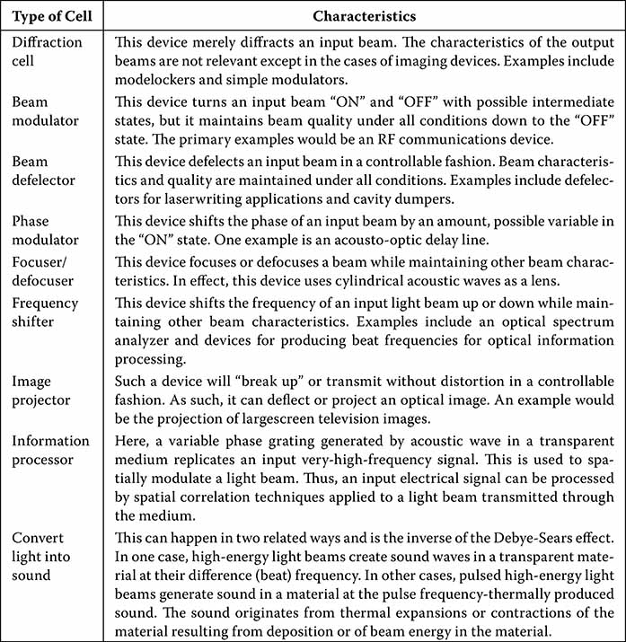
Acousto-Optics, Optical Computing, and Signal Processing
We first address the acousto-optic (AO) effect called Bragg diffraction, utilized in devices called Bragg cells. The basic operating principles of Bragg cells, the components, the applications, and the performance of some systems developed using Bragg cells will be discussed. The implementations of the AO effect are widespread. Much research continues due to the potential for great speeds and small size of optical processing devices. AO Bragg cell signal processing is an analog technology showing great promise, in an age where digital electronics is most emphasized.
3.1 Principle of Operation
Acousto-optics deals with the interaction of sound and light. In Bragg cells, the AO interaction takes place in media such as silicon, lithium niobate, tellurium dioxide, or even glasses. Figure 3.1 shows a basic Bragg cell [1]. As light enters from the left, it is interfered with by the upwardly propagating longitudinal sound waves. The sound waves are introduced by a piezoelectric transducer, which is vibrating at an RF frequency of 100 MHz to over 10 GHz. (This is the range of Bragg cell technology and not of any single Bragg cell device. Bandwidth considerations will be covered later.) The vibrations set up minute changes in the AO material’s index of refraction via the photoelastic effect which creates a diffraction grating [2]. When light travels across the grating, assuming certain angular conditions, it is diffracted at an angle proportional to the RF frequency of vibration.
The angular condition is called the Bragg angle and is given by [3]
sinαB=λ2Λ(3.1)
where
λ is the wavelength of the light in the acoustic medium
Λ is the acoustic wavelength
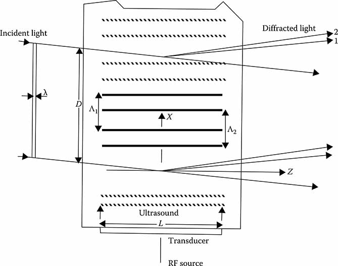
FIGURE 3.1
Bragg cell diffraction.
Note that the Bragg angle depends on the acoustic wavelength. The actual mechanism of AO diffraction is explained by a momentum diagram in Figure 3.2 [4]. The vector sum is
kd=ki+ka(3.2)
where
ka is the acoustic wave vector
ki is the incident wave vector
kd is the diffracted wave vector
When the light beam enters the Bragg cell at the Bragg angle, the diffracted beam exits at the vector sum of the incident light and the acoustic wavefront. Each diffracted beam is Doppler shifted from the incident beam by the diffracting acoustic frequency. If the acoustic wavefront is composed of more than one different frequency, then the optical output will be a diffracted light beam corresponding to each input frequency. The RF frequency(s) at the transducer controls the angle at which the light beam(s) exits the Bragg cell. The properties of the Bragg cell have spurned much effort in the research and development of compact RF spectrum analyzers as well as Bragg cell correlators and convolvers for radar signal processing that are smaller and lighter than their digital VLSE and RF electronic counterparts.
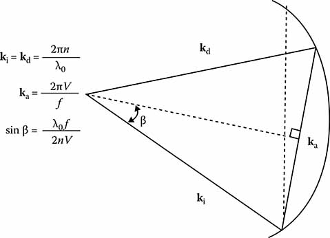
FIGURE 3.2
Wave vector diagram for AO diffraction.
3.2 Basic Bragg Cell Spectrum Analyzer
The components of a Bragg cell receiver are shown in Figure 3.3 [5]. The light source is a laser for optimum performance. The beam expander, or collimator, evenly distributes the light along the acoustic wavefront (top to bottom in Figure 3.3) to match the interaction aperture of the Bragg cell. After light is diffracted into the RF signal components a lens, called the Fourier Transform lens, focuses the light beams into a photodetector (PD) array that is mounted at the lens focal point. Each pixel of the PD array corresponds to a small frequency band, the sum of which makes up the entire bandwidth of the Bragg cell. The minimum frequency difference of two RF signals that are resolvable is approximately equal to 1/τ, where τ is the acoustic transit time across the interaction aperture.
The time bandwidth of the Bragg cell, N = τΔf, where Δf is the bandwidth of the Bragg cell, theoretically provides the total number of signals that can be simultaneously resolved by the Bragg cell receiver [6]. One virtue of an AO material is the high time bandwidth product. Figure 3.4a shows bandwidth-resolution contours for some materials [7]. The frequency bandwidth is the vertical axis, and the time delay is the horizontal axis. The time delay relates to the frequency resolution by Δf = k/T, where T is in μs, f in KHz, and k is a constant of value of 1.2–2.0. If the bandwidth is read on the vertical axis, and the time delay on the horizontal axis, the maximum time bandwidth product of the Bragg cell can be determined. The low frequency time bandwidth product is limited by the size of the crystal that governs the acoustic wave’s transit time.
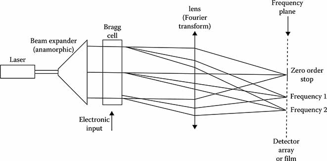
FIGURE 3.3
Basic AO spectrum analyzer.
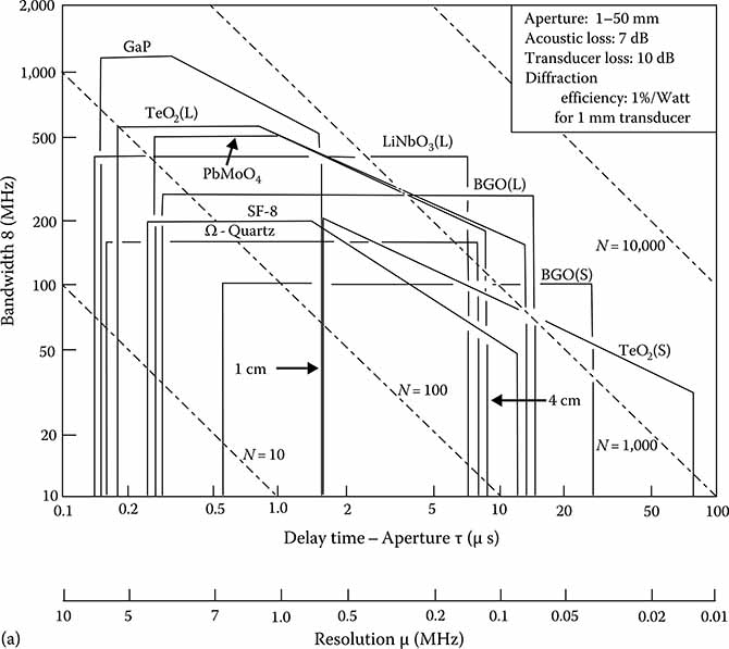
FIGURE 3.4
(a) Bandwidth-resolution contours. (b) Types of AO devices.
The high frequency time bandwidth product is limited by the acoustic loss of the crystal. There are other parameters that govern the choice of materials, and they will be introduced later.
Some of the uses of the Bragg cell are shown in Figure 3.4b [8]. We will concentrate here on the Bragg cell receiver, especially the integrated optic Bragg cell receiver, where the beam collimator, the Bragg cell, and the Fourier Transform lens are formed on the same substrate. Figure 3.5 shows the basic IO Bragg Cell receiver [9].
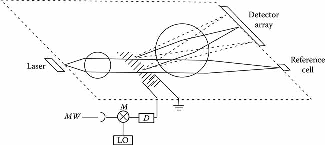
FIGURE 3.5
Integrated optic spectrum analyzer schematic.
3.2.1 Components of Bragg Cell Receivers: Light Sources
The light source is a key component in the Bragg cell receiver.
The Bragg receiver requires a collimated, monochromatic (coherent), low-noise source for optimum performance. In the optical processor, the light source is like a local oscillator in superheterodyne receiver. Noise on the oscillator will be transferred to the output. Helium-Neon (HeNe) lasers are ideally suited for this application, possess narrow spectral bandwidths, and have demonstrated lifetimes over 10,000 hours. LED’s can be used as sources in incoherent optical processors, but are not suitable for the simple Bragg cell receiver, because of their broad spectral emission. Semiconductor lasers have spectral bandwidths narrower than most LED’s but not as narrow as a HeNe laser. For applications where high resolution is not required, semiconductor lasers may even improve performance because of their high output power with a much smaller size and lower power consumption. [10]
For some materials such as LiNbO3, the AO diffraction efficiency using an 850 nm source can be reduced to 50% of the efficiency using a 633 nm source [11]. The higher output power of the semiconductor laser offsets this. While the choice of the source depends upon the application, for the ultimate in performance, where size and power consumption are less important, the HeNe laser is used. Where miniaturization and power consumption are most important, the semiconductor laser is the best choice. The semiconductor laser must be butt coupled to the edge of the IO Bragg cell. Materials that make a good laser, such as AlGaAs, do not possess good AO properties, and the good AO materials, such as LiNbO3, cannot be made into lasers.
3.2.2 Lenses
The lenses in an IO Bragg cell are waveguide lenses. Various types of waveguide lenses have been devised, four of which are illustrated in Figure 3.6 [12]. The same effect as conventional lenses is created with step increases in thickness. A dome-shaped thickness increase is a Luneburg lens; and the inverse, a dome-shaped depression, is basically a geodesic lens. The geodesic lens is the most highly developed, because it is easier to grind the waveguide to near spherical depression than to add material to create a dome. Holographic lenses can be produced by creating grating structures with varying periodicity. The geodesic lens functions using the geometrically longer paths of rays in the center portion relative to the edges. Two lenses are used in the Bragg cell receiver—one between the light source and the cell and the other between the cell and the photodiode array.
The beam collimator determines the interaction aperture of the acoustic wavefront. The wider the aperture, the more frequency resolution is possible, to a point. The acoustic attenuation of various materials limits the aperture size.
Several mechanisms are thought to be responsible for acoustic attenuation. In many materials, Akheiser loss caused by thermal relaxation is the dominant mechanism. For these materials, the attenuation (in dB per unit length) will increase as the square of the frequency. Other acoustic modes exhibit frequency dependencies that range from linear to square. For these materials, other mechanisms such as scattering from lattice imperfections are important in the attenuation process. The acoustic attenuation measured for certain acoustic modes tends to vary widely from sample to sample, even for pieces cut from the same crystal boule. This indicates that lattice dislocations and foreign particle impurities are dominant in the attenuation process. While measures of these crystal imperfections such as etch pit density have been correlated to optical and electrical crystal properties, these measures have not been applied in acoustic attenuation studies. [13]
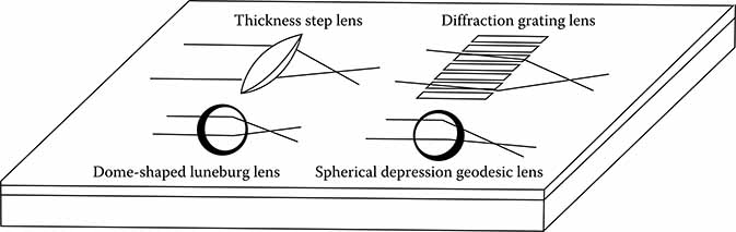
FIGURE 3.6
Four implementations of optical waveguide lenses.
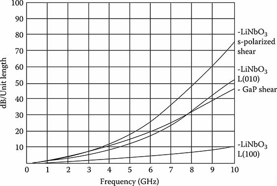
FIGURE 3.7
Acoustic attenuation in various low-attenuation AO materials.
Figure 3.7 compares several acoustic modes which exhibit low acoustic attenuation [14].
3.3 Integrated Optical Bragg Devices
Bragg cell diffraction will now be described more thoroughly. The Bragg cell diffraction efficiency (in percentage of input light deflected per watt of input RF power) is given by [15]
η=π22λ30M3(f0τ)12(lh)(3.3)
where
λ0 is the optical wavelength
f0 is the center frequency of operation
τ is the AO time aperture
M3 is the material figure of merit
l is the normalized electrode length (and the AO interaction length)
h is the normalized electrode height
The efficiency is stated in percentage per Watt of RF drive. Typical bulk diffraction efficiencies are 29%/W at 1.1 GHz, and 105%/W at 350 MHz, both for GaP cells.
SAW diffraction efficiencies are higher, such as 200%/W around 600 MHz, but the optical losses are higher. Equation 3.3 assumes the piezoelectric transducer is of the interdigital type that emits surface acoustic waves. The interdigital elements couple the electric excitation field directly onto a piezoelectric material. The elements are metal-deposited onto the AO material.
The light at the output of a Bragg cell is not entirely diffracted. For example, using a typical RF input power of 100 mW and the 200%/W SAW diffraction efficiency mentioned previously, the diffracted light would be 200%/W × 0.1 W = 20%, with 80% of the light undiffracted (or zeroth order). The desired light output is either of order 1, in the case of upward Doppler shifting, or −1, for downward Doppler shifting. A PD is usually put at the zeroth order focal point, after the Fourier Transform lens, to absorb energy and to act as a built-in test device for monitoring the laser output.
Referring back to Equation 3.3, it is obvious that the Bragg angle changes with the RF operating frequency. In early receiver designs, the Bragg angle was optimized for the center frequency, but the Bragg cell became very inefficient as the input frequency moved away from the center. The bandwidth of the Bragg cell is determined by the acoustic radiation pattern of the transducers. The bandwidths of modern receivers approach an octave, so there are several things that can be done to maintain good AO efficiency over a wider bandwidth. The interaction length can be decreased, but the AO efficiency also drops. More commonly, the transducers are designed as a phased array, with each element staggered forward as the light travels across the Bragg cell. Figure 3.8 illustrates this [16]. This works quite well with IO Bragg cells, especially those made with LiNbO3, which is a strong piezoelectric material. The interdigital elements can easily be deposited directly onto the substrate. Another approach is the stagger-tilted array, where each element is tilted slightly to be optimized for its segment of the system bandwidth [17]. Figure 3.9 illustrates this method. The electrical impedance of a typical transducer array is about 9 Ω. The impedance of the driving electronics is 50 Ω, so there must be an impedance-matching transformer of some kind at the transducer interface.
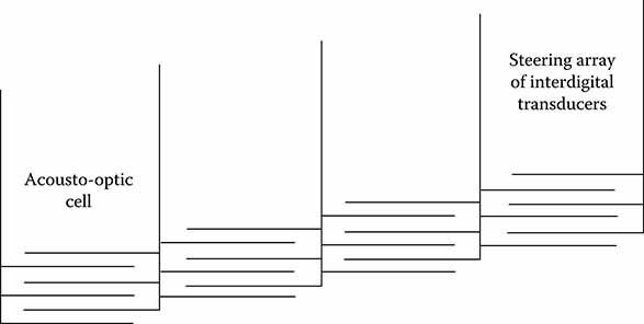
FIGURE 3.8
Staggered transducer array.
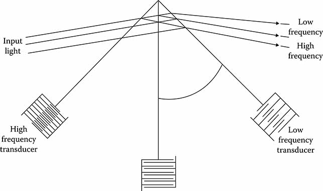
FIGURE 3.9
Angular staggered-tilted transducer array.
3.3.1 Fourier Transform, Fourier Transform Lens
The function of the Fourier Transform lens is to rearrange the diffracted light beam output from frequency-dependent Bragg angles to frequency-dependent positions, so that the output of the PD array is a linear distribution of frequencies. The light output, or what the PDs see is three sinc functions [18]:
u(xf)=k[sinclxfλF+m2sincl((xfλF-f)+m2sincl(xfλF+f))](3.4)
where
xf is the position of the spot
l is the AO aperture
m is the grating modulation depth or RF signal level
f is the reciprocal of the diffraction grating spacing or 1/Λ
k is a constant that accounts for the laser light output and the system’s optical losses
F is the distance between the lens and the focal plane or PD array
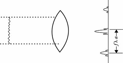
FIGURE 3.10
Fourier transform of a rectangular window with sinusoidal grating.
The first term is the zeroth order term which is not dependent on the RF input, and the last two terms are the first order terms, the “−f” term being the downward Doppler shift, and the “+f” term the upward shift. Figure 3.10 is an illustration of this.
3.3.2 Dynamic Range
The light intensity on the PD array is proportional to the square of the intensity:
l(xf)=|U(xf)|2(3.5)
This illustrates Bragg cell technology’s weakness: dynamic range. For example, for a Bragg cell receiver to have 60 dB of RF dynamic range, the PD array must have 120 dB. Dynamic range will be referred to with the RF signal as the reference. One hundred and twenty decibel (60 dB RF) is beyond the performance for most PDs. The PD limits the RF dynamic range of the system to between 25 and 40 dB, depending on the type of PD used, but the Bragg cell itself has a dynamic range between 50 and 70 dB [19].
The two categories of linear array PDs useful for AO signal processing are the photodiode and the MOS depletion mode sensor [20].
One example of a commercially available randomly addressable photodiode linear array is the Reticon CP1006 device. It consists of two interdigitated rows of 256 photodiodes with a width of 50 μm. Its dynamic range is 20 dB for noncoherent (conventional) detection processors. Another commercially available array is the Reticon CP1023 device, with CCD shift registers. It has 256 elements on an 18 μm pitch, with four independent outputs of 64 elements each, capable of a 6 MHz data rate (10.6 μs access time). Its specified dynamic range is 30 dB for noncoherent detection systems. A detector that has been built for AO Braggs cell receivers has 140 elements on a 12 μm pitch, including an element for zeroth order dumping. The measured dynamic range is 41 dB for 2 μs access time. A MOS-CCD PD has been built to be used with an IO Bragg cell receiver with four groups of 25 elements each. It is designed to be read out in four parallel channels, or two parallel channels of 50 elements.
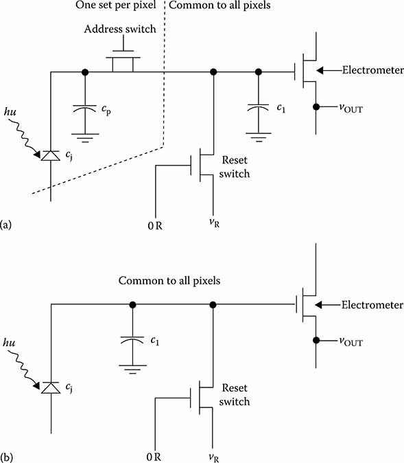
FIGURE 3.11
Schematic representation of photodiodes and CCD arrays: (a) photodiode read-out circuit; (b) CCD read-out circuit.
No dynamic range data was given. Both types of PDs are shown in Figure 3.11 [21].
3.4 Noise Characterization of Photodetectors
As detailed in the Borsuk reference [22], “the linear dynamic range of PDs for AO signal processing can be expressed as the ratio of the maximum charge capacity of the diode-capacitor combination (pel) to the rms number of noise electrons, both expressed here in units of charge:
DDET=QT[ˉQ2T(NES)]12(3.6)
where
QT is the charge capacity of a pel
NES is the noise equivalent signal
The relationship between system dynamic range and sensor dynamic range is
DSYSTEM≤KDDET(3.7)
where K is a function related to the system transfer function. The inequality indicates that the system dynamic range may be limited by the detector. The NES is defined as the input exposure density, E (NES), which will make the SNR equal to unity at the sensor output:
E(NES)=[ˉQ2T(NES)]12RDΛ(μJm2)(3.8)
where
[ˉQ2T(NES)]12
RDΛ is the pel responsivity given by
RDΛ=ARλ=AqnHv(3.9)
where
H is Plank’s constant
v is the optical frequency
q is the electronic charge
A is the active area of a pel
n is the total quantum efficiency
The NES is separable into two components: temporal noise and fixed pattern noise. This separation can be expressed in terms of rms noise electrons by the expression
[ˉQ2T(NES)]12=[ˉQ2tempora1+ˉQ2spatia1]12(3.10)
A summary of these noise sources is presented in the following table for MOS CCDs and photodiode arrays. The choice between selecting a photodiode and CCD for a given AO system application is dependent principally upon trade-offs between speed of operation, sensitivity, and dynamic range. In general, for low temporal noise performance (QT(NES)/q < 200 e−) and moderate dynamic range (102), CCDs are superior to photodiode arrays principally because of the low output sensing capacitance at the electrometer as opposed to the photodiode capacitance. On the other hand, for high clock rates (≥5 MHz), sensitivity is principally limited to amplifier noise common to both CCDs and photodiode arrays to about 500–1000 e−, making the higher dynamic range (105) obtainable with photodiodes attractive.” The PD-capacitor combination responds to optical energy, so the PD response to short duration pulses, especially those that are shorter than its integration time, is a function of the pulse width. It τ is the RF ultrasonic propagation time across the Bragg cell, Ts is the integration time, and PW is the input signal pulse width, then there are three signal conditions [23]:
| CCD | Photodiode | |
| Intrinsic | Bulk traps | Leakage |
| Leakage | Photon shot | |
| Photon shot | ||
| Circuit | Transfer inefficiency (kT/C)1/2 Johnson–Nyquist in output reset operation | (kT/C)1/2 Johnson–Nyquist in diode reset operation |
MOS electrometer Signal proc. Amp Fixed pattern A/D quantizing noise |
||
PW>Ts,τ<PW<Ts,PW<Ts(3.11)
A graph of PW versus dynamic range is shown in Figure 3.12.
3.5 Dynamic Range Enhancement
Several optoelectronic techniques exist to extend the dynamic range of the PD. One technique utilizes two linear PD arrays and a beam splitter. Light intensity is divided unequally between the two detectors. After the photodetector which receives the majority of the light intensity saturates, the second detector array output is utilized. In this way the dynamic range of the two detector arrays can be combined to yield a total detection range which is the sum of the dynamic range of the PD arrays [24].
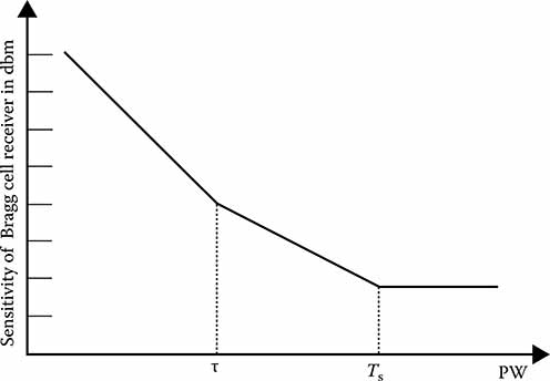
FIGURE 3.12
Sensitivity of Bragg cell receiver versus pulse width.
Another dynamic range enhancement technique uses a Mach–Zehnder interferometer (MZI) system. This approach is illustrated in Figure 3.13.
The optical beam is split between two Bragg cells. The first of these is driven by the signals to be analyzed. The second is driven by a local oscillator reference waveform producing diffracted output reference beams which are recombined with the diffracted signal beams and then focused on the PD array. The beam recombiner is arranged to angularly shift the diffracted reference beams by a small amount so that the resultant interferometric mixing produces output signals at some intermediate frequency IF which is the same for all PD’s. The heterodyned output signals are then bandpass filtered to provide immunity against DC light levels and improve discrimination against detection channels. As the PD heterodyne signal power is now proportional to the RF signal input power, the dynamic range is greatly improved [25].
This technique was accomplished using bulk techniques and has yet to be implemented using IO techniques.
3.6 Photodetector Readout Techniques
Information readout schemes embrace several different parameters. These include PD integration time, number of PDs, and pel access time. The access time and the integration time are usually matched, but a compromise must be reached in dealing with the number of PDs and their access/integration time. It is desirable to have many PDs, but it is also desirable to access them often to detect short pulses, and to most accurately determine time-of-arrival (TOA) information in ECM applications.
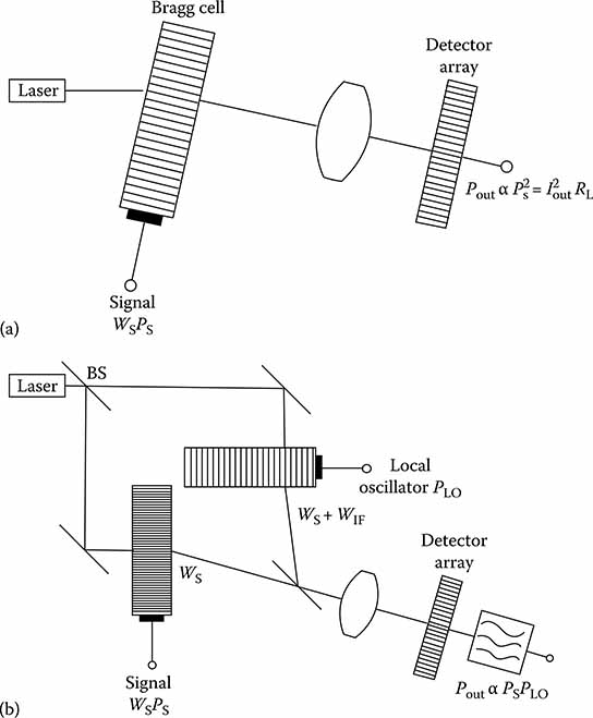
FIGURE 3.13
(a) Conventional power spectrum analyzer. (b) Interferometric spectrum analyzer.
For example, to achieve a 0.5 μs TOA resolution in a 1 GHz wide receiver with 1 MHz resolution (1000 PDs), a PD must be accessed every 0.5 ns. GaAs CCDs have been built that contain much of the readout circuitry on the same die (called self-scanning), but at speeds of 500 MHz, or every 2 ns [26]. Faster speed devices are in development. An alternative approach to accessing many PDs quickly is to arrange them in series–parallel readout schemes with two, four, or more PDs accessed simultaneously. More sophisticated postprocessing techniques are required, but the faster access time is worth the hardware cost if access speeds are important.
3.7 Bulk versus Integrated Optic Bragg Cells
Bulk type Bragg cell receivers now have the edge on dynamic range, bandwidth of operation, high center frequency, and frequency resolution. This is because every component of the system can be separately optimized, and the light propagates through air from component to component. IO type Bragg cells cannot have every component optimized, and compromises must be made to integrate the system. For example, the geodesic lens focuses fairly well, but a precision-ground conventional lens focuses more sharply. In IO systems, the light is coupled into a waveguide, processed, and coupled out to the PD array. The light is subject to waveguide losses of 0.5–1.0 dB cm−1, coupling losses of 3 dB per coupling, and scattering caused by impurities in the waveguide. Scattering causes the PD array to have a higher background noise in frequency-adjacent pels, degrading the resolution. One advantage of IO Bragg cells is their mechanical stability and ruggedness. Everything moves together, eliminating any microphonic interference. This makes IO receivers desirable for avionic and other size-and –weight-constraint applications.
3.8 Integrated Optic Receiver Performance
Two IO Bragg cell receivers that have been developed will be discussed. The first was proposed in 1977 by Hamilton et al. [27] and in 1978 by Barnoski et al. [28]. It includes a semiconductor laser, a Y-cut LiNbO3 substrate with indiffused Ti to form the waveguide, geodesic lenses, interdigital SAW transducers, and a CCD PD array coupled at the output. Design parameters were presented for a 400–800 MHz spectrum analyzer with a projected resolution of 4 MHz, and 40 dB dynamic range.
This was in response to a number of devices and system objectives. First was to identify the amplitude and frequency of emitters and to separate the different emitter categories, such as narrow pulse, wide pulse, and CW. Signals that met a specified detection criterion were to be sorted to allow reduction in data handling, while maintaining a minimum intercept uncertainty time constant. The device objectives were a monolithic integrated circuit which could interface to external systems, which operated with low noise and at high speed and low power consumption.
The first receiver built and demonstrated was by D. Mergerian et al. at Westinghouse (see Figure 3.14) [29]. A 100 μW HeNe laser was end-fire coupled into an x-cut LiNbO3 crystal indiffused with Ti to 280 Å for a waveguide, and a 140 pel self-scanned photodiode array butt coupled at a 45° angle to the waveguide at the other end. Geodesic lenses were formed by single-point diamond turning to >0.5 μm tolerances. The lenses had an insertion loss of about 2 dB. With >5% of the input light diffracted by the SAW’s, the measured dynamic range was around 40 dB. A 400 MHz bandwidth centered at 600 MHz was scanned by dividing the 140 pels into 20 groups of 7 each. A resolution of 4 MHz was achieved. The clock rate was 5 MHz, providing simultaneous pulse detection for 0.3–3.0 μs pulses separated in frequency by 20 MHz. The maximum RF power fed into the transducers was 60 mW. It is interesting to point out that the HeNe laser, emitting 100 μW, is near the power threshold of optical damage in LiNbO3. The authors pointed out that performance could be greatly enhanced by using a longer wavelength semiconductor laser, due to the increasing damage threshold with increasing wavelength in LiNbO3. For comparison, bulk-type receivers have been built with 1 GHz of bandwidth, 1MHz of resolution, and 40 dB of dynamic range; however, wider bandwidth can potentially be achieved with the integrated optical spectrum analyzer using multiple arrays of tilted transducers or chirped transducers.
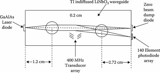
FIGURE 3.14
Westinghouse design for advanced IOSA.
3.9 Nonreceiver Integrated Optic Bragg Cell Applications
Other applications of AO Bragg cells must be split into 1-D and 2-D cases, because IO implementations can only be 1-D. Only those systems realizable in IO technology will be mentioned. The space-integrating and the time-integrating correlators are shown in Figures 3.15a and b, respectively. These are 1-D devices. In the space-integrating correlator, “the received signal g(t) is fed into the Bragg cell at P1, which is illuminated at the correct angle. Lenses L1 and L2 image plane P1a onto plane P1b. A slit filter at P2 performs the necessary single-sideband modulation of the data” [30] by rejecting the zeroth- and the undesired first-order modes.
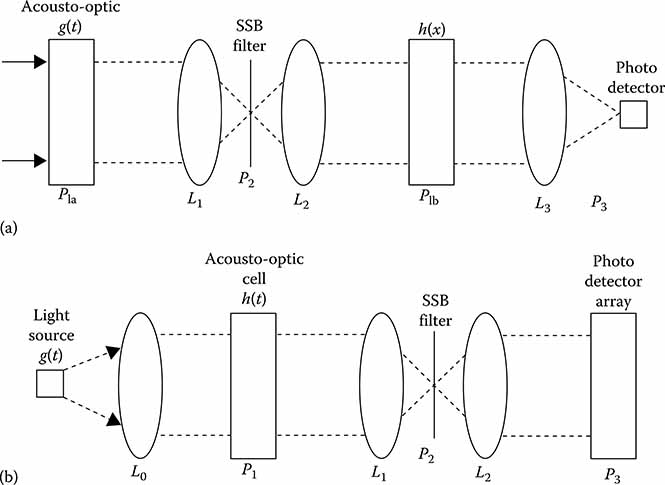
FIGURE 3.15
(a) Space-integrating AO correlators. (b) Time-integrating AO correlators.
The signal incident with P1b is g(x − vt) = g(t − τ). Since τ is proportional to t, which will be the output variable, this substitution is allowable. Thus, incident on P1B is a wavefront proportional to the complex-valued signal g(x − τ). Stored on a mask at P1b is the reference transmitted signal code h(x). The light distribution leaving P1b is thus h(x) = g(t − τ). The Fourier Transform of this signal is formed by L3 at the output plane, where we find
U2(u,t)=∫g(x-τ)h(x)e(-j2τux)dx(3.12)
When evaluated by an on-axis PD at P3, Equation 3.12 becomes
U2(t)=∫h(x)g(x-τ)dx=h⊗g(3.13)
or the correlation of g and h. The integration of Equation 3.13 is performed over distance x. The output correlation variable is time, since the time output from the simple on-axis PD is the correlation pattern. Hence, the name space-integrating correlator is given to this architecture [31].
Figure 3.15b shows the time-integrating system. “Here the integration is performed in time (rather than space) on the output detector. The output correlation appears as a function of distance across the output detector array. An input light source such as an LED or a laser can be modulated with the received signal g(t). Lens L1 collimates the output, and an AO cell at P1 is uniformly illuminated with the time-varying light distribution g(t). The transmittance of the cell is now described by h(t − τ), where again τ = x/v. The light distribution leaving the cell is g(t)h(t − τ). Lenses L1 and L2 image P1 onto P3 (with SSB filtering performed at P2), where time integration on a linear PD array occurs. The P3 light distribution (after time integration occurs on the detector) is thus
U3(x)=∫h(t-τ)g(t-τ)dt=g⊗h(3.14)
or again the correlation of the received and reference signals. In this case, the integration is performed in time and the correlation is displayed in space.
The optical correlators of Figures 3.15a and b employ 1-D devices and simple imaging lenses and are relatively easy to implement. They realize the correlation operation with a moving-window transducer without the need for a matched spatial filter as in conventional correlation optical processors with fixed-format transducers. The space-integrating system can accommodate large range-delay searches between the received and reference signals; however, the signal integration time and time-bandwidth product that this system can handle are small, limited by the aperture (40 μs dwell time is typical) and TBWP (1000 is typical) of the AO cell.
In the time-integrating system, the signals must be time aligned, and only a much smaller range-delay search window (equal to 40 μs typical aperture time of the cell) is possible; however, the time-integrating processor allows longer integration time (limited by the integration time and noise level of the detector) and the associated correlation of longer TBWP signals” [32].
3.10 Optical Logic Gates
The AO signal processing systems discussed previously may be considered representative of the traditional analog optical computing technology. Technological niches for analog optical computing include image enhancement and noise reduction, spectrum analysis of RF signals, pattern recognition, and signal correlation in radar, sonar, and guidance systems. Another class of devices is directed toward the development of digital optical computer systems. Combinations of only 10–20 of these gates could potentially improve a hybrid opto-electronic processor speed by a factor of 100–1000. The following examples are representative of this emerging device technology.
3.10.1 Introduction
All optical signal processing systems for both optical communications and optical computing have tremendous potential for dramatically improving the information handling capacity and data rate in various signal processing systems by keeping the information in optical form during most of the processing path [33]. Major improvements in real-time signal analysis can be obtained through the implementation of all-optical circuits due to the advantage of low power consumption, high speed, and noise immunity. Additionally, all optical systems lend themselves directly to implementation in highly parallel, high throughput architectures.
Dynamic nonlinear optical processes lie at the heart of these optical logic devices. The index of refraction of a semiconductor can be significantly varied through the creation of electrons, holes, and excitons or by exposure to high intensities of light. Changes in these properties can induce absorptive or dispersive bistability in the semiconductor system [34]. A system is said to be optically bistable if it has two output states for the same value of the input over some range of input values. Relaxation properties of the excited semiconductor state dictate the characteristics of these optically induced optical changes.
Gibbs et al. [35] in 1979 were among the first to apply excitonic effects to optical bistability in GaAs. Bistability was demonstrated just below the exciton resonance in a cryogenically cooled, 4 μm thick, GaAs sample utilizing approximately 200 mW of optical power. The device exhibited a switch-off time of approximately 40 ns. This bistability was due to the change in refractive index resulting from nonlinear absorption in the vicinity of the exciton resonance. One limitation to further progress in this area was that excitonic resonances are generally not seen in room-temperature direct-gap semiconductors due to temperature broadening effects.
It has been found, however, that multiple quantum well (MQW) structures show strong exciton resonances at room temperature due to the QW confinement and consequential increase in binding energy of the excitons [36]. These resonances show saturation behavior similar to that observed at low temperature in conventional semiconductors. As such, the MQW structure represents a preeminent class of device to be researched for implementation in optical logic function units.
Bulk and integrated bistable devices have demonstrated the ability to perform a number of logic functions [37]; however, various device parameters such as the physical size, power requirements, and speed and temperature of operation have generally proved to be impractical. Two devices that show promise as optical processing components are the Double-Y Mach–Zehnder Interferometric Optical Logic Gate (Double-Y) and the MQW Oscillator.
3.10.2 Interferometer and Quantum Well Devices
Individual MZIs have been demonstrated in various materials and have been used as modulators and switches [38]. The MQW Oscillator makes use of the nonlinear optical effects unique to the MQW structure. Both the Double-Y, which is an extension of the MZI concept, and the MQWO devices lend themselves directly to fabrication in GaAs material. Both devices can overcome the limitations of speed and operational temperature mentioned previously. In its present configuration, the Double-Y is about 2 cm long and requires rather large optical powers for switching. On the other hand, the MQW is already a small, low-power device.
The Double-Y and MQW oscillator devices utilize a total of three optical effects to perform their logic and switching functions. These are the linear electro-optic, or Pockels effect, the nonlinear index of refraction, and the Quantum Confined Stark Effect (QCSE). Derivations of the first two effects are included at the end of Chapter 2. The Double-Y device has been studied and fabricated in LiNbO3 [39] and in AlGaAs [40]. The MQW Oscillator can be implemented in several forms, one of which has been studied by Wood et al. [41].
A schematic diagram of the Double-Y device is shown in Figure 3.16. The signal of interest is input at the center or control leg. The signal splits at the Y and then recombines. The output depends on how this signal recombines. If the path lengths down the two legs are identical (or differ by an integral number of wavelengths) then the control signal recombines in phase and is referred to as a “one.” If the path lengths differ by an integral number of half wavelengths, the signal recombines destructively, resulting in a “zero” output.
The Double-Y device utilizes two nonlinear optical effects to change the path length of either or both legs and thus change the output state between “one” and “zero.” The Pockels effect provides a phase shift proportional to an electric field applied across the waveguide. This field is supplied by applying a voltage to the electrodes over the waveguide. The circuit is completed with a ground plane below the guide. These contacts are indicated in Figure 3.16. In the Double-Y device, this effect is used to tune the recombination of the signal. Tuning is needed to correct for any differences in the physical lengths of the two legs and to set the initial output state of the device to either “one” or “zero.” Calculations indicate that for the geometry shown in Figure 3.16, a phase change of 180° can be obtained by applying a potential of approximately 1.8 V.
The other effect used to change the path length is the nonlinear or intensity dependent index of refraction. By coupling a high intensity of light into either of the signal legs, “A” or “B,” the path length of the control pulse will be changed. It is seen, therefore, that after setting the initial state by using the Pockels effect, the relationship between the inputs “A” and “B” and the output will be exclusive—or (XOR) or inverse XOR logic functions, as described by the truth tables in Figure 3.16. One should note that the output polarizer selects only the parallel polarized control signal for the output. This has implications for the concept of cascading the basic Double-Y gate to implement other logic functions.
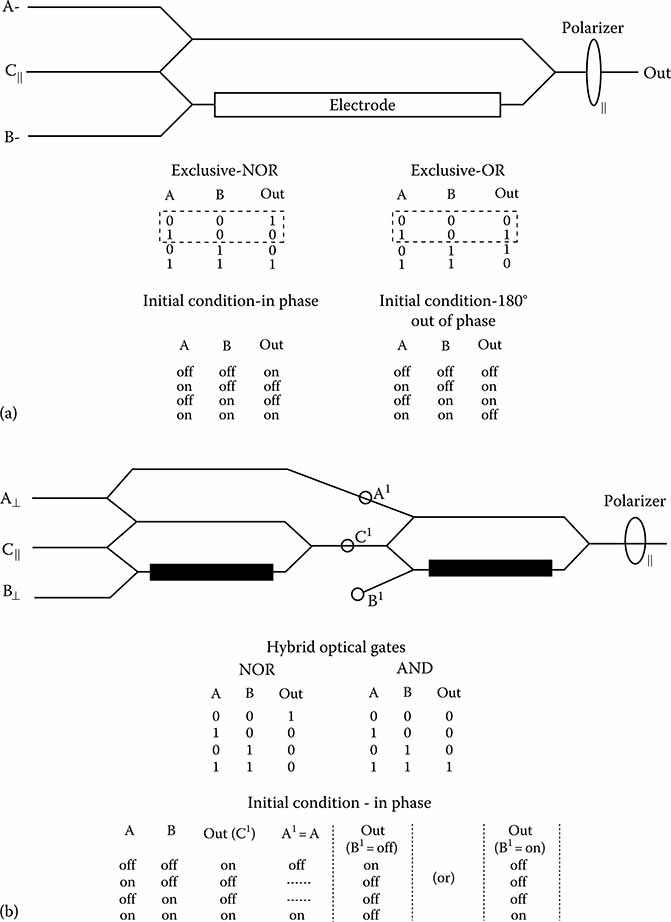
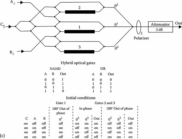
FIGURE 3.16
(a) “Double-Y” Mach–Zehnder interferometer logic gate. (b) Cascade MZI gate. (c) Hybrid MZI gate.
Several combinations of cascaded Double-Y type gates can be considered in order to implement all basic logic functions. Review of Figure 3.16a shows that three logic functions are accounted for by the basic Double-Y gate. Two of these are the ¯XOR
Figure 3.16b shows a cascaded gate that produces either the NOR or AND function, depending on the setting of the B⊥ input. A few of the possible problems that could be encountered in the operation of this gate are the splitting of the A input power and the length of the A⊥ guide. Both of these factors can make the proper phase changes and synchronization difficult to obtain. These problems can be overcome with proper design control. Another problem is the extended length of the device; however, this would be reduced in accordance with reductions in the length of the single Double-Y gate.
Figure 3.16c shows the implementation of the OR and NAND functions. Although structurally more complex than the previous gates, it is a very symmetric design; and therefore, synchronization should be easier to obtain. On the other hand, the effects of the various splitters, combiners, and crossovers will need to be optimized.
A major problem with cascading the Double-Y logic gate is that an “on” output from a following gate cannot be generated by inversion of an “off” output from a previous gate. This is because the individual gates inherently use “on” control pulses. As these are progressively canceled, subsequent gates have fewer operations that can be performed. This is markedly different from electrical logic gates where a source to invert an “off” value is always available.
The MQW Oscillator of interest for optical computing is a hybrid device, which relies on an electrical signal to change the absorptive properties of the material. This change in absorption, caused by the QCSE [42] is a very important effect in MQW structures. These structures are crystals grown by alternating very thin layers of two materials which have similar lattice constants but different band gap energies. A schematic diagram of the material structure and the band diagram of a typical MQW structure is shown in Figure 3.17. The interesting quantum effect arises from the confinement of excitons in the narrow QWs of the material. Confining these excitons, which normally have a radius of about 300 Å, produces two effects. The first is that the exciton absorption line, which normally broadens into the band gap absorption with increasing temperature, remains resolvable even at room temperature. This effect is illustrated in Figure 3.18. The second effect is an induced anisotropy in the effect of an applied electrical field. The exciton absorption line is shifted by an electric field applied perpendicular to the structure layers. This is due to the QW’s enhancement of the exciton binding and consequent avoidance of the exciton dissociation until the higher than normal field strengths. These effects are illustrated in the Figure 3.19.
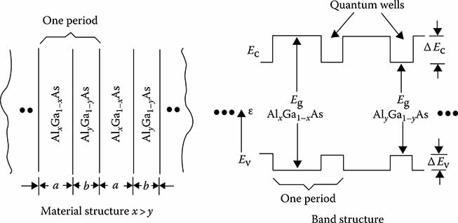
FIGURE 3.17
Multiple quantum well structure.
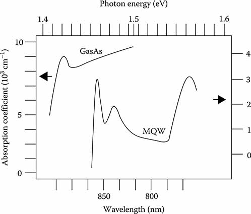
FIGURE 3.18
Linear absorption spectra of room-temperature GaAs and MQW samples. (After Miller, D.A.B. et al., Appl. Phys. Lett., 41(8), 679, 1982.)
3.11 Quantum Well Oscillators
Considerable potential exists for applications of the exciton resonance in MQWS. MQWS are constructed from alternating layers of GaAs and AlxGa1− xAs. When an optical wave is sent through an MQWS, an optical absorption peak which initially creates excitons can be observed near the optical band edge. Excitons are particles described by wave packets made up of electron conduction band states and hole valence band states.
There are two different types of excitons that exist in MQWS. One is an electron-light hole exciton and the other is an electron-heavy hole exciton. Whenever we refer to a “hole” it can be either a heavy hole or a light hole. The excitons that are trapped in the QWs have discrete energy levels that can be described quantum mechanically as the energy levels of a “particle in a box.”
An induced electric field perpendicular to the MQWS layers tends to reduce these energy levels, shifting the absorption peaks to lower frequencies. This shifting effect is nonlinear and smaller for smaller fields. This behavior is known as the QCSC and is analogous to the Franz–Keldysh effect or band-edge shift observed in bulk semiconductors. The shift in exciton energy levels is described as a function of perpendicular electric field intensity. The method used to describe the energy level of excitons in MQWS is to calculate the energy of one exciton in a single QW [41].
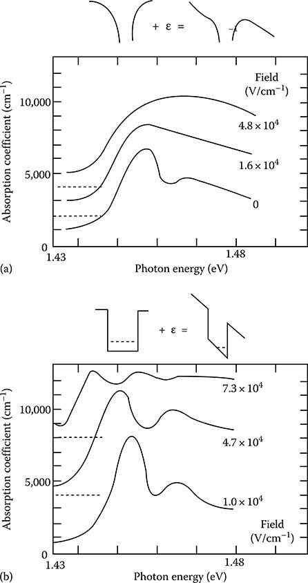
FIGURE 3.19
Absorption spectra at various electric fields for applied (a) parallel, (b) perpendicular, to the QW layer. The distortion is shown schematically. The zeros, indicated by dashed lines, are displaced for clarity. (After Chemla, D.S. et al., J. Opt. Soc. Am., 2(7), 1162, 1985.)
3.11.1 Description of the Quantum Well
The QW is formed by the discontinuities in the energy gap between the GaAs and the AlxGa1−xAs layers. The energy gap difference is described by
ΔEg(eV)=1.425x-0.9x2+1.1x3
where x is the mole fraction of aluminum. This energy gap difference is divided between the hole QWs and the electron QWs. Two theories exist regarding the magnitude of this QW split. The first is an 85:15 split, which means that 85% of the energy gap difference is at the conduction band discontinuity and 15% is at the valence band discontinuity. Another theory suggests a 57:43 split. It is interesting to note that the use of either one of these theories results in little or no difference in the magnitude of the energy shift. Figure 3.17 shows a schematic diagram of a QW structure indicating the band discontinuities.
To describe the exciton’s energy levels in a QW, we must first know the Hamiltonian. The Hamiltonian for this problem can be written as the sum of terms due to the contribution from the individual electron and hole, and the interaction between the two particles.
H=He+Hh+Hex(3.15)
where
He=HKEze+Ve(ze)-eF⊥zeHh=HKEzh+Vh(zh)-eF⊥zhHex=HKEreh+Ve-h(r,ze/zh)
The z direction is defined perpendicular to the MQWS layers and ze and zh are the positions of the electron and hole, while r is the relative position of the electron and hole. The kinetic energy operators in the z direction are defined by
HKEze=-ℏ22m4e⊥xd2dz2eHKEzh=-ℏ22mkh⊥zd2dz2h(3.16)
where
mke⊥x
Ve(ze) and Vh(zh) are the depths of the electron and hole QW potentials
F⊥ is the electric field perpendicular to the MQWS layers
The effective masses for both of the discontinuity split ratios can be calculated as shown in Figure 3.20.
The kinetic energy operator for the interacting particles or exciton and their reduced effective mass are
HKEreh=-ℏ22μd2dr2μ=m*e‖m*h‖m*e‖+m*h‖(3.17)
with m*e||
Ve-h(r,ze/zh)=-e2ε(|ze-zh|2+r2)1/2(3.18)
3.11.2 Solution of the Exciton Energy
The next step to finding the energy levels is to compute the expectation value of H. This gives us the energy of the exciton
Eex=〈Ψ|H|Ψ〉(3.19)
or
Eex=Ee+Eh+Eb
FIGURE 3.20
Effective mass calculation table.
where
Ee=〈Ψ|He|Ψ〉Eh=〈Ψ|Hh|Ψ〉EE=〈Ψ|Hex|Ψ〉
Ee and Eh are the energies of the electron and hole respectively, which can be found using Equation 3.15. EB is the exciton-binding energy which is found using Equation 3.15.
The wave function Ψ is written in a separable form as
Ψ=ψe(ze)ψh(zh)∅e-h(r)(3.20)
where
∅e-h(r)=(2π)1/21λe[-r/λ]
The parameter λ is used as a variational parameter describing the amplitude radius of the exciton.
3.11.3 Determination of Ee and Eh
The problem of determining the energies of the electron and the hole in the QW is subject to a great deal of simplification. Initially it may be noted that, due to the separable nature of the wave function Ψ, Equations 3.19 reduce to the following:
Ee=〈ψe|He|ψe〉Eh=〈ψh|Hh|ψh〉(3.21)
The next simplification is that a wave function describing an electron and hole in an infinite QW can be substituted for the wave function ψe or ψh if an effective well width Lx is used in place of the actual QW width. The longer well width effectively accounts for the fact that there is significant penetration of the wave function into the QW barriers.
The Schrödinger equation for the infinite well barrier in a uniform perpendicular electric field is
-ℏ22m*⊥d2dz2ζ(z)-(W+eF1z)ζ(z)=0(3.22)
where ς(z) is either the electron or hole wave function. Note that the parameters m*⊥
By making the substitution
Z=[2m*⊥(eℏF⊥)2]1/3(W+eF1z)(3.23)
we can transform Equation 3.22 into an Airy differential equation:
ddZ2ζ(z)-zζ(z)=0(3.24)
The solutions have the form
ζ(z)=bAi(Z)+cBi(Z)(3.25)
where b and c are constants and Ai(Z) and Bi(Z) are Airy functions defined by
Ai(Z)=c1f(Z)-c2g(Z)Bi(Z)=√3[c1f(Z)-c2g(Z)]
Further definitions are
f(Z)=1+∞∑n=1Z3n(3n)(3n-1)(3n-3)(3n-4)...3⋅2g(Z)=Z+∞∑n=1Z3n+1(3n+1)(3n)(3n-2)(3n-3)...4⋅3
while c1 = 0.35503 and c2 = 0.25882.
It is convenient to work with dimensionless parameters for the energy and the field. These are defined as
w=WW1;f=FF1
The energy W1 is taken to be the lowest energy level of the particle with zero field. This is simply
W1=ℏ22m*⊥[πLX]2(3.26)
The value W1 is also used to define the unit for the electric field
F1=W2eLX
The values of Z at the QW walls are
Z±=Z(±12LX)
and therefore, using Equations 3.23 and 3.26 Z± becomes
z±=[-πf]1/3(W+12f)(3.27)
If we use the boundary conditions that ς(Z)± = 0 at the QW walls we find from Equation 3.25 a resulting equation which completely determines the eigen energy:
0=Ai(Z+)Bi(Z-)-Ai(Z-)Bi(Z+)
This equation is completely independent of well width and effective mass.
3.11.4 Determination of EB
The exciton-binding energy EB can be rewritten in the following form
EB=EKEr+EpEr(3.28)
EKEr is the kinetic energy of the relative electron–hole motion in the layer plane. It is described by the following equation:
EKEr=〈∅e-h(r)|HKEreh|∅e-h(r)〉=ℏ22μλ2(3.29)
EpEr is the Coulomb potential energy of the electron–hole relative motion.
EpEr=〈Ψ|Ve-h|Ψ〉
In this case, we must use variational wave functions for ψe and ψh in Equation 3.20 [43]. These are written as
ψe,h=N(β)cos[πzLX]exp[-β[ZLX+12]](3.30)
Note that β (βe or βh), Lx (Le or Lh) and z (ze or zh) all depend on whether we are using ψe or ψh. N(β) is a normalization function and is defined such that
N2(β)=4ββ2+n2Lx[1−exp(−2β)]β2
β is a variational parameter and is calculated by minimizing the function E(β) with respect to β2
E(β)=E(0)1[1+β24π2+χ[1β+2β4π2+β2-12coth(β2)]](3.31)
where the ground state energy at zero field is
E(0)1=ℏ2π22m*⊥L2X
and the dimensionless electro-static energy is
χ=|e|F⊥LXE(0)1
This is calculated separately for both the electron and hole.
Using Equations 3.18, 3.20, and 3.30 Equation 3.20 becomes
EpEr=-2e2πελ2N2(βe)N2(βh)2π∫θ=0∞∫r=0Le/2∫ze=−Le/2+Lh/2∫2h=−Lh/2cos2πzeLeexp[-2βe[ZeLe+12]]
cos2πzhLhexp[-2βh[ZhLh+12]]Xrexp(-2r/λ)[(ze-zh)2+r2]1/2dθdrdzedzh(3.32)
The integral over θ is trivial and the integrals over ze and zh must be done using numerical methods. We can calculate the integral over r using the following equation:
G(t)=2λ∞∫r=0rexp(2rλ)dr√t2+r2=2|t|λ[π2[H1(2|t|λ)-N1(2|t|λ)-1]](3.33)
where
H1(u) is the first-order Struve function
N1(s) is the first-order Neumann function or Bessel function of the second kind
The Struve function is defined by [44]
H1(u)=2π[u212⋅3-u412⋅32⋅5+u612⋅32⋅52⋅7-...]
while the Neumann function is defined by [45]
N1(s)=π2πY1(s)+(ln2-ϕ)J1(s)
where φ = Euler’s constant,
Y1(s)=-2sπ+2πln(s2)J1(s)-s2π[∞∑k=0{ξ(k+1)+ξ(k+2)}(-s2/4)kk!(1+k)](3.34)
J1(s)=(s/2)∞∑k=0(-s2/4)kk!(1+k)ξ(1)=-ϕξ(n)=-ϕ+n-1∑k=1k-1n≥2
In summary, to calculate Eb for a particular filed we must first deduce βe and βh for the field, using a variational calculation, and then calculate EKEr and EPEr, adjusting λ variationally to minimize EB.
3.11.5 Effective Well Width Calculations and Computer Simulation
In order to perform all the previous calculations, we must substitute an effective QW width for the actual well width. Note that for an infinite well the wave function has a value of zero outside the well walls. Because the wells in the MQWS are finite, the effective well widths for the infinite well model must be greater than the actual well widths to account for the significant penetration of the wave function into the finite QW barriers. There are two basic ways to find the effective well widths. One way is to try to match the wave functions of the finite well as closely as possible with the infinite well. Another way is to equate the energy of the first energy level in the finite well with the infinite well.
3.11.5.1 Matching of Wave Functions
In order to understand how we match the wave functions, Figure 3.21 shows a finite well wave function where
Ψfinite=ΨI+Ψ11+ΨIIIΨI=2Bcos(κa)ek(z+α)ΨII=2Bcos(κz)ΨIII=2Bcos(κa)ek(z-a)κa tan (κa)=ka(3.35)
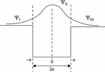
FIGURE 3.21
Finite well wave function.
κa2+(ka)2=2m*⊥a2|VZ|*ℏ2(3.35a)
B is a normalization constant and a is the well half width. Note that the values of mh⊥
Figure 3.22 shows the infinite well wave function where
Ψinfinite=(2LX)1/2cos(πzLX)
Lx is the effective well width and depends on the particle type used in equation.
Figure 3.23 shows both wave functions superimposed. In this figure, the shaded region is the difference in area between the finite and infinite wave functions. The area difference is expressed by the integral
Area difference=∞∫-∞(Ψfinite-Ψinfinite)2dx=∞∫-∞(Ψ2finite-2ΨfiniteΨfinite+Ψ2infinite)dx=2-2+Lz/2∫-Lz/2ΨfiniteΨinfinitedx(3.36)

FIGURE 3.22
Infinite well wave function.
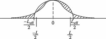
FIGURE 3.23
Infinite and finite well wave functions.
To match these functions as closely as possible, the area between the functions must be minimized.
3.11.5.2 Equating Energy
An alternative method of calculating Lx is to equate the energies of the first energy levels and solve for the length of the infinite QW. The following simple formula is the result:
LX=πκ
where κ is determined from the finite wave function by Equation 3.35.
3.11.5.3 Computer Calculations
In order to complete the calculations described above, computer calculations were used. The first step in calculating the effective width is to find the effective masses using the equations in Figure 3.20. Additionally, the height of the potential well barrier must be calculated using the energy gap difference. The split ratio must be taken into account when finding these two values. By using equations and, the value of κ and k can be found. From these two values, B can be calculated using the fact that
∞∫-∞|Ψfinite|2dx=1
At this point we can calculate the effective width using the equivalent energy method (Section 3.11.5.2) because we know the value of κ. Assuming we have completed the integration in Equation 3.36, we have sufficient information to find the effective width that minimizes the area difference between the two wave functions. The computer can find this effective width iteratively, using Equation 3.36 with different effective well widths until the minimum is found. The values we obtained for several well widths and aluminum concentrations are listed in Figure 3.24.
3.11.6 Summary of Calculation Procedure
With the full theory developed in the previous sections, a brief summary is helpful to explain the steps needed to obtain the exciton energy. Equation 3.19 shows that the exciton energy is broken down into three energy values. The quantum well is fully specified by what may be considered as three “fundamental” values. The aluminum concentrations of the barrier and the well material determine the band gap difference. The other parameter is the actual width of the well.
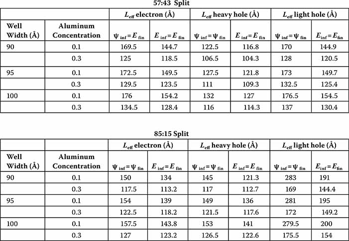
FIGURE 3.24
Effective widths table.
Step A—The effective masses of the particles, the conduction–valence band split, and the effective well widths are found as follows:
A1: The energy gap difference is used to determine the depths of the conduction and the valence band wells. There are the values Ve and Vh. A relatively arbitrary choice is made concerning the ratio of the conductance-valence band split.
A2: Figure 3.20 is used to determine the effective masses of the electrons, and light and heavy holes.
A3: Using the values determined in steps A1 and A2, along with the actual width of the wells, the effective well widths are determined by the methods previously described.
Step B—Values of Ee and Eh are found using the following steps.
B1: A “universal” curve is calculated using Equation 3.27. It is convenient to keep these values as a look-up table since the solution requires an iterative technique. This curve expresses the normalized energy w as a function of the normalized filed f through Equation 3.27.
B2: With a knowledge of w( f ) the actual energy of the particle W (which is actually Ee or Eh) is found by use of the Equation 3.26 to produce W1, F1, f, w, and W.
Step C—Finally, the binding energy EB is determined. For each value of electric field F⊥:
C1: Determine βe and βh for Equation 3.30. This is done by minimizing Equation 3.31 with respect to β.
C2: Using a value of λ and the above values of N2(β) calculate the value of EPEr by performing the double integration over ze and zh in Equation 3.32.
C3: Calculate EEEr using Equation 3.29.
C4: Repeat steps C2 and C3, adjusting λ to minimize EB.
C5: Start at step C1 for the next field value.
Again, it is useful to use look-up tables for parts of Step C—in particular for the values of Equation 3.33.
3.11.7 Example: Fabrication of MQW Oscillator
An MQW could be fabricated from GaAs/AlGaAs heterostructure such as that shown in Figure 3.25. This structure would require about five mask and fabrication steps. The thin optical window, with no field applied perpendicular to the QW junction layers, will be transparent to a wavelength—denoted λlow—of slightly lower energy than the absorption peak. Application of a filed will shift the absorption peak to lower energies and the window will become opaque to the incident wavelength λlow. This operation, depicted in Figure 3.26 [41] shows the transmission of the device as a function of the applied bias. The proposed vertical material structure is shown in Figure 3.27 [46]. Figure 3.28 shows a photoluminescence scan of the material taken at room temperature (~300 K). Various important features and their wavelengths and corresponding photon energies are indicated in the figure. Most notable are the obviously well-defined exciton emissions, which would not be observable at room temperature without the QW structures. Peak 1 indicates the exciton from the equal width QW structure, denoted period B in figure. Peak 2 shows the emission from the unequal, period A wells. Peak 3 indicates emission from the wide band gap AlGaAs p-type cap layer (layer 8 in Figure 3.27). The energy of emission corresponds to an aluminum concentration of approximately 32%. Figure 3.29 shows another photoluminescence scan performed on the sample at a temperature of 12 K. Two effects are noted. First is the shift of the peaks. The second is the sharpening of the peaks due to the decrease of the phonon energy broadening.

FIGURE 3.25
Optical QW oscillator modulator.
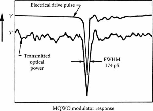
FIGURE 3.26
MQWO modulator response.
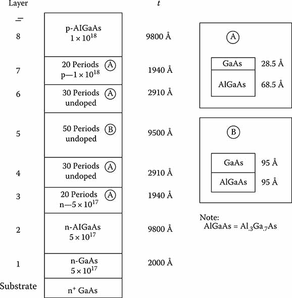
FIGURE 3.27
MQWO device structure.
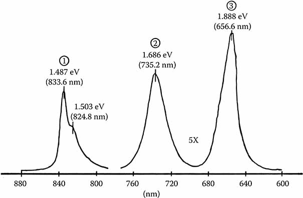
FIGURE 3.28
Photoluminescence scan of MQWO device at room temperature.
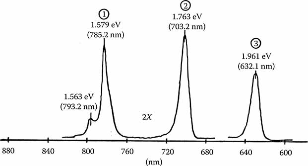
FIGURE 3.29
Photoluminescence scan of MQWO device at 12 K.
3.12 Design Example: Optically Addressed High-Speed, Nonvolatile, Radiation-Hardened Digital Magnetic Memory
Military and space applications require a number of unique memory characteristics. These include [47] nonvolatility, maintainability, security, low power and weight, small physical size, radiation hardness, and the ability to operate in severe environments (temperature, humidity, shock and vibration, and electromagnetic fields). The need for radiation hardness is of special interest where the use of various directed energy weapons (DEW) against satellite assets is anticipated. The goal of DEW is to destroy at least part of the threat nuclear warheads in the exoatmosphere. This scenario will expose the on-board electronics and associated computer memory to many types of high-level radiations.
Considering these requirements, along with the goals of further improved life cycle cost, programmability, speed, volume, and power consumption of present devices—the crosstie memory system discussed herein represents an excellent choice for nonvolatile memory in a radiation environment. The design discussion increases the read speed of this memory by more than an order of magnitude, providing the possibility for multiple applications.
3.12.1 History of the Magnetic Crosstie Memory
The crosstie magnetic effect in thin film magnetic material was discovered in 1958 by E.E. Huber. The magnetic thin film exists in two possible magnetic states: the Neel wall state which represents the fundamental magnetic domain wall; and the crosstie/Bloch line pair on the Neel wall, which represents the second magnetic domain state. The crosstie wall constitutes a transition form between Bloch walls of very thick films and the Neel walls of very thin films. As the film thickness is decreased, the Neel wall forms segments of opposite polarity, which reduces the magnetostatic energy in the wall. These segments are separated by perpendicular magnetization circles called Bloch lines, which minimize energy by forming spiked walls or crossties on alternate Bloch line locations. The crosstie Bloch line pairs represent digital information stored in the computer memory.
Work began in the early 1970s to develop a computer memory utilizing serrated strips of thin film 80–20 Ni–Fe permalloy data tracks that stored information in a series of crosstie Bloch line patterns on a Neel wall. The concept was similar to the serial propagation of bubbles in a magnetic bubble memory, but promised faster performance. The serial crosstie memory presented numerous development problems, however, illustrating the need for an alternative approach [48]. The random access approach was successfully demonstrated in early 1982 by Mentzer, Schwee et al. [49]. Its unique characteristics as a faster, nonvolatile, radiation- and temperature-insensitive, random access device make the crosstie memory a viable alternative for many applications. More recently [50], this technology is being developed for alternative flash memory, fast-start computer systems, biomedical storage devices, and dynamic RAM replacement. Significant efforts are underway as of this writing at IBM, Infineon, Naval Research Laboratory, and elsewhere.
3.12.2 Fabrication and Operation of the Crosstie Memory
Thin film permalloy (81–19 Ni–Fe) patterns on a silicon substrate support stable magnetization domain states which can be switched rapidly and detected nondestructively. The geometry of the basic memory cell is shown in Figure 3.30 [51]. The contours represent the direction of magnetization in the memory cell. The cell on the left represents a digital zero (Neel wall); and the cell on the right represents a digital one state (crosstie Bloch pair on Neel wall). The crosstie wall constitutes a transition state between Bloch walls of thick films and Neel walls of very thin films. The fundamental cell geometry supports two states—the Neel wall and the Bloch line-crosstie pair on the Neel wall.
Vacuum deposition of the permalloy alloy is performed in a magnetic field resulting in approximately 400 Å isotropic films with Hk < 10 Oe. Silicon substrate temperature and alloy stoichiometry are such that the material displays zero magnetostriction and maximum magnetoresistance ΔR/R > 2%. This ratio indicates the differential resistance between fields applied parallel and perpendicular to permalloy current flow, divided by the permalloy resistance. The current method of detecting the memory state utilizes this effect.
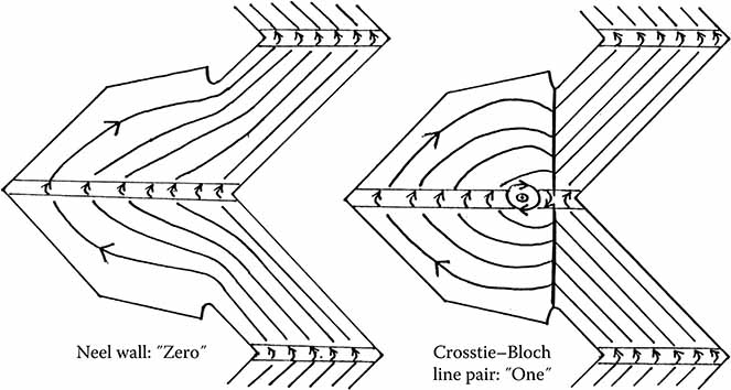
FIGURE 3.30
Magnetic domain pattern in CRAM storage element.
Switching between digital information states is accomplished through application of coincident in-plane fields (~10 Oe) produced by 5–7 mA currents flowing through overlying row and column conductors. The magnetic film changes states when a sufficient current is placed in the local area. Therefore, the column conductors zig-zag or meander in order to align the local electromagnetic fields of the column conductor with the row conductor in the local area of the memory cell. The test chip described by Mentzer et al. [52] (Figure 3.31) consisted of four 64-bit columns, a fifth reference column, column meander columns, column meander conductors, and four row conductors, providing access to 16 test bits. Five vacuum depositions and five photolithographic steps are required to fabricate the device. The permalloy memory cells are followed by a sputtered silicon nitride dielectric layer with vias for contacts to the permalloy, metallization for row conductors and contacts to the permalloy, another dielectric layer, and metallization for column conductors.
The electronic method for nondestructive read-out (NDRO) is performed by applying a positive field less than the annihilation level using the appropriate row conductor. The permalloy thin film has current applied. Therefore, when the current in the row conductor passes through a memory cell location in a crosstie state, a differential voltage is created. The differential detection voltage for a single bit obtained when a field is applied in the annihilation direction but less than the annihilation threshold is less than 300 μv. This low-detection signal level represents a significant challenge to the widespread implementation of the crosstie memory. As a result, Mentzer et al. [53] devised a signal extraction and processing architecture (Figure 3.32), which improved the signal level but increased the complexity of the device significantly.
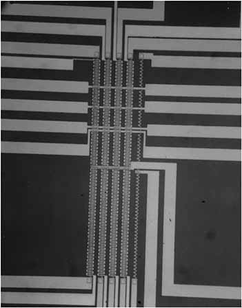
FIGURE 3.31
Photomicrograph of 4 × 64 crosstie memory array.
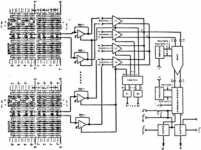
FIGURE 3.32
Signal extraction and processing architecture for CRAM.
The Mentzer/Lampe technique utilizes double-correlated sampling to remove offset nonuniformity fixed patterns by means of serial subtraction. Postdetection integration is implemented where signals accumulate constructively and directly while temporal noise is uncorrelated and adds only in terms of power. Integration of four such samples effectively doubles the signal to noise ratio. This approach also severely reduces the achievable memory density and increases power consumption, since the dominant factor dictating both density and power consumption is the size of the current drivers required to supply current through the permalloy columns. Clearly a technique is needed whereby the detection scheme is improved, in favor of a more direct readout—but still utilizing all of the useful features of the memory device (electronic write, radiation hardness, etc.).
3.12.3 Potential Optical Detection Scheme
Optical detection could supplant the magnetoresistance detection approach, which limits access times to approximately 500 ns. This is too slow for many primary memory applications. The optical technique will afford read-write cycle times that are competitive with the fastest available technologies on the market. In fact, the crosstie memory access times may prove to be the fastest achievable, with the optical addressing scheme described herein.
The detection circuit for the optical detection (read) scheme requires simpler circuitry; so there will be not only performance gain but also significant improvement in cost and producibility. Additional limitations of the magnetoresistance effect include the requirement to heat the substrate to increase crystallite size and to provide the necessary magnetoresistance ratios, along with temperature limitations. These limitations are eliminated with optical access and detection using the Faraday magneto-optic effect.
Magneto-optic Faraday rotation occurs when linearly polarized light is transmitted through a material parallel to the direction of a magnetic field in the material. The amount of rotation φ is proportional to the magnetic field M and the path length t, such that φ = VHt cos θ, where V is the Verdet constant (rotation per unit length per unit magnetic field), and θ is the angle between the magnetic field and direction of light propagation. In the proposed crosstie memory detection configuration, the presence or absence of a crosstie wall is used to produce a change in the transmitted optical power density through crossed polarizers that are rotated from extinction by an angle equal to the amount of Faraday rotation produced. Differences in transmitted light intensity through different memory locations thus provide detection of stored information. The Neel wall state does not have a magnetic field perpendicular to the permalloy surface while the crosstie state does.
Figure 3.33 shows the permalloy pattern to be used to write information on the memory device. Creation of crossties is performed by the application of coincident currents flowing through conductor strips insulated by nitride layers. Windows should be added to the nitride and conductor layers to define the spot size of the transmitted light for optical detection of the crossties. Polarizers can be either grown or bonded to the device as wafer processing permits. Laser radiation will be applied through a particular memory block or array accessed via electro-optic switching.
Detection of transmitted light intensity is accomplished with a silicon PD array. Random access or parallel addressed read may also be accomplished through the detector array, rather than electro-optic switching. Current levels produced by changing light intensities resulting from partial extinction of Faraday rotated light are amplified and coupled to a comparator with sensitivity controls allowing identification of logic levels. The device configuration is illustrated at Figure 3.34.
Assuming a crosstie magnetic field equal to the saturation magnetization, we have a specific Faraday rotation in permalloy equal to 1–2 × 10⁵ deg cm−1. This provides a rotation of approximately 2° with a permalloy thickness of 600 Å, at λ0 = 830 nm. Thin film and multilayer dielectric polarizers supply a 3.5% change in transmitted intensity per degree of analyzer rotation with the polarizer at 45° from extinction with respect to the input polarization. A fixed insertion loss of 15% for the polarizers, and a loss due to absorption in the permalloy of 2.7% for 600 Å thickness (α = 6 × 105 cm−1) along with a 50% loss due to initial polarizer rotation, provide a decrease in optical power density form polarizer to detector of 65%. This level is decreased by 3.5% polarizer transmittance per degree of rotation X2 = 7% due to the presence of a crosstie. If we couple 3 mW of power into the system, the PDs will see changes of 74 μW on a background of 1050 μW.
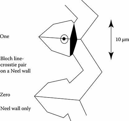
FIGURE 3.33
Permalloy array pattern.
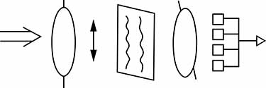
FIGURE 3.34
Optical detection format.
PDs can produce 25 mV μW−1 μs−1 integration time at 12 μm center-to-center spacings. A power level of 1050 μW then provides a 650 mV signal using 25 ns integration time, with a 46 mV change in voltage for crosstie detection. Excellent signal to noise ratios are thus possible for low false alarm probabilities. The signal may be compared to a reference zero location electro-optically switched simultaneously, and differentially amplified for further signal processing. Such a system provides excellent high-speed detection for the crosstie memory, and eliminates the problems associated with electrically addressed readout.
3.12.4 Radiation Hardening Considerations
Radiation environments in which such a memory may be required to survive are a strong function of the particular system deployment. Tactical man-operated systems are required to survive only modest ionizing dose rates, low accumulated doses and low neutron levels, with man being the limiting factor. Strategic ground-based systems are required to withstand sharply higher levels. Space-based systems with no nuclear weapon environment must survive only the natural Van Allen belt energetic electron and proton environments, which may range up to several tens of kilorads (Si0) depending on the orbit and the duration of the mission. Military systems in space must survive the nuclear weapon environments of high ionizing dose rates, high accumulated doses and neutron fluences. The system memory requirements in terms of organization, power, speed, etc., will all be different in each of these applications; but in general will tend toward higher speed, low power, high density, nonvolatility, and low soft error rates.
The optical read crosstie memory discussed affords all these features in addition to nuclear hardness. Since the optically read memory is inherently free from soft errors, there will be no need to increase the word length to allow for error detection and correction. Normally, 5 bits of a 16 bit word are utilized for double error, single error correction; so an immediate savings of 30% of the memory size and power supply requirement is realized. The radiation environments in which memories may be required to survive vary with application, but may include ionizing dose rates in excess of 1012 rad (Si)/s, total accumulated doses of up to 107 rad (Si), and neutron fluences of up to 1014 n cm−2.
References
1. Oakley, W. S. October 1979. Acousto-optic processing opens new vistas in surveillance warning receivers. Defense Electron. 11:91–101.
2. For the relations between index change and acoustic power, see: Pinnow, D. 1970. Guidelines for the selection of acoustooptic materials. IEEE J. Quant. Electron. 6:223–238.
3. Korpel, A. January 1981. Acousto-optics—A review of fundamentals. IEEE Proc., Vol. 69(1):48–53.
4. Chang, I. C. March 1986. Acousto-optic channelized receiver. Microwave J. 29:142, 142–144.
5. Oakley, W. S. Acousto-optic processing opens new vistas. Defense Electron.
6. Chang, I. C. 1986. Acousto-optic channelized receiver. Microwave J. 29:141–144.
7. Tsui, J. B. 1983. Microwave Receivers and Related Components, Chap. 7, Avionics Laboratory, Air Force Wright Aeronautical Laboratories. NTIS.
8. Main, R. P. Fundamentals of acousto-optics. Laser Appl. June 1984:111.
9. Lawrence, M. November 1984. Acousto-optics may replace electronic processing. Microwaves RF.
10. Oakley, W. S. Acoustooptic processing opens new vistas. Defense Electron.
11. Mellis, J., G. R. Adams, and K. D. Ward. February 1986. High dynamic range interferometric Bragg cell spectrum analyser. IEEE Proc. J. 133(1):26–30.
12. Hamilton, M. C. January–February 1981. Wideband acousto-optic receiver techniques. J. Electron. Defense.
13. Kalman, R. and I. C. Chang. 1986. Acousto-optic Bragg cells at microwave frequencies. Proceedings of SPIE 639.
14. Ibid.
15. Ibid.
16. Lawrence, M.J., B. Willke, M.E. Husman, E.K. Gustafson, and R.C. Byer. 1999. Dynamic response of a Fabry-Perot interferometer. J. Opt. Soc. Am. B. 16(4):523–532.
17. Tsui, J. B. 1983. Microwave Receivers and Related Components. Chapter 1. Avionics Laboratory Air Force Wright Aeronautical Laboratories. NTIS.
18. Ibid.
19. Oakley, W. S. Acousto-optic processing opens new vistas. Defense Electron.
20. Borsuk, G. M. January 1981. Photodetectors for acousto-optic signal processors. IEEE Proc. 69(1):100–118.
21. Ibid.
22. Ibid.
23. Tsui, J. B. Microwave Receivers and Related Components. Avionics Laboratory.
24. Borsuk, G. M. 1981. Photodetectors for acousto-optic signal processors. IEEE. 69(100):100–118.
25. Mellis, J., G. R. Adams, and K. D. Ward. 1986. High dynamic range interferometric Bragg cell. IEEE Proc. J. (1):26–30.
26. Borsuk, G. M. Photodetectors for acousto-optic signal processors. IEEE.
27. Hamilton, M. C., D. A. Wille, and W. J. Miceli. 1977. Opt. Eng. 16:467.
28. Barnoski, M. K., B. Chen, H. M. Gerard, E. Marom, O.G. Ramer, W.R. Smith Jr., G.L. Tangonan, R.D. Weiglein. 1978. Design, fabrication and integration of components for an integrated optic spectrum analyzer. Paper Presented at the IEEE Ultrasonics Symposium. IEEE Trans. on Sonics and Ultrasonics. 26(2):146.
29. Mergerian, D., E. C. Malarkey, R. P. Patienus et al. September 1980. Operational integrated optical RF spectrum analyzer. Appl. Optics 19(18):15.
Mergerian, D., E. C. Malarkey, M. A. Mentzer. 1982. Advanced integrated optic RF spectrum analyzer. Proceedings of SPIE. Conference on Integrated Optics II, January 28–29, Los Angeles, CA. 321:149.
30. Casasent, D. June Short course at Carnegie Mellon, 1981. Optical signal processing. Electro Optical Systems Design.
31. Ibid.
32. Ibid.
33. Mentzer, M. A., S. T. Peng, and D. H. Naghski. 1987. Optical logic gate design considerations. Proceedings of SPIE 835 Integrated Optical Circuit Engineering V., Mark A. Mentzer, ed., August 17–20, pp. 362–377, San Diego, CA.
34. Gibbs, H. M., S. L. McCall, and T. N. C. Venkatesan. 1980. Optical bistability. Opt. Eng. 19:463.
35. Gibbs, H. M., S. L. McCall, T. N. C. Venkatesan, A. C. Gossard, A. Passner, and W. Wiegmann. 1979. Nonlinear optical materials. Appl. Phys. Lett. 35:451.
36. Esaki, L. and R. Tsu, 1970. Superlattice and negative differential conductivity in semiconductors. IBM J. Res. Dev. 14:61–65.
37. Gibbs, H. M., S. L. McCall, T. N. C. Venkatesan. 1976. Differential gain and bistability using a sodium-filled Fabry-Perot interferometer. Phys. Rev. Lett. 36:1135.
Smith, P. W., E. H. Turner, and P. J. Maloney. 1978. Electro-optic nonlinear FabryPerot devices. IEEE J. Quant. Electron. QE-14:207.
Jewell, J. L., Y. H. Lee, M. Warren. 1985. GaAs étalon optical logic devices. Appl. Phys. Lett. 46:918.
38. Martin, W. E. 1975. Refractive index profile optimization. Appl. Phys. Lett. 26:562.
Ramaswami, V., M. D. Divino, and R. D. Stanley. 1978. Appl. Phys. Lett. 32:644.
39. Lattes, A., H. A. Haus, F. J. Leonberger, and E. P. Ippen. 1983. An ultrafast all-optical gate. IEEE J. Quant. Electron. QE-19 (11):1718.
Haus, H. A., N. A. Whitaker, Jr., and M. C. Gabriel. 1985. All-optical logic devices using group III–IV semiconductor waveguides. Proceedings of SPIE 578 Integrated Optical Circuit Engineering III, p. 122.
40. Mentzer, M. A., S. T. Peng, and D. H. Naghski. Optical logic gate design considerations. SPIE.
41. Wood, T. H., C. A. Burr, D. A. B. Miller, D. S. Chemla, and T. C. Damen. 1985. IEEE J. Quant. Electron. QE-21 (2):117.
42. Mentzer, M. A., S. T. Peng, and D. H. Naghski. Optical logic gate design considerations. SPIE, pp. 362–377.
43. Bastard, G., E. Mendez, L. H. Chang, and L. Esaki. 1983. Variational calculations on a quantum well in an electric field. Phys. Rev. B 28 (6):3241.
44. Abromowitz, M. and I. Stegan, eds. 1972. Handbook of Mathematical Functions with Formulas and Graphs. New York: John Wiley and Sons p. 496.
45. Ibid., p. 360.
46. Miller, D. A. B., D. S. Chemla, D. J. Eilenberger, D. J. Smith, P. W. Gossard, and W. T. Tsang. 1982. Optical bistability due to increasing absorption. Appl. Phys. Lett. 41(8):679.
47. Lo. D. S. Nov. 1984. Selecting memory devices for military applications. Defense Electron.
48. Schwee, L. J., P. E. Hunter, F. A. Restorff, and M. T. Shepard. 1982. CRAM Concepts and initial studies. J. Appl. Phys. 53(3):2762.
49. Mentzer, M. A., C. W. Baugh, E. A. Hubbard. 1982. Fabrication and characterization of a crosstie random access memory. IEEE Trans. Magnetics, 3IM3 Conference, July, Montreal, Quebec.
50. Slaughter, J. M. August 2009. Materials for magnetoresistive random access memory. Annu. Rev. Mater. Res. 39:277–296.
51. Mentzer, M. A., C. W. Baugh. 1982. Magnetic crosstie random access memory. Best Paper Award. Government Microcircuit Applications Conference, Orlando, FL.
52. Ibid.
53. Mentzer, M. A., D. Lampe. 1984. Signal processing and architecture for the cross-tie random access memory. Presented at Government Microcircuits Applications Conference, Las Vegas, NV.