
2
Electro-Optics
2.1 Introduction
Developing communication, instrumentation, sensors, biomedical, and data processing systems utilize a diversity of optical technology. Integrated optics is expected to complement the well-established technologies of microelectronics, optoelectronics, and fiber optics. The requirements for applying integrated optics technology to telecommunications have been explored extensively and are well documented [1]. Other applications include sensors for measuring rotation, electromagnetic fields, temperature, pressure, and many other phenomena. Areas that have received much recent attention include optical techniques for feeding and controlling GaAs monolithic microwave integrated circuits (MMIC), optical analog and digital computing systems, and optical interconnects for improving integrated system performance [2].
An example of an MMIC application [3] is a fiber-optic distribution network interconnecting monolithically integrated optical components with GaAs MMIC array elements (see Figure 2.1). The particular application described is for phased array antenna elements operating above 20 GHz. Each module requires several RF lines, bias lines, and digital lines to provide a combination of phase and gain control information, presenting an extremely complex signal distribution problem. Optical techniques transmit both analog and digital signals as well as provide small size, light weight, mechanical stability, decreased complexity (with multiplexing), and large bandwidth.
An identical RF transmission signal must be fed to all modules in parallel. The optimized system may include an external laser modulator due to limitations of direct current modulation. Much research is needed to develop the full compatibility of MMIC fabrication processes with optoelectronic components. One such device being developed is an MMIC receiver module with an integrated photodiode [4]. Use of MMIC foundry facilities for fabrication of these optical structures is discussed in Section 5.11.
Another application area that can significantly benefit from monolithic integration is optically interconnecting high-speed integrated chips, boards, and computing systems [5]. There is ongoing demand to increase the throughput of high-speed processors and computers. To meet this demand, denser higher speed integrated circuits and new computing architectures are constantly developed. Electrical interconnects and switching are identified as bottlenecks to the advancement of computer systems. Two trends brought on by the need for faster computing systems have pushed the requirements on various levels of interconnects to the edge of what is possible with conventional electrical interconnects. The first trend is the development of higher speed and denser switching devices in silicon and GaAs. Switching speeds of logic devices are now exceeding 1 Gb/s, and high-density integration has resulted in the need for interconnect technologies to handle hundreds of output pins. The second trend is the development of new architectures for increasing parallelism, and hence throughput, of computing systems.
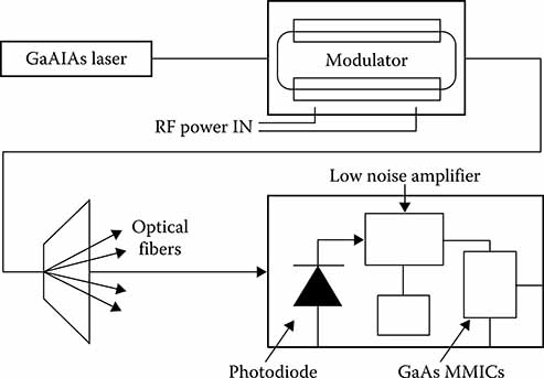
FIGURE 2.1
Optical signal distribution network for MMIC module RF signals.
A representation of processor and interconnect complexity for present and proposed computing architectures [6] is shown in Figure 2.2.
The dimension along the axis is the number of processors required for various architectures. On the left side is the Von Neumann architecture with relatively few but very complex processors. Progressing to the right, the number of processors per system increases, until it reaches a neural network requiring millions of processors, but of much lower complexity than the Von Neumann case. Looking at Figure 2.2, it becomes apparent that as the number of processors increases, the number and complexity of interconnects within the system increases dramatically. In fact, on the far right of the scale, the interconnects become an integral part of the computing architecture, and the boundary between the processors and the interconnects becomes blurred.
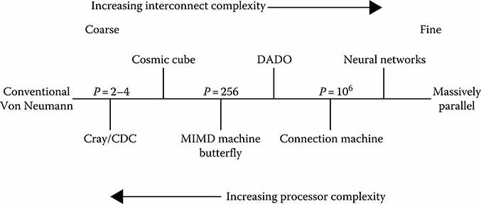
FIGURE 2.2
Processor versus interconnect complexity.
2.2 Optical Device Applications
The purpose of this section is to examine recent advances in GaAs technology with respect to optics applications and fabrication requirements. It will be seen that, by integrating GaAs devices and fabrication techniques into the design and development of optical circuits, many of the problems that could hinder the production of reliable and high-speed optical structures may be overcome.
Initial circuits designed were for the S to X bands, but the range of MMIC applications has now been extended as low as 50 MHz and as high as 100 GHz [7]. Frequency ranges through UHF will most likely make more use of the presently available high-speed integrated circuit silicon-based technologies than the MMIC technology. MMIC will be used in a wide variety of electronic warfare applications, such as decoys and jammers, and in phased array radars. In the commercial markets, there will be uses for MMIC technology in consumer communications’ products and automotive sensors and global positioning systems. Satellite systems will be redesigned using large-scale integration and MMIC techniques to improve reliability and increase functional capacity. One of the applications of optics technology to microwave systems that has received a great deal of attention in the past few years is the use of fiber-optic modules and feed structures to replace the large and unwieldy feed structures of past phased array radar systems. The phased array technology is described in Section 2.2.1.
2.2.1 Phased Array Radar
The key item that distinguishes phased array radar from other radars is the distributed antenna configuration. The existence of an antenna array does not necessarily indicate a phased array. As defined by Liao [8], a phased array is an antenna array whose main beam maximum direction or pattern shape is controlled primarily by the relative phase of the element excitation currents. As an example, consider Figure 2.3 depicting a simple linear array arranged along the z-axis. Following the analysis in Stutzman and Thiele [9], the current in each element is represented as
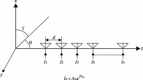
FIGURE 2.3
Excitation current relationship of a linear phased array.
I0=Ane-ian(2.1)
The array is of linear phase if the elements are phased so that
an=-Bzncosθ(2.2)
It follows from Figure 2.3 and Equations 2.1 and 2.2 that if the phase of each element is changed with time, the direction of the main beam θ is scanned. The ability to alter the direction of the main beam electronically provides the radar designer with a myriad of scanning options from which to choose.
A typical phased array radar configuration is shown in Figure 2.4, with a typical conventional radar system block diagram for comparison shown in Figure 2.5. All of the functional areas outlined in Figure 2.5 are maintained by the phased array system, but the distribution of duties has been modified. The T/R modules perform several functions that are taken care of in the beam steering, transmission, and reception functional areas in the generic radar system of Figure 2.5. The array processor performs the functions of the processor in Figure 2.5 as well as handles some of the demodulation and detection functions that were performed by the receiver. The signal generator in Figure 2.4 is accountable for the transmitter duties that are not carried out by the T/R modules. The array controller in the phased array configuration generates the phase shifting and transmits/receives switching information required by the T/R modules, and for controlling the signal generator and array processor. In addition, the array controller converts the data obtained from reflected signals by the array processor into a format for display to the system operator.

FIGURE 2.4
Typical phased array radar configuration.
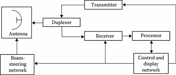
FIGURE 2.5
Block diagram of a typical radar system.
The distributed nature of the radar formation in Figure 2.4 yields several operational advantages over conventional radar systems. For instance, by dividing the power amplification duties over what is typically thousands of T/R modules, solid state amplifiers may be used instead of tube-based amplifiers. This provides a decrease in size and cost per amplifier and an increase in reliability.
Another advantage realized in phased array radar designs is high-speed beam steering and radiation pattern control. Since the beam characteristics are determined by the relative current phases of the radiating elements, the array controller has complete and nearly instantaneous control over the beam direction and pattern. For the same reasons, the phased array system is an ideal candidate for computer control due to the ability to control the array beam characteristics via the phase shifters located in the T/R modules. This ability is enhanced since the phase shifters most commonly chosen for modern T/R modules are digital; therefore, the operator could run any number of phase sequencing algorithms from a computer controller to maneuver the radar beam.
The physical layout of the phased array provides some additional advantages over the nonarray radar. First, since there are typically thousands of radiating elements in a phased array radar, the system may exhibit non-catastrophic degradation. If a small percentage of the radiating elements are nonoperational, the radar will function properly but generally with an increase in peak sidelobe level [10]. Also, since phased arrays are typically built in a planar arrangement, they are more resistant to blasts, making the phased array attractive for use in hostile environments.
One of the major design decisions for a phased array radar is the choice of an array feed formation. Several options are available including the one source, one feed design implied in Figure 2.4. Figure 2.6 depicts a few other alternatives. One common implementation is the multiple-source corporate fee. An example of this is the COBRA DANE system located on Shemya Island, Alaska. This inbound and outbound missile tracking radar uses 96 traveling wave tubes to illuminate its 15,360 active elements [11]. The serpentine feed structure is being incorporated in the S-band AR320 3-D Radar [12].
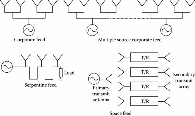
FIGURE 2.6
Array antenna feed configurations.
Another key consideration is that of operating frequency. As the radar operating frequency increases, the size of the antenna decreases, thereby enhancing the mobility of the system; however, since the antenna is smaller, either the size of the T/R module in Figure 2.4 must decrease proportionally or each source must feed a larger number of radiating elements.
The preceding considerations indicate much of the difficulty in phased radar development is mechanical in nature. One additional mechanical consideration leads to perhaps the primary reason for the lack of widespread phased array deployment. Each of the several thousand radiating elements in a phased array must be manufactured to exacting tolerances— each shifted to a high degree of accuracy. The sheer number of specialized elements makes cost the primary design driver. Tang and Brown [13] cite the following factors as the major contributors to the high cost of system development:
A large number of discrete components in conventional array antenna.
Poor production yields of high-power amplifiers.
High labor costs due to tight manufacturing tolerances.
Lack of dedicated production lines due to limited quantities.
The MMIC technology promises to overcome these problems, so that the phased array technology can come to full fruition.
2.2.2 GaAs Field Effect Transistor Technology
The advantages of GaAs are utilized in many recent developments in discrete GaAs field effect transistor (GASFET) technology. Gain and relatively low-noise characteristics were demonstrated by several manufacturers into the millimeter wave region. (In comparison, silicon devices are typically limited to applications below X-band.) In addition to its proven microwave performance, GASFET technology is readily integrated onto a common substrate with optical and optoelectronic components, permitting the development of optical monolithic microwave integrated circuit (OMMIC) systems. Since the GASFET is the basic building block of the MMIC technology, a discussion of FET structures and processes follows.
The FET is a three-terminal unipolar device in which the current through two terminals is controlled by the voltage present at the third. The term “unipolar” indicates that the FET uses only majority carriers to handle the current flow. This characteristic provides the FET with several advantages over bipolar transistors [14]:
It may have high-voltage gain in addition to current gain.
Its efficiency is higher.
Its operating frequency is up to the millimeter region.
Its noise figure is lower.
Its input resistance is very high, up to several megaohms.
Unipolar FETs come in two basic forms: the p-n junction gate and the Schottky barrier gate.
The first FET structure to be discussed is the p-n junction FET, or JFET. The basic physical structure of the JFET is shown in Figure 2.7a [15]. The n-type material sandwiched between two p+-type material layers acts as the channel through which the current passes from the source to the drain of the device. The voltage applied to the gate contacts of the device determines the width of the depletion region and therefore the width of the channel. A reverse bias between the p+-type layers causes the depletion regions to cross over into the n-type channel region. Since the channel region has fixed resistivity due to its doping profile, the resistance of the channel will vary in response to the changes in the effective cross-sectional area. With the n-type channel configuration shown in Figure 2.7a, the electrons flow from the source to the drain. This flow would be from the drain to the source for a p-type channel sandwiched between n+-type gate regions. Figure 2.7b [16] depicts the restriction of the conduction channel by an increase in drain voltage. As VD increases, so does ID, which tends to increase the size of the depletion regions. The reverse bias, being larger toward the drain than toward the source, generates the tilt in the depletion region toward the drain. Since the resistance of the restricted conduction channel increases, the I–V characteristic of the channel diverges from linear. As VD increases more, there is a point at which the value of ID levels off and the channel is completely pinched off by the depletion regions. Once the device is in this saturated operating region, the drain current may be modulated by varying the gate voltage.
The JFET was the first variety of field effect device developed and is still found in many applications. Its structure, however, requires a multiple-diffusion process and so makes it a difficult device to integrate. The device is also limited to frequencies below X-band due to the slow transit times under the diffused gate regions.
The Schottky barrier gate FET is of most interest for the development of OMMICs. Schottky suggested in 1938 that a potential barrier could arise from stable space charges in the semiconductor without the introduction of a chemical layer. This provided the foundation for the development of the metal semiconductor FET (MESFET).
The physical structure of the MESFET is shown in Figure 2.8. This particular GASFET is a low-noise device that has been fabricated using ion implantation techniques. This technique will be compared with others for the mass production of MMIC devices in Sections 5.10 and 5.11. The device fabrication process begins with the implantation of donor ions (in this case, Si+ ions) directly into a semi-insulating GaAs substrate wafer. Next, n+ contact layers are implanted into the source and drain contact regions to help reduce the source resistance. The FET source and drain ohmic contacts are formed next using gold alloys. High temperatures are used to bond the contacts and to ensure smooth edges. The contact photolithography process continues with the formation of the gate metallization. This is the most critical step of the process since the gate metallization is typically 0.5 μm long by 300 μm wide and forms the space charge, or depletion, region. The gate metallization is generally an aluminum alloy.
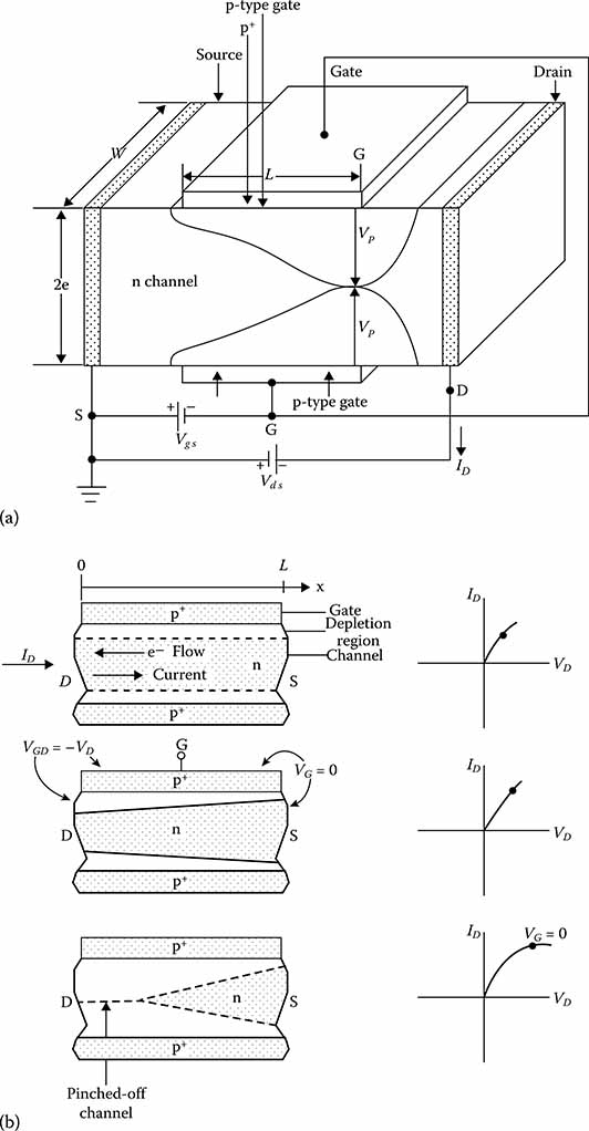
FIGURE 2.7
JFET structure and characteristics (a) p-n junction gate FET (JFET) and (b) JFET channel depletion characteristic.
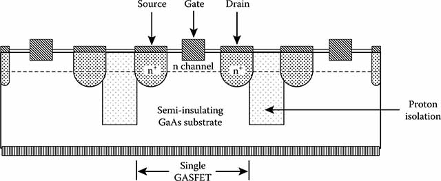
FIGURE 2.8
Integrated GASFET structure cross section. (Adapted from K. Wang and S. Wang, “State-of-the-art ion-implanted low-noise GaAs MESEFETs and high-performance monolithic amplifiers.”)
The MESFET in Figure 2.8 has a gate made of titanium and aluminum and then overlayered with a titanium and gold mixture for a low-resistance bonding. In MMIC fabrication, device isolation is an important factor in reducing RF losses. Good isolation and a reduction in pad capacitance are achieved, as shown in Figure 2.8, by direct proton bombardment [17].
The basic operation of the MESFET has been described by Liao [18]: “A voltage is applied in the direction to reverse bias the n+-n junction between the source and gate, while the source and drain electrodes are forward biased. Under this bias condition the majority carrier electrons flow in the n-type layer from the source electrode, through the channel beneath the gate, to the drain electrode. The current in the channel causes a voltage drop along its length so that the Schottky barrier gate electrode becomes progressively more reverse biased toward the drain electrode. As a result, a charge depletion region is set up in the channel and gradually pinches off the channel against the semi-insulating substrate toward the gate end. As the reverse bias between the source and the gate region increases, so does the height of the charge depletion region. The decrease of the channel height in the nonpinched-off region will increase the channel resistance. Consequently, the drain current ID will be modulated by the gate voltage.”
In the microwave domain, the MESFET design has the advantage of a very short gate length that in conjunction with the high electron mobility of GaAs results in short transit times beneath the gate region, thereby increasing the available frequency of operation for the device. Standard low-noise discrete GASFETs have gate lengths as short as 0.25 μm. Gate lengths as short as 0.1 μm have been reported in the literature, but MMIC devices are generally limited to 0.5 μm gate lengths due to process limitations and low yields.
The simple structure of the GASFET along with its superior frequency response compared to JFETs and bipolar transistors have made it the fundamental building block of MMIC technology. Heterostructure and superlattice devices may eventually replace the MESFET, but not before processing technology matures considerably. In addition to the ion implantation fabrication technology, molecular beam epitaxy (MBE) and metal-organic chemical vapor deposition (MOCVD) are used in many MMIC processes.
2.2.3 Optical Control of Microwave Devices
The control of microwave devices and circuits using optical rather than electronic signals has gained much attention in the past few years [19]. Experimental studies have been ongoing since the 1960s, but only in the past several years has the experimentation come to fruition in devices and systems. New high-speed electro-optic devices and fiber-optic distribution systems are the main reason for bringing the results of these earlier experimental studies to the applications arena, thus increasing the interest in controlling microwave devices by optical means.
The reasons for optically controlling microwave devices and circuits are many. First, microwave devices and systems are becoming more and more complicated and sophisticated. They require faster control and higher modulation rates. Using optical illumination as a source of control is one way to fulfill these requirements [20]. Optical control is faster because an optical signal does not encounter the inherent delays that an electrical signal encounters such as rise-time RC time constants in control circuitry and cabling. Second, optical control yields greater isolation of the control signal from the microwave signal. It is also much simpler to design the optical control circuitry than the electronic control circuitry because the electronic circuitry couples unwanted signals into the output if great care is not taken in the design of the optical control circuitry itself. Greater isolation improves the spurious response of the output signal as well as decreases the design complexity of the control circuitry. Both of these factors result in optically controlled devices having a better output noise specification at a lower cost. Another benefit of using optical control is that electro-optic and microwave devices can be fabricated on a monolithic integrated circuit because of the similarity in material and fabrication techniques. This results in smaller lighter weight components at a potentially lower cost once the fabrication processes are developed. Compatibility with optical fibers is another advantage of optical control. Optical fibers are becoming less costly, and are smaller and lighter than their electronic counterparts—coaxial cable and waveguide. This weight and space reduction is very important when considering transportable (man or vehicle) or airborne equipment. Finally, optical control is inherently immune to electromagnetic interference (EMI). This feature is becoming more important each day with secure transmissions and electronic warfare/countermeasures.
There are basically two types of optical control of microwave devices and systems. One is control of passive components such as microstrip lines or dielectric resonators. Examples of theses are switches, phase-shifters, attenuators, and dielectric resonator oscillators (DROs). The second type is the control of active devices such as IMPATT diodes [21], TRAPATT diodes [22], MESFETs [23], and transistor oscillators [24]. Regardless of whether one is controlling passive or active devices, optical control is governed by the following: (1) illumination of photosensitive material, (2) absorption of the illumination, and (3) generation of free carriers due to the illumination.
2.2.3.1 Optical Control of Active Devices: IMPATT Oscillators
One type of active device that has been used quite extensively in experiments to illustrate optical control capability is the IMPATT oscillator. IMPATT stands for IMPact Ionization Avalanche Transit Time. The IMPATT diode uses impact ionization to generate free carriers that then travel down the drift region. The avalanche delay and the transit time delay allow the voltage and current to be 180° out of phase that creates the negative resistance needed for oscillation.
Figures 2.9 through 2.11 show the basic characteristics of a Read diode. The Read diode is one of several diode types that can be used as an IMPATT diode. Other types are PIN diodes, one-sided abrupt p-n junction, and modified Read diodes. The following discussion deals only with the Read diode structure and the theory of operation.
Figure 2.9 shows the basic device structure, doping profile, electric field distribution, and avalanche breakdown region for a p+-n-i-n+ Read diode. Note the electric field distribution. At the p+-n junction, the electric field is a maximum and decreases linearly until the intrinsic region is reached. The electric field is then constant throughout the intrinsic region. At the point of maximum electric field, the generation of electron–hole pairs occurs through avalanche breakdown. This region is called the avalanche region and is shown in Figure 2.9c. The free carriers travel across the region of constant electric field, called the drift region.
Figure 2.10 shows the Read diode connected across a reverse biased DC voltage, as shown in Figure 2.10d. The DC voltage is equal to the reverse breakdown voltage of the diode, so that breakdown occurs during the positive half cycle of the AC voltage avalanche; during the negative half cycle of the AC voltage, avalanche breakdown has ceased and the carriers drift at their saturation velocity. Looking at Figure 2.10e, note how the injected current peak occurs not at the AC voltage peak (Φ = π/2) but at the point when the AC voltage becomes negative (Φ = π).
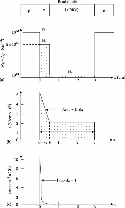
FIGURE 2.9
Read diode (a) doping profile (p-n-i-n), (b) ionized integrand at avalanche breakdown and (c) Avalanche region. (After Bhasin, K.P. et al., Monolithic optical integrated control circuitry for GaAs MMIC-based phased arrays, Proc. SPIE 578, September, 1985.).
This is because of the avalanche phenomena. Avalanche occurs when electron–hole pairs are created. These free carriers have enough energy that when they impact with other electrons, ionization occurs, creating even more free carriers. As long as the bias voltage across the diode is larger than the breakdown voltage, avalanche breakdown occurs; therefore, the maximum amount of avalanche current occurs at the time just before the bias dips below the breakdown voltage. This is referred to as the injection phase delay.
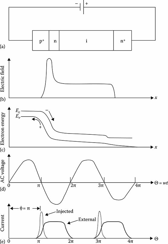
FIGURE 2.10
Read diode (a) p-n-#-n structure, (b) field at avalanche breakdown, (c) energy-band diagram, (d) AC voltage, and (e) injected and external currents (After Bhasin, K.P. et al., Monolithic optical integrated control circuitry for GaAs MMIC-based phased arrays, Proc. SPIE 578, September, 1985.).
The injection phase delay must be present for the IMPATT diode to exhibit negative resistance. This can be seen by looking at Figure 2.11 which is a plot of AC resistance at three different injection phase delays. Note that when there is no injection phase delay (Φ = π), the AC resistance never becomes negative. Therefore, no oscillation can occur when there is no injection phase delay. The maximum negative AC resistance then occurs when the AC voltage just starts into its negative half cycle. The injected carriers drift across the drift region of length W at their saturation velocity, vs, during the negative half cycle of the AC voltage. Therefore, the frequency of oscillation is f = vs/2W.
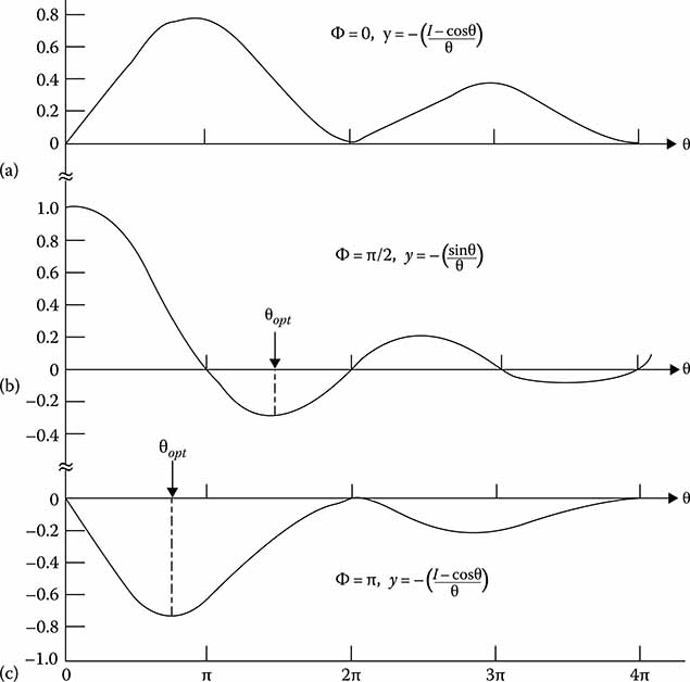
FIGURE 2.11
AC resistance versus transit angle for three different injection phase delays, (a) Φ = 0, (b) Φ = n2, (c) Φ = n
Several important characteristics of the microwave packages used for IMPATT oscillators are the cavity and the heat sink material at the base of the package. The cavity envelops the IMPATT diode, and its dimensions are such that oscillations at the correct frequency are obtained. The packaging material must have a relatively low coefficient of expansion relative to temperature in order to ensure proper oscillation over the specified temperature range. The heat sink material must be a good thermal conductor because of the heat buildup from the high electric fields present in the avalanche region that cause impact ionization current.
The IMPATT diode is the most powerful solid state device in the microwave and millimeter wave regions. Pulsed outputs of >30 W have been achieved at 10 GHz. Output power approaching 10 W has been seen at a frequency of >100 GHz. The efficiency of the IMPATT diode has reached as high as 37% in a pulsed operational mode. The aforementioned IMPATT diode characteristics make it an important device for the future and a logical choice for optical control.
2.2.3.2 Illumination Effect on IMPATT Diode Operation
Many effects on IMPATT diode behavior due to optical control have been investigated [26]. This section will cover four of the most important effects on performance. These are frequency tuning or shifting, noise reduction, AM/FM modulation of the oscillating frequency, and injection locking of the IMPATT, which is a “cleaner” signal.
Frequency tuning is a very important capability for oscillators. Not only can the frequency be shifted by illuminating the IMPATT diode, but the shifting can be accomplished much more quickly than by conventional control techniques. Noise reduction is important in any frequency-generating system because the lower the noise, the more sensitive a system will be to small offsets of frequency such as in a Doppler radar or a coherent receiver system. Also, noise reduction is important since present frequency spectrums are already overloaded. By reducing the noise output of an oscillator, the interference with other systems operating on nearby frequencies will be reduced. AM/FM modulation of the IMPATT is very useful when using the IMPATT as an oscillator in a communications system, because now the diode can be modulated by a light source in order to transmit information from one point to another. Also, because the light source is usually a laser, the modulation frequency can be expected to go high in the future due to the constant improvements in laser technology. Finally, injection locking of the IMPATT diode using optical techniques is very promising because of the capability to control the frequency of one or more frequency sources. This is very beneficial when utilizing IMPATTs in a system where coherent sources are necessary as in Doppler radars.
2.2.3.3 Experimental Results on IMPATT Diodes: Optical Tuning
Optical tuning is achieved by illuminating the IMPATT diode by a laser source. Photogeneration of carriers occurs that alters the timing of the avalanche cycle. This alteration in avalanche injection phase produces a change in the oscillation frequency of the diode. These changes in frequency can occur more quickly than by conventional means of control.
Data from one particular experiment will now be discussed [27]. This experiment is singled out because the IMPATT diode had an operating frequency of about 92 GHz. Most previous experimentation on optical control had been done on IMPATTs that operated below 18 GHz.
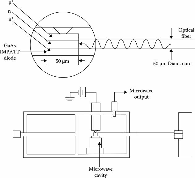
FIGURE 2.12
Optically synchronized microwave oscillator.
In this experiment, the p+-n-n+ diode was illuminated by a GaAs/GaAlAs laser operating at 850 nm. Figure 2.12 shows the basic method used to illuminate the IMPATT diode. The output frequency was first measured with the free-running oscillator. The frequency was 91.83 GHz with a bias current of 100 mA. The diode was then illuminated with 3 mW of laser power that optically generated 20.5 μA of current. This resulted in a 9 MHz shift in frequency. Less than 10 MHz frequency shift was achieved because of the poor coupling between the laser and the IMPATT diode. If the coupling efficiency was improved to the point that typical high-speed photodiodes have performed, a frequency shift of 600 MHz could be obtained.
In addition to the tuning range, tuning speed is another important parameter. Ninety percent of the 9.4 MHz frequency change occurred in 55 ps, or just <20,000 changes in frequency in about 1 μs. Optical control certainly allows fast response.
2.2.3.4 Noise Reduction by Optical Means
One source of noise in an IMPATT device is the noise generated during the avalanche multiplication process [28]. This noise is due to the variation in successive cycles of the injected avalanche current. This variation is due to the small amount of carriers present during the start-up of the avalanche cycle that leads to jitter in the avalanche cycle. This causes high oscillator noise levels. By increasing the reverse saturation current in the IMPATT, noise can be reduced. Optical illumination can be used to increase the reverse saturation current by photogenerating carriers in the diode.
Experiments were performed on both Si and GaAs IMPATT diodes. The Si oscillator had an RF output power of 260 mW at 10.47 GHz, and the GaAs oscillator power was 420 mW at 10.44 GHz. Both diodes were illuminated with a HeNe laser at 632.8 nm. The FM noise output from 0 to 50 kHz offset was measured for both diodes.
At very low illumination levels, no improvement in noise performance was measured. This is because the optically produced current is much less than the thermally generated saturation current that is greater for Si than for GaAs since the bandgap for Si is less than that for GaAs.
Increasing the illumination resulted in a decreasing FM noise level. The GaAs diode showed a 5 dB improvement in carrier/noise level at <7.5 kHz offset from carrier. The Si diode showed only a 2 dB improvement at <7.5 kHz offset because of the greater reverse saturation current already present in the Si diode. Results from this experiment also showed that if laser sources with greater amplitude stability were available, the noise performance of the IMPATT diode could be improved even further.
2.2.3.5 Optically Induced AM/FM Modulation
Optically illumination can be used to modulate an IMPATT oscillator [29]. AM modulation can be attained by two methods—quenching or enhancing. Quenching occurs when illumination of the diode alters the Q factor of the oscillator circuit enough to stop all oscillations of the diode. Enhancement of the oscillator output can occur with illumination of the diode, but only within a limited optical power range; therefore, quenching is the dominant effect used to AM modulate an IMPATT diode oscillator. FM modulation is produced by the change in susceptance of the device due to optical illumination. This change in susceptance leads to significant shifts in frequency.
Experimental results on X-band silicon IMPATT diodes that were modulated by optical means will now be discussed. The laser used was a 10 W 900 nm GaAlAs source. The laser was pulsed for 0.1 μs at a repetition rate of 200 Hz. AM modulation was observed in both the quenched and the enhancement modes. In the quenched mode, the ratio of RF power during laser-on and laser-off states was about 10 dB. A total of 20 dB was obtained in the enhancement mode; however, AM modulation in the enhancement mode is much more difficult to implement. FM modulation was also observed. Frequency deviations of >4% were seen. Greater deviation could be reached at the expense of excessive AM modulation.
2.2.3.6 Optical Injection Locking
Optical injection locking is the technique whereby the IMPATT frequency is controlled by a purer microwave source [30]. This technique is useful when many IMPATTs must operate in a coherent fashion. Optical injection locking has a very promising future in the fields of radar and communications.
There are two types of optical injection locking. One is direct injection locking and the other is indirect injection locking. Direct injection is illustrated in Figure 2.13. A laser is used to illuminate the IMPATT diode that is encased in a microwave cavity. Along the way, the laser light is intensity modulated by a microwave source feeding an electro-optic modulator. This intensity modulation triggers the avalanche process, thereby controlling the frequency of oscillation of the IMPATT. This is referred to as the direct injection locking method because the optical signal is directly illuminating the IMPATT. Indirect injection locking is shown in Figure 2.14. Note the difference between direct and indirect locking. Indirect locking the optical signal, which is modulated by the master oscillator, does not reach the IMPATT diode at all. The modulated optical signal controls an intermediate device that then electrically controls the IMPATT. In Figure 2.14, the intermediate device is the PIN diode.
Another difference between methods of injection locking is whether the fundamental frequency of the IMPATT is used as the cleaner microwave source frequency or whether a subharmonic of the IMPATT frequency is used as the microwave source frequency. For example, in Figure 2.13 [31], if the IMPATT frequency is 10 GHz and the microwave frequency into the electro-optic modulator is 10 GHz, then fundamental frequency locking is occurring. However, if the IMPATT frequency is 10 GHz and the microwave source frequency is some subharmonic of the IMPATT, say 5 GHz, then subharmonic locking is occurring. Subharmonic locking is advantageous over fundamental locking, especially in higher IMPATT frequency applications, because lower frequency microwave sources can be used that results in cost savings.
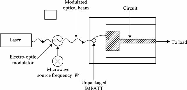
FIGURE 2.13
Optical synchronized microwave oscillator.
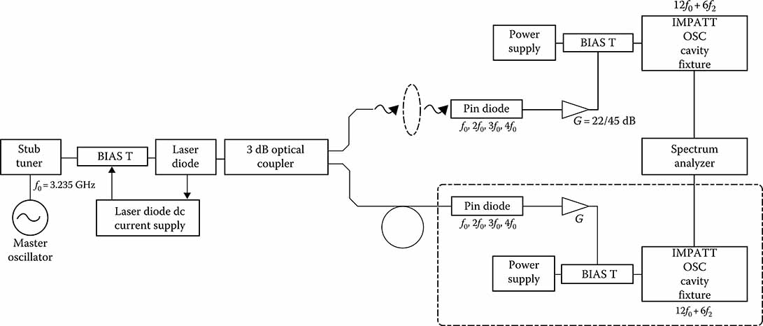
FIGURE 2.14
Experimental setup for indirect optical injection locking of 2 mm wave IMPATT oscillators. The dotted enclosed section is not presently used.
Experimental results of a 38.82 GHz silicon IMPATT oscillator using indirect subharmonic injection locking will now be discussed. Figure 2.14 shows the experimental setup. The master oscillator frequency is 3.235 GHz. This frequency modulates the drive current to the laser that results in the laser, being intensity modulated at the same frequency. The output power of the laser is 10 mW and it operates at a wavelength of 830 nm. The modulated laser output is split and the two laser signals control the PIN photodetectors. The fourth harmonic of the master oscillator, 12.94 GHz, is generated by the PIN photodetectors and is amplified by variable gain amplifiers. This fourth harmonic is electrically injected into the IMPATT and injection locking at 38.82 GHz, the third harmonic of 12.94 GHz, occurs.
Results of the experiment are encouraging. FM noise performance improvement of the injection locked IMPATT versus the free-running IMPATT is significant. The free-running IMPATT FM noise was −50 dBc at 100 kHz offset from carrier. Once the IMPATTs were injection locked, the FM noise was −55 dBc at 5 kHz offset from carrier. Locking range of the IMPATT was also evaluated. When the amplifier following the PIN photodetector had a gain of 22 dB, a locking range of 2 MHz was observed. With an amplifier gain of 45 dB, the locking range was 132 MHz. These results indicate that indirect injection locking could be used to apply FM to the master oscillator in order to use the IMPATT in a communication or radar system.
2.2.4 TRAPATT Oscillators
TRAPATT stands for TRApped Plasma Avalanche Triggered Transit. Oscillators using TRAPATT diodes have higher power and high-efficiency capability [32]. Pulsed outputs of up to 1.2 kW at 1.1 GHz and efficiencies of 75% at 0.6 GHz have been observed. Operating frequencies are limited to the microwave frequencies and below.
Diode structures can be either n+-p-p+ or p+-n-n+. The basic theory of operation is as follows. Upon application of a current step function to the diode, an electric field will be established that decreases linearly with distance from the injected current. The electric field will increase until the critical field, Em, is reached. This critical field will move across the diode causing avalanche breakdown. The velocity with which the avalanche zone sweeps across the diode is very high-higher than the saturation velocity of the newly created free carriers. This leaves the diode filled with a plasma of free carriers. This plasma now travels across the diode, but at very low velocity due to the voltage across the diode dropping significantly after the avalanche zone passes. Because of the low velocity of the free carriers, the transit time across the diode can be much longer than if they were traveling at the saturation velocity. This transit time delay provides the needed phase delay for oscillation. Because the transit time is relatively long, the frequency of operation can be quite low compared with the IMPATT diode.
2.2.4.1 Illumination Effect on TRAPATT Operation
Three effects of illumination on TRAPATT diodes will now be discussed. These are not the only effects observed, but are effects that have real system applications. The effects are reduction of startup jitter, frequency shifting, and variation of RF power output [33].
2.2.4.2 Experimental Results: Start-Up Jitter Reduction
Start-up jitter in TRAPATT oscillators can be very troublesome. Jitter on the order of 100 ns is common and this becomes even worse with temperature. Optical injection of carriers into the diode during the low-current portion of the RF cycle can stabilize the TRAPATT mode and thus reduce start-up jitter.
Experiments on a silicon TRAPATT diode operating at 700 MHz with a power output of 70 W continuous were performed. Illumination was provided by a GaAs laser diode operating at 904 nm. Without illumination, the TRAPATT displayed about 100 ns of start-up jitter. When the TRAPATT was illuminated by a laser pulse positioned in time at the leading edge of the TRAPATT bias pulse, reduction in jitter occurred. Reduction to as low as 30 ns was observed with a laser output of 0.2 W/cm2. This reduction in jitter was also made less temperature dependent.
2.2.4.3 Frequency Shifting
Experimental results on a silicon TRAPATT diode will now be discussed. Optical control of the frequency was noticed with laser illumination at levels greater than 10−2 W/cm2 from a GaAs laser operating at 904 nm. The TRAPATT, whose frequency range was from 654 to 1493 MHz, could be shifted in frequency by about 1% at the low end of the band and by about 7% at the highest frequency when stimulated by the laser. In most cases, as the illumination level increased, so did the TRAPATT frequency.
2.2.4.4 Variation of Output Power
Using the same setup as in the previous discussion on frequency shifting, the power level of the TRAPATT could be controlled. The effect of the illumination depends on the frequency of oscillation of the TRAPATT. At the low end of the frequency band, the power lever decreases with increasing illumination, whereas at the higher frequencies, the power level increases with increasing power level. Power variation of about 9 dB was achieved when the illumination varied from 10−2 to 1000 W/cm2.
2.2.5 MESFET Oscillator
An experiment on a MESFET oscillator was carried out to determine the capability to optically injection lock the oscillator [34]. This experiment was spurred by previous work on MESFETs which showed that the oscillator frequency could be tuned by varying the illumination intensity striking the active region of the MESFET. The illumination creates free carriers in the channel region that alters the DC characteristics of the device.
The MESFET was controlled by a GaAs/GaAlAs laser that produced an output power of 1.5 mW at 850 nm. The laser was modulated by a klystron oscillator that could be tuned around the MESFET oscillator frequency at about 2.35 GHz. Comparisons of the FM noise level of the free-running oscillator and the oscillator locked to the klystron were made. Measured in a 1 Hz bandwidth, the RMS FM noise deviation was only a few hertz at 10 kHz offset from the carrier. This is a significant reduction in the noise spectrum of the oscillator.
Locking range of the MESFET oscillator was also examined. A maximum locking range of 5 MHz was obtained. A greater locking range could be achieved if more efficient coupling existed between the laser and the FET chip, and also if more of the microwave signal could be coupled to the laser.
2.2.6 Transistor Oscillators
Transistors can be optically controlled by illuminating the base region with a light source. The light source generates carriers in the base that affect the conductivity of the transistor. In other words, the light source acts as an additional supplier of base current.
Experimental results on optically injection locking a transistor oscillator will be reviewed [35]. A silicon transistor with its lid partially removed to allow illumination was used. The illuminating device was GaAlAs laser operating at 820 nm. The laser output was intensity modulated by a signal generator with a frequency of 110 MHz. The frequency out of the transistor oscillator was 330 MHz which demonstrated that subharmonic optical injection locking took place. Fundamental frequency locking may also occur. The locking range of the oscillator was limited due to the same reasons discussed previously. First, the modulation method of the laser was inefficient; second, the coupling efficiency of the laser light into the transistor base region was low.
2.2.7 Optical Control of Passive Devices: Dielectric Resonator Oscillator
The DRO is used more readily as its benefits are realized. Some of the advantages of the DRO over other oscillators are reduced phase noise, higher efficiency, and lower susceptibility to microphonics. Figure 2.15 shows a simple depiction of a DRO circuit. Notice that the dielectric resonator is placed in close proximity to the output stripline that affects the feedback characteristics of the FET oscillator. The resonator couples magnetically to the feedback path and the distance between the resonator and the microstrip line determines the amount of coupling.
Optical control can be achieved by adding a photoconductive sample on top of the dielectric resonator material. Once illuminated, the conductivity of the photoconductor increases that alters the magnetic coupling of the dielectric resonator resulting in a frequency shift of the DRO.
2.2.7.1 Illumination Effects on Dielectric Resonator Oscillator
Two effects of illumination on DROs are discussed. First, frequency tuning, or shifting, is reviewed as with the IMPATT and TRAPATT diodes. Also, FM modulation of the DRO is discussed. Experimental results on other illumination induced effects are still in development.
2.2.7.2 Experimental Results: Optical Tuning
Experiments were performed on a 10.2 GHz DRO. Illumination was provided by three sources: white light, a HeNe laser with a power output of 5 mW at 630 nm, and a GaAs LED with a power output of 1 mW at 850 nm. The white light source shifted the DRO center frequency by 5 MHz and also lowered the power by 1 dB. A total of 1 W/cm2 of light output power was used. A 0.4 MHz frequency shift was obtained using the HeNe laser, and a 0.5 MHz shift was seen with the GaAs LED. In addition to a constant intensity illumination, the light sources were varied in intensity to determine their effect on frequency shift. Results showed a linear relationship between frequency shift and light intensity as shown in Figure 2.16 [36].
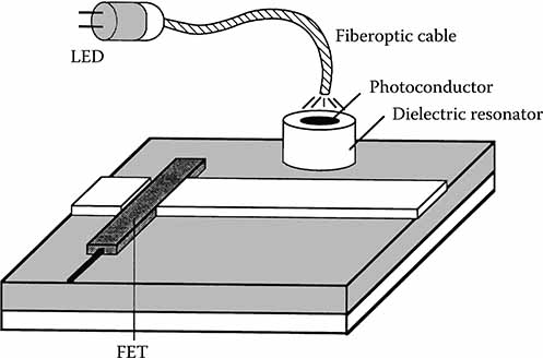
FIGURE 2.15
Optical tuning of the dielectric resonator.
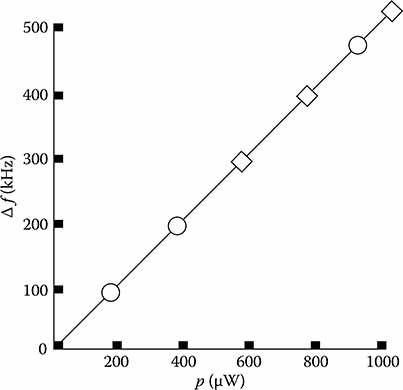
FIGURE 2.16
Shift in the DRO resonant frequency as a function of IA LED output power.
2.2.7.3 FM Modulation
FM modulation experiments were performed using an AM-modulated LED as the coupling mechanism to the photosensitive sample. Modulation rates of 130 MHz were observed; however, higher rates could have been achieved if the LED would not have limited the rate.
2.2.8 Applications of Optical Control
Applications of devices controlled by optical means are diverse and constantly increasing. A description of some common applications provides a better understanding of why much of the research has taken place.
One very important area for utilization optically controlled devices is in phased array radar systems. Phased arrays radars have many emitting elements (sometimes >10,000) on a planar surface. These emitting elements allow the antenna pattern to be electrically steered very quickly but, in order for the pattern to be correct, the phase and frequency of each one of the elements must be controlled rather precisely. In the past, these elements, which are actually oscillators, were controlled electrically either by coaxial cable or by waveguide. Because of the weight, volume, and expense involved in running >10,000 waveguides to a phased array radar, many radars that could have been phased array in the past were implemented in some other fashion. With optically controlled oscillators, however, these radars can now be implemented as phase arrays, because the control signal to each oscillator can be fed through small, lightweight, and inexpensive fiberoptic cable. Thousands of oscillators can be injection locked by a single master oscillator whose output is modulating a laser. Megawatts of output power can be achieved if IMPATT or TRAPATT diode oscillators are used. Millimeter wave operation is quite feasible.
Another radar application using optically controlled devices is in Doppler type radars. Depending on the frequency of radar operation and the velocity of the expected targets, the Doppler return could be very close to carrier frequency. Doppler offsets of 1 Hz are commonplace. In order for the Doppler to be detected, the system must be coherent in frequency and phase, and the noise level close to the carrier must be relatively low. Using the optical technique described in the IMPATT section, one could optically injection lock several oscillators in a system that would maintain frequency and reduce phase noise.
High-resolution radar applications could benefit from optically controlled devices. With the shorter pulse durations and the reduction in leading edge jitter (start-up jitter) afforded by optical control, the ambiguity in target range is reduced dramatically.
Frequency agile communications and radar systems are also candidates for optically controlled devices. The faster a system can “hop” from one frequency to another, the better. Subnanosecond frequency switching times exhibited by the optically controlled IMPATT diode oscillator mentioned earlier would be ideal.
Systems requiring immunity to EMI could use optical technology. Shipboard systems, for example, have to withstand extreme EMI environments because of the radar and communication gear on board. Since the optical signal would run through fiber-optic cable, the control signal would be inherently immune to outside EMI. Also, if there is information being transmitted through the cable that must be protected, the information is more secure than with electrical conductors.
Still another application is in airborne or portable systems where size and weight must be kept to a minimum. Using fiber cable reduces both of these critical parameters and also allows more complicated systems not possible without optical control. Finally, laboratory test setups are in need of devices and systems that are optically controlled. Laboratory work usually involves more precise control of parameters than in fielded systems. Narrower pulses and faster tuning can be achieved with optical control.
2.2.9 Future Needs and Trends
The future requirements of electronic systems warranting the use of optically controlled devices are many. Optical control promises to solve many of the current limitations of electronic systems. One of these is the need for faster switching devices. Switching speed improvements are required for on/ off, frequency, and power level switching. Wider bandwidth systems are also needed to improve the locking range of injection locked systems. Improving the locking system will allow even more modulation of the carrier frequencies. With this comes wider bandwidth capability and the requirement for higher modulation rates.
Another requirement will be to control electronics with less optical signal power. Currently, the coupling efficiency between the light source and the microwave device is very poor. Higher reliability and producibility requirements will follow the successful laboratory demonstrations of new concepts. Size and weight reduction will be stressed.
One key trend is the fabrication of optical and microwave components on a single monolithic device. As discussed in Section 5.11, much of the MMIC technology can be directly applied to the development of optics modules. Optomicrowave monolithic integrated circuits will assist in obtaining better control of the microwave devices with less optical power because the coupling efficiency will increase. Size, weight, reliability, and manufacturability will ultimately improve with the OMMIC systems as well. Laser technology will also continue to improve on the current limitations of optical control. Higher modulation rates and noise reduction improvement will parallel the improvements in laser technology.
2.3 Lithium Niobate Devices
A large number of important devices that are fabricated in LiNbO3 have been discussed in the literature. Some of the most interesting of these are described in this section [37].
2.3.1 Optical Switches
One of the most important LiNbO3 devices is the optical switching device. Response times as fast as 1 ps are possible [38] due to the electro-optic effect inherent in lithium niobate, so that high-speed switching is limited merely by the circuit delays that result from the finite length of these devices. The fundamental building block of any optical switching network is the simple changeover point or 2 × 2 optical cross point shown in Figure 2.17 [39]. In the through state ports, 1 and 3 and 2 and 4 are connected. In the crossed state, 1 is connected to 4 and 2 is connected to 3. This crossed state may be achieved by mechanical means such as by physically moving the fiber or a prism into the optical path. If the waveguide is made from a material such as LiNbO3, however, then the crossing may be caused by applying a voltage and utilizing the electro-optic effect. The latter is obviously preferred due to difficulties in aligning microfibers, prisms, etc., in a mechanical setup. Currently, typical LiNbO3 switches have insertion losses of 3–5 dB, extinction ratios of 20–30 dB, and require control voltages of 2–30 V depending on switching speed. For mechanical microoptic devices, these values would be 1.5 dB, >60 dB, and 14 V, respectively [40]. The cost of each type of device is roughly the same; however, LiNbO3 switches are rapidly evolving, and improved device performance as well as greater reliability and lower cost will push the balance in favor of that technology.
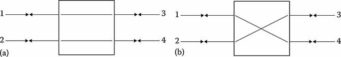
FIGURE 2.17
(a) Simple changeover point and (b) 2 × 2 optical cross point.
2.3.2 Directional Couplers
The basic directional coupler shown in Figure 2.18 [41] consists of two identical single-mode channel waveguides fabricated in close proximity via Ti diffusion over a length L. This allows synchronous coupling between the overlapping evanescent mode tails. Typical values of L are on the order of 1–10 mm. If the velocity of propagation is the same in both guides (same refractive index), then the light will be entirely coupled into the second guide after a characteristic length referred to as the coupling length. This coupling length value is definable in terms of wavelength, mode confinement, and interwaveguide separation [42]. If the indices of refraction of the two guides are slightly different, the net coupling may be quite small, so that application of a voltage across the electrodes shown in Figure 2.18 will change the indices of refraction and, therefore, the propagation velocities, thus destroying the phase matching. This determines which port (3 or 4 in Figure 2.18) the light will be coupled into after a length L. For directional couplers, switching speeds as fast as 1 ps are possible; however, to accomplish this device, lengths must be on the order of 1 mm. Although not a fabrication problem it is known that the shorter the device length, the greater the applied voltage must be in order to obtain optical isolation [43]. For device lengths of 10 mm, control voltages of 2–8 V are required dependent on the wavelength. For 1 mm devices, voltages of 10–30 V are required. Two other examples of directional couplers are the X switch and the merged directional coupler (Figures 2.19 and 2.20) [44]. Again a applied voltage will cause a change in refractive index to occur causing changes in the coupling ratio. Switching characteristics are direct functions of device length and switching voltage as with previous devices.
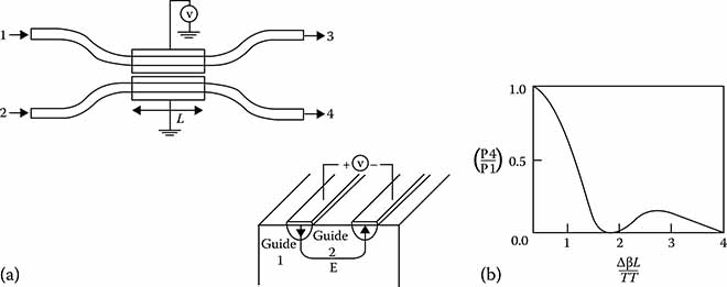
FIGURE 2.18
(a) Directional coupler and (b) transfer characteristic.
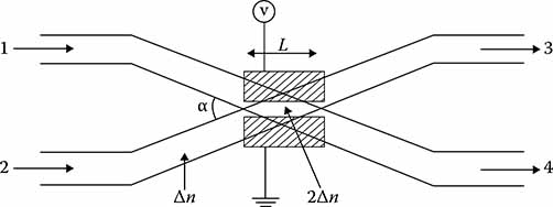
FIGURE 2.19
X-switch.

FIGURE 2.20
Y junction switch.
2.3.3 Modulators
Two important interference type waveguide modulators are Crossed-Nichol and the Mach Zehnder devices shown in Figures 2.21 and 2.22 [45]. In the Crossed-Nichol architecture, metal electrodes are formed on the crystal surface adjacent to the waveguide. The input beam is then divided into two components (TE and TM propagating mode) and due to the material birefringence, the separate components will be phase modulated differently as a voltage is applied to the electrodes. In the Mach Zehnder type, the input beam is divided into two identical interferometer arms. These arms may be thought of as two phase modulators and the applied voltage may be adjusted, so that the signals are either in or out of phase on recombination. The voltage required for a phase shift is [46]
Vx=λg2δn3er33Le(2.3)
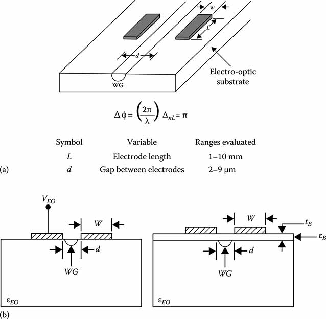
FIGURE 2.21
(a) The guided-wave phase modulator layout and (b) basic guided-wave phase modulator surface electrode architectures.
FIGURE 2.22
Schematic representation of modulator structure.
where
λ is the wavelength
g is the gap between the electrodes
δ is the electric/optical field overlap factor
ne is the extraordinary refractive index
r33 is the material electro-optic coefficient
Le is the length
If out of phase, the signal no longer propagates along the waveguide and radiates away into the LiNbO3 crystal. If in phase, the light remains in the guided mode and continues to be transmitted through the device. The intensity-modulated outputs are
l=l0sin2(Δϕ2)Crossed - Nichoal(2.4)
l=l0cos2(Δϕ2)MachZehnder(2.5)
where l0 = input light intensity. Mach Zehnder type devices generally provide up to 3× the efficiency of the Crossed-Nichol devices.
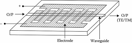
FIGURE 2.23
Polarization TE-TM modulator/converter.
2.3.4 Polarization Controllers
Another important device is the polarization controller (Figure 2.23) [47]. In these devices, two interdigitized electrode fingers are formed over a single waveguide. The electrodes affect the two components of the general elliptical polarization state (TE and TM) modes by modifying their relative amplitudes and phases. The voltage in the interdigitized section of the electrode changes the relative polarization amplitudes of the modes, while the voltage in the uniform portion acts to change the relative phases of the modes. Effective coupling between these orthogonal modes may be achieved with conversion efficiencies better than 99% [48], with an applied voltage of 13 V and an electrode period of 7 μm. The phase matching condition is [49]
2(πλ)(NTE-NTM)=2πΛ(2.6)
where
Λ is the electrode period
NTE and NTM are the effective waveguide indices
2.3.5 Integrated Systems
Several other device types exist such as Bragg effect modulators (Figure 2.24), frequency translators [50], and tunable wavelength selectors. These all operate in similar fashion to those devices already described. Although any of these devices may be separately fabricated and then assembled into packages via single-mode splices or connectors, this approach is simply not practical. This is because the insertion losses and the system costs would be excessive, especially for systems requiring a large number of components. These systems can be made practical via the integration of several components onto a single substrate. Examples of such integrated devices that have been fabricated include: a coherent optical receiver (Figure 2.25) [51] and directional couplers (Figure 2.26) [52]. The only limit to integration arises from the required device lengths since the cell sizes for integrated optical devices are quite large relative to electrical integrated circuits. Device lengths of several millimeters are required if high modulation rates are to be achieved. Device widths are less, however, and there is a great potential for arrays of identical devices to be fabricated onto a single crystal of LiNbO3 with parallel inputs. At this time, the best lightwave system performance of 8 Gbs/s over an unrepeatered distance of 68 km [53] is achieved via the use of Ti:LiNbO3 devices. As the technology matures, these devices are expected to play a critical role in future optical signal communications.
FIGURE 2.24
Bragg-effect electro-optic modulator.
2.4 Applications of Fiber-Optic Systems
Fiber-optic transmission is utilized in data communications and telecommunications for local area networks and telephone trunks. Video transmission, closed circuit television, cable television, and electronic news gathering utilize fiber optics, while in the military, command, control, and communications and tactical field communication systems are being developed and installed with fiber links. Optical circuits are applicable in each of these applications as interconnecting components in the system. Active devices such as sources and detectors are utilized in transmitters and receivers, and a number of passive devices perform various critical functions in the fiber-optic system. These functions include switching and routing, modulation, regeneration, processing, sensing, and multiplexing. Devices include taps, distributors, couplers, concentrators, switches, relays, multiplexers (MUXs), cross connection cabinets, and gratings. Local area network topologies currently in use as well as those in the development stages require a number of devices for the most efficient operation. A growing trend is toward all-optical switching systems, eliminating the use of slower electrical routing of information.
When comparing the performance of fiber transmission media to the alternative electrical twisted pair or coaxial cable conductor, the ability to utilize the wider bandwidth of the fiber without an increase in attenuation is a clear advantage. In addition, significant size reductions and greater resistance to long-term environmental degradation provide advantages to the fiber medium.
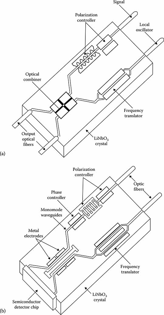
FIGURE 2.25
(a) Z-cut LiNbO3-integrated optic coherent receiver device. (b) X-cut LiNbO3-integrated receiver device.
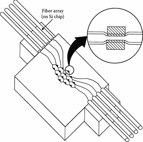
FIGURE 2.26
Diagram of a 4 × 4 directional coupler switch matrix.
2.5 Optical Interconnects for Large-Scale Integrated Circuits and Fiber Transmission Systems
2.5.1 Introduction
The limitations of conventional interconnects and switching technology are rapidly becoming critical issues in the throughput of data within the high-speed signal processors using LSI chips or GaAs-integrated circuits. The problems associated with transmission of Gb/s data must be addressed when designing integrated systems utilizing electrical interconnects and conventional switching technology. The performance of electrical interconnects at high data rates is adversely affected by increases in capacitance and reflections due to impedance mismatches. Optical interconnect technology promises to significantly enhance signal processing systems and provide relief from pinout, physical proximity, and clocking problems [54]. Furthermore, by releasing the bandwidth constraints imposed by electrical interconnects, the full processing capability of LSI chips could be exploited to improve currently fielded systems. Practical interconnection at the intraboard, backplane, and cabinet levels of signal processor system can now be realized with optical interconnects.
Faster logic switching times and increased use of very large-scale integration technology are placing new demands on digital system interconnections. In particular, board and backplane interconnect designs for future systems must satisfy requirements for increased density and improve electrical performance with respect to transmission of high-frequency signals. System parameters such as rise time, impedance level, and the assignment of ground return paths will have a significant effect on the high-frequency performance of electrical interconnections.
In order to realize the potential of the new families of fast switching components, there is an increasing need for system electrical interconnections to be designed as networks of transmission lines. Logic switching times continue to decrease at a much faster rate than the length of typical interconnections on the board or backplane level [55].
Interconnects may be classified by three categories according to their system-level utilization. These categories may be termed intraboard, backplane, and cabinet levels. The primary distinguishing characteristic of these categories is the interconnect length. Definitions of these lengths, albeit somewhat arbitrary ones, can be made. Intraboard level interconnects are approximately 5–15 cm long. Backplane level interconnects may run from 15 to 40 cm, while the longest interconnects are at the cabinet level and are typically on the order of meters.
2.5.2 Link Design and Packaging
The very large number of signal connections that must be made to densely integrated chips creates a very high density of separate conductors on the printed circuit boards. Multilayer boards relieve coupling and crossover problems by allowing crossovers to occur in different layers. These boards may be assembled as multilayered, multichip carriers that also contain metalized “vias” for vertical signal conduction. The number of chips and the dimensional extent of the modules is limited by the capacitance load that the chip is capable of driving without excess deterioration of rise time and/ or propagation delay. The use of special drivers or terminated transmission lines is not anticipated for these short internal connections.
One the other hand, the multilayer board structure does allow signal paths to be implemented in an approximation to the balanced stripline or the microstrip geometry; therefore, multilayer boards will permit terminated lines for point to point connections. Interspersal of signal lines between ground and power planes reduces crosstalk. Additional “shield” layers may be introduced while clock distribution on the boards can be accomplished with equal phase length-terminated branches. Various practical empirical rules have been determined for similar particular semiconductor technologies such as TTL compatible CMOS [56].
2.5.3 Backplane Interconnects
Backplane connections are proportionately long and the mutual inductive and capacitive coupling between conductors produce unwanted and intolerable crosstalk between circuits carrying fast rising signal waveforms. Backplane electrical design centers around minimizing and controlling these couplings. It is important that the couplings remain the same in successive copies of systems and not change during normal operation or servicing. To this end, orderly arrangement of printed circuit panels, ribbon cables, twisted pairs, and coaxial cables are used for these connections. Special interfacing line drivers are required for high-speed lines between chip modules.
Normally, a backplane structure is passive, serving only to supply interconnection and mechanical support. In some cases, active circuitry has been incorporated in the backplane presumably to reduce the lengths of some connections or to equalize lengths. This arrangement can create serious troubleshooting and maintenance problems however; and some systems made in this way are being retrofitted with passive backplanes.
2.5.4 Power Distribution
In multilayer modules, power distribution is accomplished by adding an additional layer to act as a power bus. By employing wide traces with minimum lengths, series inductance is minimized. In this manner, power busses can be considered as a line with low characteristic impedance.
A phenomenon that occurs in RF circuits and is detrimental in very fast digital circuits is the creation of relatively high Q resonators when the length dimension of the lines approaches a quarter or half wavelength of signal in the dielectric substrate. In some cases, the Q can be “spoiled” by introducing resistance across the bus at the ends.
Power distribution is a key determinant of a backplane’s performance and reliability. It is usually accomplished by heavy vertical bus bars. Before choosing a backplane configuration, the system’s current flows should be understood. Proper placement of inputs and returns ensures current densities will be uniform and voltage drops low enough to permit reliable operation. Paralleling connector pins at power entry points requires a significant derating of the current handling capability of the pins. Any small difference in contact resistance will significantly unbalance the current flows.
2.5.5 Large-Scale Integration Challenges
Many problems and issues remain to be resolved in the packaging and general usage of large-scale integration chips. The first of these issues concerns high-level interconnections among LSI components and devices. Although the development of LSI technology has been rapidly progressing, the only major interconnection issue that has been addressed has been at the chip-to-chip level. It is felt that a critical path in the incorporation of LSI components into various designs will be interfacing at the backplane and intercabinet levels. This will be particularly true for the interface speeds of LSI components.
The second issue is the actual insertion of LSI components into existing systems and the incorporation of these components into new product designs. The new problems of LSI electrical interconnects stem from two sources. First is the necessity to transmit high-speed data and clock signals over distances that are incompatible with the drive capabilities of the chips. Second is the lack of control of clock offsets between widely separated functional entities.
A prime consideration affecting communication between chips is the drive capabilities of the chips themselves. Additionally, these limitations do not allow the direct driving of any currently available optical sources. Analysis suggests that the critical length separating lumped element and transmission line considerations is on the order of 10 cm. This was obtained from calculations using a rise time of 7 ns as representative of typical 25 MHz chip signals.
A hierarchical approach to system implementation is envisioned wherein chips containing closely interacting functions or groups of functions are assembled in close spatial proximity as higher function modules. Combinations of superchip modules and line drivers should suffice for structuring circuits at the board level. The design goal is to minimize the number and length of high-speed transmission paths. Experience indicates the number of interconnections between assemblies decreases as one moves up through higher level assemblies. In the case of fewer high-speed channels traversing greater distances, higher power transmitters and more sophisticated receivers can be tolerated. Also, the requirement for synchronous clocking diminishes at higher assembly levels. At certain levels in signal processors, we move from intra- to intercomputer situations. These widely separated elements need to communicate over high-speed data connections—data connections that are impracticable given the chip drive capabilities.
2.5.6 Advantages of Optical Interconnects
There are a number of limitations of conventional interconnects that can be alleviated through the use of optical interconnects. The general advantage of optical interconnects over their electrical counterparts are the following:
Freedom from stray capacitance and impedance matching
Freedom from grounding problems
Provide relief from the pinout problem
Lower power requirements
Increased flexibility for interconnects
Light weight and small volume
Planar integration
Increased effective bandwidth of the system
Two-way communication over a single transmission path (fiber)
Passive MUX/DEMUX for high reliability at low cost
Major system cost reductions
Simple upgrading of existing systems
Immunity to RFI, EMI, and EMP effects
The first, and perhaps most important, advantage is the lack of stray capacitance. Optical interconnects suffer no such capacitance effects and crosstalk can be controlled as long as care is taken to avoid scattering effects in broadcast systems. The second advantage is freedom from capacitance loading effects. The speed of propagation of an electrical signal on a transmission line depends on the capacitance per unit length. As more and more components are attached to a transmission line, the time required to charge the line increases and the propagation speed of the signal decreases. Optical interconnects provide a constant signal speed (i.e., the speed of light in the guiding medium), which is independent of the attached components.
2.5.7 Compatible Source Technology
The telecommunications and optoelectronic industries have pursued extensive research programs investigating semiconductor optical sources operating at 0.85, 1.3, and 1.55 μm wavelengths. This has introduced to the marketplace a wide range of available sources that are capable of achieving previously unattainable modulation rates with extremely high reliability. LEDs are generally limited to hundreds of Mb/s up to 500 MHz [59]. In contrast, laser diodes, although similar in structure to LEDs, are highly efficient. An experimental InGaAsP laser has demonstrated an internal quantum efficiency approaching 100%. This cooled laser has also shown a bandwidth capability exceeding 26 GHz [60]. Depending on the system implementation used in the interconnection of LSI components, either of these types of sources would be adequate for data transmission.
High bit rate communication sources at high-speed pulse code modulation rates should have the following:
No modulation distortions (pattern effects)
Narrow spectral bandwidth
No high spectral broadening due to modulation
No self-pulsation (charge storage effects)
Currently at issue are the power requirements for both types of sources that range from 7 to 100 mA for adequate output in LEDs or threshold operation in laser diodes. The critical future laser requirements for the optimal usage of optical interconnections are “development of continuous wave room temperature frequency-selective lasers with high stability (10 Å) and low threshold current (5 ma)” [61] that are capable of being modulated in the tens of gigahertz just at or above threshold.
2.5.8 Receiver and Detector Technology
Optical interconnect receivers are basically high-speed optoelectronic transducers that receive incoming optical digital data, transform it to an electrical signal, amplify and filter it, and restore logic levels. There are several alternatives for detectors. Among these are p-i-n photodiodes, avalanche diodes, and Schottky barrier photodiodes. The p-i-n photodector is essentially a p-n junction with a controllable depletion region width—the “i” intrinsic region. Incoming photons generate electron–hole pairs in the intrinsic region and the carriers are swept out of the region by an applied electric field. The device speed is chiefly determined by the drift mobility. As a result, the fastest response times are achieved using GaAs devices. The voltage requirements to deplete the active region are on the order of 5–10 V.
The APD is also a p-n diode; however, it operates in a highly biased mode near avalanche breakdown. Its operation is similar to the operation of a photomultiplier tube with improved sensitivity of 3–10 dB. APD detectors can exhibit rise times in the 30–40 ps range and 80%–90% efficiency [62]. Schottky barrier photodiodes possess the advantage of being ideally suited for surface detection. They are constructed by using a thin, transparent layer of metal for one contact that allows the light to pass very efficiently into the semiconductor contact. With proper construction, any of these detectors are capable of detecting data rates in the gigahertz range and are compatible with the wavelengths and modulation rates of laser diodes and LEDs.
2.5.9 Integration of Sources and Detectors
Due to the telecommunications industry requirements, a large number of sources and detectors are available in single-device packages from commercial vendors. Space and power limitations become unacceptable, however, when considering these devices for use in smaller and faster computing environments. Such environments necessitate the development of lower power and high-density devices and packages [63]. In particular, packaging methods must be developed to allow high-speed silicon and GaAs components to be integrated with optoelectronic components and waveguides [64]. Direct integration of optoelectronic devices with conventional logic devices will increase density and reliability of the interconnect because the electrical–optical interface occurs on chip [65], eliminating the need for hybrid or separate packaging techniques for the optics.
If a photodetector is to be integrated on a circuit with more than a few electronic components, it must meet a number of criteria [66]. First, the detector must be compatible with electronics processing. It must therefore be processed on a production line and be compatible with the substrates used for the electronics. For GaAs, this means at least a 3 in. semi-insulating substrate. Second, the material for the detector cannot interfere with the electronics. Thus, if epitaxial material is required, it must be excluded from the regions in which the electronics will be fabricated and the transition to the epitaxial region must be smooth enough to permit fine-line photolithography. Third, any process needed to fabricate the detector cannot degrade the performance of the electronics. For example, a very high temperature step may cause unacceptable surface damage. Fourth, the detector and electronics must be adequately isolated on the substrate.
Finally, the integrated photodetector must meet the overall receiver system specifications. The receiver’s function is to convert the optical signal to an electrical signal compatible with digital electronics. This requires coupling the input fiber to the detector, designing and fabricating a detector with sufficient bandwidth and sensitivity, interfacing the detector with a preamplifier, and converting the analog signal from the preamplifier to a digital signal.
The sensitivity of the receiver depends strongly on the node capacitance, with the improvement being most significant for a reduction in capacitance at the highest bit rates. For example, a reduction in mean detectable optical power of nearly 5 dB is possible if the front-end capacitance is reduced from a relatively good hybrid receiver value of 1 F to a value of 0.2 pF at B = 1 Gb/s. This additional margin might then be used to permit a less-expensive coupling scheme or to power split from a laser to multiple detectors in an optical bus. Alternatively, the fivefold decrease in capacitance would permit the detector amplifier to be operated at nearly five times the bit rate with no degradation in accuracy. This is a strong argument for integration.
While the integration of the detector with the amplifier may prove to be the limiting factor on the speed of the optical link due to circuit limitations, the integration of the laser with associated electronics will be more difficult from a materials and processing compatibility standpoint. There are three reasons for this. Lasers require multilayered heterostructures up to 7 μm thick. They also need two parallel mirrors separated by on the order of 200 μm, and finally, a method for achieving electrical and optical confinement in the lateral dimension.
2.5.10 Integrated Device Developments
There have been a number of demonstrations of laser diodes integrated with either a single or a few GaAs IC components [67]. For the past several years, a number of companies, including Honeywell and Rockwell, have been developing technology to integrate optoelectronic devices with complex GaAs circuits [68]. One structure that has been demonstrated [69] is shown in Figure 2.27. The components in the structure are a transverse junction stripe (TJS) laser, a FET driver, and a 4:1 MUX. The MUX and driver active regions are formed by selective ion implantation into the semi-insulating GaAs substrate, while the TJS laser is fabricated by liquid phase epitaxial growth in a well etched into the substrate. The rear laser mirror facet is formed with a microcleave process developed at the California Institute of Technology, CA [70]. A cross-sectional view of the microcleave process is shown in Figure 2.28. The small horseshoe-shaped wing at the end of the laser is formed by chemically etching under the Al-facet. The wing is broken off to form a smooth cleaved mirror facet. Measurements have shown that lasers with undercut mirrors have operating characteristics (laser threshold 37 mA) identical to similar lasers having two cleaved mirrors. The optoelectronic chip having a size of 1.8 mm × 1.8 mm operated at speeds up to 150 MHz [71].
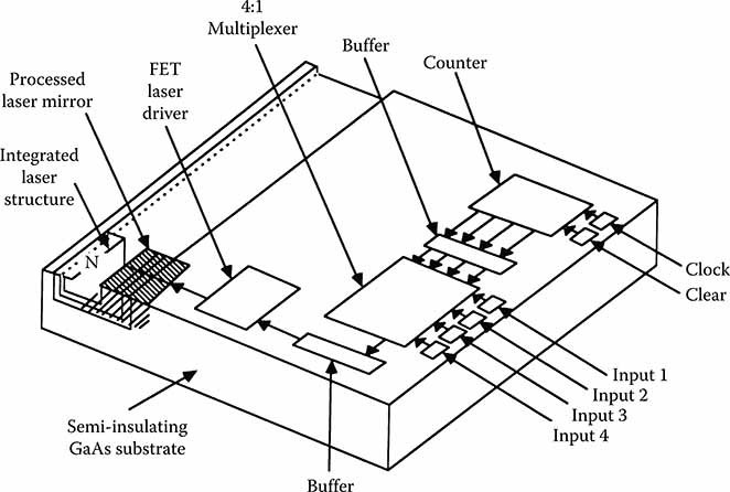
FIGURE 2.27
Block diagram of the monolithic optoelectronic transmitter consisting of an integratable TJS Laser, a laser driver, and a 4:1 MUX.
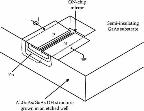
FIGURE 2.28
Schematic representation of the integratable TJS laser grown in an etched well. The on-chip mirror facet is formed by the undercut mirror process.
More recently, a 1 Gb/s optoelectronic receiver chip was demonstrated [72]. The receiver chip was designed to digitally multiplex four high-speed input signals. Two of the inputs are electrical and two are optical. The receiver consisted of two back-to-back Schottky diode detectors, two amplifiers, a 4:1 MUX, and a laser driver. All of the components were fabricated on a semi-insulating GaAs substrate using direct implantation MESFET technology.
The photodetector was fabricated on a semi-insulating substrate, thus eliminating the need for epitaxial growth. The pulse response of the back-to-back Schottky photodiodes [73] had rise and fall times for a range of bias voltages between −10 and −15 V of under 100 ps, which is sufficient for a 1 Gb/s operation of the receiver. The responsivity of the detector was measured to be 2.0 A/W for a wavelength of 0.84 μm. The output of the detector is fed into a three-stage amplifier, a preamplifier, a gain stage, and a buffer stage. The preamplifier translates the current into a voltage and amplifies to the proper GaAs logic levels by the gain stage, and the buffer stage is used as a line driver for the input of the 4:1 MUX. The preamplifier had a gain of 20 dB with a feedback around the second stage to improve its frequency response.
A similar effort on monolithic integration using a multiple quantum well (MQW) laser with a ridge channel waveguide structure [74] is shown in Figure 2.29. The MQW laser structure was grown by MOCVD and consisted of five 100 GaAs wells separated by four 40 Å Al0.2Ga0.8As barriers. The ridge waveguide was ion milled having a width of 5 μm. These integrated devices have shown room temperature operation with 15 mA thresholds and differential quantum efficiencies of 60%. For this particular integration scheme, the laser will be implemented as a surface emitter as shown in Figure 2.30. The laser light is coupled from the laser to a passive AlGaAs waveguide. The light in the waveguide is coupled from the surface either with an etched V-groove or a grating. This technique allows the user to fabricate lasers at any position on the chip rather than only at the edge of the chip. The method is more difficult to implement if fibers are to be used as the transmission medium; however, it does provide the flexibility for utilizing the third dimension and directing the optical signals via holographic techniques. The photodetector used in this development was a PIN structure grown by MOCVD. The device was a six-layer stack consisting of GaAs and AlGaAs layers. Initial tests on this device [75] have shown a dark current of <10 pA and a breakdown voltage of 80 V. A current gain of 10 was demonstrated at a voltage of 95% of breakdown.
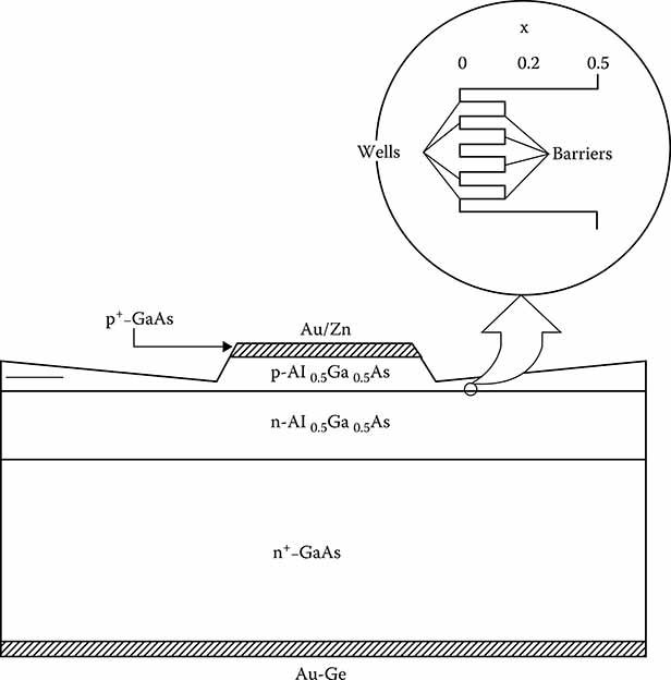
FIGURE 2.29
Cross-section and energy band diagram for ridge waveguide MQW laser.
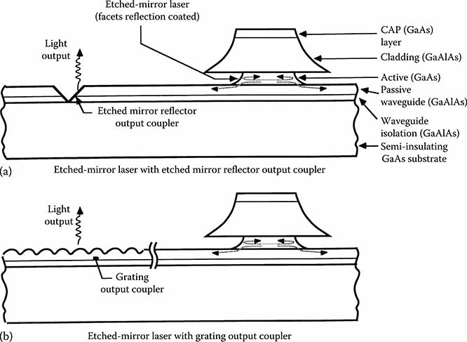
FIGURE 2.30
Surface-emitting laser using (a) etched V-groove and (b) grating.
2.6 Optical Interconnect Media
Optical interconnection of LSI chips requires a passive distribution network to transmit optical information from one point to another. To permit the general interconnection of one transmission point with other reception points in the system, the data are transmitted in a data packet from the various transmitters. As a result, the information is contained in a burst of bits, some of which indicate the destination, others the sender, and others the data to be transmitted. The nature of the transmission can be point to point or global. As a result, it is required that the optical interconnect medium permits efficient distribution of optical energy to all the required ports, with a minimal loss due to coupling and insertion loss of the optical signal. Furthermore, the dimensions of this optical medium must be compatible with the sizes of typical integrated circuits and systems utilizing such circuits.
2.6.1 Guided Wave Interconnects
The guiding of light for transmission via optical fibers is accomplished by confining the optical energy in a core region that is surrounded by a cladding layer of lesser refractive index. This refractive index profile from the core to the cladding generally takes two forms—either a sharp step function change (step-index) or a sharp change followed by a graded change (graded-index) in the core.
The two key differences between single- and multimode fibers are the dispersion characteristics and the dimensions. Dispersion causes signal degradation and therefore limits the distance over which transmission can be effectively accomplished. The dimensions of the guiding cores differ greatly between the two types of fibers causing ease of coupling and effectiveness of alignment to become issues.
Thin-film planar waveguides confine light using the same principle of differing refractive indices. In principle, the practical determining factors as to which materials can be used for waveguide fabrication are the refractive index, loss coefficient, and available dimensions. It is the last factor that promotes the use of thin films for the guides. For many acceptable materials, the refractive indices are such that the required waveguide dimensions are on the order of microns. Thin-film processing has advanced to the stage where films of this thickness are easily obtainable. Of special interest are waveguides in semiconductor materials. GaAs in particular has become increasingly attractive because of the compatibility with monolithic electronic and electro-optic device fabrication.
2.6.2 Single-Mode versus Multimode Fibers
Single-mode step index fibers possess the ultimate bandwidth capability due primarily to favorable dispersion characteristics. This means that single-mode fibers are the optimal choice for long haul applications in data transmission. In some applications, however, the lengths of transmission are such that multimode fiber can be utilized. A prime advantage of multimode fibers is the greater ease of coupling. Multimode fibers have acceptance areas of many orders of magnitude greater than single-mode fibers and thus have greater tolerance to misalignment and provide higher system gain.
Fiber dispersion can be classified as either intermodal or intramodal dispersion. Intermodal dispersion is found primarily in multimode fibers and is due to the differential delay between modes at a single frequency. This is eliminated in single-mode fiber since only one mode can propagate. Intramodal or chromatic dispersion is due to the variation of group velocity (the speed at which energy in a particular mode travels along the fiber) with wavelength.
For multimode graded-index fibers, the dominant cause of pulse spreading is intermodal dispersion. Experimentally determined values of this pulse dispersion have been found to range from 20 to 500 ps/km [76]. Dispersion values can be calculated exactly for quadratically graded index fibers. The results for calculations using an equation derived by Yariv [77] and particular fiber characteristics are shown in Figure 2.31. A reasonable bit rate for LSI applications would be 1.6 Gb/s. This assumes time division with sixty-four 25 MHz lines. The results of Figure 2.31 and the values quoted indicate that multimode graded-index fiber would be adequate to transmit over distances of approximately 20 m. With the use of single-mode fibers, the pulse spreading is due to group velocity dispersion. This dispersion, in turn, is dependent on the spectral width of the source.
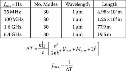
FIGURE 2.31
Quadratically graded index multimode fiber dispersion characteristics.
2.6.3 Broadcast Interconnects
The second technique for interconnecting various parts of high-speed integrated circuits involves the broadcast transmission of the optical signal in free space. Since substrates are planar, it can be envisioned that interconnection paths in free space must be perpendicular to the substrate plane to take advantage of the inherent three-dimensionality of free-space interconnects.
2.6.4 Free-Space Interconnects
With the free-space interconnect, the signal transmitted by the source is collimated by a lens or guided by a lens system. Detectors integrated into chips on the board receive the optical energy and convert it to electrical energy. The detectors can be made to receive the information with identical delays, due to the particular location of the source with respect to the focal point of the lens or mask. The system is highly inefficient, however, because only a small portion of the optical energy falls on the photosensitive areas of the chip. This method may therefore require additional amplification of the detected signal. This leads to increased power needs for boards, so that with many interconnects, this can be prohibitive in terms of heat dissipation and power requirements. Moreover, optical energy falling on areas of the chip where it is not wanted may induce stray electronic signals; therefore, it is necessary that opaque dielectric blockers be used. Openings in this layer would allow the detectors to receive the optical power.
2.6.5 Holographic Interconnects
Holographic interconnects fall into a class called free-space “focused” interconnects, which can also be called “imaging” interconnects. For such interconnections, the optical source is actually imaged by an optical element onto a multitude of detection sites simultaneously. The required optical element can be realized by means of a hologram that acts as a complex grating and lens to generate focused grating components at the desired locations. The efficiency of such a scheme can obviously exceed that of the unfocused case, provided the holographic optical elements have suitable efficiency. Using dichromated gelatin as a recoding material, efficiencies close to 100% can be achieved for a simple grating. The higher the number of focused spots, the lower the efficiency of available holographic methods. The flexibility of this method is excellent for any desired configuration of connections.
The chief disadvantage of the focused interconnect technique is the very high degree of alignment precision that must be established and maintained to assure that the focused spots are striking the appropriate locations on the chips. The spots can be intentionally defocused, with a trade between efficiency and alignment tolerance.
With holographic optical elements, a future possibility is the incorporation of dynamic holographic materials, such as those now being studied for four-wave mixing optical phase conjunction applications. Other future forms are banks of holographic mapping elements in conjunction with real-time masks. Candidates for such interconnections would be matrix-addressed liquid-crystal devices or the matrix-addressed spatial light modulator [78]. Another approach for a dynamic interconnect is the implementation of an optical matrix-vector multiplier [79].
2.6.6 Guided Wave versus Broadcast Interconnects
This represents the most critical trade-off decision as it determines the course of many others. Guided wave interconnects are inherently more efficient than broadcast interconnects. Since GaAs ICs will operate in the Gb/s range, the sensitivity of receivers is limited. As a result, the optical losses in the transmission of data from one board to another are limited to −27 dB for a signal-to-noise ratio of 100 (bit error rate = 1 × 10⁻¹⁰) [80]. Broadcast interconnection between devices on a board would require the use of large-area detectors and is not suitable for GaAs ICs. On the contrary, broadcast interconnects allow a large fanout of data, but guided wave interconnects also meet the needs of a large fanout with little or no loss occurring during transmission.
Optical fibers are currently the preferred choice. Owing to their flexibility, fibers can accommodate complicated topologies more readily than planar waveguides or broadcast methods. As mentioned, multimode fiber is more tolerant to misalignment than single-mode fibers, and is more tolerant than all other methods.
2.7 Multiplexing and Demultiplexing: Information Distribution Techniques: WDM Schemes
There are many advantages to wavelength division multiplexing (WDM) systems where lightwaves with different wavelengths, each carrying different information, are transmitted simultaneously through a single fiber. WDM data communication systems rely on the use of optical MUXs and DEMUXs designed to assure low insertion loss per wavelength channel, high isolation between channels, small size, and high reliability.
Several fundamental elements that have been considered for WDM applications are prisms, gratings, and interference filters, although other novel approaches exist. These components are the passive optical components that can perform the efficient multiplexing and demultiplexing of light sources into and out of trunk interconnections. In a data interconnect system, WDM is most advantageously utilized with optical fibers as opposed to other interconnection schemes.
2.7.1 Prisms
These MUX/DEMUX devices make use of the birefringement properties of various transparent materials. In general, this uses the principle of the dependence of optical speed in the material on wavelength. Two companies released representative product information on such devices [81]. GTE designed a two-channel system that can utilize source wavelengths that are 13–23 nm apart and have spectral widths of up to 6.5 nm. This is accomplished by using adjustable length polarizing prisms. The prism length is adjusted such that the two wavelengths emerge perpendicular to one another. ADC fiber optics offers both passive and active MUX/DEMUX devices. The passive device utilizes a biconical taper technique in which the coupling length of the device is wavelength dependent. Each wavelength, therefore, will exit at a different port of the device. The active device utilizes a dichroic filter to separate the different wavelengths. Although this type of filter is generally bulky, the ADC device is produced in a high-precision injection-molded plastic package that is small enough to be PC board compatible.
2.7.2 Gratings
In grating MUXs and DEMUXs, the mixture of wavelengths arriving in the transmission fiber or from the laser is separated and passed on to the receiver fibers. The light emerging from the transmission fiber or laser can be collimated by lenses before striking the grating. The angle at which the light is diffracted by the grating in relation to the optical axis depends on the wavelength. Several different gratings are currently available that have different diffraction efficiencies. One such MUX/DEMUX uses a chirped grating. This is an effective means of demultiplexing several channels, although gratings are somewhat bulky in comparison to integrated structures.
2.7.3 Bandpass Filters
In practice, bandpass filters, although functional in optical multiplexing, are a bulky WDM format. Several combinations of filters must be used depending on the number of channels multiplexed. Filter architectures could not be used for LSI board applications; however, some combination of WDM using a combination of two time division multiplexed (TDM) channels, where two channels are on different wavelengths, may be possible. It is not possible to wavelength multiplex a great number of channels using bandpass filters due to signal degradation encountered when passing through several filters. This is caused by the limited transmission ratio achievable with an interference filter. This ratio is 85% at best, although the maximum rejection of other wavelengths, determined by the reflection ratio, can be 100%.
2.7.4 TDM Schemes
TDM has important applications for LSI interconnects. When multiplexing a large number of signal channels, it is necessary to TDM to reduce interconnect complexity. Typical requirements are such that as many as 64 channels, each operating at 25 MHz, need to be transmitted. One possibility is to TDM the 16 bit address, data, and control words into four channels and then those four channels into one channel. This output channel would then be modulated at 1.6 GHz, which is entirely within the modulation rates attainable with laser diodes. Several commercially available GaAs universal shift regulators would meet the needs of this type of TDM.
2.8 Electro-Optic and Acousto-Optic Modulators
Electro-optic and acousto-optic modulators are the most highly developed types of modulators commercially available for digital communications. The drawback for these devices is that they operate in general on a power to bandwidth ratio of approximately 1 mW/MHz. The bandwidth of acoustooptic modulators is usually a small fraction of the acoustic frequency. This is highly prohibitive for data communications in the gigahertz band. The power requirements of these devices can also be prohibitive [82]. They are additionally quite bulky, although developments by some researchers to a rate above 1 Gb/s with order of magnitudes less drive power are available.
Electro-optic modulator response times are much more consistent with LSI data requirements. The electro-optic effect in certain materials is in the picosecond range and therefore does not limit the modulation bandwidth. The only limiting actors are the propagation times in the electro-optic crystals and the drive circuitry involved. For a modulator or reasonable drive voltage requirements, a bandwidth of approximately 2 GHz can be achieved at a wavelength of 0.633 μm in LiNbO3 [83]. This type of electro-optic modulator also compares favorably in its dimensionality. Thus, electronically addressed electro-optic modulators are very useful for modulation of continuous sources within LSI interconnect systems.
2.9 Assessment of Interconnect System Architectures: Optical Networking Architectures
Network concepts for interconnecting a large number of computing elements are numerous, including rings, banyan, Clos, Omega, Benes’, trees, spanning bus hypercubes, de Broijn, crossbar, gather scatter, cylinder, and other permutation networks. These networks must be compared to arrive at the most efficient network for interconnecting, given the ranges of data devices for a target application. “Efficient” in this context means not only the minimization of circuit complexity, delay, conflict at a node, synchronization, and coding, but also the ease of implementation in terms of optical interconnect technology.
There are several input issues that must be considered with high-speed optical interconnects. Many of these networks operate using burst-mode transmission. At very high-speeds, low levels of synchronization error or jitter are much more difficult to achieve if burst-mode transmission is used rather than synchronous operation. Jitter may be reduced by buffering, but at the cost of added network delay; therefore, synchronous operation is preferred to burst-mode transmission. Appropriate encoding schemes must be used for optical interconnects. Binary, balanced, and nonalphabetic codes are preferred.
2.9.1 Direct Relay Interconnects
The most direct method of interconnecting ICs from board to board is to interconnect the various data elements using LED arrays butt coupled to arrays or buses of fiber. This architecture can become inadequate, however, with large fan outs due to power requirements. Another direct-relay interconnect is the fiber star coupler. In this approach, fanout and selective interconnection is achieved from N ports to N other ports. This is done by twisting jacketed fibers while heating and pulling the fiber. When completed, this type of interconnect is an example of excellent passive interconnect, although the system gain requirements for the end to end response are prohibitive for LSI type fanouts utilizing laser diodes.
2.9.2 Fiber-Optic Data Busses
Fiber-optic data buses interconnect a number of spatially separated data points to permit any one point to communicate with any other point. They consist of a transmission medium, a mechanism for control of transmission over the medium, and an interface at each data location to provide a means for accessing the data bus. Data bus networks have several advantages over other network topologies such as point-to-point link. Most important, a data bus can make possible the interconnection of a set of points when the number of points is so large that interconnection through individual point-to-point links becomes impractical. Moreover, a data bus topology can provide considerable configurational flexibility; for example, points can be added to the network or moved to different locations without major revisions in the layout. These data buses are constructed using optical fiber and are similar to the star coupler architecture.
In particular, various data bus configurations can be constructed using optical fibers and biconical tapered structures connected by fusion splicing. The maximum number of terminals that can be interconnected for a given available optical budget between a transmitter and a receiver is dependent on source power. The connection between points is passive; active components such as light sources and detectors are located only at the fiber interfaces, so the failure of an active component at a fiber interface does not prevent the other points from using the data bus.
2.10 Interconnect Risk Assessments
Interconnect components or combinations of components present risks dependent on the ultimate data rate and bit error rate (BER) required in each application. The risks involved in implementing any technology in its infancy are always great, although certain interconnect methodologies and hardware carry greater risk than others due to implementation difficulties with respect to alignment tolerances, power consumption, BER, bandwidth, and other parameter inadequacies with respect to specific application architectures. This section endeavors to point out the architectures and hardware believed to best meet the present and future needs of optical interconnects.
Figure 2.32 illustrates hardware risk assessments and their probability of being utilized successfully in an LSI application optical interconnect. Figure 2.33 illustrates architecture risk assessments. Several things should be noted from the two figures. Many of the options for LSI interconnects are underdeveloped or have not been applied satisfactorily in application. These are the options marked with the asterisks in both figures. The ratings that have been assigned to all of the hardware and architectures are based on the probabilities of solution to implementation of optical data interconnects for intraboard and cabinet interconnections.
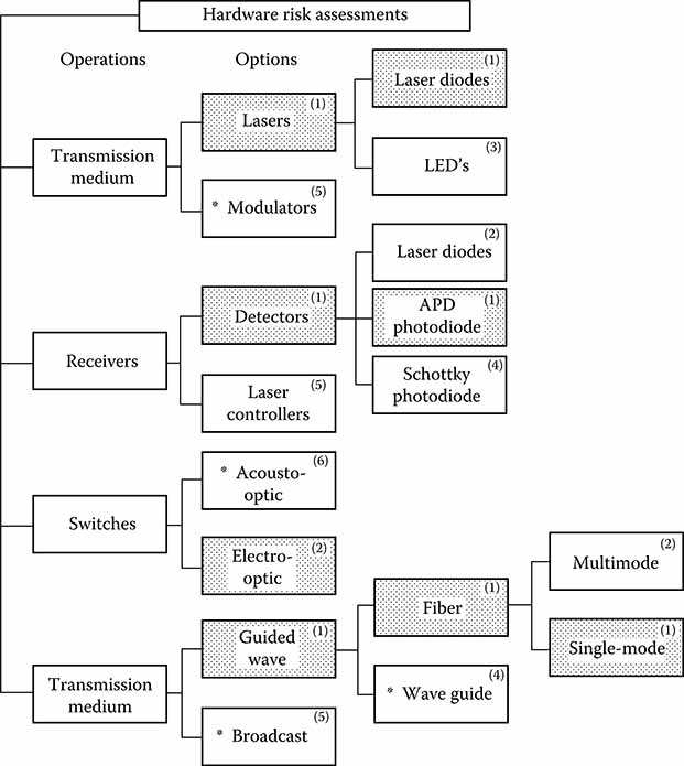
FIGURE 2.32
Hardware risk assessments.
The development of key technologies has made LSI insertion into systems feasible using individual commercial components for optical data interconnects. Input and output terminals are dimensionally comparable to present day bonding pads. Power dissipation for optical elements can be made from a small fraction of total chip power dissipation and all high-speed data input and output can be performed by optical means. The conclusion is that optical interconnects are possible and sensible for intraboard and cabinet-level applications. There is no single optical interconnect approach suitable for every application, but rather each application will require separate consideration for the design of optical data links.
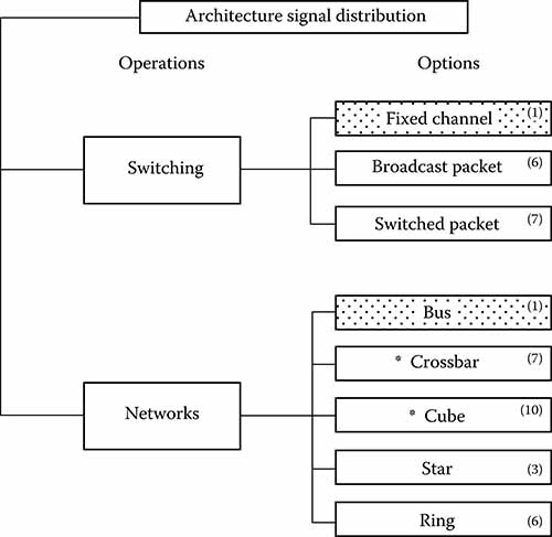
FIGURE 2.33
Architecture risks.
2.11 Electro-Optic System Applications
2.11.1 Special Application Lighting and Laser Illumination
An interesting test application for lasers is producing sufficient illumination to acquire high-speed video (frame rates up to a million frames per second) and to image through high-luminosity events such as fireballs. Previous laser illumination systems [84–87] required complex pulse timing, extensive cooling, large-scale laser systems (frequency-doubled flash-pumped Nd:YAG, Cu-vapor, Q-switched ruby), making them difficult to implement for illumination in high-speed videography. Requirements to illuminate through the self-luminosity of explosive events motivated the development of high-brightness imaging techniques obviating the limitations of previous attempts. Vertical cavity surface-emitting laser (VCSEL) arrays and a lens system were utilized with temporal and spectral filtering to effectively remove self-luminosity and fireball from the image, providing excellent background discrimination in a variety of range test scenarios.
Use of laser illumination in conjunction with narrow bandpass filtering and electro-optic shuttered temporal filtering provides background discrimination for high-resolution, high-speed digital image processing. In addition, the characteristics of the VCSEL structures now available represent viable lighting characteristics for other illumination events currently using flash-bulbs and argon discharge lamps. Timing sequences for shuttering, modulation, camera synchronization, exposure time, and digital image frame rate are integrated with a high degree of accuracy, permitting high resolution, blur- and distortion-free, quantitative video realization of high-speed events and associated data processing. Illumination from a VCSEL array is virtually speckle free. Measurements show that the illuminated area has speckle of <1%. Therefore, VCSEL illumination is very desirable for many applications where uniformity of illumination is very important.
Laser illumination can be applied in a broad range of applications. In some it may be necessary to pulse the laser for gated imaging. This technique can be used for 3-D imaging and also for improving the signal-to-noise ratio at a desired depth. In gated imaging, a synchronized triggering signal is sent to both the camera and the laser. Short pulses are then emitted from the laser and the reflected light from the scene is accepted at desired time delays. Other applications do not require gating.
Areas of interest may include
Shaped charge detonations to further understand the properties of jet formation and particulation
Explosively formed projectile detonations to quantify launch and flight performance characteristics
Detonations of small caliber grenades and explosive projectiles to verify fuse function times and fragmentation patterns
Performance and behavior of various projectiles and explosive threats against passive, reactive, and active target systems
Human effects studies including body armor, helmets, and footwear
Behind armor debris studies of large caliber ammunition against various armor materials
Small caliber projectile firings to study launch, free flight, and target impact results
Professional sporting events
Two key technologies are routinely utilized to achieve adequate scene illumination for high-speed video capture: flashbulbs and discharge tubes. Output curves for the frequently used PF-200 and PF-300 flashbulbs are shown in Figure 2.34. The peak output of 6.0 × 10⁶ lm translates to 477,465 cd. Bulbs are flashed, for instance, at 28 ms prior to the key portion of a video stream, so that for a 5- to 10-ms window, the target scene is illuminated at or above 90% of the peak flash output. The timing of the peak flash output and the character of the flash event were confirmed with .cine files obtained with a Vision Research Phantom V7.3 high-speed digital imaging system.
FIGURE 2.34
Flashbulb characteristics.
An example of the next-brightest light source, arc discharge tubes, currently identified and used for high-speed imaging, is the Luminys Corporation 6.5-K Blast high-intensity light. This source produces 25,863 cd, but for a significantly longer duration, depending on the charging characteristics. A typical illumination event for the 6.5-K Luminys light is shown in Figure 2.35.
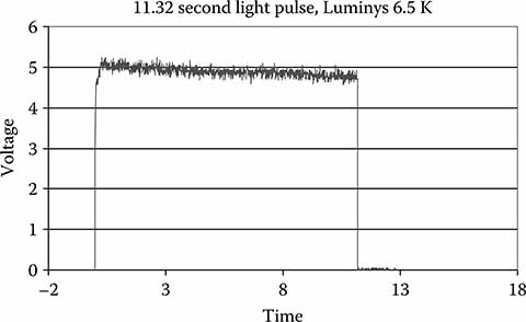
FIGURE 2.35
Time history of Luminys Corporation’s 6.5-K light system.
2.11.2 Vertical Cavity Surface Emitting Lasers for Illumination
VCSELs were historically limited to low-power applications; but through several Defense Advanced Research Projects Agency (DARPA) sponsored programs [88], the output power of VCSELs dramatically improved. Princeton Optronics (PO) Corporation developed the world’s highest power single devices and 2-D arrays [89]. They have successfully demonstrated single devices with >3 W continuous wave (CW) output power and large 2-D arrays with >230 W CW output power. These arrays comprise thousands of small, low-power, single-mode devices. The output of this array can then be focused into a very small, low-diverging spot using a microlens array focusing-lens system. VCSELs have several major advantages in illumination applications [89]:
A circular output beam.
Much lower wavelength dependence to temperature (5× less than for edge emitters). Since the VCSEL resonant cavity is defined by a wavelength-thick cavity sandwiched between two distributed Bragg reflectors (DBRs), devices emit in a single longitudinal mode and the emission wavelength is inherently stable (<0.07 nm/K), without the need for additional wavelength stabilization schemes or external optics, as is the case for edge emitters.
A much higher reliability than edge emitters since VCSELs are not subject to catastrophic optical damage (COD) failures.
High-temperature operation. VCSELs and VCSEL arrays can be operated at temperatures up to 80°C ambient without chillers.
High power from the arrays (demonstrated CW power density of 1200 W/cm2 from the arrays).
Emission wavelength is very uniform across a 5 mm × 5 mm VCSEL array, resulting in spectral widths of ~0.7 to 0.8-nm full width at half maximum (FWHM).
VCSELs can be easily processed into large 2-D arrays (do not need stacking) to scale up the power. The 2-D array configuration provides for more efficient heat-sinking and better pump power density, as the devices can be very closely packed.
Low thermal resistance for CW operation. A thermal resistance of 0.15°C/W from the junction temperature to the microcooler coolant makes it lower by more than a factor of 2 compared with edge-emitter arrays.
VCSEL arrays are designed for coupling match to COTS microlens arrays.
PO makes single-mode devices at wavelengths of 976 and 1064 nm, as well as custom wavelengths between 808 and 1064 nm.
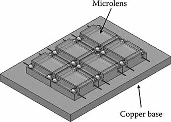
FIGURE 2.36
Six-VCSEL array configuration (current configurations contain nine).
As a starting point, we consider the optical output needed to achieve a luminous intensity comparable to that of the arc discharge lamp (25,000 lm). A single-VCSEL array will deliver 70 W at 976 nm. With 1 W = 680 lm at 550 nm, and a correction factor of 7 (assuming a camera QE of 35% at 550 nm and 5% at 976 nm), the equivalent single-VCSEL output at 976 nm is about 6800 lm. A 9-VCSEL device will deliver about 61,200 lm of focused light onto its target. It can be expected that the VCSEL will improve lighting by more than one f-stop, and the source can be used at extended distances.
The arrays are connected serially and mounted on a copper base (Figure 2.36). For 150-ms operation, the heat released is about 95 J. The specific heat of copper is 0.385 J/g°K; therefore, for 100 g of copper submount, the temperature increase is only 2.5°C, which allows passive cooling.
Nebolsine et al. [85] developed estimates for shaped charge jets and radiometric characterization with video cameras. The approach was to determine illumination levels for a laser illuminator needed to overcome the jet luminosity and provide sufficient exposure for imaging. This general concept was used to evaluate candidate laser technologies for suitability in system design. The VCSEL approach provides flexibility, in that it can be utilized in a range of timing and illumination test scenarios. The pulse length can be essentially CW, with minimal cooling requirements; while the illumination brightness can be increased through the addition of more arrays in the package configuration.
2.11.3 Spectral Matching Considerations
The monochrome spectral response curve for the Vision Research Phantom V7.3 high-speed video camera used in the author’s laboratory is shown as the dark curve in Figure 2.37. While light sources such as the Luminys 6.5-K lamp exhibit broadband spectral content (Figure 2.38), similar to the flashbulbs, VCSEL sources produce a 976-nm center wavelength, with a FWHM spectral width of 0.8 nm. For this reason, the response of the V7.3 at 976 nm is an important parameter for our system design. As mentioned previously, the ratio of the quantum efficiency at 550 nm to the efficiency at 976 nm is about 7.
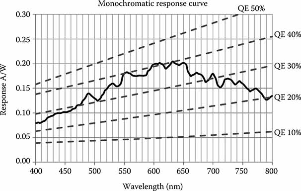
FIGURE 2.37
Spectral sensitivity of Phantom v7.3 high-speed digital imaging system.
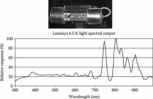
FIGURE 2.38
Normalized spectral output of Luminys Corp. 6.5-K light.
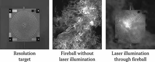
FIGURE 2.39
Laboratory demonstration of single-VCSEL illuminator.
2.11.4 High-Brightness Imaging
The system developed is intended for a wide variety of illumination scenarios. The VCSEL can be pulsed and operated uncooled for the duration of short events (e.g., 150–200 ms), as was the case with previous work in laser illuminators, where the light source determined the temporal sample size for the event. For longer event applications, it can be operated CW and in a cooled configuration. In CW operation, the temporal characteristics of high-speed capture are determined by the camera.
For imaging applications involving the liner collapse, jet formation, and progression of a detonated shaped charge, some camera timing capabilities may not be fast enough to fully characterize the event. Typical jet velocities approach 10–12 km/s [85, 92]. In these cases, one might consider, for instance, the Imacon 200 ultra high-speed camera, with frame rates up to 200 million frames per second, or 5-ns samples.
Use of VCSELs for laser illumination applications shows great promise as a versatile, readily implemented approach to a host of current challenges for high-speed imaging. A technology demonstration phase utilizing a single-VCSEL array has been performed in the author’s laboratory. A view from the demonstration is shown in Figure 2.39. This illustrates the ability to see through a fireball using laser illumination and narrow bandpass filtering. The utility of the VCSEL illumination is readily apparent. A fielded brass board 9-VCSEL model, shown below in Figure 2.40, is now in testing in live fire applications.
2.12 Vertical Cavity Surface Emitting Laser Technology
Princeton Optronics (PO), in Trenton, New Jersey, is the leader in commercial VCSEL technology. The following information (Section 2.12) is courtesy of PO and Dr. Chuni Ghosh.
FIGURE 2.40
Nine-VCSEL laser illuminator.
2.12.1 Introduction
VCSELs are a relatively recent type of semiconductor laser. These were first invented in the mid-1980s. Very soon, they gained the reputation as a superior technology for short reach applications such as fiber channel, Ethernet, and intrasystems links. Within the first 2 years of commercial availability (1996), VCSELs became the technology of choice for short range datacom and local area networks, effectively displacing edge-emitter lasers. Mentzer, Naghski, and a team of IBM researchers developed the first VCSEL-based parallel 12-channel fiber-optic data link [93]. This success was mainly due to the VCSEL’s lower manufacturing costs and higher reliability compared to edge emitters.
PO developed the key technologies resulting in the world’s highest power single-VCSEL devices and 2-D arrays, demonstrating single devices with >5 W CW output power and large 2-D arrays with >230 W CW output power. They made single-mode devices of 1 W output power and single-mode arrays with power of >100 W, which are coupled to 100u, 0.22NA fiber. The highest wall plug efficiency of these devices and arrays is 56%. Arrays delivered 1 kW/cm2 in CW operation and 4.2 kW/cm2 in QCW operation. PO participated in the DARPA-SHEDS program, whose main objective was to improve laser diode power conversion efficiency.
2.12.2 VCSEL Structure
Semiconductor lasers consist of layers of semiconductor material grown on top of each other on a substrate (the “epi”). For VCSELs and edge emitters, this growth is typically done in an MBE or MOCVD growth reactor. The grown wafer is then processed accordingly to produce individual devices. Figure 2.41 summarizes the differences between VCSEL and edge-emitter processing.
In a VCSEL, the active layer is sandwiched between two highly reflective mirrors (dubbed DBRs) made up of several quarter-wavelength-thick layers of semiconductors of alternating high and low refractive index. The reflectivity of these mirrors is typically in the range of 99.5%–99.9%. As a result, the light oscillates perpendicular to the layers and escapes through the top (or bottom) of the device. Current and/or optical confinement is typically achieved through either selective-oxidation of an aluminum-rich layer, ion-implantation, or even both for certain applications. The VCSELs can be designed for “top-emission” (at the epi–air interface) or “bottom-emission” (through the transparent substrate), in cases where “junction-down” soldering is required for more efficient heat sinking, for example. Figure 2.42 illustrates different common types of VCSEL structures.
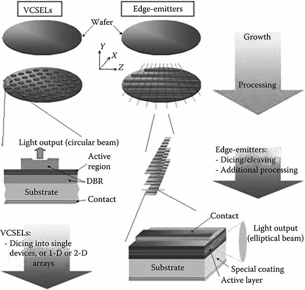
FIGURE 2.41
Comparison of the growth/processing flow of VCSEL and edge-emitter semiconductor lasers. (Courtesy of Princeton Optronics [PO] and Dr. Chuni Ghosh. With permission.)
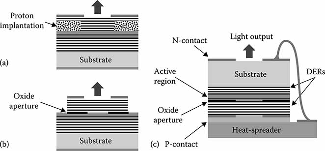
FIGURE 2.42
Three common types of VCSEL structures: (a) a top-emitting structure with proton implantation to confine the current, (b) a selectively oxidized top-emitting structure to confine the optical modes and/or the current, and (c) a mounted bottom-emitting selectively oxidized structure. (Courtesy of Princeton Optronics [PO] and Dr. Chuni Ghosh. With permission.)
In contrast, edge emitters are made up of cleaved bars diced from the wafers. Because of the high index of refraction contrast between air and the semiconductor material, the two cleaved facets act as mirrors. Hence, in the case of an edge emitter, the light oscillates parallel to the layers and escapes sideways. This simple structural difference between the VCSEL and the edge emitter has important implications.
Since VCSELs are grown, processed, and tested while still in the wafer form, there is significant economy of scale resulting from the ability to conduct parallel device processing, whereby equipment utilization and yields are maximized, and setup times and labor content are minimized. In the case of a VCSEL (see Figure 2.41), the mirrors and active region are sequentially stacked along the Y-axis during epitaxial growth. The VCSEL wafer then goes through etching and metallization steps to form the electrical contacts. At this point, the wafer goes to test where individual laser devices are characterized on a pass-fail basis. Finally, the wafer is diced and the lasers are binned for either higher level assembly (typically >95%) or scrap (typically <5%). Figure 2.43a shows a single high-power VCSEL device (>2 W output power) packaged on a high-thermal conductivity submount. Figure 2.43b shows the L–I characteristics of a 5 W VCSEL device.
In a simple Fabry–Pérot edge emitter, the growth process also occurs along the Y-axis, but only to create the active region, as mirror coatings are later applied along the Z-axis. After epitaxial growth, the wafer goes through the metallization step and is subsequently cleaved along the X-axis, forming a series of wafer strips. The wafer strips are then stacked and mounted into a coating fixture. The Z-axis edges of the wafer strips are then coated to form the device mirrors. This coating is a critical processing step for edge emitters, as any coating imperfection will result in early and catastrophic failure of the devices due to COD. After this coating step, the wafer strips are diced to form discrete laser chips, which are then mounted onto carriers. Finally, the laser devices go into test.
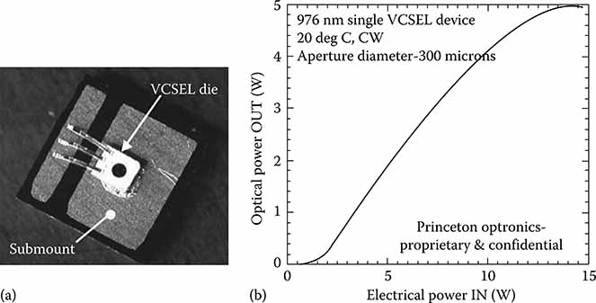
FIGURE 2.43
(a) 3 Packaged high-power VCSEL device (>2 W). The submount is 2 mm × 2 mm. (b) Shows the L-I characteristics of a 5 W VCSEL device. The device aperture is 300 u. (Courtesy of Princeton Optronics [PO] and Dr. Chuni Ghosh. With permission.)
It is also important to understand that VCSELs consume less material: in the case of a 3″ wafer, a laser manufacturer can build about 15,000 VCSEL devices or approximately 4,000 edge emitters of similar power levels. In addition to these advantages, VCSELs demonstrate excellent dynamic performance such as low threshold current (a few microamperes), low-noise operation, and high-speed digital modulation (10 Gb/s). Furthermore, although VCSELs have been typically utilized in low-power applications—a few milliwatts at most—they have the inherent potential of producing very high powers by processing large 2-D arrays, as discussed in the section describing high-brightness illumination. In contrast, edge emitters cannot be processed in 2-D arrays.
2.12.3 VCSEL Advantages
The many additional advantages offered by the VCSEL technology can be summarized in the following points:
Wavelength stability: The lasing wavelength in a VCSEL is very stable, since it is fixed by the short (1- to 1.5-wavelength-thick) Fabry–Pérot cavity. Contrary to edge emitters, VCSELs can only operate in a single longitudinal mode.
Wavelength uniformity and spectral width: Growth technology has improved such that VCSEL 3″ wafers are produced with <2 nm standard deviation for the cavity wavelength. This allows the fabrication of VCSEL 2-D arrays with little wavelength variation between the elements of the array (<1 nm FWHM spectral width). By contrast, edge-emitter bar-stacks suffer from significant wavelength variations from bar to bar since there is no intrinsic mechanism to stabilize the wavelength, resulting in a wide spectral width (3–5 nm FWHM).
Temperature sensitivity of wavelength: The emission wavelength in VCSELs is approximately five times less sensitive to temperature variations than in edge emitters. The reason is that in VCSELs, the lasing wavelength is defined by the optical thickness of the single-longitudinal mode cavity and that the temperature dependence of this optical thickness is minimal (the refractive index and physical thickness of the cavity have a weak dependence on temperature). On the other hand, the lasing wavelength in edge emitters is defined by the peak-gain wavelength, which has a much stronger dependence on temperature. As a consequence, the spectral line-width for high-power arrays (where heating and temperature gradients can be significant) is much narrower in VCSEL arrays than in edge-emitter arrays (bar-stacks). Also, over a 20°C change in temperature, the emission wavelength in a VCSEL will vary by <1.4 nm (compared to ~7 nm for edge emitters).
High-temperature operation (Chillerless operation for pumps): VCSEL devices can be operated without refrigeration because they can be operated at temperatures to 80°C, the cooling system becomes very small, rugged, and portable with this approach.
Higher power per unit area: Edge emitters deliver a maximum of about 500 W/cm2 because of gaps between bar to bar that must be maintained for coolant flow, while VCSELs are delivering ~1200 W/ cm2 now and will deliver 2–4 kW/cm2 in the near future.
Beam quality: VCSELs emit a circular beam. Through proper cavity design, VCSELs can also emit in a single transverse mode (circular Gaussian). This simple beam structure greatly reduces the complexity and cost of coupling/beam-shaping optics (compared to edge emitters) and increases the coupling efficiency to the fiber or pumped medium. This has been a key selling point for the VCSEL technology in low-power markets.
Reliability: Because VCSELs are not subject to COD, their reliability is much higher than for edge emitters. Typical FIT values (failures in one billion device-hours) for VCSELs are <10.
Manufacturability and yield: Manufacturability of VCSELs has been a key selling point for this technology. Because of complex manufacturing processes and reliability issues related to COD, edge emitters have a low yield (edge-emitter 980-nm pump chip manufacturers typically only get ~500 chips out of a 2″ wafer). On the other hand, yields for VCSELs exceed 90% (corresponds to ~5000 high-power chips from a 2″ wafer). In fact, because of its planar attributes, VCSEL manufacturing is identical to standard IC Silicon processing.
Scalability: For high-power applications, a key advantage of VCSELs is that they can be directly processed into monolithic 2-D arrays, whereas this is not possible for edge emitters (only 1-D monolithic arrays are possible). In addition, a complex and thermally inefficient mounting scheme is required to mount edge-emitter bars in stacks.
Packaging and heat-sinking: Mounting of large high-power VCSEL 2-D arrays in a “junction-down” configuration is straightforward (similar to microprocessor packaging), making the heat-removal process very efficient, as the heat must traverse only a few microns of AlGaAs material. Record thermal impedances of <0.16 K/W have been demonstrated for 5 mm × 5 mm 2-D VCSEL arrays.
Cost: With the simple processing and heat-sinking technology, it becomes much easier to package 2-D VCSEL arrays than an equivalent edge-emitter bar-stack. The established silicon industry heat-sinking technology can be used for heat removal for very high-power arrays. This will significantly reduce the cost of the high-power module. Currently, cost of the laser bars is the dominant cost for the DPSS lasers.
High-wavelength stability and low-temperature dependence: Since the VCSEL resonant cavity is defined by a wavelength-thick cavity sandwiched between two DBRs, devices emit in a single longitudinal mode and the emission wavelength is inherently stable (<0.07 nm/K), without the need for additional wavelength stabilization schemes or external optics, as is the case for edge emitters. Furthermore, thanks to advances in growth and packaging technologies, the emission wavelength is very uniform across a 5 mm × 5 mm VCSEL array, resulting in spectral widths of 0.7–0.8 nm (FWHM). (see Figures 2.44 and 2.45.)
Wavelength stability and narrow spectral width are very significant advantages in pumping applications, for example, where the medium has a narrow absorption band.
Unlike edge emitters, VCSELs emit in a circularly symmetric beam with low divergence without the need for additional optics. This has been a tremendous advantage for low-power VCSELs in the telecom and datacom markets because of their ability to directly couple to fibers (“butt-coupling”) with high coupling efficiency. PO high-power VCSEL arrays emit in a quasi-top-hat beam profile, making these devices ideal for direct pumping (“butt-pumping”) of solid-state lasers.
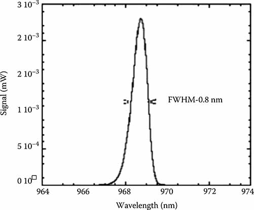
FIGURE 2.44
Emission spectrum of a 5 mm × 5 mm VCSEL array at 100 W output power (120 A). (Courtesy of Princeton Optronics [PO] and Dr. Chuni Ghosh. With permission.)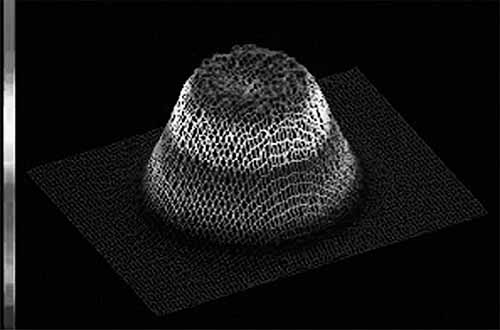
FIGURE 2.45
Far-field beam profile of a 5 mm × 5 mm VCSEL array at 100 W output power (120 A). (Courtesy of Princeton Optronics [PO] and Dr. Chuni Ghosh. With permission.)Feedback insensitivity: In VCSELs, the as-grown output coupler reflectivity is very high (typically >99.5%) compared to edge emitters (typically <5%). This makes VCSELs extremely insensitive to optical feedback effects, thus eliminating the need for expensive isolators or filters in some applications.
Low thermal impedance and ease of packaging: PO developed advanced packaging technologies, enabling efficient and reliable die-attach of large 2-D VCSEL arrays on high-thermal-conductivity submounts. The resulting submodule layout allows for straightforward packaging on a heat exchanger.
For high-power devices packaged on microcoolers, PO demonstrated modules with thermal impedances as low as 0.15 K/W (between the chiller and the chip active layer).
2.12.4 High-Power CW and QCW VCSEL Arrays
PO designs and manufactures advanced high-power CW and QCW diode lasers for the industrial, medical, and defense markets. Unlike edge emitters, the light emits perpendicular to wafer surface for VCSELs. It is therefore a straightforward to process 2-D arrays of small VCSEL devices driven in parallel to obtain higher output powers. The advantage of 2-D arrays is the simple silicon IC chip-like configuration. Many of the silicon IC packaging and cooling technologies can be applied to VCSEL arrays.
PO took the VCSEL technology to very high power levels by developing very large (5 mm × 5 mm) 2-D VCSEL arrays packaged on high-thermal-conductivity submounts. (see Figure 2.46). These arrays are composed of thousands of low-power single devices driven in parallel. Using this approach, record CW output powers in excess of 230 W from a 0.22 cm2 emission area (>1 kW/cm2) have been demonstrated, without sacrificing wall-plug efficiency.
In addition to CW VCSEL arrays, PO has developed very high power density VCSEL arrays for quasi-CW (QCW) operation. QCW powers in excess of 925 W have been demonstrated from very small arrays (5 × 5 mm chip size), resulting in record power densities >4.2 kW/cm2 (see Figure 2.47). These small arrays can easily be connected in series to form larger arrays with high output powers. These arrays are ideal for applications requiring very compact high-power laser sources.
Because VCSELs can operate reliably at temperatures up to 80°C, they do not necessarily require refrigeration. Additionally, since the wavelength change with temperature is small, the cooling system design can be considerably simplified. The cooling system thus becomes very small, rugged, and portable with this approach. We have been operating the VCSELs and VCSEL arrays with water pump and a radiator cooling like that of a car engine. Figure 2.48 shows such a setup in which a radiator and water pump is used to cool a 120 W array of VCSELs. The result of the cooling arrangement is compared with a chiller cooling and shown in Figure 2.43.
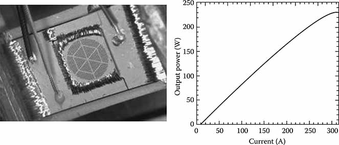
FIGURE 2.46
Picture of high-power 5 mm × 5 mm 2-D VCSEL array mounted on a micro-cooler and measure CW output power and voltage at a constant heat-sink temperature. Roll-over power is >230 W. (Courtesy of Princeton Optronics [PO] and Dr. Chuni Ghosh. With permission.)
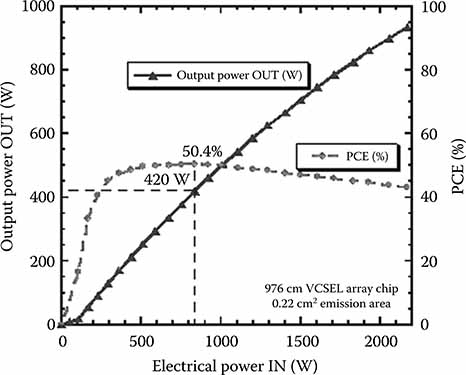
FIGURE 2.47
Power versus current for a small VCSEL 2-D array under different QCW regimes. These arrays exhibit power densities of >4.2 kW/cm2. (Courtesy of Princeton Optronics [PO] and Dr. Chuni Ghosh. With permission.)
Figure 2.49a shows the performance of a 120 W VCSEL array with fanradiator cooling with water temperature at 45°C versus cooling with a chiller with 16°C water temperature. The green curves show the efficiency (CE) in the two cases, which is almost similar. The red curves show the power output from the array in the two cases. The power output decreases somewhat at higher power, but at power levels below 80 W, there is very little change. Figure 2.49b shows the L–I curves for a QCW array at 808 nm at different temperatures. The top curve is at 20°C and the bottom one is at 85°C.
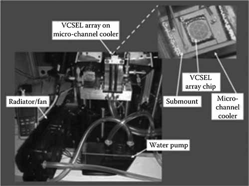
FIGURE 2.48
Shows the setup without chiller using a radiator and a water pump in an arrangement like in a car engine.
2.12.5 VCSEL Reliability
In terms of reliability, VCSELs have an inherent advantage over edge emitters because they are not subject to COD. Indeed, the problem of sensitivity to surface conditions for edge emitters is not present in VCSELs because the gain region is embedded in the epistructure and does not interact with the emission surface.
Over the years, several reliability studies for VCSELs have yielded FIT rates (number of failures in one billion device-hours) on the order of 1 or 2, whereas FIT rates for the highest telecom-grade edge emitters is on the order of 500. The failure rate for industry-grade high-power edge-emitter bars or stacks is even worse (>1000).
PO has accumulated millions of device-hours on VCSELs operating above 100°C. This reliability advantage will be very significant for laser systems, where the end-of-life and field failures are overwhelmingly dominated by pump failure. Moreover, VCSEL arrays can be operated at higher temperatures, resulting in lower power consumption of the overall laser system.
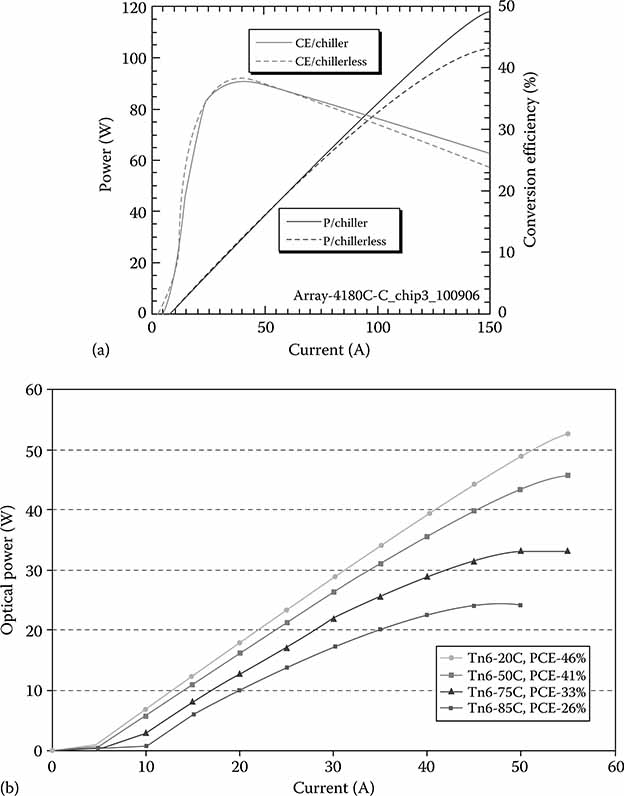
FIGURE 2.49
(a) Performance of a 120 W VCSEL array with fan-radiator cooling. (b) L–I curves for a QCW array at 808 nm at different temperatures. (Courtesy of Princeton Optronics [PO] and Dr. Chuni Ghosh. With permission.)
2.12.6 Single-Mode VCSEL Devices
PO makes single-mode devices with power levels of 5 mW for small-aperture devices (4 μm) as well as higher power devices of power output of 150 mW from 100 μm aperture devices in TO can packages and up to 1 W from a single device in a larger package. The devices have narrow linewidths of tens of kilohertz and SMSR of >30 dB. The devices have high efficiency of >40%.
2.12.7 High-Speed VCSEL Devices
High-speed VCSEL devices are in development. Current devices work to 5 GHz speed. Figure 2.50 shows the performance of a 4 μm aperture device performing at >5 GHz speed. A power level of >5 mW is achieved at these speeds.
2.12.8 High-Brightness Arrays of Single-Mode Devices
VCSELs are also a new technology for pumping of solid state lasers, including fiber lasers. Because of their circular beam and excellent optical characteristics, it is possible to make high-brightness pumps using an array of closely spaced single-mode VCSEL devices. The arrays are temperature stable and operate at high temperatures without chillers. They are lower cost as they do not require expensive operations like cleaving of the wafers. These fiber coupled arrays can be combined for higher output power using fiber combiners and coupled with double core fiber to develop small, high-performance fiber lasers working at elevated temperatures without chillers.
For high-brightness devices and arrays, PO makes self-lasing VCSELs or extended or external cavity VCSELs and couples such arrays into fibers using microlenses as shown in Figure 2.51.
2.12.9 Blue, Green, and UV VCSELs
PO developed very high quality blue lasers from VCSELs by frequency doubling the VCSEL radiation with a nonlinear material. The blue laser output at 480 nm is single-mode and highly monochromatic with a beam divergence (half angle) of 8 mR. The VCSEL devices and arrays are capable of delivering very high power in a 2-D array and hence frequency doubled arrays are able to deliver very high levels of power. PO developed 6 W of peak power from a single-VCSEL device that was frequency doubled and is working toward a 10 mJ pulse, 1 kHz rep rate blue laser in a small form factor. Figure 2.52 shows the schematic of the approach and Figure 2.53 shows the experimental setup for the blue laser using VCSELs.
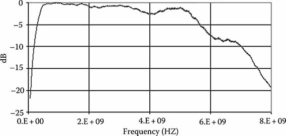
FIGURE 2.50
A 4 u aperture single-mode device shows high-speed performance through >5 GHz. The device power is >5 mW.
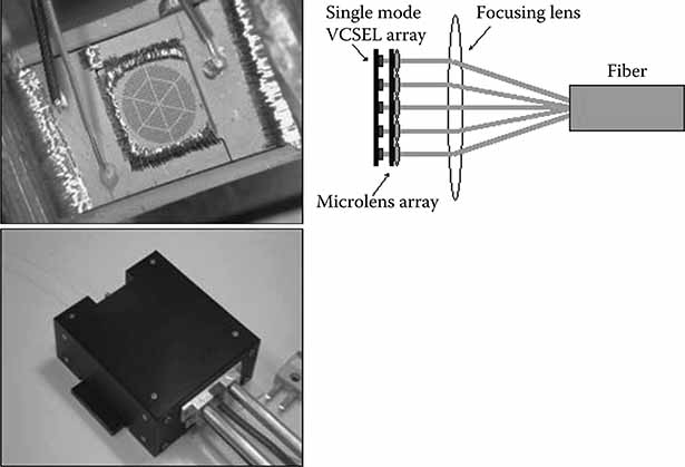
FIGURE 2.51
This figure shows a 100 W CW single-mode VCSEL array mounted on a microcooler (top left). On top right, it shows the single-mode array coupling scheme to couple the array with the fiber. At bottom left, it shows the package that has a dimension of (2 × 1.5 × 0.5″), which is water cooled. (Courtesy of Princeton Optronics [PO] and Dr. Chuni Ghosh. With permission.)
For UV lasers, an external frequency doubler material BGO doubles the frequency of the laser. PO is developing several millijoules of UV energy per pulse from these devices with kilohertz repetition rate. Figure 2.54 shows the schematics of the approach obtaining 1 mJ pulse energy, with a 100 Hz repetition rate.
2.12.10 Narrow Divergence Arrays
VCSEL arrays with microlens collimation become very narrow divergence light sources. A single-mode array (Figure 2.55) shows the collimation of the beams from individual VCSELs. Using a microlens aligned with the VCSEL array and held in position by laser-welding the holding frames produces divergence of 60 mrad (full angle) for self-lasing arrays and 8 mrad (full angle) for external cavity arrays. Figure 2.56 shows schematically the collimation architecture using microlenses. Using external lenses as shown in Figure 2.56, one can achieve very narrow divergence with VCSEL arrays. A divergence of 0.5 mrad has been achieved using an expander lens and a focusing lens.
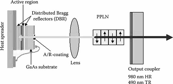
FIGURE 2.52
This figure shows the schematic of blue laser generation. An external cavity approach is used in which the PPLN is put inside the cavity. We have developed green laser using this approach as well. A peak power of 6 W from a single VCSEL has been obtained with this approach. (Courtesy of Princeton Optronics [PO] and Dr. Chuni Ghosh. With permission.)
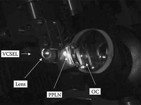
FIGURE 2.53
This figure shows the experimental setup for frequency doubling of VCSEL devices. PPLN material is used for frequency doubling. PO is working on frequency doubling of high-power arrays. A peak power of 6 W from a single device has been obtained. (Courtesy of Princeton Optronics [PO] and Dr. Chuni Ghosh. With permission.)
As discussed previously, VCSELs provide excellent illumination sources for high-luminosity lighting requirements, such as high-speed videography. PO developed an area illuminator module at 808 nm that can be used to illuminate a large area. The module has a power output 400 W and can be used to illuminate an area of 1.5 km × 1.5 km. Figures 2.57 and 2.58 show the diagram of the module as well as the picture of it.

FIGURE 2.54
This figure shows the schematics of the frequency-doubling approach to UV wavelengths. We are working toward developing lasers with several millijoules per pulse with 1 kHz repetition rate. (Courtesy of Princeton Optronics [PO] and Dr. Chuni Ghosh. With permission.)
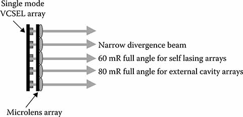
FIGURE 2.55
This figure shows the architecture of collimating the individual beams from the VCSELs in the array by means of a microlens array. (Courtesy of Princeton Optronics [PO] and Dr. Chuni Ghosh. With permission.)
Similar VCSEL illuminators are used with silicon CCD or CMOS cameras for illumination for perimeter security, area illumination, border security etc. Figures 2.59 and 2.60 show diagrams for these illuminators that are small form factor, have high efficiency, and have low cost.
2.12.11 VCSEL-Based 1064 nm Low-Noise Laser
PO developed a novel approach for low-noise lasers with extremely low noise using VCSELs. For high-power operation, efficient heat removal is required and therefore a junction-down, bottom-emitting structure is preferred to improve current injection uniformity in the active region and to reduce the thermal impedance between the active region and the heat spreader. A schematic of the structure without the heat spreader is shown in Figure 2.61.
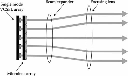
FIGURE 2.56
This figure shows the architecture of collimating the individual beams from the VCSELs and further reducing their divergence by using a beam expander and a focusing lens. A divergence of 0.5 mR can be achieved from the entire array with this approach. (Courtesy of Princeton Optronics [PO] and Dr. Chuni Ghosh. With permission.)
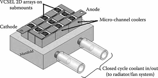
FIGURE 2.57
The diagram of the 400 W illuminator module. The dimensions of the module is 2.5 × 1.5 × 5.5″. (Courtesy of Princeton Optronics [PO] and Dr. Chuni Ghosh. With permission.)
For current and optical confinement, the selective oxidation process is used to create an aperture near the active region to improve performance. A low-doped GaAs N-type substrate is used to minimize absorption of the output light while providing electrical conductivity for the substrate-side N-contact. The growth is performed in a MOCVD or MBE reactor and starts with an AlGaAs N-type partially reflecting DBR. The active region consists of InGaAs quantum wells designed for 1064 nm emission and strained-compensated using GaAsP barriers. The active region is followed by a high-reflecting P-type DBR. A high-aluminum content layer is placed near the first pair of the P-DBR to later form the oxide aperture. The placement and design of the aperture are critical to minimize optical losses and current spreading. Band-gap engineering (including modulation doping) is used to design low-resistivity DBRs with low-absorption losses.
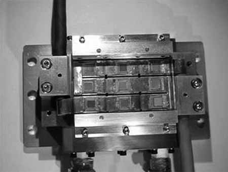
FIGURE 2.58
Picture of the module. (Courtesy of Princeton Optronics [PO] and Dr. Chuni Ghosh. With permission.)
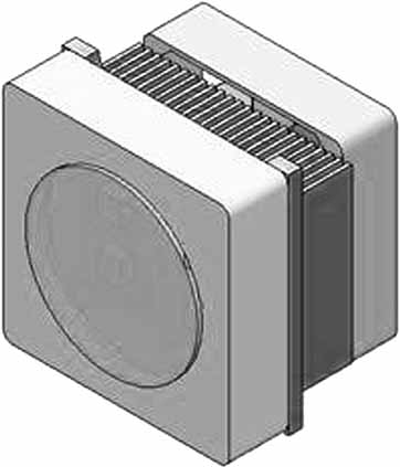
FIGURE 2.59
Diagram of a 3 and 8 W illuminator (808 nm). The dimensions of the illuminator is 2 × 2 × 2″ and uses 15 W input power for 3 W output and 40 W for 8 W output. The beam divergence is 16°. (Courtesy of Princeton Optronics [PO] and Dr. Chuni Ghosh. With permission.)
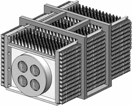
FIGURE 2.60
Diagram of a 40 W output illuminator. The input power for the illuminator is 200 W. The dimension of the illuminator is 7.5 × 6.5 × 12 in. (Courtesy of Princeton Optronics [PO] and Dr. Chuni Ghosh. With permission.)
FIGURE 2.61
Schematic of the selectively oxidized, bottom-emitting 1064 nm VCSEL structure. (Courtesy of Princeton Optronics [PO] and Dr. Chuni Ghosh. With permission.)
2.12.12 Low-Noise Laser Cavity
The low-noise laser cavity is shown in Figure 2.62. The optical setup consists of a VCSEL device and an output coupler. A high-quality Etalon and a Brewster plate in the cavity control the single-wavelength operation and linear polarization, respectively. The optical isolator prevents optical feedback from outside of the cavity to maintain the single-wavelength operation. The beam is then coupled into a PM fiber with a focusing lens for the mode matching.
FIGURE 2.62
The low-noise laser cavity with an etalon and a Brewster plate can be seen. (Courtesy of Princeton Optronics [PO] and Dr. Chuni Ghosh. With permission.)
2.13 Derivation of the Linear Electro-Optic (Pockels) Effect
The linear electro-optic effect is the result of distortion of the crystal lattice caused by an applied electric field. The effect is manifested as an induced birefringence in the crystal that results in field dependent changes in the refractive index along various crystal axes, thus affecting the phase of the transmitted electric field. The electro-optic effect can be derived using the Index Ellipsoid (IE) notation. A complete derivation for 43 m crystals can be found in Namba and an example can be found in Yariv [94]. The procedure is to transform the standard IE to a coordinate system rotated to match the symmetry of the field of interest.
As an example, Figure 2.63 shows an exaggerated diagram of a Double-Y Mach Zehnder optical logic gate [95] (see also Chapter 3) on a GaAs wafer, indicating the relative orientation of the device and the crystal. The crystal axes are indicated using standard notation. It should be noted that due to the relationship between wafer orientation and the crystal axis of rotation, it is only practical to apply an external field along a single crystal axis.
The standard IE is written
IE=1n20(x2+y2+z2)+2r41(Exyz+Eyxz+Exxy)(2.7)
For this discussion, we assume the applied dc field is in the x direction only, along the <100> axis; therefore,
FIGURE 2.63
Wafer orientation of double-Y device.
E=Ex′andIE=1n20(x2+y2+z2)+2r41(Eχyz)(2.8)
We transform the standard IE to primed coordinates. By symmetry
x′=x′′x=x′x2=x′2(2.9)
By inspection
y′=y√2+Z√2;y′=y√2+Z′√2,z′=(-y)√2+Z√2,z′=y′√2+Z′√2y2=y′22+Z′22+y′z′z2=y′22+Z′22+y′z′yz=y′22-Z′22(2.10)
Substituting into IE,
IE=x′2(1n20)+y′2(1n20+r41Ex)+z′2(1n20-r41Ex)(2.11)
The standard primed IE’ is
IE'=χ′2n2x+y′2n2y+Z′2n2z(2.12)
Equating IE = IE′ and assuming 1≫n20r41Ex
n′s=n0n′s=n0(1−r41n202Ex)y′=y√2+z√2≫y=y′√2−z′√2n′x=n0(1+r412n20Ex)z′=−y√2+z√2=z=y′√2+z√2y2=y′22+z′22−y′z′z2=y′22+z′22+y′z′yz=y′22−z′22(2.13)
This index change is
Δn=ni′-ni′=n0(2.14)
or
Δnx=0Δny′=-r41n302ExΔnx′=+r41n302Ex
The results of this analysis show that one must consider both the waveguide alignment and the polarization of the optical field launched in the waveguide. This shows that an index change is encountered only by field components lying in the plane of the wafer. Furthermore, the index change depends on the crystal direction of the optical propagation.
The index change will vary from positive along the directions <011> or <0¯11> to negative along the directions <01ˉ1> and <0ˉ11>; along four of the crystal axes, <001>, <00ˉ1>, <010>, and <0ˉ10>, the positive and negative changes cancel and there is no net index change.
To determine the ideal waveguide direction, two points must be considered. First, arbitrary polarization of the launched E-field will generally result in an induced elliptical polarization. Only by launching the field parallel to the wafer will the linear polarization be maintained. The second consideration is that the waveguiding of any optical field is accomplished by making the guiding region a higher index of refraction than the cladding; therefore, it is usually desirable to align the guide such that the index change is positive and leads to greater confinement.
With these points in mind, we use the waveguide alignment shown in Figure 2.64. The optical TE mode is launched in the <011> direction and the E-field is parallel to the <0ˉ11> or Z′ axis. The important effect for the operation of the double-Y device example is that the induced index change can be related to a phase change in the launched optical field; therefore, the field splitting to the guide with the applied dc field will undergo a phase advance relative to the field that travels through the neutral guide.
The phase change for a given length l of the guide is
Δ∅=2πλΔnl(2.15)
The applied field in the x direction can be rewritten in terms of the applied voltage Ex = V/t, where V is the applied voltage and t is the guide thickness. Then
Δn′=r41n30V2t(2.16)
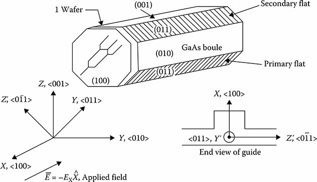
FIGURE 2.64
Crystal orientation of waveguides for the determination of electro-optic coefficients.
Substituting Equation 2.16 into Equation 2.15 yields
Δ∅=πλr41n30Vlt(2.17)
As an example, we calculate the value of applied voltage necessary to induce a phase change of π radians for a length of waveguide l. The material parameters for a GaAs waveguide are n0 = 3.46, r41 = 1.2 × 10⁻¹² m/V. Assuming an operating wavelength of 850 nm and a guide thickness of t = 1 μm, we find that V = 0.018/l V or, given a 1 cm electrode interaction length, V = 1.8 V.
2.14 Nonlinear Refractive Index
The nonlinear refractive index is a third-order optical effect as opposed to the Pockels effect, which is a second-order effect. The discussion that follows is intended to explain the fundamental theoretical basis of all nonlinearities. A wide variety of third-order nonlinear optical effects is found to be related through the complete formalism of nonlinear optical susceptibilities. Among these are ellipse rotation, the “dc” Kerr effect, the optical (or “ac”) Kerr effect, self-focusing, self-phase modulation, phase conjugation, and four-wave mixing.
The problem to be addressed is to solve Maxwell’s equations when there are current and charge densities brought about by the interaction of light with matter (or in a vacuum where the light interacts with itself). The physical origin of these interactions is the nonlinear polarizability of either the electronic charge cloud around the nuclei or a change in the various types of nuclear motion allowed by the degrees of freedom of the material. These are referred to as either the electronic or nuclear contributions. Although the charge densities can be explained as a series of monopoles, this is found not to be applicable in the optical regime, and instead a generalized electric polarization is used. A further approximation used is the electric-dipole approximation that essentially states that the polarization is local. This in turn makes the problem independent of spatial coordinates. With this in mind, Maxwell’s equations take the form
∇XE=-1∂Ec∂t∇XB=1c∂∂t(E+4πP)+4πcIdc∇⋅(E+4πP)=0∇⋅B=0(2.18)
P is the local polarization and is the only time-varying source term. It is in general a function of E and fully describes the response of the medium to the field. At this point, the assumption is generally made that the electric field is sufficiently weak such that the total optical polarization density can be expanded as a power series in the electric field:
→P=χ(1)⋅→E+χ(2):→E→E+χ(3):χ(3)→E→E→E+...(2.18a)
where χ(n) is the nth order complex optical susceptibility. This can be shown to be valid when the optical field is less than the atomic field, that is, when E < Eat ≈ 1 × 10⁹ V/cm. A full quantum mechanical derivation dealing with the microscopic interactions in the material is necessary to exactly calculate the susceptibilities [96, 97].
The exact form of the effect observed is dependent on the frequencies of the optical fields and the polarization of their E-fields relative to the crystal axes. The frequency dependency occurs because of interactions with various resonances in the crystal. These can range from slow thermal effects (response ~1 s) to fast vibrations (response ~10−15 s). Drastic differences can occur as the excitation frequency moves across a resonance. This is clearly exhibited by excitonic effects in semiconductor quantum well structures.
For third-order effects, we are particularly interested in the term χ(3). The real and imaginary parts of this term give rise to nonlinear refraction and absorption, respectively. The third-order contribution to the total polarization in Equation 2.18 can be written as
P3i(ω4)=Σj,k,lχ3ijkl(ω4;ω1,ω2,ω3)Ej(ω1)Ek(ω2)(El)(ω3)(2.19)
In general, the tensor χ3ijkl can have 81 individual elements. Fortunately, many of the elements are found to be zero or equal to each other due to various crystal symmetries. In particular, with GaAs being a ˉ43 class crystal, the tensor reduces to 21 nonzero elements of which only 4 are independent. The frequencies of the four fields in Equation 2.19 may be of any form satisfying the conservation of energy:
ω4=ω1+ω2+ω3(2.20)
The fields of interest in the Double-Y Mach Zehnder Logic Gate, for example, are a strong pump beam of frequency ωp, and a weaker probe beam of frequency ωpr. It is found that the problem is simplified as long as the probe beam is not strong enough to affect the pump beam. Although it is not necessary for this theoretical development to make a restriction on the relationship between these frequencies, generally the beams will come from the same source material so we set ωp = ωpr. Equation 2.19 can then be written as
P3i(ωpr)=Σi,j,k,lχ3ijkl(−ωpr;ωpr,ωp,ωp)Ej(ωpr)Ek(ωp)(Ei)(ωp)(2.21)
The effect of interest in the Double-Y example is the alteration of the refractive index Δn by the pump beam intensity in the waveguide that in turn alters the path length for the weaker probe beam. The subsequent index can be written in the form
n=n0+γ〈E2〉(2.22)
or
n=n0+n2I
where n0 is the linear refractive index. It should be noted that Equation 2.22 is often written in other forms. In addition, either electrostatic units (esu) or SI units (mks) are frequently used. For this reason, we now list various conversion factors that can be used between the nonlinear coefficients [98].
γ[esu]=(en040π)n2[m2/W]γ[cm3/erg]=n0(238.7)n2[cm2/W]γ[m2/V2]=n0(3.333×10-6)n2[cm2/W]γ[cm3/erg]=(7.162×107)γ[m2/V2](2.23)
The change in path length is usually written as a phase difference relative to a wave propagating in the other leg of the interferometer. In terms of the nonlinear index, this change can be written in the form [99]
Δ∅=ωprcn2l(2.24)
where l is the interaction length of the pump and probe beams. It is the relationship of the nonlinear index n2, or the index change Δn, to the third-order susceptibility that is finally developed, usually written as
n2=Δn(E2)(2.25)
The last three factors to consider are the crystallographic orientation along which the pump and probe beams travel, the polarization of these beams, and the optical frequency that is used. Because it is quite lengthy to discuss the relationships for general crystallographic directions and polarizations, we give only the results for the <011> orientation and crossed beam polarizations used in the Double-Y device. As for the frequencies of the beams, two cases may be developed that are termed the resonant and nonresonant cases.
The nonresonant case is the simpler of the two and is based on the Born–Oppenheimer (BO) approximation. The assumption is made that the electrons follow the optical fields and nuclear motions adiabatically; that is, the optical frequency is much too low to interact with the electronic vibrations. On the other hand, the frequency is still too fast to interact with the far-infrared vibrational frequencies. It is further assumed that the frequency is far from any absorption resonances. This approximation further increases the symmetry of the problem so as to reduce the number of independent elements of the susceptibility tensor to three. Generally, this is the situation when using wavelengths of lower energy than the bandgap in the Double-Y semiconductor waveguides. It is then found that the nonlinear index may be expressed [100].
Δn=12πn0χ(3)1122(esu)(2.26)
The second case is with the pump frequency close to the semiconductor band edge frequency of the waveguide. This is the situation when using GaAs sources with AlGaAs waveguides. In this case, a different derivation was developed by Jensen and Torabi [101] taking into account photon absorption and electron–hole recombination processes. It is found that the index variation goes from the first power dependence on the intensity, described by Equation 2.22, to a dependence of the form
n=n0+n3I1/3
In this case, the nonlinear index is written as
n3I1/3=Δn=8c03z2n0Nγ(ατ0ℏω)1/3(2.27)
where we use the n3 to differentiate cases and where c0, Nγ, α, and τ0 are various physical constants of the material. The parameter z is a normalized frequency.
Finally, as an example, we calculate the optical power necessary for a phase change of π radians according to Equation 2.24 (assuming a 1 cm interaction length). A typical value of the nonlinear index for GaAs is n2 ≈ 2 × 10⁻¹³ cm2/W that indicates a required intensity of approximately 250 MW/cm2 [102]. For a typical waveguide cross section of 4 μm2, this indicates a required coupled input power of 10 W. Although this is an extremely high power for use in an integrated optical circuit, recent work with MQW structures suggests that the large nonlinearity observed in these materials will enhance the refractive index nonlinearity. This would conceivably allow the use of a reduced intensity while still achieving the necessary phase change. Experiment suggests intensities as low as 104 W/cm2 may be effective, which corresponds to milliwatt power levels in the waveguides.
References
1. Midwinter, J. E. 1985. Current status of optical technology. J. Lightwave Technol. LT-3:927.
2. Craley, D. E., L. R. Megargel, M. A. Mentzer, and D. H. Naghski. 1987. Interconnects for VHSIC packaging. Proc. SPIE 85:328–336 (August).
3. Bhasin, K. B., G. Anzic, R. R. Kunath, and D. J. Connolly. 1986. Optical techniques to feed and control GaAs MMIC modules for phased array antenna applications. Paper presented at the 11th Annual Communications Conference, March 16–20, in San Diego, CA.
4. Bhasin, K. P., G.E. Ponchak, and T. J. Kascak. 1985. Monolithic optical integrated control circuitry for GaAs MMIC-based phased arrays. Proc. SPIE 578 (September). (Presentation only.)
5. Mentzer, M. A. and D. E. Craley. 1987. Optical interconnects. Paper presented at the IGK Conference on Fiber Optic Communications and Local Area Networks (FOC/ LAN’87), October, in Anaheim, C.A.
Hutcheson, L. D. and M. A. Mentzer. 1986. Design criteria for AlGaAs integrated optoelectronic devices. Proc. SPIE 704 (September).
Hutcheson, L. D. 1985. Optical interconnect technology. Paper presented at the Annual OSA Meeting, October 19–24, in Seattle, WA.
6. Hutcheson, L. D., P. R. Haugen, and A. Husain. 1985. Gigabit per second optical chip-to-chip interconnects. Proceedings of the SPIE, November, in Cannes, France.
7. Pucel, R. 1985. Monolithic Microwave Integrated Circuits. New York: IEEE Service Center.
8. Liao, S. Y. 1980. Microwave Devices and Circuits. Englewood Cliffs, NJ: Prentice-Hall, Inc.
9. Stutzman, W. L. and G. A. Thiele. 1981. Antenna Theory and Design. New York: John Wiley & Sons.
10. Chilton, R. H. 1987. MMIC T/R modules and applications. Microw. J. 30:131, 132, 134, September.
11. Johnson, R. C. and H. Jasik. 1984. Antenna Applications Reference Guide. New York: McGraw-Hill Book Co.
12. Brookner, E. 1987. Array radars: an update part 1. Microw. J. 30:117–138, February.
13. Tang, R. and R. Brown. 1987. Cost reduction techniques for phased arrays. Microw. J. 30:139–146, January.
14. Liao, S. Y. 1980. Microwave devices and circuits. New Jersey: Prentice-Hall, Inc.
15. Ibid.
16. Streetman, B. G. 1980. Solid State Electronic Devices. Englewood Cliffs, NJ: Prentice-Hall, Inc.
17. Wang, K. and S. Wang. 1987. State-of-the-art ion-implanted low-noise GaAs MESFET’s and high-performance monolithic amplifiers. IEEE Trans. Electron Devices ED-34(12):2610–2615 (December).
18. Liao. Microwave devices and circuits.
19. Hunsperger, R. G. and M. A. Mentzer. 1988. Optical control of microwave devices: a review. Proceedings of the SPIE Integrated Optical Circuit Engineering VI, September, in Boston, MA.
20. Herczfeld, P. R., A. S. Daryoush, A. Rosen, P. Stabile, and V. M. Contarino. 1985. Optically controlled microwave devices and circuits. RCA Rev. 46:528–551(December).
21. Seeds, A. J., J. F. Singleton, S. P. Brunt, and J. R. Forrest. 1987. The optical control of IMPATT oscillators. IEEE J. Lightwave Technol. LT-5 (3):403–410 (March).
Seeds, A. J. and J. R. Forrest. 1981. Reduction of FM in IMPATT oscillators by optical illumination. Electron. Lett. 17(23):865–866 (November 12).
Kiehl, R. A. 1980. Optically induced AM and FM in IMPATT diode oscillators. IEEE Trans. Electron. Devices ED-27(2):426–432 (February).
Seeds, A. J. and J. R. Forrest. 1978. Initial observations of optical Injection locking of an X-band IMPATT oscillator. Electron. Lett. 14(25):829–830 (December 7).
Yen, H. W. 1980. Optical injection locking of Si IMPATT oscillators. Appl. Phys. Lett. 38(8):630–631 (April 15).
Forrest, J. R. and A. J. Seeds. 1978. Optical injection locking of IMPATT oscillators. Electron. Lett. 14(19):626–627 (September 14).
Herczfeld, P. R., A. S. Daryoush, A. Rosen, A. K. Sharma, and V. M. Contarino. 1986. Indirect subharmonic optical injection locking of a millimeter-wave IMPATT oscillator. IEEE Trans. Microw. Theory Tech. MTT-34(12): 1371–1476 (December).
Daryoush, A. S., P. R. Herczfeld, Z. Turski, and P. K. Wahl. 1986. Comparison of indirect optical injections-locking techniques of multiple X-band oscillators. IEEE Trans. Microw. Theory Techn. MTT-34(12):1363–1367 (December).
Yen, H. W., M. K. Barnoski, R. G. Hunsperger, and R. T. Melville. 1977. Switching of GaAs IMPATT diode oscillator by optical illumination. Appl. Phys. Lett. 31(2):120–122 (July 15).
Vyas, H. P., R. J. Gutmann, and J. M. Borrego. 1979. The effect of hole versus electron photocurrent on microwave-optical interactions in IMPATT oscillators. IEEE Trans. Electron Devices ED-26(3):232–234 (March).
Schweighart, A., H. P. Vyas, J. M. Borrego, and R. J. Gutmann. 1978. Avalanche diode structures for microwave-optical interactions. Solid State Electron. 21:1119–1121.
22. Kiehl, R. A. 1978. Behavior and dynamics of optically controlled TRAPATT oscillators. IEEE Trans. Electron. Devices ED-26(6):703–710 (June).
Gleichauf, P. H. and E. P. Eernisse. 1977. Control of TRAPATT oscillations by optically generated carriers. IEEE Trans. Electron. Devices 24(3):275–277 (March).
23. Salles, A. A. and J. R. Forrest. 1981. Initial observations of optical injection locking of GaAs metal semiconductor field effect transistor oscillators. Appl. Phys. Lett. 38:392–394(March 1).
24. Yen, H. W. and M. K. Barnoski. 1978. Optical injection locking and switching of transistor oscillators. Appl. Phys. Lett. 32:182–184(February 1).
25. Sze, S. M. 1981. Physics of Semiconductor Devices. New York: John Wiley & Sons, Inc.
26. Hunsperger and Mentzer. Optical control of microwave devices. A Review Proc. SPIE. 993:204–224(1988).
27. Seeds, A. J., J. F. Singleton, S. P. Brunt, and J. R. Forrest. 1987. The optical control of IMPATT oscillators. J. Lightwave Technol. 5(3):403–411.
28. Seeds, A. J. and J. R. Forrest. 1981. Reduction of FM noise in IMPATT oscillators. Electron. Lett. 17(23):865–866.
29. Kiehl, R. A. 1980. Optically induced AM and FM. IEEE Trans. Electron Devices 27(2):426–432.
30. Seeds, A. J. and J. R. Forrest. 1978. Initial observations of optical injection locking. Electron. Lett. 14(25):29–830.
Yen, H. W. 1980. Optical injection locking of Si IMPATT oscillators. Appl. Phys. Lett. 36:680–683.
Forrest, J. R. and Seeds, A. J. 1978. Optical injection locking of IMPATT oscillators. Electron. Lett. 14:626–627.
Herczfeld, P. R. et al. Indirect subharmonic optical injection locking. 1986. IEEE Trans. Microw. Theory Techn. MTT-34:1371–1376 (December).
Daryoush, A. S. et al. 1986. Comparison of indirect optical injection-locking techniques. IEEE Microw. Theory Techn. 34(12):1363–1370.
31Forrest, J. R. and A. J. Seeds. 1978. Optical injection locking of IMPATT oscillators. Electron. Lett. 14:626–627.
32. Sze. Physics of Semiconductor Devices.
33. Kiehl, R. A. 1978. Behavior and dynamics of optically controlled TRAPATT oscillators. IEEE. Electron Devices ED-25:703–710.
Gleichauf, P. H. and E. P. Eernisse. 1977. Control of TRAPATT oscillations. IEEE Trans. Electron Devices 24(2):275–277.
34. Salles, A. A. and J. R. Forrest. 1981. Initial observations of optical injection locking. Appl. Phys. Lett. 38(5):392–394.
35. Yen and Barnoski. Optical injection locking and switching of transistor oscillators. Appl. Phys. Lett.
36. Contarino, V. M. and A. Ortiz. A high speed phase shifter based on optical injection. RCA Review 46:528–551(December 1985).
37. Stallard, W. A., A. R. Beaumont, and R. C. Booth. 1986. Integrated optic devices for coherent transmission. J. Lightwave Technol. LT-4(7):852–857 (July).
Alferness, R. C. 1986. Titanium diffused lithium niobate waveguide devices. ISAF’86 Proceedings, June 8–11 in Bethlehem, PA.
Russ, D. 1986. The use of lithium niobate devices in optical networks. Proceedings SPIE 630 Fiber Optics’86, in London (SIRA).
Valdmanis, J. A. 1986. High speed optical electronics: The picosecond optical oscilloscope. Solid State Technology: Test and Measurement World S40–S44(November).
Korotky, S. et al. 1986. Integrated optical narrow line width laser. Appl. Phys. Lett. 49(1):10–12 (July 7).
Korotky, S. 1987. Optical intensity modulation to 40 GHz using a waveguide electro-optic switch. Appl. Phys. Lett. 50(23):1631–1633 (June 8).
38. Fontaine, M., A. Delage, and D. Landheer. 1986. Modeling of Ti diffusion into LiNbO3 using a depth dependent diffusion coefficient. J. Appl. Phys. 60(7):2343 (October).
Valdmanis, J. A. High speed optical electronics. Solid State Technol.
39. Russ, D. The use of lithium niobate devices. SPIE.
40. Ibid.
41. Young, T. P., K. K. Wong, A. C. O’Donnell, and N. J. Parsons. 1987. A compact LiNbO3 optical switch at 1.3 μm. GEC J. Res. 5(1):62–64.
Alferness, R. C. 1986. Titanium diffused lithium niobate waveguide devices. ISAF’86 Proceedings, June 8–11, in Bethlehem, PA.
42. Russ. The use of lithium niobate devices. SPIE.
43. Alferness, R. C. Titanium diffused lithium niobate. ISAF.
44. Russ. The use of lithium niobate devices. SPIE.
45. Parsons, N. J., A. C. O’Donnell, and K. K. Wong. 1986. Design of efficient and wideband traveling-wave modulators. Proceedings I.O.C.E. III, April 16–18, in Innsbruck, Austria.
Holman, R., L. Altman-Johnson, and D. Skinner. 1986. The desirability of electro-optic ferroelectric materials for guided wave devices. Proceedings IEEE’86, CH2358-0/86/000-0032.
Gee, C. M. et al. 1983. 17 GHz bandwidth electro-optic modulator. Appl. Phys. Lett. 43(11):998–1000 (December).
Eknoyan, O. et al. 1986. Guided-wave electro-optic modulators in Ti:-LiNbO3 at 2.6 μm. J. Appl. Phys. 59(8):2993–2995 (April 15).
46. Schmidt, R. V. and R. C. Alferness. 1979. Photonic switches and switch arrays on L:N60. IEEE Trans. Circuits Syst. CAS-26:1099.
47. Alferness, R. C. and L. L. Buhl. 1981. Waveguide electro-optic polarization transformer. Appl. Phys. Lett. 38:655–657.
Donaldson, A. and K. K. Wong. 1987. Phase-matched mode convertor in LiNbO3 using near-Z-axis propagation. Electron. Lett. 23(25):1378–1379 (December 3).
Alferness. R. C. Titanium diffused lithium niobate. ISAF.
48. Russ. The use of lithium niobate devices. SPIE.
49. Chung, P. S. 1986. Integrated electro-optic modulators and switches. J. Electrical Electron. Eng. 6(4) (December) (Australia IE Aust. and IREE Aust).
50. Wong, K. K. and R. M. DeLaRue. 1983. An improved electro-optic waveguide serrodyne frequency translator in X-cut LiNbO3 using proton-exchange. Paper presented at the 1st International Conference on Optical Fiber Sensors, April 26–28, in London, England.
51. Stallard, W. A., A. R. Beaumont, and R. C. Booth. 1986. Integrated optic devices for coherent transmission. J. Lightwave Technol. LT-4(7):852–857 (July).
52. Alferness. Titanium diffused lithium niobate. ISAF.
53. Zang, D. and C. Tsai. 1985. Single mode waveguide microlenses and microlens arrays fabricated in LiNbO3 using titanium indiffused proton exchanged technique. Appl. Phys. Lett. 46:703–705.
54. Mentzer and Craley. Optical interconnects. Proceedings I6K. FOC/LAN’87.
55. Craley, D. E., L. R. Megargel, M. A. Mentzer, and D. H. Naghski. 1987. Interconnects for VHSIC packaging. Proceedings of the SPIE 835 Integrated Optical Circuit Engineering V, August, in San Diego, CA.
56. LSI Logic Data Book: Bipolar and CMOS LSI/VLSI. Dallas, TX: Texas Instruments, Inc.: 3–37.
57. VHSIC Device Specifications Reference Book, VHSIC Program Office (1987).
58. Ibid.
59. Grothe, H., G. Muller, and W. Harts. 1983. 560 mb/s transmission experiments using 1.3 μm InGaAsP/InP LED. Electron. Lett. 19(22):909–911.
60. Bowers, J. E., B. R. Hemenwaw, T. J. Bridges, and E. G. Burkhardt. 1986. Design and implementation of high-speed InGaAsP constricted mesa laser. Paper presented at the IEE Conference on Optical Fiber Communication, February 24, in Atlanta, GA.
61. Husain, A. 1984. Optical interconnect of digital integrated circuit and systems. Proc. SPIE 466:18.
62. Law, H. D., K. Hakano, and L. P. Tomasetta. 1979. State-of-the-art performance of GaAlAs/GaAs avalanche photodiodes. Appl. Phys. Lett. 53:180.
63. Hutcheson and Mentzer. Design criteria for AlGaAs/GaAs. Lecture Cambridge, 1983.
64. Hutcheson, Haugen, and Husain. 1987. Optical interconnects replace hardware. J. IEEE Spectrum. 24(3):30–35.
Hartman, D.H., M. K. Grace, and F. V. Richard. 1986. An effective lateral fiber-optic electronic coupling and packaging technique suitable for VHSIC applications. J. Lightwave Technol. LT-4:73.
65. Hutcheson, L. D. 1986. GaAs/AlGaAs Monolithic optoelectronics and integrated optics. Technical Digest of Conference on Lasers and Electro-Optics, June 9–13, in San Francisco, CA.
66. Hutcheson and Mentzer. Design criteria for AlGaAs/GaAs. SPIE.
67. Ury, I., S. Margalit, M. M. Yust, and A. Yariv. 1979. Monolithic integration of an injection laser and a metal semiconductor field effect transistor. Appl. Phys. Lett. 34:430.
Fukuzawa, T., N. Nakamura, M. Hiras, T. Kuroda, and J. Umeda. 1979. Monolithic integration of a GaAlAs injection laser with a Schottky gate field effect transistor. Appl. Phys. Lett. 36:181.
Katz, J., N. Bar-Chaim, P. C. Chen et al. 1980. A monolithic integration of GaAs/ AlGaAs bipolar transistor and heterostructure laser. Appl. Phys. Lett. 37:211.
Ury, K. Lau, N. Bar-Chaim, and A. Yariv. 1982. Very high frequency GaAlAs laser field-effect transistor monolithic integrated circuit. Appl. Phys. Lett. 41:126.
Kim, M., C. Hong, D. Kasemset, and R. Milano. 1983. GaAlAs/GaAs integrated optoelectronic transmitter using selective MOCVD epitaxy and planar ion implantation. Proceedings of the IEEE GaAs IC Symposium, October, in Monterey, CA.
68. Carney, J., M. Helix, R. Kolbas, S. Jamison, and S. Ray. 1983. Integrated optoelectronic transmitter. Proc. SPIE 408, April.
Kolbas, R., J. Carney, J. Abrokwak, E. Kalweit, and M. Hitchell. 1982. Planar optical sources and detectors for monolithic integration with GaAs Metal semiconductor field-effect transistor (MESFET) electronics. Proc. SPIE 321, January.
Carney, J. K., M. J. Helix, R. M. Kolbas, S. A. Jamison, and S. Ray. 1982. Monolithic optoelectronic/electronic circuits. Proceedings of the IEEE GaAs IC Symposium, October.
Kim, M. E., C. S. Hong, D. Kasemset, and R. A. Milano. 1984. GaAlAs/GaAs integrated optoelectronic transmitter. IEEE EDL.10.1109:306–309.
Kilcoyne, M. K., D. Kasemset, R. Asatourian, and S. Beccue. 1986. Optical data transmission between high speed digital integrated circuit chips. Proc. SPIE 625:127.
69. Carney, H., R. Kolbas, S. Jamison, and S. Ray. 1983. Integrated optoelectronic transmitter. Proc. SPIE. 408.
70. Blauvelt, H. N. Bar-Chaim, D. Fekete, S. Margalit, and A. Yariv. 1982. AlGaAs lasers with micro-cleaved mirrors suitable for monolithic integration. Appl. Phys. Lett. 40:2891.
71. Carney, J., M. Helix, and R. M. Kolbas. 1983. Gigabit optoelectronic transmitter. Proceedings of the IEEE GaAs IC Symposium, October.
72. Walton, M. P., P. R. Haugen, and S. L. Palmquist. 1986. A 1 Gbit/s optical/ electrical input monolithic GaAs transmitter IC. Proceedings of the IEEE MTT-S International Microwave Symposium, June, in Baltimore, MD.
73. Ray, S. and M. P. Walton. 1986. Monolithic optoelectronic receiver for Gbit operation. Proceedings of the IEEE MTT-S International Microwave Symposium, June, in Baltimore, MD.
74. Kilcoyne, Kasemset, Asatourian, and Beccue. Optical data transmission. SPIE.
75. Ibid.
76. Midwinters, J. E. and J. R. Sten. 1978. Propagation studies of graded index fiber installed on cable in operation duct route. IEEE Trans. Commun. COM-26 (7):1015–1020 (July).
77. Yariv, A. 1976. Introduction to Optical Electronics, 2nd ed. New York: Holt, Rinehart, and Winston.
78. Ross, W. E., D. Psaltis, and R. H. Anderson. 1982. Two-dimensional magneto-optic spatial light modulator for signal processing. Proc. SPIE 341:192.
79. Goodman, J. W., A. R. Dias, and L. M. Woody. 1978. Fully parallel, high-speed incoherent optical method for performing the discrete Fourier transform. Opt. Lett. 2(1):1–3.
80. Dapkus, P. D. 1982. Optical communication for IC’s. Rockwell International Report, DTIC no. AD-A112239, March.
81. 1981. WDM advances enhance fiber-optic links. EDN News, February 20:1.
82. Schmidt, R. V. and I. P. Kaminow. 1975. Acousto-optic Bragg deflection in LiNbO3 Ti-diffused waveguides. IEEE J. Quantum Electron. QE-11 (1) January: 57–59.83
83. Alferness, R. C. 1982. Waveguide electro-optic modulators. IEEE Trans. Microwave Theory Tech. MIT-30 (8):1121–1137 (August).
84. Francis, C. L. and Instrument Development Team. 1994. Enhanced imagery through laser illumination (white paper). U.S. Army Aberdeen Test Center, Aberdeen Proving Ground, MD.
85. Nebolsine, Peter, Christopher Rollins, and Edmond Lo. 1994. High-frame rate data collection for advanced armor instrumentation enhanced imagery. Final report, subcontract no. FMD9401. Physical Sciences Inc., October.
86. Nebolsine, P., D. R. Snyder, and J. M. Grace. 2001. MHz class repetitively Q-switched, high-power ruby lasers for high-speed photographic applications. Paper presented at AIAA Aerospace Sciences Meeting, January, in Reno, NV.
87. Piehler, T., B. Homan, R. Ehlers, R. Lottero, and K. McNesby. 2006. High speed laser imaging, emission and temperature measurements of explosions. (ARL-RP-137). Proceedings of the Insensitive Munitions & Energetic Materials Technology Symposium, April, in Bristol, UK.
88. Defense Advanced Research Projects Agency Microsystems Technology Office. Super high efficiency diode sources (SHEDS) program. www.darpa.mil/mto/programs/sheds/index.html.
89. Seurin, J.F., C. L. Ghosh, V. Khalfin, et al. 2008. High-power high-efficiency 2-D VCSEL arrays. Proc. SPIE 6908:690808.
90. Shaw, L. L., L. L. Steinmetz, W. C. Behrendt et al. 1984. A high-speed, eight-frame electro-optic camera with multipulsed ruby laser illuminator. Lawrence Livermore National Laboratory, UCRL-90478, September.
91. Shaw, L. L., S. A. Muelder, A. T. Rivers, J. L. Dilnaure, and R. D. Breithanpt. 1992. Electro-optic frame photography with pulsed ruby illumination. Lawrence Livermore National Laboratory, UCRL-JC-112232, November.
92. Baum, D. W., L. L. Shaw, S. C. Simonson, and K. A. Winer. 1993. Linear collapse and early jet formation in a shaped charge. Proceedings of the14th International Symposium on Ballistics 2, September 26–29:13–22.
93. Freitag, L., J. Kaczynkski, M. Mentzer, and D. Naghski. 2000. Packaging aspects of the LITEBUS™ parallel optoelectronic module. Proceedings of the ECTC, May, in Las Vegas.
94. Namba, S. 1961. Electro-optical effect of zincblende. J. Opt. Soc. Am. 51(1):76. Yariv, A. 1976. Introduction to Optical Electronics. New York: Holt, Rinehart, and Winston.
95. Mentzer, M. A. 1982. Integrated optical logic devices. Paper presented at the U.S. Army ARDEC Sponsored EMP/Radiation Hardening Workshop, October, in Dover, NJ.
Mentzer, M. A., S. T. Peng, and D. H. Naghski. 1987. Optical logic gate design considerations. Proc. SPIE 835 Integrated Optical Circuit Engineering V., Mark A. Mentzer, ed., August 17–20: 362–377, in San Diego, CA.
Mentzer, M. A. 1988. Optical computing. Paper presented at the Investigator’s Meeting on Semiconductors, Optoelectronic and Magnetic Optic Materials held at the Watertown Arsenal Materials Technology Laboratory, January, in Watertown, MA.
96. Shen, Y. R. 1984. The Principles of Non-Linear Optics. New York: Wiley-Interscience.
97. Hellworth, R. W. 1977. Prog. Quant. Elect 5(1). Pergamon Press.
98. Weber, M. J., ed. 1986. “Optical materials”: Part 1. In Handbook of Laser Science and Technology, vol. III. Boca Raton, FL: CRC Press.
99. Hopf, F. A. and G. I. Stegeman. 1986. Applied Classical Electrodynamics 2: NonLinear Optics. New York: Wiley-Interscience.
100. Hellworth. Prog. Quant. Elect.
101. Jensen, B. and A. Torabi. 1984. Infrared optical materials and fibers III. Proc. SPIE 484:159.
102. Wa, P. L. K., J. E. Sitch, N. J. Mason, J. S. Roberts, and P. N. Robson. 1985. Switching in the far-field of a nonlinear directional coupler. Electron. Lett. 21:26.