
6
Optical Diagnostics and Imaging
6.1 Optical Characterization
A variety of specialized test and characterization techniques are employed in the evaluation of optical circuits. Correlation of the information obtained from each characterization provides a complete analysis of the electronic and optical properties of the optical circuit. These are discussed in the following sections.
Figure 6.1 illustrates the experimental setup most commonly used in end-fire coupled loss measurements. Direct end-fire coupling is achieved by focusing laser light into and out of the waveguide with an appropriate lens system. Systems designed for use with solid-state laser diodes eliminate the elliptical beam pattern and astigmation common in these types of lasers and provide micron spot sizes. Mode selective, nondestructive loss measurements can be performed using the prism coupling technique shown in Figure 6.2. Here, light is evanescently coupled from the prism into a waveguide mode at a specific coupling angle determined by the prism geometry and index and the mode order.
Coupling into multiple closely spaced waveguides on a single chip is also often required. This is most easily accomplished by butt-coupling optical fibers to the input waveguide. A chuck is fabricated from a suitable semiconductor material by etching grooves in the material to hold the fibers. Due to precision of the photolithographic techniques used to etch the grooves and precision of standard optical fiber dimensions, this method provides a highly accurate means of aligning the fibers and waveguides.
The output image can be analyzed by a variety of methods. The method illustrated in Figure 6.2 is to sweep the focused image across a detector-slit combination by use of a scanning mirror. The detector output is displayed on an oscilloscope, with its sweep synchronized to the mirror scan. This approach is often modified to remove the sweeping mirror and detector-slit combination by using a precision stepping motor. The detector output and stepping motor position can drive an X–Y plotter to produce a plot similar to the oscilloscope display of the previous setup.
An alternative to these techniques is the use of a two-dimensional (2-D) self-scanning pyroelectric detector array. This device, when coupled with an oscilloscope and computer, permits storage and output of mode profile and loss information. Figure 6.3 illustrates a typical mode profile obtained using such an instrument.
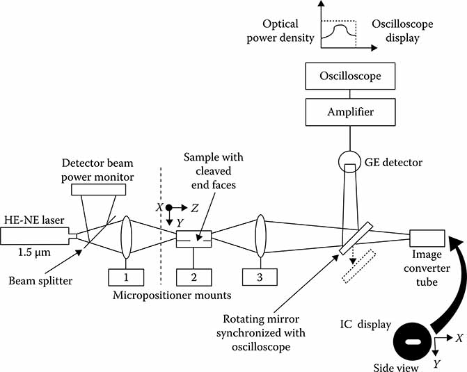
FIGURE 6.1
Mode profile and loss determination setup.
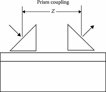
FIGURE 6.2
Prism coupling waveguide loss measurement technique.
Scattering losses can be measured using a fiber-optic probe technique shown in Figure 6.4. For this technique, micropositioners are accurately controlled to guide a fiber probe along the waveguide (while staying far enough away so that coupling is not induced), measuring any radiation scattered out of the waveguide [1]. The use of the fiber probe incorporated in a microscope allows the distance between the fibers and the waveguide surface to be kept constant, thereby improving the accuracy of this technique. The use of relatively high power AlGaAs lasers, which are now commercially available, makes this technique quite viable, as more power input results in more scattered power.
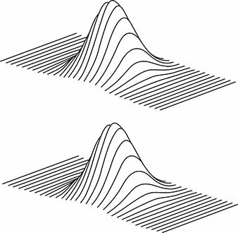
FIGURE 6.3
Representative output from ISC mode profile and loss determination setup.
Several other techniques exist for measuring waveguide propagation loss. A generalization of the fiber probe measurement is to use a video camera to image scattered radiation along the propagation path; then, by employing digital image processing, the propagation loss can be calculated [2]. To use this technique with AlGaAs waveguides, an infrared video camera is often used. Another possibility to measure waveguide propagation loss is the use of Fabry–Perot techniques [3]. Here the optical length of the waveguide or the wavelength of the source is varied over a small range with the output intensity being monitored. The optical length can be changed by slightly heating or cooling the sample, while varying the wavelength of the laser source over a small range by inducing the appropriate variations in the power supply current. Radiation losses are measured in bends in a manner similar to the absorptions loss; however, by calibrating and subtracting the other two loss mechanisms, the loss due to radiation alone can be evaluated.
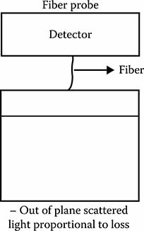
FIGURE 6.4
Fiber probe loss measurement technique.
6.2 Bandwidth Measurement
A key characteristic of optical switches and modulators is their switching speed and modulation depth. For switches, the bandwidth is related to the switching speed by the equation
A modulator’s bandwidth is often expressed as the frequency range over which it can maintain a modulation depth of 50%. Various expressions are used to express the modulation depth, depending on whether the applied electrical signal acts to increase or decrease the intensity of the transmitted light. The respective expressions are given as Equation 6.2:
where
l is the transmitted optical intensity
l0 is the quiescent optical intensity
lm is the optical intensity under maximum electrical signal
To test the active devices for modulation depth and speed, high-speed detectors and storage oscilloscopes are used.
6.3 Stability: Temperature and Time Effects
The most significant problem of the stability of waveguide building blocks and devices is introduced by the temperature dependence of the index of refraction resulting from change in the energy bandgap with temperature. Propagation and attenuation of optical energy in a semiconductor can be described by a complex index of refraction
where the real part of the index is related to the propagation constant β by
and k is related to the absorption coefficient α by
where
v is the light frequency
c is the speed of light in a vacuum
λ0 is the vacuum wavelength of the light
The real and imaginary parts of the complex index of refraction are coupled to each other as described by the Kramer–Kronig relations [4]. This coupling results in a change in the real part of the index n corresponding to any change in the imaginary part k. At wavelengths relatively close to the absorption edge of the semiconductor (i.e., photon energies close to the bandgap energy Eg), the strong dependence of the optical absorption of Eg produces a corresponding dependence of n on Eg. Thus, the dependence of Eg on temperature translates into a dependence of n on temperature. It is possible to obtain an order-of-magnitude estimate of the effect by using some well-known empirical relations. An empirical relation
which is called Moss’s rule has been found to be obeyed by semiconductors whose value of n4 is in the range of 30–440 [5]. Note that for AlxGa(1−x)As, with x = 0 to x = 0.4, n4 is in the range of 164–120. An empirical relation for the bandgap energy of GaAs is given by [6]
for temperatures above 100 K. Using these relations, one would expect an increase in index of refraction of Δn ~ 0.01 (about 0.3%) for an increase in temperature from 273 to 350 K. This is a relatively small change in index compared to the difference in index between the waveguide and confining layers of an AlGaAs waveguide; hence, little change in the light propagation characteristics would be expected. Also, the decrease in bandgap energy from 1.437 to 1.417 eV as the temperature is increased to 350 K should not produce a significant increase in interband absorption, and free-carrier concentration (and hence absorption) would not change significantly. The change in index, however, even though relatively small, could be expected to have a significant effect on interference-based devices such as a Mach–Zehnder interferometer, and operating temperature would have to be taken into account in their design. Individual devices should be tested in situ at various temperatures to determine if temperature variations are a factor affecting the performance of the device.
The long-term effects of time and temperature on waveguide and device operation are difficult to predict theoretically. It is usually necessary to experimentally determine such performance data by conducting life tests on the various devices after they are fabricated.
6.4 Measurement of ND(d) Using Capacitance–Voltage Technique
The capacitance–voltage (C-V) technique is an effective method for determining the dopant profile as well as the width of carrier compensated guiding layers, Schottky barriers, p–n junctions, and heterojunctions. The thickness of the depletion layer is determined from the capacitance of a non-injecting metal contact on the guide surface. The voltage Vp required to form a depletion layer of thickness d in a conducting layer of carrier concentration ND and ∈r is given by
If the bulk breakdown field Ec of the semiconductor is exceeded during the measurement, current flows, the accuracy of the technique is immediately seriously impaired, and the measurement rapidly fails. This occurs when
and limits d to the value
where Ec is approximately 6 × 10⁵ V/cm for ND = 1017. This limits the measurable layer thickness to the values indicated in Figure 6.5. Chemical etching sequences are required to characterize deeper layers. Figure 6.6 shows an automated CV measurement system.
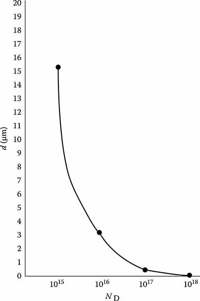
FIGURE 6.5
Thickness of proton implanted waveguide versus carrier concentration, which can be evaluated by a direct CV profile.
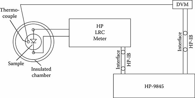
FIGURE 6.6
Block diagram of C-V measurement system.
6.5 “Post Office” Profiling
This system overcomes some of the limitations of the CV technique. The system was originally developed at the British Post Office Research Centre by Gyles Webster [7] to profile carrier concentration in III–V materials. The semiconductor sample is loaded onto a PTFE electrochemical cell where a small area (typically 0.1 or 0.01 cm2) is defined and used to form an electrode. A DC voltage is applied to produce a bias which causes the formation of a Schottky barrier at the material surface; simultaneously, continuous electroetching takes place under illumination. Capacitance and voltage are periodically monitored, in situ, as the etch progresses, in automatic fashion. A continuous profile is obtained, and a plot of log (carrier concentration versus depth) is drawn.
6.6 Spreading Resistance Profiling
The two-point spreading resistance measurement can be used to map the resistivity of a structure as a function of depth. This can provide information concerning the degree of implant damage produced as well as uniformity and abruptness of transition regions. This is in addition to the standard four-point probe measurement of resistivity shown in Figure 6.7.
The spreading resistivity measurement is made with two probes contacting a surface of the material. At least one of the probes is so sharp as to contact the surface with a small circular area of radius r. Applying a voltage across the electrodes causes a flow of current, whose value is restricted by the resistance of the sharp contact. (Often, both contacts are sharp.) This resistance, called the spreading resistance, is caused by the concentration of the current density in the vicinity of the sharp contact and is thus localized at that point of measurement. Its value is given by
where ρ is the resistivity (Ω-cm) in the neighborhood of the probe.
Figure 6.8 shows schematically how the spreading resistance measurement serves to map the carrier concentration in implanted samples. After exposure the samples are cut into test specimens which are cleaned and then lapped to provide an angle of about 5.7° (tangent = 0.1). This angle provides a 10:1 distance magnification in the measurement. The measurements start with both electrodes positioned on the line where the lapped surface meets the original surface at an angle of about 174.3°. After providing a value of the resistance R at that location, the electrodes are advanced to the right in small steps. Steps of 5 μm, for example, correspond to measurements at depth increments of 0.5 μm.
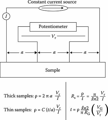
FIGURE 6.7
Four-point probe measurement of resistivity.
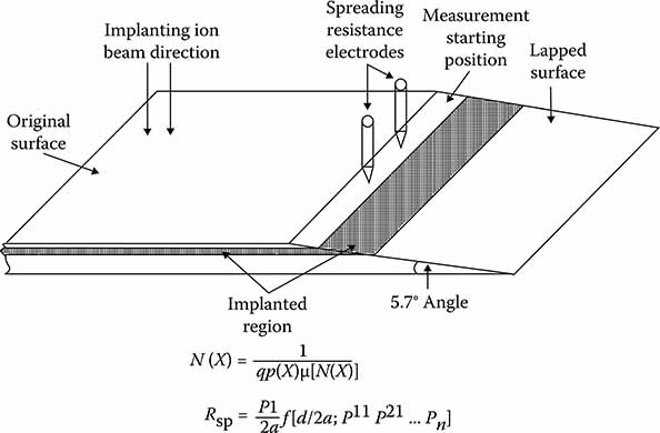
FIGURE 6.8
Spreading resistance measurement.
The expected resistivities for GaAs tests are much less than for silicon. They run from about 0.12 × 10⁻² to 8.8 × 10⁻² Ω-cm in undamaged and damaged regions, respectively. These values are calculated using values of electron mobility from Blakemore [8] and corresponding anticipated free carrier concentrations of between 1016 and 1018 cm−3. Under the assumption that the effective radius of the probe is 0.75 μm, the corresponding spreading resistance values range between 4 and 186 Ω. The following table illustrates these relations.
| Degree of Damage | None | Some | Full |
| Electron concentration (cm−3) | 1018 | 1017 | 1016 |
| Mobility (cm2/V/s) | 3300 | 5300 | 7100 |
| Resistivity (Ω-cm) | 0.19 × 10⁻² | 1.2 × 10⁻² | 8.8 × 10⁻² |
| Spreading resistance (Ω) | 4 | 25 | 186 |
There are several approaches which can be used in applying spreading resistance measurements to study damage in GaAs optical channel waveguides, for example. The easiest and most straightforward is to expose a separate unmasked sample of GaAs to the incident beam simultaneously with the exposure of the main pattern sample. The separate sample can then be sacrificed and studied separately. Alternatively, the separate sample could be a selected region on the main wafer, to be split off and studied separately. It is also possible, though more tedious, to sacrifice and study the actual channels with this method. The major difficulty is in achieving adequate alignment between the channel, the lapping edges, and the electrodes.
6.7 Mobility Measurement
Conwell and Weisskopf [9] determined a relationship between the carrier concentration in a semiconductor and the carrier mobility:
A differential four-point van der Pauw measurement (Figure 6.9) can be performed so that successive chemical etches of the wafer (each of known thickness) will provide u(d). The ND(d) information obtained with a Post Office profile provides
FIGURE 6.9
Van der Pauw measurement of resistivity and carrier mobility.
We then know both ND(d) and u(d), from which we can derive ND versus u.
An attractive experiment for measurement of the drift mobility of the carriers in implanted layers is the “time of flight” measurement. In this technique [10], “a relatively compact group of excess carriers, released or injected by some form of impulsive excitation, is caused by an externally applied electric field to traverse a known distance in more or less coherent fashion, and the time of its arrival is measured. In the absence of all diffusion, recombination, relaxation, and deep trapping effects, the drift mobility is given by μ = d/Eτ, where d is the known distance, E is the applied field, and τ is the observed transit time.” Techniques are currently under investigation to transform the experiment from the time domain to the frequency domain. It is believed that the “Fourier transform” method of drift mobility measurement will have practical advantages over the time-of-flight method.
6.8 Cross-Section Transmission Electron Microscopy
Microscopy is a very sensitive observational technique used to routinely investigate surface morphology and cleaved sections of multilayer structures. In conjunction with potassium hydroxide treatments, it allows the identification of large antiphase domains and stacking faults and the measurement of dislocation density.
This technique is often used to obtain the carrier distribution in implanted guides. It can potentially provide both transverse and longitudinal carrier distributions. Grinding and polishing are performed using a resin/semiconductor composite to reduce the sample thickness to 4–6 mils. Samples are then ion milled to ~2000 Å for TEM analysis and stacked so that the implanted layers are perpendicular to the plane of the sample.
In order to experimentally determine the location of implanted damage in GaAs, specimens are annealed prior to STEM. The annealing step allows defect migration and formation of extended line and loop defects which can be imaged by STEM. The post-anneal damage profile can then be delineated by calculating defect densities as a function of depth. Although the width of the peak damage region will be reduced somewhat by the anneal, the peak damage and end of range values will essentially remain unchanged.
6.9 Infrared Reflectivity Measurements
Infrared reflectivity of waveguides is often performed using a specular reflective attachment to a spectrophotometer [11]. The thickness of the waveguide is, to a good approximation, given by
where
s denotes the average spectral separation (in wave numbers) between maxima and minima in the fringe pattern
θ is the angle of incidence of the light rays
nf is the average value of the refractive index of the film (see Figure 6.10)
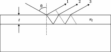
FIGURE 6.10
Interference measurement of dielectric film thickness.
6.10 Other Analysis Techniques
Angle polishing and staining is a technique enabling the observation of material layers down to a thickness on the order of 100 Å (see Figure 6.11). Surface profiling is accomplished with various profilometers. These devices allow routine assessment of surface roughness to a resolution of 0.1 μm. The electron microprobe is a device used to determine alloy composition of AlGaAs materials in the indirect band gap regime (i.e., for percentages of aluminum greater than approximately 45%). Hall and photo-Hall measurements yield information on material carrier density and mobility.
Deep-level transient spectroscopy (DLTS) and capacitance–transient (C-T) measurements are commonly used to provide a wide range of information on the electronic and optical defects in a material. These two capacitance techniques provide information on defect activation energy, capture cross section, and density. Figures 6.12 and 6.13 show the DLTS and C-T block diagrams.
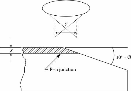
FIGURE 6.11
Measurement of junction depth by angle polishing and staining.
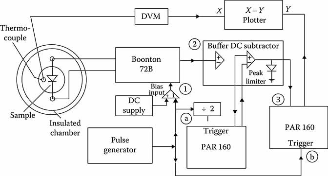
FIGURE 6.12
Block diagram of the DLTS measurement system.
Photoluminescence is an invaluable tool providing information on crystal uniformity, impurities, optical efficiency, and energy band gap for direct-gap semiconductors. The analysis of the half-width and intensity of AlGaAs system quantum well structures provides a very sensitive indication of the microscopic interface roughness of III–V heterostructures. Figure 6.14 shows the photoluminescence system block diagram.
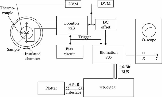
FIGURE 6.13
Block diagram of the C-T measurement system.
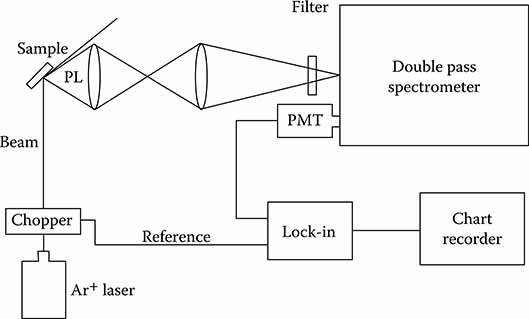
FIGURE 6.14
Photoluminescence system.
6.11 Biotechnology Applications
Na, K, and Cl are key ions inside and outside the cell, providing for fundamental cell function. Proteins with pump or channel features is now an accepted description for the mediating mechanism that regulates ion partitioning cellular function [12]. Receptor proteins may be closely linked to pump and channel proteins and may act to modulate their activity. Methods such as x-ray diffraction (see Chapter 7) provide valuable insights into protein structure and function. These are complemented by biological analysis tools such as sodium dodecylsulfate polyacrylamide gel electrophoresis (SDS-PAGE).
6.12 Parametric Analysis of Video
Video data analysis requires proper camera setup, timing, triggering, calibration, data acquisition, storage and transfer, and ultimate parametric analysis and reporting. This is accomplished in a seamless workflow with optimal efficiencies, ensuring digital image data is optimized for parametric analysis and event characterization. Ancillary technologies include advanced illumination techniques, including high brightness laser illumination, arc discharge lamp illumination, plasma lighting, structured lighting, and signal enhancement techniques. Custom MATLAB® routines are often employed for analysis of x-ray imagery. Specialized image acquisition methodologies are enhanced with data fusion from fiber-optic sensors and strain gauges, providing enhanced event characterization.
A typical process flow is illustrated in Figure 6.15 for an event employing, for example, high-speed video acquisition, x-ray cineradiography, surface deformation, and an integrated sensor suite. Event characterization may include analysis of impact velocity and velocity curves, pitch and yaw during trajectory and at impact, and deformation, providing correlation to a range of parameters.
A typical problem uses an image as an intermediate data structure, formed from raw data, which is analyzed further to extract desired information. This information—such as the location of a defect in a body armor image—can best be determined only after thoroughly understanding the physics of the imaging process and characterizing all available prior knowledge. Given this understanding, we develop signal processing algorithms that involve concepts from random signals, statistical inference, optimization theory, and digital signal processing [13].
A host of high-speed cameras are available commercially, including Vision Research Phantoms and Photron high-speed cameras (see Figure 6.16).
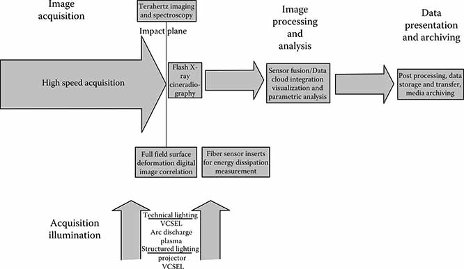
FIGURE 6.15
High-speed video acquisition process.
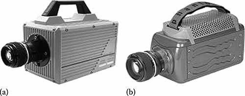
FIGURE 6.16
Representative high-speed video cameras. (a) Photron SA-5 (b) Vision Research V1.3.
6.12.1 Parametric Analysis of Digital Imagery
Digital image processing suites available for commercial licensing include ARAMIS, TrackEye, ProAnalyst, Correlated Solutions, PixelRay, and developmental MATLAB routines. Customized routines for specific test applications are available, along with data fusion processes for enhanced visualization and accuracy.
Two-dimensional parametric analysis requires a single imager with a calibration sample in the plane of motion either before or during the event. This provides measurement of 2-D flight characteristics such as pitch, yaw, position, velocity, and acceleration as well as angle, distance, and area, using the interactive feature tracking overlays. Distance and velocity, for example, gun bolt movement or the height an object moves into the air from a mine blast, are readily determined from 2-D imagery.
Three-dimensional (3-D) parametric analysis requires at least two imagers and a 3-D calibration fixture. This provides 3-D flight characteristics such as pitch, yaw, position, velocity, and acceleration as well as angle, distance, and area. Coordinate location and distance calculation for a traveling object are derived from the world reference points collected in a 3-D calibration. This is compared with time or fused with data from additional sensors.
Pitch and yaw for slugs and projectiles traversing a known path are calculated with a single 2-D image or, with 2 cameras, a 3-D image of the projectile flight.
Area and volume for smoke cloud or flash evaluation are performed in 2-D and utilize a 2-D calibration in the event plane. Volume measurements utilize 3-D analysis and calibration.
Surface deformation/3-D image correlation can be used for measurement of backface deformation during armor tests (exploitation). Surface deformation analysis utilizes a uniform random black and white speckle pattern on the surface and two calibrated high-speed cameras. Full field deformation analysis provides displacement and velocity in three coordinates, x–y strain, principal strain angle, in-plane rotation, 3-D contours, and curvature angles. Complementary solutions in development include projected structured lighting, laser illumination/bandpass filtering, and specialized illumination techniques.
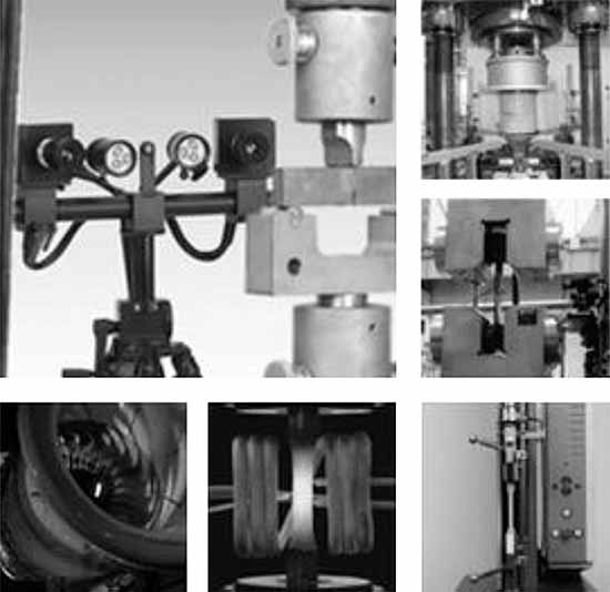
FIGURE 6.17
ARAMIS System. (Courtesy of Gesellschaft Für Optische Messtechnik [GOM] mbH, Braunschweig, Germany.)
An excellent example of optical 3-D measurement of surface deformation is the ARAMIS system produced by the Gesellschaft für Optische Messtechnik, GOM mbh (see Figure 6.17). Following is an excerpt from the GOM literature, illustrating the range of optical measurement capability for the 3-D software suite.
ARAMIS helps to better understand material and component behavior and is ideally suited to monitor experiments with high temporal and local resolution.
ARAMIS is a noncontact and material-independent measuring system providing, for static or dynamically loaded test objects, accurate
3-D surface coordinates
3-D displacements and velocities
Surface strain values (major and minor strain, thickness reduction)
Strain rates
ARAMIS is the ideal solution for
Determination of material properties (R- and N-values, FLC, Young’s Modulus, etc.)
Component analysis (crash tests, vibration analysis, durability studies, etc.)
Verification of finite element analysis
ARAMIS is the unique solution delivering complete 3-D surface, displacement and strain results where a large number of traditional measuring devices are required (strain gauges, LVDTs extensometers, etc.).
The same system setup is used for multiple applications and can be easily integrated in existing testing environments (see Figure 6.19).
6.12.1.1 CAD Data Integration
ARAMIS provides an import interface for CAD data, which are used for 3-D coordinate transformations and 3-D shape deviation calculations. (See Figure 6.18.)
The import interface handles the following formats:
Native: Catia v4/v5, UG, ProE
General: IGES, STL, VDA, STEP
6.12.1.2 Real-Time Data Processing
The ARAMIS software provides real-time results for multiple measurement positions from the test object’s surface.
These are directly transferred to testing devices, data acquisition units, or processing softwares (e.g., LabView, DIAdem, and MSExcel) and are used for
Controlling of testing devices
Long-term tests with smallest storage requirements
Vibration analysis
3-D video extensometer
6.12.1.3 Verification of FE Simulations
As part of complex process chains, optical measuring systems have become important tools in industrial processes in the last years. Together with the numerical simulation they have significant potential for quality improvement and optimization of development time for products and production.
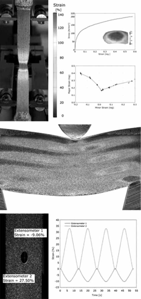
FIGURE 6.18
Representative parametric analysis visualizations. (Courtesy of Gesellschaft Für Optische Messtechnik [GOM] mbH, Braunschweig, Germany.)
ARAMIS strongly supports the full-field verification of FE-simulations. Determining material parameters with ARAMIS helps to evaluate and improve existing material models. The import of FE result datasets allows one to perform numerical full-field comparisons to FE simulations for all kinds of component tests. Thus finite element simulations can be optimized and are getting more reliable).
6.12.1.4 Complete Workflow in One Software Application
The entire measuring, evaluation and documentation process is carried out within the integrated ARAMIS software.
The full potential of the available hardware is used to capture and evaluate the measuring area efficiently and with high accuracy (see Figure 6.19).
6.13 X-Ray Imaging
X-ray imaging applications require unique optical detector system configurations for optimization of image quality, resolution, and contrast ratio. X-ray photons from multiple anode sources create a series of repetitive images on fast-decay scintillator screens, from which an intensified image is collected as a cineradiographic video (or intensified image) with high-speed videography Current developments address scintillator material formulation, flash x-ray implementation, image intensification, and high-speed video processing and display. Determination of optimal scintillator absorption, x-ray energy and dose relationships, contrast ratio determination, and test result interpretation are necessary for system optimization [14].
6.13.1 Introduction
Numerous test requirements motivate the development of flash x-ray cineradiography systems with multi-anode configuration for repetitive imaging in closely spaced timeframes. Applications include the following:
Shaped charge detonations to further understand properties of jet formation and particulation
Explosively formed projectile detonations to quantify launch and flight performance characteristics
Detonations of small caliber grenades and explosive projectiles to verify fuse function times and fragmentation patterns
Performance and behavior of various projectiles and explosive threats against passive, reactive, and active target systems
Human effects studies including body armor, helmets, and footwear

FIGURE 6.19
ARAMIS analysis system examples. (Courtesy of Gesellschaft Für Optische Messtechnik [GOM] mbH, Braunschweig, Germany.)Behind armor debris studies of large caliber ammunition against various armor materials
Small caliber projectile firings to study launch, free flight, and target impact results
Specific parameters of interest include impact velocity of projectiles striking various materials, pitch, yaw, and roll during projectile trajectory and at impact, time to maximum deformation of materials, time to final relaxation state, and profile of the deformation occurring during the events of interest.
6.13.2 Flash X-Ray
Flash x-ray is a well-established technology in which an electron beam diode (anode and cathode) in a sealed tube produces a brief (<30 ns) intense x-ray pulse. Recovery times are too slow to repetitively pulse the anode for high-speed cineradiography—high frame speed requires multiple independent pulsers and diodes. Sources are closely packed to minimize parallax problems and to maintain source intensity with smaller diodes [15]. Triggering of x-ray pulses is tailored to the event timing, so that precise imaging of the event is achievable with either high-speed framing cameras in which image frames are matched to the x-ray pulses, or high-speed video cameras with suitable exposure rates. Image processing algorithms are then utilized to allow extraction of parametric data from multiple frame x-ray images produced on scintillator screens and images through microchannel plate or image intensifier hybrids.
X-ray computed tomography (XCT) represents an alternative approach with the advantage of a 3-D image. The technique requires four or more pulsers for each 3-D frame, translating to 32 or more pulsers, to produce an equivalent eight frames [16]. There is no commercially available anode arrangement that lends itself to the correct geometry, and the cost of such a system would be substantial. For this reason, custom systems are constructed for specific applications.
6.13.3 Typical System Requirements
System specifications for cineradiography systems in development include the following:
Multi-anode x-ray system, 150–450 keV x-ray photons
Fluorescent screen/real-time video camera imaging, 6–8 foot standoff
One to five mm spot size, with 1 m2 target area
Up to 4 ms record time
Eight images at 100,000 frames per second, trigger synch pulses
Pulser repetition rate adjustable from 10,000 to 100,000 s−1
Independent inter-pulse time from anode to anode
Adaptable to a wide range of test scenarios/operation in harsh conditions/explosive test environment
Shown in Figure 6.20 is a multi-anode arrangement where the acquisition is achieved with a fast scintillator and a high-speed video camera. Multiple frames of imagery are produced on a scintillator screen by flash x-ray exposure through the test materials at either 150 or 450 keV. A turning mirror is used to avoid placement of the video camera directly in the residual x-ray beam. In a former approach, separate x-ray heads were used to image the event from different directions without overlap of the projection onto storage phosphor screens or x-ray film, from which still video images were obtained. This approach creates parallax and geometry issues, thus motivating the current approach in which successive frames are captured on a single area location on a scintillator screen. A framing camera with an image intensifier is synchronized with the x-ray pulses to capture snapshots over events of duration from tens of microseconds to a few milliseconds.
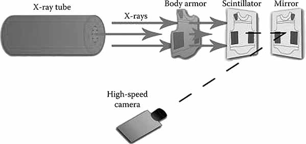
FIGURE 6.20
Typical multi-anode system configuration.
The choice between 150 and 450 keV x-rays represents a tradeoff between material penetration and contrast ratio. The attenuation coefficient for clay, for example, as reported by NIST [17] and Aberdeen, is 0.2 cm−1 at 450 keV and 0.3 cm−1 at 150 keV. For 10 in. of clay, the 150 keV flux is attenuated by about 15 X with respect to a 450 keV pulse. It is possible, using 450 keV x-rays and a storage phosphor screen, to image a 0.5 in. depression under the described angular alignment. The attenuation differential with x-ray energy implies a contrast ratio difference. As it is desirable to image depressions smaller than 0.5 in. (1.27 cm), with optimal resolution, the improved contrast ratio that obtains for 150 keV x-rays is an advantage—if the higher flux requirement can be accomodated.
6.13.4 Scintillators for Flash X-Ray
Six commercially available fast scintillators, from two manufacturers and one distributor, were characterized for efficiency and speed at 150 and 450 keV, as efficiency differences impact the increased flux requirements for imaging at 150 keV. No information on uniformity or sensitivity was available, and the speed of the samples deviated from data published in the literature. Availability, pricing, and timely delivery of suitable scintillators is expected to be a challenge associated with assembly of multiple systems.
The scintillators had various sizes up to about 6 in., so they were masked to have a common 6 mm diameter circular area from which light could be collected. Each was placed in a dark chamber with a fast photomultiplier tube module (Hamamatsu H9656MOD), containing a transimpedance amplifier. X-rays from the pulsers were directed at the scintillators from about 8 in. outside of the dark box, at a flux density of the order of 109 cm−2 and duration of approximately 30 ns/pulse. The photomultiplier was located about fourteen inches from the scintillator, and was followed by a Tektronix TDS 2024B 200 MHz 2 Gs/s oscilloscope. Photographs of the resulting traces were used to report the integrated output and speed of the scintillators.
It is interesting to note that the efficiency at 150 keV is not very different from that at 450 keV, despite the 7.4× higher attenuation reported in the literature for 150 keV with respect to 511 keV [17]. Future work around the visible photon yield per x-ray, as a function of x-ray energy and scintillator flavor, may help clarify the issue. It is also notable that the measured decay times are far longer than those reported [18]. For frames of about 1 μs duration, placed at various spacing throughout an event of tens to thousands of microseconds, the scintillator response times are inadequate.
6.13.5 System Configurations
Using currently available technology, the apparatus typically required in order to implement a flash cinematography system will likely include
High-voltage power supply
Trigger, timing, and delay control electronics
Trigger amplifier
X-ray pulser(s) + [1] multi-anode x-ray tube
Target positioning and backing fixture
High decay rate scintillating screen (<10 μs decay)
Mirror
Image intensifier
High frame rate camera
Computer control system and software
Connecting cables
This equipment can be configured in order to provide an efficient and safe means of capturing x-ray image sequences synchronized to high-velocity test events. The use of a multi-anode tube for x-ray exposure of fixed position targets will reduce the complexity of some test arrangements. Complete characterization of any parallax effects from multiple anode spacing can be used to enhance spatial resolution of images used for metrology. The imaging system selected for such a test configuration will require careful consideration of scintillating screen fluorescence, decay characteristics, and resolution limits. Similarly, the image intensifier resolution characteristics should be well matched to the system application. The camera utilized for image capture of the test sequence may be subject to upgrades as technical advances permit higher sensitivity and reduced exposure time.
Further development of flash x-ray cinematography includes the possibility of using directly illuminated CCD based detectors, UV scintillating screens, and x-ray diffraction apertures to control and/or reduce x-ray exposure regions [19,20]. Further advances in spatial metrology methods (such as point cloud algorithms) will further enhance the analytical capabilities for flash x-ray cinematography.
References
1. Developed by Boyd, J. University of Cincinnati. Private conversation with author.
2. Okamura, Y., S. Yoshinaka, and S. Yamamoto. 1983. Measuring mode propagation losses of integrated optical waveguides: A simple method. Appl. Opt. 22:3892.
3. Walker, R. G. 1985. Simple and accurate loss measurement techniques of semiconductor optical waveguides. Electron. Lett. 21:57.
4. See for example, Pankove, J. I. 1971. Optical Properties of Semiconductors. Englewood Cliffs, NJ: Prentice Hall, pp. 89–90.
5. Moss, T. S. 1959. Optical Properties of Semiconductors. New York: Butterworth, pp. 59–88.
6. Gooch, C. H. 1959. Gallium Arsenide Lasers. New York: Wiley-Interscience, p. 48.
7. Webster, G. 1983. Polaron Corporation. Private communication with author.
8. Blakemore, J. S. 1982. Semiconductor and other major properties of galluim arsenide. J. Appl. Phys. 53 (10):123.
9. Conwell, E. and V. F. Weisskopf. 1950. Theory of impurity scattering in semiconductors. Phys. Rev. 77:388.
10. Fagen, E. A. University of Delaware. 1984. Private conversation with author. Haynes, J. R. and W. Schockley. March 1951. The mobility and life of injected holes and electrons in germanium. Phys. Rev. 81:835–843.
11. Zavada, J. M., H. A. Jenkinson, T. J. Gavanis, R. G. Hunsperger, M. A. Mentzer, D. C. Larson, and J. Comas. 1980. Temperature processing effects in proton-implanted GaAs. Proceedings of SPIE 239. p. 157F.
12. Pollack, G. 2001. Cells, Gels and the Engines of Life. Seattle: Ebner and Sons Publishers.
13. Prince, J. L. and M. L. Jonathan. 2006. Medical Imaging, Signals and Systems. Upper Saddle River, NJ: Pearson Prentice Hall.
14. Mentzer, M. A., D. A. Herr, K. J. Brewer, N. Ojason, and H. A. Tarpine. January 2010. Detector development for x-ray imaging. Paper Presented at SPIE Photonics West, Sanfrancisco, CA.
15. Mattsson, A. 2007. New developments in flash radiography. Proceedings of SPIE 27th International Congress on High-Speed Photography and Photonics, China, 6279, 62790Z.
16. Karsten, M. and P. Helberg. 2005. Computed tomography of high-speed events. Proceedings of 22nd International Symposium on Ballistics 2, Vancouver, BC, Canada.
17. National Institute of Standards and Technology Physics Laboratory. 2010. Photon cross sections, attenuation coefficients, and energy absorptions coefficients from 10 keV to 100 GeV. NSRDS-NBS 29. U. S. Commerce Department. http://physics.nist.gov/PhysRefData/XrayMassCoef/ElemTab/z06.html
18. Shionoya, S. and W. M. Yen, eds. 1999. Phosphor Handbook. Boca Raton, FL: CRC Press.
19. Helberg, P., S. Nau, and K. Thoma. 2006. High-speed flash x-ray cinematography. ECNDT TH.1.3.2. Fraunhofer Institute for High Speed Dynamics, Ernst-Mach-Institut.
20. Cloens, P. September 18, 2006. X-Ray Imaging Instrumentation. ESRF, Grenoble, France.