
Theory
2.1 Theory of Electronics
This chapter covers the basic concepts of electronics, such as current, voltage, resistance, electrical power, capacitance, and inductance. After going through these concepts, this chapter illustrates how to mathematically model currents and voltage through and across basic electrical elements such as resistors, capacitors, and inductors. By using some fundamental laws and theorems, such as Ohm’s law, Kirchhoff’s laws, and Thevenin’s theorem, the chapter presents methods for analyzing complex networks containing resistors, capacitors, and inductors that are driven by a power source. The kinds of power sources used to drive these networks, as we will see, include direct current (dc) sources, alternating current (ac) sources (including sinusoidal and nonsinusoidal periodic sources), and nonsinusoidal nonperiodic sources. We will also discuss transient circuits, where sudden changes in state (such as flipping a switch within a circuit) are encountered. At the end of the chapter, the approach needed to analyze circuits that contain nonlinear elements (diodes, transistors, integrated circuits, etc.) is discussed.
I recommend using a circuit simulator program if you’re just starting out in electronics. The web-based simulator CircuitLab (www.circuitlab.com) is extremely easy to use and has a nice graphical interface. There are also online calculators that can help you with many of the calculations in this chapter. Using a simulator program as you go through this chapter will help crystallize your knowledge, while providing an intuitive understanding of circuit behavior. Be careful—simulators can lie, or at least they can appear to lie when you don’t understand all the necessary parameters the simulator needs to make a realistic simulation. It is always important to get your hands dirty—get out the breadboards, wires, resistors, power supplies, and so on, and construct. It is during this stage that you gain the greatest practical knowledge that is necessary for an inventor.
It is important to realize that components mentioned in this chapter are only “theoretically” explained. For example, in regard to capacitors, you’ll learn how a capacitor works, what characteristic equations are used to describe a capacitor under certain conditions, and various other basic tricks related to predicting basic behavior. To get important practical insight into capacitors, however, such as real-life capacitor applications (filtering, snubbing, oscillator design, etc.), what type of real capacitors exist, how these real capacitors differ in terms of nonideal characteristics, which capacitors work best for a particular application, and, more important, how to read a capacitor label, requires that you jump to Chap. 3, Section 3.6, which is dedicated to these issues. This applies to other components mentioned in this theory portion of the book.
The theoretical and practical information regarding transformers and nonlinear devices, such as diodes, transistors, and analog and digital integrated circuits (ICs), is not treated within this chapter. Transformers are discussed in full in Chap. 3, Section 3.8, while the various nonlinear devices are treated separately in the remaining chapters of this book.
A word of advice: if the math in a particular section of this chapter starts looking scary, don’t worry. As it turns out, most of the nasty math in this chapter is used to prove, say, a theorem or law or to give you an idea of how hard things can get if you do not use some mathematical tricks. The actual amount of math you will need to know to design most circuits is surprisingly small; in fact, basic algebra may be all you need to know. Therefore, when the math in a particular section in this chapter starts looking ugly, skim through the section until you locate the useful, nonugly formulas, rules, and so on, that do not have weird mathematical expressions in them. You don’t have to be a mathematical whiz to be able to design decent circuits.
2.2 Electric Current
Electric current is the total charge that passes through some cross-sectional area A per unit time. This cross-sectional area could represent a disk placed in a gas, plasma, or liquid, but in electronics, this cross-sectional area is most frequently a slice through a solid material, such as a conductor.
If ΔQ is the amount of charge passing through an area in a time interval Δt, then the average current Iave is defined as:
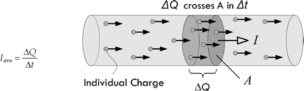
FIGURE 2.1
If the current changes with time, we define the instantaneous current I by taking the limit as Δt → 0, so that the current is the instantaneous rate at which charge passes through an area:
(2.1)
The unit of current is coulombs per second, but this unit is also called the ampere (A), named after Andre-Marie Ampere:
1 A = 1 C/s
To sound less nerdy, the term amp can be used in place of ampere. Because the ampere is a rather large unit, current is also expressed in milliamps (1 mA = 1 × 10⁻³ A), microamps (1 μA = 1 × 10⁻⁶ A), and nanoamps (1 nA = 1 × 10⁻⁹ A).
Within conductors such as copper, electrical current is made up of free electrons moving through a lattice of copper ions. Copper has one free electron per copper atom. The charge on a single electron is given by:
(2.2.a)
This is equal to, but opposite in sign of, the charge of a single copper ion. (The positive charge is a result of the atom donating one electron to the “sea” of free electrons randomly moving about the lattice. The loss of the electron means there is one more proton per atom than electrons.) The charge of a proton is:
(2.2.b)
The conductor, as a whole, is neutral, since there are equal numbers of electrons and protons. Using Eq. 2.2, we see that if a current of 1 A flows through a copper wire, the number of electrons flowing by a cross section of the wire in 1 s is equal to:
Now, there is a problem! How do we get a negative number of electrons flowing per second, as our result indicates? The only two possibilities for this would be to say that either electrons must be flowing in the opposite direction as the defined current, or positive charges must be moving in our wire instead of electrons to account for the sign. The last choice is an incorrect one, since experimental evidence exists to prove electrons are free to move, not positive charges, which are fixed in the lattice network of the conductor. (Note, however, there are media in which positive charge flow is possible, such as positive ion flow in liquids, gases, and plasmas.) It turns out that the first choice—namely, electrons flowing in the opposite direction as the defined current flow—is the correct answer.
Long ago, when Benjamin Franklin (often considered the father of electronics) was doing his pioneering work in early electronics, he had a convention of assigning positive charge signs to the mysterious (at that time) things that were moving and doing work. Sometime later, a physicist by the name of Joseph Thomson performed an experiment that isolated the mysterious moving charges. However, to measure and record his experiments, as well as to do his calculations, Thomson had to stick with using the only laws available to him—those formulated using Franklin’s positive currents. But these moving charges that Thomson found (which he called electrons) were moving in the opposite direction of the conventional current I used in the equations, or moving against convention. See Fig. 2.2.
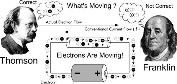
FIGURE 2.2 Thomson changed the notion that positive charges were what were moving in conductors, contrary to Franklin’s notion. However, negative electrons going one way is equivalent to positive charges going the opposite direction, so the old formulas still work. Since you deal with the old formulas, it’s practical to adopt Franklin’s conventional current—though realize that what’s actually moving in conductors is electrons.
What does this mean to us, to those of us not so interested in the detailed physics and such? Well, not too much. We could pretend that there were positive charges moving in the wires and various electrical devices, and everything would work out fine: negative electrons going one way are equivalent to positive charges going in the opposite direction. In fact, all the formulas used in electronics, such as Ohm’s law (V = IR), “pretend” that the current I is made up of positive charge carriers. We will always be stuck with this convention. In a nutshell, it’s convenient to pretend that positive charges are moving. So when you see the term electron flow, make sure you realize that the conventional current flow I is moving in the opposite direction. In a minute, we’ll discuss the microscopic goings-on within a conductor that will clarify things a bit better.
Example 1: How many electrons pass a given point in 3 s if a conductor is carrying a 2-A current?
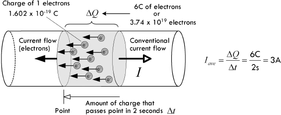
FIGURE 2.3
Answer: The charge that passes a given point in 3 s is:
ΔQ = I × Δt = (2 A)(3 s) = 6 C
One electron has a charge of 1.6 × 10⁻¹⁹ C, so 6 C worth of electrons is:
# Electrons = 6 C/1.602 × 10-19 C = 3.74 × 10¹⁹
Example 2: Charge is changing in a circuit with time according to Q(t) = (0.001 C) sin [(1000/s) t]. Calculate the instantaneous current flow.
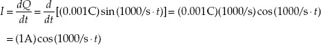
Answer: If we plug in a specific time within this equation, we get an instantaneous current for that time. For example, if t = 1, the current would be 0.174 A. At t = 3 s, the current would be − 0.5 A, the negative sign indicating that the current is in the opposite direction—a result of the sinusoidal nature.
Note: The last example involved using calculus—you can read about the basics of calculus in App. C if you’re unfamiliar with it. Fortunately, as we’ll see, rarely do you actually need to work in units of charge when doing electronics. Usually you worry only about current, which can be directly measured using an ammeter, or calculated by applying formulas that usually require no calculus whatsoever.
2.2.1 Currents in Perspective
What’s considered a lot or a little amount of current? It’s a good idea to have a gauge of comparison when you start tinkering with electronic devices. Here are some examples: a 100-W lightbulb draws about 1 A; a microwave draws 8 to 13 A; a laptop computer, 2 to 3 A; an electric fan, 1 A; a television, 1 to 3 A; a toaster, 7 to 10 A; a fluorescent light, 1 to 2 A; a radio/stereo, 1 to 4 A; a typical LED, 20 mA; a mobile (smart) phone accessing the web uses around 200 mA; an advanced low-power microchip (individual), a few μA to perhaps even several pA; an automobile starter, around 200 A; a lightning strike, around 1000 A; a sufficient amount of current to induce cardiac/respiratory arrest, around 100 mA to 1 A.
2.3 Voltage
To get electrical current to flow from one point to another, a voltage must exist between the two points. A voltage placed across a conductor gives rise to an electromotive force (EMF) that is responsible for giving all free electrons within the conductor a push.
As a technical note, before we begin, voltage is also referred to as a potential difference or just potential—they all mean the same thing. I’ll avoid using these terms, however, because it is easy to confuse them with the term potential energy, which is not the same thing.
A simple flashlight circuit, consisting of a battery connected to a lamp, through two conductors and a switch, is shown in Fig. 2.4. When the switch is open (“off”), no current will flow. The moment the switch is closed, however, the resistance of the switch falls to almost zero, and current will flow. This voltage then drives all free electrons, everywhere within the circuit, in a direction that points from negative to positive; conventional current flow, of course, points in the opposite direction (see Benjamin Franklin).
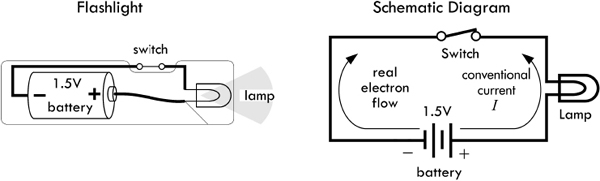
FIGURE 2.4
It is important to note that the battery needs the rest of the circuit, just as the rest of the circuit needs the battery. Without the linkage between its terminals, the chemical reactions within the battery cannot be carried out. These chemical reactions involve the transfer of electrons, which by intended design can only occur through a link between the battery’s terminals (e.g., where the circuit goes). Figure 2.5 shows this process using an alkaline dry cell battery. Notice that the flow of current is conserved through the circuit, even though the nature of the current throughout the circuit varies—ionic current within sections of the battery, electron current elsewhere.
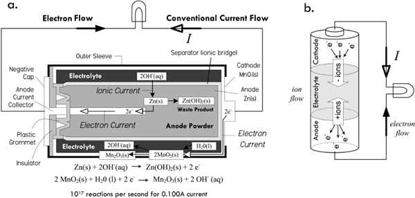
FIGURE 2.5
As free electrons within the lamp filament experience an EMF due to the applied voltage, the extra energy they gain is transferred to the filament lattice atoms, which result in heat (filament atomic vibrations) and emitted light (when a valence electron of a lattice atom is excited by a free electron and the bound electron returns to a lower energy configuration, thus releasing a photon).
A device that maintains a constant voltage across it terminals is called a direct current voltage source (or dc voltage source). A battery is an example of a dc voltage source. The schematic symbol for a battery is  .
.
To get a mental image of how a battery generates an EMF through a circuit, we envision that chemical reactions inside yield free electrons that quickly build in number within the negative terminal region (anode material), causing an electron concentration. This concentration is full of repulsive force (electrons repel) that can be viewed as a kind of “electrical pressure.” With a load (e.g., our flashlight lamp, conductors, switch) placed between the battery’s terminals, electrons from the battery’s negative terminal attempt to alleviate this pressure by dispersing into the circuit. These electrons increase the concentration of free electrons within the end of the conductor attached to the negative terminal. Even a small percentage difference in free electron concentration in one region gives rise to great repulsive forces between free electrons. The repulsive force is expressed as a seemingly instantaneous (close to the speed of light) pulse that travels throughout the circuit. Those free electrons nearest to the pumped-in electrons are quickly repulsed in the opposite direction; the next neighboring electrons get shoved, and so on down the line, causing a chain reaction, or pulse. This pulse travels down the conductor near the speed of light. See Fig. 2.6.
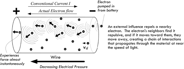
FIGURE 2.6
The actual physical movement of electrons is, on average, much slower. In fact, the drift velocity (average net velocity of electrons toward the positive terminal) is usually fractions of a millimeter per second—say, 0.002 mm/s for a 0.1-A current through a 12-gauge wire. We associate this drift movement of free electrons with current flow or, more precisely, conventional current flow I moving in the opposite direction. (As it turns out, the actual motion of electrons is quite complex, involving thermal effects, too—we’ll go over this in the next section.)
It is likely that those electrons farther “down in” the circuit will not feel the same level of repulsive force, since there may be quite a bit of material in the way which absorbs some of the repulsive energy flow emanating from the negative terminal (absorbing via electron-electron collisions, free electron–bond electron interactions, etc.). And, as you probably know, circuits can contain large numbers of components, some of which are buried deep within a complex network of pathways. It is possible to imagine that through some of these pathways the repulsive effects are reduced to a weak nudge. We associate these regions of “weak nudge” with regions of low “electrical pressure,” or voltage. Electrons in these regions have little potential to do work—they have low potential energy relative to those closer to the source of pumped-in electrons.
Voltage represents the difference in potential energy a unit charge has being at one location relative to another within a region of “electrical pressure”—the pressure attributed to new free electrons being pumped into the system. The relationship between the voltage and the difference in potential energy is expressed as:
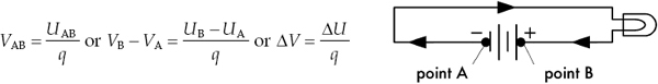
FIGURE 2.7
Implicit in the definition of voltage is the notion that voltage is always a measurement between two points, say point A and point B. That is the reason for the subscript “AB” in VAB. The symbol ΔV means the same. Both infer that there is an absolute scale on which to measure and give individual points a specific voltage value. In electronics, we can create such a scale by picking a point, often the point where there is the lowest electrical pressure, and defining this point as the zero point, or 0-V reference. In many dc circuits, people choose the negative terminal of the battery as the 0-V reference, and let everyone know by inserting a ground symbol  (more on this later). In practice, you rarely see voltages expressed using subscripts (VAB) or deltas (ΔV), but instead you simply see the symbol V, or you may see a symbol like VR. The “blank symbol” V, however, is always modified with a phrase stating the two points across which the voltage is present. In the second case, VR, the subscript means that the voltage is measured across the component R—in this case, a resistor. In light of this, we can write a cleaner expression for the voltage/potential energy expression:
Just make sure you remember that the voltage and potential energy variables represent the difference in relation to two points. As we’ll discover, all the big electronics laws usually assume that variables of voltage or energy are of this “clean form.”
In our flashlight example, we can calculate the difference in potential energy between an electron emanating from the negative terminal of the 1.5-V battery and one entering the positive terminal.
ΔU = ΔVq = (1.5 V)(1.602 × 10⁻¹⁹ C) = 2.4 × 10⁻¹⁹ J
Notice that this result gives us the potential energy difference between the two electrons, not the actual potential energy of either the electron emanating from the negative terminal (U1) or the electron entering the positive terminal (U0). However, if we make the assumption that the electron entering the positive terminal is at zero potential energy, we can figure that the electron emanating from the negative terminal has a relative potential energy of:
U1 = ΔU + U0 = ΔU + 0 = 2.4 × 10⁻¹⁹ J
Note: Increasing positive potential energy can be associated with similar charges getting closer together. Decreasing energy can be associated with similar charges getting farther apart. We avoided the use of a negative sign in front of the charge of the electron, because voltages are defined by a positive test charge. We are in a pickle similar to the one we saw with Benjamin Franklin’s positive charges. As long as we treat the potential relative to the pumped-in electron concentration, things work out.
In a real circuit, where the number of electrons pumped out by the battery will be quite large—hundreds to thousands of trillions of electrons, depending on the resistance to electron flow—we must multiply our previous calculation by the total number of entering electrons. For example, if our flashlight draws 0.1 A, there will be 6.24 × 10¹⁷ electrons pumped into it by the battery per second, so you calculate the potential energy of all the new electrons together to be about 0.15 J/s.
What about the potential energies of free electrons at other locations throughout the circuit, such as those found in the lamp filament, those in the positive wire, those in the negative wire, and so on? We can say that somewhere in the filament of the lamp, there is an electron that has half the potential energy of a fresh pumped-in electron emanating from the negative terminal of the battery. We attribute this lower energy to the fact that other free electrons up the line have lost energy due to collision mechanisms, which in turn yields a weaker electrical repulsive pressure (shoving action) that our electron in question experiences. In fact, in our flashlight circuit, we attribute all loss in electrical pressure to be through the lamp filament as free-electron energy is converted into heat and light.
In regard to potential energies of free electrons within the conductors leading to and from the battery, we assume all electrons within the same conductor have the same potential energy. This assumes that there is no voltage difference between points in the same conductor. For example, if you take a voltmeter and place it between any two points of a single conductor, it will measure 0 V. (See Fig. 2.8.) For practical purposes, we accept this as true. However, in reality it isn’t. There is a slight voltage drop through a conductor, and if we had a voltmeter that was extremely accurate we might measure a voltage drop of 0.00001 V or so, depending on the length of the conductor, current flow, and conductor material type. This is attributed to internal resistance within conductors—a topic we’ll cover in a moment.
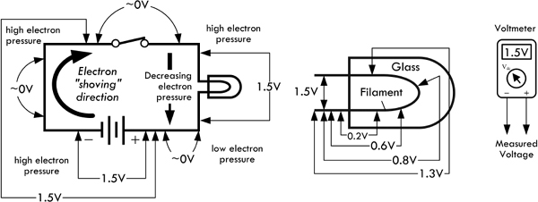
FIGURE 2.8
2.3.2 Definition of Volt and Generalized Power Law
We come now to a formal definition of the volt—the unit of measure of voltage. Using the relationship between voltage and potential energy difference V = U/q, we define a volt to be:
(Be aware that the use of “V” for both an algebraic quantity and a unit of voltage is a potential source of confusion in an expression like V = 1.5 V. The algebraic quantity is in italic.)
Two points with a voltage of 1 V between them have enough “pressure” to perform 1 J worth of work while moving 1 C worth of charge between the points. For example, an ideal 1.5-V battery is capable of moving 1 C of charge through a circuit while performing 1.5 J worth of work.
Another way to define a volt is in terms of power, which happens to be more useful in electronics. Power represents how much energy per second goes into powering a circuit. According to the conservation of energy, we can say the power used to drive a circuit must equal the power used by the circuit to do useful work plus the power wasted, as in the case of heat. Assuming that a single electron loses all its potential energy from going through a circuit from negative to positive terminal, we say, for the sake of argument, that all this energy must have been converted to work—useful and wasted (heat). By definition, power is mathematically expressed as dW/dt. If we substitute the potential energy expression U = Vq for W, assuming the voltage is constant (e.g., battery voltage), we get the following:
Since we know that current I = dq/dt, we can substitute this into the preceding expression to get:
(2.3)
This is referred to as the generalized power law. This law is incredibly powerful, and it provides a general result, one that is independent of type of material and of the nature of the charge movement. The unit of this electrical power is watts (W), with 1 W = 1 J/s, or in terms of volts and amps, 1 W = 1 VA.
The generalized power law can be used to determine the power loss of any circuit, given only the voltage applied across it and the current drawn, both of which can easily be measured using a voltmeter and an ammeter. However, it doesn’t tell you specifically how this power is used up—more on this when we get to resistance. See Fig. 2.9.
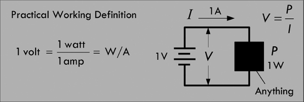
FIGURE 2.9
Example 1: Our 1.5-V flashlight circuit draws 0.1 A. How much power does the circuit consume?
Answer:
P = VI = (1.5 V)(0.1 A) = 0.15 W
Example 2: A 12-V electrical device is specified as consuming 100 W of power. How much current does it draw?
Answer:
2.3.3 Combining Batteries
To get a larger voltage capable of supplying more power, we can place two batteries in series (end to end), as shown in Fig. 2.10. The voltage across the combination is equal to the individual battery voltages added together. In essence, we have placed two charge pumps in series, increasing the effective electrical pressure. Chemically speaking, if the batteries are of the same voltage, we double the number of chemical reactions, doubling the number of electrons that can be pumped out into the circuit.
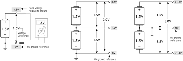
FIGURE 2.10
In Fig. 2.10, we use the notion of a ground reference, or 0-V reference, symbolized  . Though this symbol is used to represent an earth ground (which we define a bit later), it can also be used to indicate the point where all voltage measurements are to be referenced within a circuit. Logically, whenever you create a scale of measure, you pick the lowest point in the scale to be zero—0 V here. For most dc circuits, the ground reference point is usually placed at the negative terminal of the voltage source. With the notion of ground reference point, we also get the notion of a point voltage, which is the voltage measured between the ground reference and a specific point of interest within the circuit. For example, the single battery shown in Fig. 2.10 has a voltage of 1.5 V. We place a ground reference at the negative terminal and give this a 0-V point voltage, and place a 1.5-V point voltage marker at the positive terminal.
In the center of Fig. 2.10, we have two 1.5-V batteries in series, giving a combined voltage of 3.0 V. A ground placed at the negative terminal of the lower battery gives us point voltages of 1.5 V between the batteries, and 3.0 V at the positive terminal of the top battery. A load placed between ground and 3.0 V will result in a load current that returns to the lower battery’s negative terminal.
Finally, it is possible to create a split supply by simply repositioning the 0-V ground reference, placing it between the batteries. This creates +1.5 V and −1.5 V leads relative to the 0-V reference. Many circuits require both positive and negative voltage relative to a 0-V ground reference. In this case, the 0-V ground reference acts as a common return. This is often necessary, say, in an audio circuit, where signals are sinusoidal and alternate between positive and negative voltage relative to a 0-V reference.
2.3.4 Other Voltage Sources
There are other mechanisms besides the chemical reactions within batteries that give rise to an electromotive force that pushes electrons through circuits. Some examples include magnetic induction, photovoltaic action, thermoelectric effect, piezoelectric effect, and static electric effect. Magnetic induction (used in electrical generators) and photovoltaic action (used in photocells), along with chemical reactions, are, however, the only mechanisms of those listed that provide enough power to drive most circuits. The thermoelectric and piezoelectric effects are usually so small (mV range, typically) that they are limited to sensor-type applications. Static electric effect is based on giving objects, such as conductors and insulators, a surplus of charge. Though voltages can become very high between charged objects, if a circuit were connected between the objects, a dangerous discharge of current could flow, possibly damaging sensitive circuits. Also, once the discharge is complete—a matter of milliseconds—there is no more current to power the circuit. Static electricity is considered a nuisance in electrons, not a source of useful power. We’ll discuss all these different mechanisms in more detail throughout the book.
2.3.5 Water Analogies
It is often helpful to use a water analogy to explain voltage. In Fig. 2.11, we treat a dc voltage source as a water pump, wires like pipes, Benjamin Franklin’s positive charges as water, and conventional current flow like water flow. A load (resistor) is treated as a network of stationary force-absorbing particles that limit water flow. I’ll leave it to you to compare the similarities and differences.
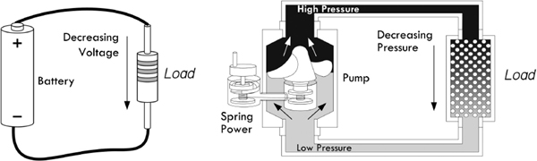
FIGURE 2.11
Here’s another water analogy that relies on gravity to provide the pressure. Though this analogy falls short of being accurate in many regards, it at least demonstrates how a larger voltage (greater water pressure) can result in greater current flow.
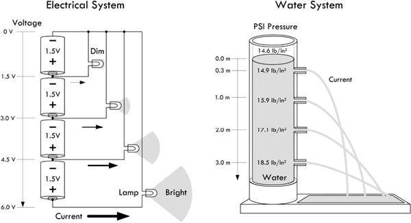
FIGURE 2.12
It’s not wise to focus too much attention on these water analogies—they fall short of being truly analogous to electric circuits. Take them with a grain of salt. The next section will prove how true this is.
Example 1: Find the voltage between the various points indicated in the following figures. For example, the voltage between points A and B in Fig. 2.13a is 12 V.
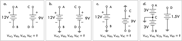
FIGURE 2.13
Answer: a. VAC = 0, VBD = 0, VAD = 0, VBC = 0. b. VAC = 3 V, VBD = 0 V, VAD = 12 V, VBC = 9 V. c. VAC = 12 V, VBD = −9V. VAD = −21V, VBC = 0 V. d. VAC = 3 V, VAB = 6 V, VCD = 1.5 V, VAD = 1.5 V, VBD = 4.5 V.
Example 2: Find the point voltages (referenced to ground) at the various locations indicated in the following figures.
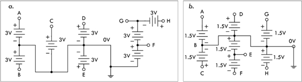
FIGURE 2.14
Answer: a. A = 3 V, B = −3 V, C = 3 V, D = 3 V, E = 3 V, F = 3 V, G = 6 V, H = 9 V. b. A = 1.5 V, B = 0 V, C = 1.5 V, D = 1.5 V, E = −1.5 V, F = −3.0 V, G = 1.5 V, H = −1.5 V.
2.4 A Microscopic View of Conduction (For Those Who Are Interested)
At a microscopic level, a copper conductor resembles a lattice of copper balls packed together in what’s called a face-centered-cubic lattice structure, as shown in Fig. 2.15. For copper, as well as other metals, the bonding mechanism that holds everything together is referred to as metallic bonding, where outermost valence electrons from the metal atoms form a “cloud of free electrons” which fill the space between the metal ions (positively charged atoms missing an electron that became “free”—see the planetary model in Fig. 2.15b). This cloud of free electrons acts as a glue, holding the lattice metal ions together.
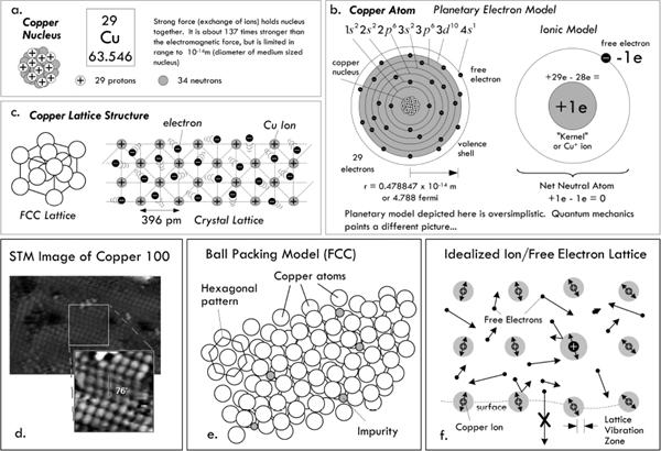
FIGURE 2.15 (a) Copper nucleus composed of protons and neutrons held together by nuclear forces that is roughly 137 times stronger than the electromagnetic force. (b) Copper atoms, as viewed by the classic planetary model, consisting of valance electrons held in orbit by electric forces. Quantum mechanics is required to explain why electrons exist in discrete energy levels, and why they don’t fall into the nucleus or radiate electromagnetic energy as they orbit. (c) Copper lattice has a face-centered cubic packing arrangement. (d) Scanning tunneling electron microscope (STM) image of copper 100, courtesy of Institut für Allgemeine Physik, TU Wien. (e) Ball packing model of lattice, showing irregularities in lattice geometry, partly caused by impurities (other kinds of atoms). (f) Lattice view showing that lattice atoms vibrate due to external thermal interactions as well as interactions with free electrons. Free electrons move about randomly, at varying speeds and directions, colliding with other electrons and lattice ions. Under normal conditions, they do not leave the surface of the metal.
Each free electron within the cloud of free electrons moves about in random directions and speeds, colliding and rebounding “off” metal ions and other imperfections (impurities in lattice and grain boundary transitions, etc.). It is important to realize that this is occurring in a chunk of copper, at room temperature, without any applied voltage.
At room temperature, no free electrons ever leave the surface of the metal. A free electron cannot escape the coulomb (electric) attractive forces presented by the positive metal ions in the lattice. (We’ll see later that under special conditions, using unique mechanisms, it is possible for electrons to escape.)
According to what’s called the free-electron model—a classical model that treats free electrons as a gas of noninteracting charges—there is approximately one free electron per copper atom, giving a copper conductor a free electron concentration of ρn = 8.5 × 1028 electrons/m3. This model predicts that, under normal conditions (a piece of copper just sitting there at room temperature), the thermal velocity v of electrons (or root-mean-square speed) within copper is about 120 km/s (1.2 × 10⁵ m/s), but depends on temperature. The average distance an electron travels before it collides with something, called the mean free path λ, is about 0.000003 mm (2.9 × 10⁻⁹ m), with the average time between collisions τ of roughly 0.000000000000024 s (2.4 × 10⁻¹⁴ s). The free-electron model is qualitatively correct in many respects, but isn’t as accurate as models based on quantum mechanics. (The speed, path, and time are related by v = λ/τ.)
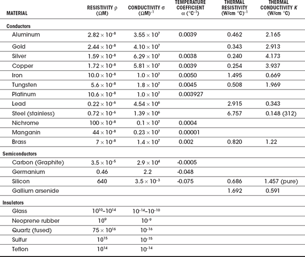
In quantum mechanics, electrons obey velocity-distribution laws based on quantum physics, and the movement of electrons depends on these quantum ideas. It requires that we treat electrons as though they were waves scattering from the lattice structure of the copper. The quantum view shows the thermal speed (now called Fermi velocity vF) of a free electron to be faster than that predicted by the free-electron model, now around 1.57 × 10⁶ m/s, and contrarily, it is essentially independent of temperature. In addition, the quantum model predicts a larger mean free path, now around 3.9 × 10⁻⁸ m, which is independent of temperature. The quantum view happens to be the accepted view, since it gives answers that match more precisely with experimental data. Table 2.1 shows the Fermi velocities of electrons for various metals.
TABLE 2.1 Condensed Matter Properties of Various Metals
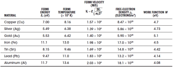
Note: 1 eV = 1.6022 × 10⁻¹⁹ J, me = 9.11 × 10⁻³¹ kg, c = 3.0 × 10⁸ m/s
Fermi energy and free electron density data from N.W. Ashcroft and N.D. Mermin, Solid State Physics, Saunders, 1976; work function data from Paul A. Tipler and Ralph A. Llewellyn, Modern Physics, 3rd ed., W.H. Freeman, 1999.
Also, the surface binding energy (caused by electrostatic attraction) that prevents electrons from exiting the surface of the metal, referred to as the work function, is about 4.7 eV for copper (1 eV = 1.6022 × 10⁻¹⁹ J). The only way to eject electrons is through special processes, such as thermionic emission, field emission, secondary emission, and photoelectric emission.
(Thermionic emission: increase in temperature provides free electrons enough energy to overcome work function of the material. The emitted electron is referred to as a thermoelectron. Field emission: additional energy from an electric field generated by a high-voltage conductor provides an attractive enough positive field to free electrons from the surface. This requires huge voltages [MV per cm between emitting surface and positive conductor]. Secondary emission: electrons are emitted from a metallic surface by the bombardment of high-speed electrons or other particles. Photoelectric emission: electron in material absorbs energy from incoming photon of particular frequency, giving it enough energy to overcome work function. A photon must be of the correct frequency, governed by W = hf0, for this to occur [Planck’s constant h = 6.63 × 10⁻³⁴ J-s or 4.14 × 10⁻¹⁴ eV; f0 is in hertz]).
2.4.1 Applying a Voltage
Next, we wish to see what happens when we apply a voltage across the conductor—say, by attaching a thick copper wire across a battery. When we do this, our randomly moving free electrons all experience a force pointing toward the positive end of the wire due to the electric field set up within the wire. (The field is due to the negative concentration of pumped-in electrons at one end relative to the neutral [positive relative to negative] concentration at the other end.) The actual influence this force has on the motion of the random free electrons is small—the thermal velocity is so large that it is difficult to change the momentum of the electrons. What you get is a slightly parabolic deviation in path, as shown in Fig. 2.16.
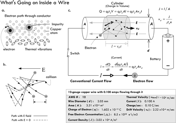
FIGURE 2.16 (a) Simplistic view of an electron randomly moving through a copper lattice, rebounding off lattice atoms and impurities. (b) An electron collides frequently with the ions and impurities in a metal and scatters randomly. In an electric field, the electron picks up a small component of velocity opposite the field. The differences in the paths are exaggerated. The electron’s path in an electric field is slightly parabolic. (c) Model illustrating current density, drift velocity, charge density, thermal velocity, and current.
Normally, the field present in the wire would create a net acceleration component in the direction of the force; however, the constant collisions electrons experience create a drag force, similar to the drag experienced by a parachute. The net effect is an average group velocity referred to as the drift velocity vd. Remarkably, this velocity is surprisingly small. For example, the voltage applied to a 12-gauge copper wire to yield a 0.100-A current will result in a drift velocity of about 0.002 mm per second! The drift velocity is related, determined by
vd = J/(ρee)
where J is the current density—the current flowing through an area (J = I/A), ρe is the free-electron density in the material, and e is the charge of an electron. Table 2.1 shows free-electron densities for various materials. As you can see, the drift velocity varies with current and diameter of the conductor.
The drift velocity is so slow, only fractions of a millimeter per second, that it is worth pondering how a measurable current can even flow. For example, what happens when you flip the switch on a flashlight? Of course, we don’t have to wait hours for electrons to move down the conductors from the battery. When we throw the switch, the electric field of the incoming electron has a repulsive effect on its neighbor within the wire. This neighbor then moves away toward another neighbor, creating a chain of interactions that propagates through the material at near the speed of light. (See Fig. 2.17.) This reaction, however, really isn’t the speed of light, but a fraction less, depending on the medium. The free electrons spreading throughout the conductor all start moving at once in response—those nearest the switch, as well as those nearest the light filament or LED. A similar effect occurs in fluid flow, as when you turn on a garden hose. Because if the hose is already full of water, the outflow starts immediately. The force of the water at the faucet end is quickly transmitted all along the hose, and the water at the open end of the hose flows almost at the moment the faucet is opened.
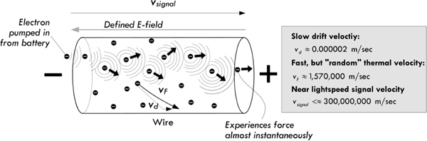
FIGURE 2.17 Illustration of how the electric field propagates down a wire as electrons are pumped into one end.
In the case of alternating current, the field reverses directions in a sinusoidal fashion, causing the drift velocity component of electrons to swish back and forth. If the alternating current has a frequency of 60 Hz, the velocity component would be vibrating back and forth 60 times a second. If our maximum drift velocity during an ac cycle is 0.002 mm/s, we could roughly determine that the distance between maximum swings in the drift distance would be about 0.00045 mm. Of course, this doesn’t mean that electrons are fixed in an oscillatory position. It means only that the drift displacement component of electrons is—if there is such a notion. Recall that an electron’s overall motion is quite random and its actual displacement quite large, due to the thermal effects.
2.5 Resistance, Resistivity, Conductivity
As was explained in the last section, free electrons in a copper wire at room temperature undergo frequent collisions with other electrons, lattice ions, and impurities within the lattice that limit their forward motion. We associate these microscopic mechanisms that impede electron flow with electrical resistance. In 1826, Georg Simon Ohm published experimental results regarding the resistance of different materials, using a qualitative approach that wasn’t concerned with the hidden mechanisms, but rather considered only the net observable effects. He found a linear relationship between how much current flowed through a material when a given voltage was applied across it. He defined the resistance to be the ratio of the applied voltage divided by the resultant current flow, given by:
(2.4)
This statement is called Ohm’s law, where R is the resistance, given in volts per ampere or ohms (abbreviated with the Greek symbol omega, Ω). One ohm is the resistance through which a current of 1 A flows when a voltage of 1 V is applied:
1 Ω = 1 V/1 A
The symbol  is used to designate a resistor.
Now, Ohm’s law isn’t really a law, but rather an empirical statement about the behavior of materials. In fact, there are some materials for which Ohm’s law actually doesn’t work.
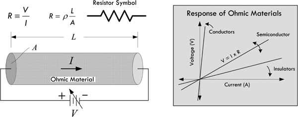
FIGURE 2.18
Ohm’s law can be applied only to ohmic materials—materials whose resistance remains constant over a range of voltages. Nonohmic materials, on the other hand, do not follow this pattern; they do not obey Ohm’s law. For example, a diode is a device that allows current to pass easily when the voltage is positive, but prevents current flow (creates a high resistance) when the voltage is negative.
CURIOUS NOTE ABOUT OHM’S LAW
Usually you see Ohm’s law written in the following form:
V = I × R
However, in this form it is tempting to define voltage in terms of resistance and current. It is important to realize that R is the resistance of an ohmic material and is independent of V in Ohm’s law. In fact, Ohm’s law does not say anything about voltage; rather, it defines resistance in terms of it and cannot be applied to other areas of physics such as static electricity, because there is no current flow. In other words, you don’t define voltage in terms of current and resistance; you define resistance in terms of voltage and current. That’s not to say that you can’t apply Ohm’s law to, say, predict what voltage must exist across a known resistance, given a measured current. In fact, this is done all the time in circuit analysis.
2.5.1 How the Shape of a Conductor Affects Resistance
The resistance of a conducting wire of a given material varies with its shape. Doubling the length of a wire doubles the resistance, allowing half the current to flow, assuming similar applied voltages. Conversely, doubling the cross-sectional area A has the opposite effect—the resistance is cut in half, and twice as much current will flow, again assuming similar applied voltages.
Increasing resistance with length can be explained by the fact that down the wire, there are more lattice ions and imperfections present for which an applied field (electric field instigated by added electrons pumped in by the source) must shove against. This field is less effective at moving electrons because as you go down the line, there are more electrons pushing back—there are more collisions occurring on average.
Decreasing resistance with cross-sectional area can be explained by the fact that a larger-volume conductor (greater cross-sectional area) can support a larger current flow. If you have a thin wire passing 0.100 A and a thick wire passing 0.100 A, the thinner wire must concentrate the 0.100 A through a small volume, while the thick wire can distribute this current over a greater volume. Electrons confined to a smaller volume tend to undergo a greater number of collisions with other electrons, lattice ions, and imperfections than a wire with a larger volume. The concentration of free-electron flow, according to Benjamin Franklin’s convention, represents a concentration of conventional current flow in the opposite direction. This concentration of current flow is called the current density J—the rate of current flows per unit area. For a wire: J = I/A. Figure 2.19 demonstrates how the current density is greater in a thin 12-gauge wire than in a thicker 4-gauge wire. It also shows that the drift velocity in the thick wire is less than the drift velocity in the thin wire—a result of a “decrease in electron field pressure” lowering the average “push” in the current flow direction.
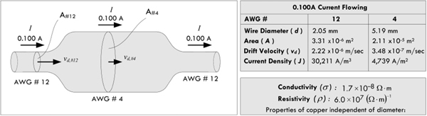
FIGURE 2.19 Effects of wire diameter on resistance. A thinner wire has more resistance per unit length than a thicker wire.
2.5.2 Resistivity and Conductivity
We have left out the most important aspect of resistance that has nothing to do with the physical length or diameter of the material. How does the “chemistry” of the material affect the resistance? For example, if you have a copper wire with the same dimensions as a brass wire, which metal has the greater overall resistance? To answer this question, as well as provide a way to categorize materials, we adopt the concept of resistivity. Unlike resistance, resistivity is entirely independent of the dimensions of the material. Resistivity is a property unique to the material. The resistivity ρ is defined as follows:
(2.5)
where A is the cross-sectional area, L is the length, and R is the overall resistance of the material, as measured across its length. The units of resistivity are ohm-meters (Ωm).
For some, resistivity is too negative a concept—it tells you how “bad” something is at passing current. Optimists prefer the concept of conductivity—how “good” something is at passing current. Conductivity, symbolized σ, is simply the mathematical inverse of resistivity:
(2.6)
The units of conductivity are siemens, S = (Ωm)−1. (Mathematical note: [Ωm]−1 = 1/[Ωm]). Both conductivity and resistivity contain the same important underlining information. Some prefer to play with equations that use the optimistic notion of conductivity (“glass half full”); others prefer the pessimistic notion of resistivity (“glass half empty”).
In terms of resistivity and conductivity, we can rewrite Ohm’s law as follows:
(2.7)
Table 2.2 shows the conductivities (resistivities, for the pessimists) of various materials. (Consult a technical handbook, such as The Handbook of Chemistry and Physics, for a more complete list.) The conductivity of metals, such as copper and silver, is a factor of 1021 higher than that of a good insulator, such as Teflon. Though both copper and silver are great conductors, silver is simply too expensive for practical use. Though aluminum is a fairly good conductor and was actually used at one time in home circuitry, it quickly became apparent that it oxidized badly, inhibiting good electrical contacts and limiting current flow to channels of limited size. The result produced fire hazards.
TABLE 2.2 Conductivity of Various Materials
An important feature of resistivity (or conductivity) is its temperature dependency. Generally, within a certain temperature range, the resistivity for a large number of metals obeys the following equation:
(2.8)
where ρ is the calculated resistivity based on a set reference resistivity ρ0 and temperature T0. Alpha α is called the temperature coefficient of resistivity, given in units of 1/°C or (°C)−1. The resistivity for most metals increases with temperature because lattice atom vibrations caused by thermal energy (increased temperature) impede the drift velocity of conducting electrons.
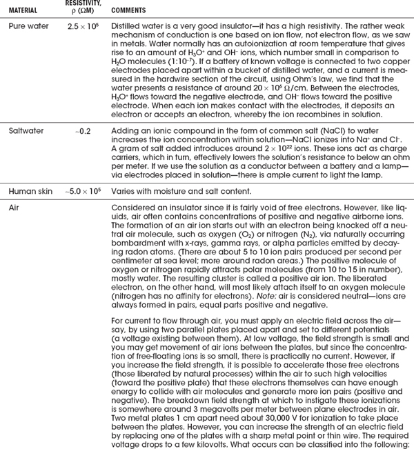
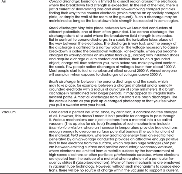
Are Water, Air, and Vacuums Considered Insulators or Conductors?
These media require special mention. See comments presented in Table 2.3.
TABLE 2.3 Resistivity of Special Materials
2.6 Insulators, Conductors, and Semiconductors
As we have seen, the electrical resistivities of materials vary greatly between conductors and insulators. A decent conductor has around 10−8 Ωm; a good insulator has around 1014 Ωm; a typical semiconductor from 10−5 to 103 Ωm—depending on temperature. What is the microscopic explanation for these differences?
The answer to this question rests upon the quantum nature of electrons. In classical physics the energy of an electron in a metal can take on any value—it is said the energy values form a continuum. (Here, electron energy is considered zero at infinite distance from the nucleus and becomes more negative in energy closer to the nucleus, relative to the zero reference state. Negative energy infers that there is electric attraction between the positive nucleus and the electron—it is electric potential energy.) However, a quantum description of electrons in metals shows that the energy values of electrons are quantized, taking on discrete values. This comes from the wavelike nature of electrons—analogous to standing waves on strings existing only at discrete frequencies. Figure 2.20 shows an energy diagram illustrating the possible energy levels of an electron (ignoring lattice influences). The diagram illustrates only the possible energy levels—electrons are not necessarily in each level.
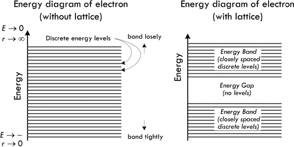
FIGURE 2.20 (Left) Energy diagram showing all possible energy levels of an electron in a solid; but it takes no account of the influence of an atomic crystalline lattice structure. (Right) Energy diagram that shows possible energy levels of an electron within a material made of a regular lattice of atoms. Electron energies are restricted to lie within allowed bands, and there is a large energy gap where no electrons are allowed. Even within the allowed bands, the possible electron energies are closely spaced discrete levels.
When a set of atoms forms a regular background lattice, the possible energy values of the electrons are altered even further. We still have discrete energy regions, called allowed bands, but we now get what are called energy gaps. Energy gaps are forbidden regions to the electron, and represent regions where no traveling wave (electron) can exist when placed in the periodic electric potential of the metal’s positive lattice ions. These gaps are quite large in the scale of atomic physics—within electron-volts range. Again, energy levels presented in the band diagram specify only possible values of electron energies—they may or may not be occupied.
Now, quantum physics has an interesting property, called the Pauli exclusion principle, which has a critical role in determining the properties of materials. The Pauli exclusion principle says that no two electrons in an atom can be in the same quantum state. The lowest common divisor of quantum states is the spin quantum number ms, which states that no more than two electrons with opposing spin (up or down) can be located in the same energy level. Now, if we consider a solid that has many free electrons, which is in an equilibrium state, electrons fill the lowest energy levels available in the allowed band, up to two in each level. Those electrons further down in energy are more tightly bound and are called innermost electrons. When all the electrons are placed in the lowest energy state, we are left with two possible outcomes. In the first case, the highest level to be filled is somewhere in the middle of a band. In the second case, the electrons just fill one or more bands completely. We assume that the material is at low enough temperature to prevent electrons from jumping to higher energy levels due to thermal effects.
Now if we add some energy to the free electrons by applying an electric field (attach a voltage source), for example, the electrons in the lower energy levels cannot accept that energy, because they cannot move into an already filled higher energy level. The only electrons that can accept energy are those that lie in the top levels, and then only if there are nearby empty levels into which they can move. Materials with electrons in only partly filled bands are conductors. When the top layer of their electrons moves freely into the empty energy levels immediately above, there is a current. The electrons that jump from a lower level to a higher level are said to be excited. The valance band is an allowed occupied band. The conduction band is an allowed empty band. The energy-band structure for conductors is shown in Fig. 2.21a and c.
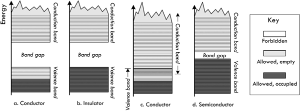
FIGURE 2.21 Four possible band structures for a solid: (a) Conductor—allowed band is only partially full, so electrons can be excited to nearby states. (b) Insulator—forbidden band with large energy gap between the filled band and the next allowed band. (c) Conductor—allowed bands overlap. (d) Semiconductor—energy gap between the filled band and the next allowed band is very small, so some electrons are excited to the conduction band at normal temperatures, leaving holes in the valence band.
If the highest-energy electrons of a material fill a band completely, then a small electric field will not give these electrons enough energy to jump the large energy gap to the bottom of the next (empty) band. We then have an insulator (see Fig. 2.21b). An example of a good insulator is diamond, whose energy gap is 6 eV.
In semiconductors, the highest-energy electrons fill a band (the valance band) at T = 0, as in insulators. However, unlike insulators, semiconductors have a small energy gap between that band and the next, the conduction band. Because the energy gap is so small, a modest electric field (or finite temperature) will allow electrons to jump the gap and thereby conduct electricity. Thus, there is a minimum electric field under the influence of which a material changes from insulator to conductor. Silicon and germanium have energy gaps of 1.1 eV and 0.7 eV, respectively, and are semiconductors. For semiconductors, an increase in temperature will give a fraction of the electrons enough thermal energy to jump the gap. For an ordinary conductor, a rise in temperature increases the resistivity, because the atoms, which are obstacles to electron flow, vibrate more vigorously. A temperature increase in a semiconductor allows more electrons into the empty band and thus lowers the resistivity.
When an electron in the valance band of a semiconductor crosses the energy gap and conducts electricity, it leaves behind what is known as a hole. Other electrons in the valence band near the top of the stack of energy levels can move into this hole, leaving behind their own holes, in which still other electrons can move, and so forth. The hole behaves like a positive charge that conducts electricity on its own as a positive charge carrier. An electron excited from the valence band to the conduction band is thus doubly effective at conducting electricity in semiconductors.
Besides the intrinsic elemental semiconductors, such as silicon and germanium, there are hybrid compounds—compounds such as gallium arsenide. Other semiconductors are made by introducing impurities into a silicon lattice. For example, an atom in the chemical group of phosphorous, arsenic, and antimony can replace one of the silicon atoms in a lattice without affecting the lattice itself too much. However, each of these impurities has one more electron in its valence level than the silicon atom has; this extra electron, for which there is no room in the valence band, takes a place in the conduction band and can conduct electricity. A semiconductor with impurities of this sort is called an n-type semiconductor, and the extra electrons are called donor electrons.
Atoms of elements in the same chemical group as boron, aluminum, and gallium have one less valence electron than silicon has. If an atom is added to a lattice of silicon as an impurity, there is one less electron than is needed to form a bond that holds the lattice together. This electron must be provided by the electrons of the valence band of the lattice material, and holes are created in this band. These holes act as positive charge carriers. The impurity atoms are called acceptors. A semiconductor with such impurities is called a p-type semiconductor.
We will see later on how n-type and p-type semiconductors are used for making one-way gates for current flow (diodes) and voltage-controlled current switches (transistors).
2.7 Heat and Power
In Sec. 2.3, we discovered the generalized power law, which tells us that if we can measure the current entering a device, as well as the voltage across the device, we know the power that is used by the device:
(2.9)
The generalized power law tells us how much power is pumped into a circuit but doesn’t say anything about how this power is used up. Let’s consider a two-lead black box—an unknown circuit that may contain all sorts of devices, such as resistors, lamps, motors, or transistors. If all we can do is measure the current entering the black box and the voltage across it—say, using an ammeter and voltmeter (or singularly, a wattmeter)—we could apply the generalized power law, multiply the measured current and voltage readings together, and find the power pumped into the black box. For example, in Fig. 2.22, we measure 0.1 A entering when a voltage of 10 V is applied, giving us a total consumed power of 1 W.
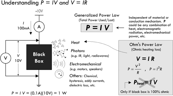
FIGURE 2.22
Knowing how much power is pumped into the black box is incredibly useful—it allows for quick power consumption measurements and often simplifies circuit analysis—as we’ll see later. But let’s say that we are interested in figuring out how much power is lost to heating (energy that goes into lattice vibrations, emissive radiation, etc.). We really can’t say, assuming we aren’t allowed to look inside the black box. There could be devices inside that take some of the initial energy and use it to do useful work, such as generating magnetic fields in the armature (rotor) and stator sections of a motor, causing the stator to rotate; or generating a magnetic field in a voice coil attached to a paper speaker cone that compresses air; or generating light energy, radio waves, and so on. There may be power converted into other weird forms not really coined as heat, such as driving chemical reactions, generating hysteresis effects, or eddy current in transformers.
The only time we can say for certain that power is totally converted into heat energy is if we assume our black box is a perfect resistor (100 percent ohmic in nature). Only then can we substitute Ohm’s law into the generalized power equation:
(2.10)
or
P = VI = (IR)I = I2R
In this form, the power lost due to heating is often called Ohmic heating, Joule heating, or I2R loss. Be careful how you interpret this law. For example, let’s consider our black box that drew 1 W of power. Given the power and the current—which we measure—it would be easy to assume that the resistance of the black box is:
Accordingly, we would say the black box is a 100-Ω resistor generating 1 W of heat. As you can see, this is an erroneous assumption, since we have disregarded the internal workings of the black box—we didn’t account for devices that perform useful work. You’ll often see people treat any load (black box) as a resistor when doing circuit analysis and such. This will get you the right answer when solving for a particular variable, but it is an analysis trick and shouldn’t be used to determine how much heat is being generated, unless, of course, the black box is actually a resistor.
The following example provides some insight into where power is being used and how much of it is being converted into heat.
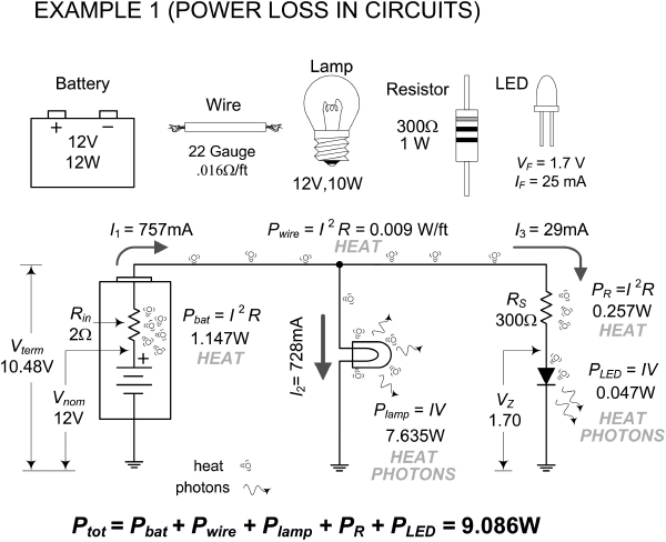
The total power pumped into this circuit gets converted into useful work and heat. The total “pump-in” power is:
Ptot = IV = (0.757 A)(12 V) = 9.08 W
(This is based on an open terminal battery measurement, without the rest of the circuit attached.) From there, we notice that some of the total power is wasted within the internal resistance of the battery, within the internal resistance of the wires, and within the resistance of the current-limiting resistor used by the LED. The power used to create light from the lamp and LED can be considered useful power used. However, since we can’t really separate the heat from the light power for these devices, we must apply the generalized power law to them and be content with that. According to the conservation of energy (or power), all individual powers within the circuit add up to the total power.
FIGURE 2.23
Example: With an ammeter and voltmeter, you measure the current drawn by a computer to be 1.5 A and the voltage entering to be 117 V. How much power does the computer consume? Can we say how much power is lost to heat?
Answer: P = IV = (1.5 A)(117 V) = 176 W. Knowing how much of the power is lost to heating is practically impossible to measure without taking the computer apart.
Example: Determine the resistance of the following four round rods of material, each 1 m long and 2 mm in diameter: copper, brass, stainless steel, and graphite. Also figure out how much power is lost to heating if a current of 0.2 A flows through each one.
Answer: Using Eq. (2.5),
Using Table 2.2:
ρcopper = 1.72 × 10⁻⁸ Ωm, ρbrass = 7.0 × 10⁻⁸ Ωm, ρsteel = 7.2 × 10⁻⁷ Ωm, ρgraphite = 3.5 × 10⁻⁵ Ωm
Substituting this into the resistance expression, we get:
Rcopper = 5.48 × 10⁻³ Ω, Rbrass = 2.23 × 10⁻² Ω, Rsteel = 2.31 × 10⁻¹ Ω, Rgraphite = 11.1 Ω
The power loss we get by using Eq. 2.10: P = I2R = (0.2 A)2R = (0.04 A2)R:
Pcopper = 2.2 × 10⁻⁴ W, Pbrass = 8.9 × 10⁻⁴ W, Psteel = 9.2 × 10⁻³ W, Pgraphite = 0.44 W
2.8 Thermal Heat Conduction and Thermal Resistance
How is the energy transferred in heating? Within a gas, heat transfer represents the transfer of energy between colliding gas molecules. Gas molecules at a hotter temperature move around more quickly—they have a high kinetic energy. When they are introduced into another, colder-temperature gas, the “hotter,” fast-moving molecules impart their energy to the slower-moving molecules. Gases tend to be the worst thermal conductors, due to a low density of molecules.
In nonmetals, heat transfer is a result of the transfer of energy due to lattice vibrations—energetically vibrating atoms in one region of a solid (e.g., the region near a flame) transfer their energy to other regions of a solid that have less energetically vibrating atoms. The transfer of heat can be enhanced by cooperative motion in the form of propagating lattice waves, which in the quantum limit are quantized as phonons. The thermal conductivity of nonmetals varies, depending greatly on the lattice structure.
In terms of metals, heat transfer is a result of both lattice vibration effects (as seen in nonmetals) as well as kinetic energy transfer due to mobile free electrons. Recall that free electrons within a metal are moving quite fast (~106 m/s for most metals) at room temperature. Though quantum mechanics is required, it is possible to treat these electrons like a dense gas, capable of increasing its overall energy as heat is added, and likewise, capable of transporting this energy to regions of the metal that are lower in temperature. Notice, however, that an increase in metal temperature, as a whole, also increases the electrical resistance—the drift velocity component of the free electron goes down, due to both increased lattice vibrations and an increase in thermal velocity component. It becomes harder to influence the free electrons with an applied field. Metals are the best thermal conductors, due in part to the additional free electrons.
The energy an object has at temperature T is correlated to the internal energy—a result of its internal atomic/molecular/electron motions. It is not correct, however, to use the word heat, such as “object possesses heat.” Heat is reserved to describe the process of energy transfer from a high-temperature object to a lower-temperature object. According to the first law of thermodynamics, which is a statement about the conservation of energy, the change in internal energy of a system ΔU is equal to the heat QH added to the system and the work W done by the system: ΔU = QH − W. If we assume that no work is done (energy transferred to, say, move a piston, in the case of a gas), we say ΔU = QH. With this assumption, we can take heat to be not a measure of internal energy of the system, but a change in internal energy. The main reason for this concept is that it is very difficult to determine the actual internal energy of a system; changes in internal energy are more meaningful and measurable.
In practice, what is most useful is the rate of heat transfer—the power loss due to heating. With the help of experimental data, the following formula can be used to determine how well certain materials transfer heat:
(2.11)
Here, k is called the thermal conductivity (measured in W/m °C) of the material in question, and ∇T is the temperature gradient:
Now, the gradient is probably scary to a lot of you—it is simply a way to represent temperature distributions in 3-D, with time. To keep things simple, we will stick to 2-D, and represent the gradient as acting through an area A through a thickness L, and assume steady-state conditions:
(2.12)
where ΔT = Thot − Tcold, measured at points across the length L of the material. The material may be steel, silicon, copper, PC board material, and so on. Figure 2.24 shows a picture of the situation.
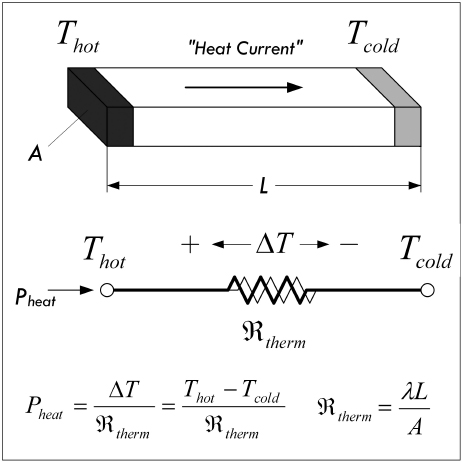
When one end of a block of material is placed at a hot temperature, heat will be conducted through the material to the colder end. The rate of heat transfer, or power due to heating, depends on the thermal resistance of the material, which in turn is dependent on the geometry of the material and the material’s thermal resistivity. A weird-looking resistor-like symbol is used here to represent the thermal resistance. Table 2.4 shows the thermal resistivities of various materials.
FIGURE 2.24
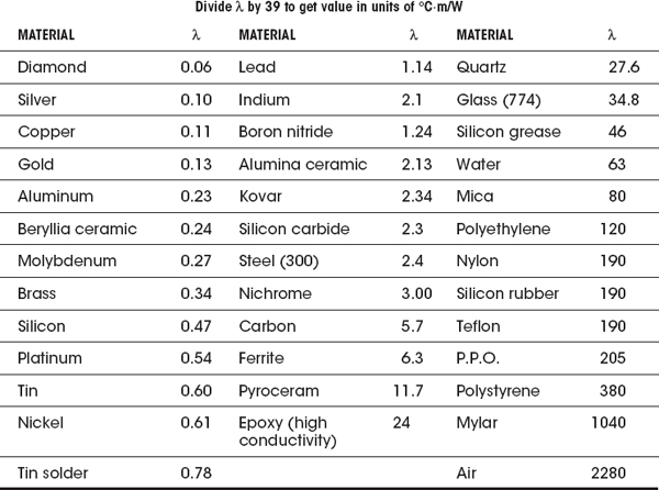
Thermal conductivity k, like electrical conductivity, has an inverse—namely, thermal resistivity λ. Again, one tells you “how good” a material is at transferring heat, the other tells you “how bad” it is at doing it. The two are related by k = 1/λ.
If we consider the geometry of the material, we can create a notion of thermal resistance ℜtherm (analogous to electrical resistance), which depends on the cross-sectional area A, the length of the block of material L, and the thermal conductivity k, or resistivity λ:
(2.13)
Thermal resistance has units of °C/W.
Thus, putting everything together, the power transfer of heat across a block of material, from one point at one temperature to another point at a different temperature, can be expressed as:
(2.14)
(k = thermal conductance) (λ = thermal resistivity) (ℜtherm = thermal resistance)
A very useful property of Eq. 2.14 is that it is exactly analogous to Ohm’s law, and therefore the same principles and methods apply to heat flow problems as to circuit problems. For example, the following correspondences hold:
Electrical conductivity σ [S/m or (Ωm)−1] |
|
Thermal resistivity λ [m°C/W] |
Electrical resistivity ρ [Ωm] |
Thermal resistance ℜtherm [°C/W] |
Electrical resistance R [Ω] |
Thermal current (heat flow) Pheat [W] |
Electrical current I [A] |
Thermal potential difference ΔT [°C] |
Electrical potential difference or voltage V [V] |
Heat source |
Current source |
Example: Calculate the temperature of a 4-in (0.1 m) piece of #12 copper wire at the end that is being heated by a 25-W (input power) soldering iron, and whose other end is clamped to a large metal vise (assume an infinite heat sink), if the ambient temperature is 25°C (77°F).
Answer: First, calculate the thermal resistance of the copper wire (diameter #12 wire is 2.053 mm, cross-sectional area is 3.31 × 10⁻⁶ m2):
Then, rearranging the heat flow equation and making a realistic assumption that only around 10 W of heat actually is transferred to the wire from the 25-watt iron, we get:
ΔT = Pheatℜtherm = (10 W)(77.4°C/W) = 774°C
So the wire temperature at the hot end is estimated at:
25°C + ΔT = 799°C (or 1470°F)
It’s important to realize that in the preceding example, we assume steady-state conditions, where the soldering iron has been held in place for a long time. Also, the assumption that only 10 W were transferred is an important point, since there is a lot of heat being radiated off as heat to the air and the iron handle, and so on. In any case, things can get very hot, even when moderate power levels are in question.
2.8.1 Importance of Heat Production
Heat production has its place in electronics (toasters, hair dryers, water heaters, etc.), but most of the time heat represents power loss that is to be minimized whenever possible, or at least taken into consideration when selecting components. All real circuit components—not just resistors but things like capacitors, transformers, transistors, and motors—contain inherent internal resistances. Though these internal resistances can often be neglected, in some situations they cannot be ignored.
Major problems arise when unintended heat generation increases the temperature of a circuit component to a critical point, causing component failure by explosion, melting, or some other catastrophic event. Less severe problems may surface as a component becomes thermally damaged, resulting in a change in characteristic properties, such as a shift in resistance that may cause undesirable effects in circuit behavior.
To avoid problems associated with heat production, it’s important to use components that are rated to handle two to three or more times the maximum power they are expected to dissipate. In cases where heat presents a shift in component parameter performance, selecting a component with a lower temperature coefficient (TC) will help.
Heat dissipation (more correctly, the efficient removal of generated heat) becomes very important in medium-to high-power circuits—power supplies, amplifier stages, transmitting circuits, and power-hungry circuits with power transistors. There are various techniques to remove heat from a circuit in order to lower the operating temperature of components to below critical levels. Passive methods include heat sinks, careful component layout, and ventilation. Heat sinks are special devices that are used to draw heat away from temperature-sensitive devices by increasing the radiating surface in air—which acts like a cooling fluid for conduction. Active methods include forced air (fans) or some sort of liquid cooling. We’ll discuss these methods throughout the book.
Example: Figure 2.25 shows a thin-film resistor in an integrated circuit. How hot will it get with 2 W dissipated over its 0.1 × 0.2-in surface (100 W/in2)? Assume the ground plane is at 80°C.
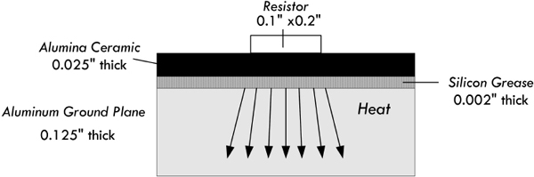
FIGURE 2.25
Answer: Since we have three different media through which this heat will be transferred, we must take into consideration thermal conduction within each. With the help of Eq. 2.14 and Table 2.4, we get the individual heat transfers through each region:
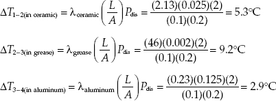
Adding this together:
ΔT1–4 = 5.3°C + 9.2°C + 2.9°C = 17.4°C
Adding this to the 80°C for the aluminum ground plane leads to an estimated 100°C for maximum resistor temperature. This is a conservative estimate, since it neglects transverse heat spreading.
In Sec. 2.5, we saw that the current density within a copper wire increased as the diameter of the wire decreased. As it turns out, a higher current density translates into a hotter wire; there are more collisions occurring between electrons and copper lattice ions. There is a point where the current density can become so large that the vibrating effect can overpower the copper-lattice binding energy, resulting in wire meltdown (also referred to as the fusing point). To prevent this from occurring, it is important to select the appropriate wire size for anticipated current levels. Wire size is expressed in gauge number—the common standard being the American Wire Gauge (AWG)—whereby a smaller gauge number corresponds to a larger-diameter wire (high current capacity). Table 2.5 shows a short list of common AWG wires. Section 3.1, on wires and cables, provides a more in-depth list.
TABLE 2.5 Copper Wire Specifications (Bare and Enamel-Coated Wire)
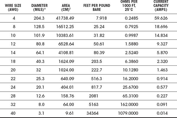
* 1 mil = 0.001 in or 0.0254 mm.
† A circular mil (CM) is a unit of area equal to that of a 1-mil-diameter circle. The CM area of a wire is the square of the mil diameter.
Diameters of wires in Fig. 2.26 are relative and not to scale.
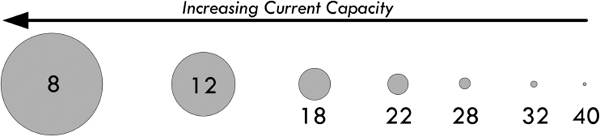
FIGURE 2.26
Example: A load device that is known to vary in output power from 0.1 mW to 5 W is to be connected to a 12-V source that is 10 ft away from the load. Determine the minimum wire gauge, provided by Table 2.5, that can safely support any anticipated current drawn by the load.
Answer: We only care about the maximum power level, so using the generalized power law:
Given only the selection of wire gauges provided by Table 2.5, a 22-gauge wire with a 0.914-A rating would work, though we could be conservative and select an 18-gauge wire with a 2.32-A rating. Since the length is so short, there is no appreciable drop in voltage through the wire, so we can ignore the length.
Example: A 10-Ω heating device is powered by a 120-VAC source. How much current does it draw, and what size conductors should be used to connect to the device?
Answer: 120 VAC is an RMS value of a sinusoidal voltage—in this case, household line voltage. Though we’ll discuss this later when we cover ac, it can be treated like a dc voltage in terms of power dissipated through a resistor. So,
A 10-gauge wire would support this kind of current, though a larger 8-gauge wire would be safer.
Example: Why shouldn’t you connect a wire across a voltage source? For example, if you connect a 12-gauge wire directly across a 120-V source (120-V mains outlet), what do you think will happen? What will happen when you do this to a 12-V dc supply, or to a 1.5-V battery?
Answer: In the 120-V mains case, you will likely cause a huge spark, possibly melting the wire and perhaps in the process receiving a nasty shock (if the wire isn’t insulated). But more likely, your circuit breaker in the home will trip, since the wire will draw a huge current due to its low resistance—breakers trip when they sense a large level of current flowing into one of their runs. Some are rated at 10 A, others at 15 A, depending on setup. In a good dc supply, you will probably trip an internal breaker or blow a fuse, or in a bad supply, ruin the inner circuitry. In the case of a battery, there is internal resistance in the battery, which will result in heating of the battery. There will be less severe levels of current due to the internal resistance of the battery, but the battery will soon drain, possibly even destroying the battery, or in an extreme case causing the battery to rupture.
2.10 Grounds
As we left off in Sec. 2.3, we saw that understanding voltage is a relativity game. For example, to say that a point in a circuit has a voltage of 10 V is meaningless unless you have another point in the circuit with which to compare it. Often you define a point in the circuit to be a kind of 0-V reference point on which to base all other voltage measurements. This point is often called the ground, and is frequently represented by the symbol shown in Fig. 2.27:
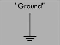
FIGURE 2.27
For example, Fig. 2.28 shows various ways in which to define voltages by selecting a ground—which in this case is simply a 0-V reference marker. The single battery provides a 1.5-V potential difference or voltage between its terminals. We can simply place a 0-V reference ground at the negative terminal and then state that the positive terminal sits at 1.5 V relative to the 0-V reference ground. The 0-V reference, or the negative terminal of the battery, is called the return. If a load, such as a lamp or resistor, is placed between the terminals, a load current will return to the negative terminal.
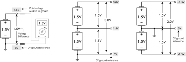
FIGURE 2.28
In the center diagram in Fig. 2.28, we have two 1.5-V batteries placed end to end. When batteries are linked this way, their voltages add, creating a combined total voltage of 3.0 V. With the 0-V reference ground at the bottom, we get 1.5-V and 3.0-V readings at the locations shown in the figure. A load placed across the two batteries (3.0-V difference) will result in a load current that returns to the lower battery’s negative terminal. In this case, the return is through the 0-V reference—the lower battery’s negative terminal.
Finally, it is possible to create a split supply by simply repositioning the 0-V ground reference, placing it between the batteries. This creates +1.5 V and −1.5 V leads relative to the 0-V reference. Many circuits require both positive and negative voltage relative to a 0-V ground reference. In this case, the 0-V ground reference acts as a common return. This is often necessary—say, in an audio circuit—where signals are sinusoidal and alternate between positive and negative voltage relative to a 0-V reference.
Now, the ground symbol shown in Fig. 2.27 as a 0-V reference, or as a return, is used all the time by various people. As it turns out, however, it really is supposed to represent a true earth ground—a physical connection to the earth through a conductive material buried in the earth. For whatever reasons, the symbol’s dual meaning has survived, and this can often be a source of confusion to beginners.
2.10.1 Earth Ground
The correct definition of an earth ground is usually a connection terminated at a rod driven into the earth to a depth of 8 ft or more. This earth ground rod is wired directly to a mains breaker box’s ground bar and sent to the various ac outlets in one’s home via a green-coated or bare copper wire that is housed within the same mains cable as hot and neutral wires. The ground can then be accessed at the outlet at the ground socket. Metal piping buried in the earth is often considered an earth ground. See Fig. 2.29.
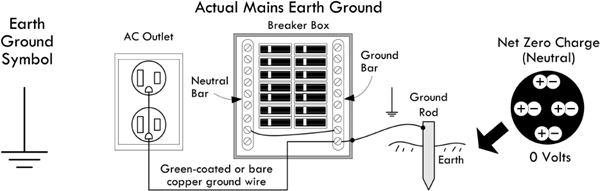
FIGURE 2.29 Earth ground.
A physical link to the earth is important because the earth provides an electrically neutral body; equal numbers of positive and negative charges are distributed through its entirety. Due to the earth’s practically infinite charge neutrality, attempts at changing the earth potential, via electrical generators, batteries, static electrical mechanisms, or the like, will have essentially no measurable effect. Any introduction of new charge into the earth is quickly absorbed (the earth’s moist soil is usually rather conductive). Such charge interactions occur constantly throughout the planet, and the exchanges average out to zero net charge.
For practical purposes, then, the earth is defined to be at a zero potential (relative to other things)—a potential that is practically immune to wavering. This makes the earth a convenient and useful potential on which to reference other signals. By connecting various pieces of electronics equipment to the earth ground, they can all share the earth’s ground reference potential, and thus all devices share a common reference.
The actual physical connection to earth ground at a particular piece of equipment is usually through the power cord’s ground wire that links to the mains ground wire network when the device is plugged in. The ground wire from the power cord is typically connected internally to the equipment chassis (frame) and, more important for our discussion, to the return portion of a channel that emanates from the interior circuitry. This is then brought out as a ground lead terminal. For example, in Fig. 2.30, an oscilloscope, function generator, and generic audiovisual device use BNC and UHF connectors for input and output channels. Internally, the outer connector body of the BNC or UHF jack is wired to the return (or source) portion of the channel, while a central conductor wire (insulated from the outer body) is wired to the source (or return) portion of the channel. The important part, now, is that the return, or outer, connector is also internally wired to the mains ground wire through the power cord cable. This sets the return to an earth ground reference. In the case of the dc power supply, a separate earth ground terminal is presented at the face in the form of a banana jack terminal. In order to ground the dc supply, a jumper wire must be connected between the negative supply terminal and the ground terminal. If no jumper is used, the supply is said to be floating.
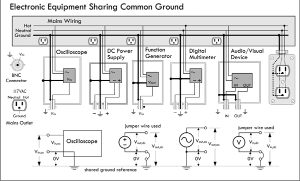
FIGURE 2.30 Illustration showing how various test instruments and an audiovisual device share a common ground connection through the mains ground wiring.
All the grounded pieces of equipment share a common ground. To prove this to yourself, try measuring the resistance between the ground terminals of any two separate pieces of test equipment in your lab. If the devices are properly grounded, you will get a measurement of 0 Ω (but a bit more for internal resistances).
Besides acting simply as a reference point, grounding reduces the possibility of electrical shock if something within a piece of equipment should fail and the chassis or cabinet becomes “hot.” If the chassis is connected to a properly grounded outlet via a three-wire electrical system ground, the path of current flow from the hot chassis will be toward ground, not through your body (which is a more resistive path). A ground system to prevent shock is generally referred to as a dc ground. We’ll discuss shock hazards and grounding later, when we cover ac.
Grounding also helps eliminate electrostatic discharge (ESD) when a statically charged body comes in contact with sensitive equipment. The charged body could be you, after a stroll you took across the carpet. Some ICs are highly vulnerable to damage from ESD. By providing a grounded work mat or using a grounded wrist strap while working with sensitive ICs, you can avoid destroying your chips by ensuring that charge is drained from your body before you touch anything.
Another big job the ground system does is provide a low-impedance path to ground for any stray RF current caused by stray radiofrequency-producing devices, such as electrical equipment, radio waves, and so on. Stray RF can cause equipment to malfunction and contributes to RFI problems. This low-impedance path is usually called RF ground. In most cases, the dc ground and the RF ground are provided by the same system.
Common Grounding Error
As previously mentioned, the ground symbol, in many cases, has been used as a generic symbol in circuit diagrams to represent the current return path, even though no physical earth ground is used. This can be confusing for beginners when they approach a three-terminal dc power supply that has a positive (+), negative (-), and ground terminal. As we have learned, the ground terminal of the supply is tied to the case of the instrument, which in turn is wired to the mains earth ground system. A common mistake for a novice to make is to attempt to power a load, such as a lamp, using the positive and ground terminals of the supply, as shown in Fig. 2.31a. This, however, doesn’t complete a current return path to the energy source (supply), so no current will flow from the source; hence, the load current will be zero. The correct procedure, of course, is to either connect the load between the positive and negative terminals directly, thus creating a floating load, or, using a jumper wire between the ground and negative supply, create a grounded load. Obviously, many dc circuits don’t need to be grounded—it will generally neither help nor hinder performance (e.g., battery-powered devices need no such connection).

FIGURE 2.31
Circuits that require both positive and negative voltage require a power supply to provide each polarity. The supply for the positive voltage will have the negative terminal as a return, and the negative supply will have the positive terminal as the return. These two terminals are connected together, forming a common return path for load current, as shown in Fig. 2.32. The connection between the negative and the positive terminals of the supplies results in a common or floating return. The floating common may be connected to the earth ground terminal of a supply, if a particular circuit requests this. Generally, it will neither help nor hinder circuit performance.

FIGURE 2.32
Unfortunately, the earth ground symbol is used a bit too loosely in electronics, often meaning different things to different people. It is used as a 0-V reference, even though no actual connection is made to Earth. Sometimes it actually means to connect a point in a circuit to earth ground. Sometimes it is used as a generic return—to eliminate the need to draw a return wire. It could be used as an actual earth ground return (using the mains ground copper wire), though this is unwise. See Fig. 2.33. To avoid complications, alternative symbols are used, which we discuss next.
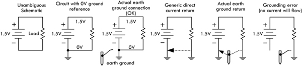
FIGURE 2.33
2.10.2 Different Types of Ground Symbols
To avoid misinterpretations regarding earth grounding, voltage references, and current return paths, less ambiguous symbols have been adopted. Figure 2.34 shows an earth ground (could be Earth or reference), a frame or chassis ground, and a digital and analog reference ground. Unfortunately, the common return for digital and analog is a bit ambiguous, too, but usually a circuit diagram will specify what the symbol is referring to.
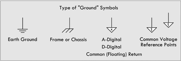
FIGURE 2.34
Table 2.6 provides a rundown on meanings behind these symbols.
TABLE 2.6 Types of Ground Symbols
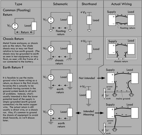
There are a few loose ends on grounding that need mentioning. They are discussed here, with reference to Fig. 2.35.
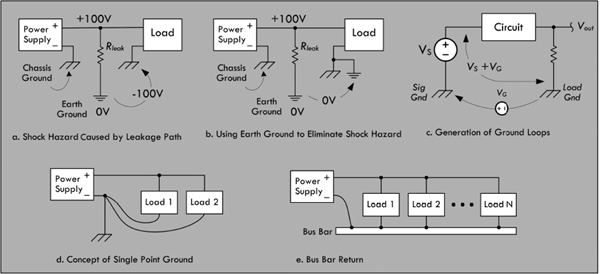
FIGURE 2.35
Shock Hazard
In instances where high voltages are required and chassis grounds or metal frames are used as return paths, shock hazardous conditions can be created if the earth grounds are neglected. For example, in Fig. 2.35a when a load circuit uses a metal enclosure as a chassis ground, resistive leakage paths (unwanted resistive paths) can exist, which result in high voltages between the enclosure and earth ground. If, inadvertently, an earth-grounded object, such as a grounded metal pipe, and the circuit chassis are simultaneously touched, a serious shock will result. To avoid this situation, the chassis is simply wired to an earth ground connection, as shown in Fig. 2.35b. This places the metal pipe and the enclosure at the same potential, eliminating the shock hazard. Similar hazardous conditions can develop in household appliances. Electrical codes require that appliance frames, such as washers and dryers, be connected to earth ground.
Grounding and Noise
The most common cause of noise in large-scale electronic systems is lack of good grounding practices. Grounding is a major issue for practicing design and system engineers. Though it is not within the scope of this book to get into the gory details, we’ll mention some basic practices to avoid grounding problems in your circuits.
If several points are used for ground connections, differences in potential between points caused by inherent impedance in the ground line can cause troublesome ground loops, which will cause errors in voltage readings. This is illustrated in Fig. 2.35c, where two separated chassis grounds are used. VG represents a voltage existing between signal ground and the load ground. If voltage measurements are made between the load ground and the input signal, VS, an erroneous voltage, (VS + VG) is measured. A way to circumvent this problem is to use a single-point ground, as shown in Fig. 2.35d.
The single-point ground concept ensures that no ground loops are created. As the name implies, all circuit grounds are returned to a common point. While this approach looks good on paper, it is usually not practical to implement. Even the simplest circuits can have 10 or more grounds. Connecting all of them to a single point becomes a nightmare. An alternative is to use a ground bus.
A ground bus, or bus bar found in breadboards and prototype boards, or which can be etched in a custom printed circuit board (PCB), serves as an adequate substitute for a single-point ground. A bus bar is simply a heavy copper wire or bar of low resistance that can carry the sum total of all load currents back to the power supply. This bus can be extended along the length of the circuitry so that convenient connections can be made to various components spaced about the board. Figure 2.35e shows a bus bar return. Most prototype boards come with two or three lines of connected terminals extending along the length of the board. One of these continuous strips should be dedicated as a circuit ground bus. All circuit grounds should be tied directly to this bus. Care must be taken to make sure that all lead and wire connections to the bus are secure. For prototype boards, this means a good solder joint; for wire-wrap board, a tight wire wrap; for breadboard, proper gauge wire leads to securely fit within sockets. Bad connections lead to intermittent contact that leads to noise.
Analog and Digital Grounds
Devices that combine analog and digital circuitry should, in general, have their analog and digital grounds kept separate, and eventually connected together at one single point. This is to prevent noise from being generated within the circuits due to a ground current. Digital circuits are notorious for generating spikes of current when signals change state. Analog circuits can generate current spikes when load currents change or during slewing. In either case, the changing currents are impressed across the ground-return impedance, causing voltage variations (use Ohm’s law) at the local ground plane with respect to the system reference ground, often located near the power supply. The ground return impedance consists of resistive, capacitive, and inductive elements, though resistance and inductance are predominant. If a constant current is impressed across the ground return, resistance is primary, and a dc offset voltage will exist. If the current is alternating, resistance, inductance, and capacitance all play a role, and a resulting high-frequency ac voltage will exist. In either case, these voltage variations get injected into the local circuits and are considered noise—capable of screwing up sensitive signal levels used within the local circuits. There are a number of tricks to reduce noise (such as adding capacitors to counterbalance the inductance), but a good trick is to keep the digital and analog ground separated, then attach them together at one single point.
Example: What do the following symbols represent?

FIGURE 2.36
Answer: (a) Probably an analog circuit ground that is terminated at the supply to an actual earth ground connection. (b) A chassis ground that is connected to earth ground, probably to prevent shock hazards. (c) Appears like an analog ground return that is linked to both the chassis and the earth ground. (d) A floating chassis that is connected to circuit return ground—a potential shock hazard. (e) Separate analog and digital grounds that are linked to a common ground point near the supply, which in turn is grounded to earth.
2.11 Electric Circuits
Though we have already shown circuits, let’s define circuits in basic terms. An electric circuit is any arrangement of resistors, wires, or other electrical components (capacitors, inductors, transistors, lamps, motors, etc.) connected together that has some level of current flowing through it. Typically, a circuit consists of a voltage source and a number of components connected together by means of wires or other conductive means. Electric circuits can be categorized as series circuits, parallel circuits, or a combination of series and parallel parts. See Fig. 2.37.
Basic Circuit
A simple lightbulb acts as a load (the part of the circuit on which work must be done to move current through it). Attaching the bulb to the battery’s terminals, as shown, will initiate current flow from the positive terminal to the negative terminal. In the process, the current will power the filament of the bulb, and light will be emitted. (Remember that the term current here refers to conventional current—electrons are actually flowing in the opposite direction.)
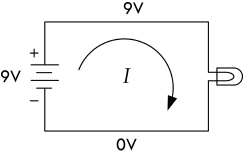
Series Circuit
Connecting load elements (lightbulbs) one after the other forms a series circuit. The current through all loads in series will be the same. In this series circuit, the voltage drops by a third each time current passes through one of the bulbs (all bulbs are exactly the same). With the same battery used in the basic circuit, each light will be one-third as bright as the bulb in the basic circuit. The effective resistance of this combination will be three times that of a single resistive element (one bulb).
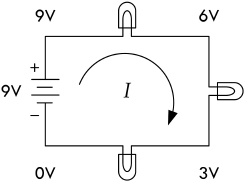
Parallel Circuit
A parallel circuit contains load elements that have their leads attached in such a way that the voltage across each element is the same. If all three bulbs have the same resistance values, current from the battery will be divided equally into each of the three branches. In this arrangement, light-bulbs will not have the dimming effect, as was seen in the series circuit, but three times the amount of current will flow from the battery, hence draining it three times as fast. The effective resistance of this combination will be one-third that of a single resistive element (one bulb).
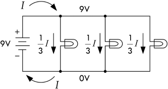
A circuit with load elements placed both in series and in parallel will have the effects of both lowering the voltage and dividing the current. The effective resistance of this combination will be three-halves that of a single resistive element (one bulb).
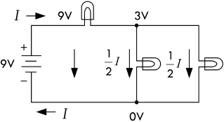
FIGURE 2.37
Circuit Analysis
Following are some important laws, theorems, and techniques used to help predict what the voltage and currents will be within a purely resistive circuit powered by a direct current (dc) source, such as a battery.
2.12 Ohm’s Law and Resistors
Resistors are devices used in circuits to limit current flow or to set voltage levels within circuits. Figure 2.38 shows the schematic symbol for a resistor; two different forms are commonly used. Schematic symbols for variable resistors—resistors that have a manually adjustable resistance, as well as a model of a real-life resistor, are also shown. (The real-life model becomes important later on when we deal with high-frequency ac applications. For now, ignore the model.)
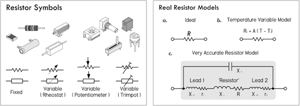
FIGURE 2.38
If a dc voltage is applied across a resistor, the amount of current that will flow through the resistor can be found using Ohm’s law. To find the power dissipated as heat by the resistor, the generalized power (with Ohm’s law substitution) can be used.
V = I × R
(2.15) Ohm’s law
P = IV = V2/R = I2R
(2.16) Ohm’s power law
R is the resistance or the resistor expressed in ohms (Ω), P is the power loss in watts (W), V is the voltage in volts (V), and I is the current in amperes (A).
Resistors typically come with resistance values from 1 Ω to 10,000,000 Ω. Most of the time, the resistance is large enough to adopt a unit prefix convention to simplify the bookkeeping. For example, a 100,000-Ω resistance can be simplified by writing 100 kΩ (or simply 100k, for short). Here k = ×1000. A 2,000,000-Ω resistance can be shortened to 2 MΩ (or 2M, for short). Here M = ×1,000,000.
Conversely, voltages, currents, and power levels are usually small fractions of a unit, in which case it is often easier to use unit prefixes such as m (milli or ×10−3), μ (micro or × 10−6), n (nano or ×10−9), or even p (pico or ×10−12). For example, a current of 0.0000594 A (5.94 × 10⁻⁵ A) can be written in unit prefix form as 59.4 μA. A voltage of 0.0035 (3.5 × 10⁻³ V) can be written in unit prefix form as 3.5 mV. A power of 0.166 W can be written in unit prefix form as 166 mW.
Example: In Fig. 2.39, a 100-Ω resistor is placed across a 12-V battery. How much current flows through the resistor? How much power does the resistor dissipate?
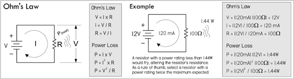
FIGURE 2.39
Answer: See Fig. 2.39.
2.12.1 Resistor Power Ratings
Determining how much power a resistor dissipates is very important when designing circuits. All real resistors have maximum allowable power ratings that must not be exceeded. If you exceed the power rating, you’ll probably end up frying your resistor, destroying the internal structure, and thus altering the resistance. Typical general-purpose resistors come in -, ¼-, ½-, and 1-W power ratings, while high-power resistors can range from 2 to several hundred watts.
So, in the preceding example, where our resistor was dissipating 1.44 W, we should have made sure that our resistor’s power rating exceeded 1.44 W; otherwise, there could be smoke. As a rule of thumb, always select a resistor that has a power rating at least twice the maximum value anticipated. Though a 2-W resistor would work in our example, a 3-W resistor would be safer.
To illustrate how important power ratings are, we examine the circuit shown in Fig. 2.40. The resistance is variable, while the supply voltage is fixed at 5 V. As the resistance increases, the current decreases, and according to the power law, the power decreases, as shown in the graphs. As the resistance decreases, the current and power increase. The far right graph shows that as you decrease the resistance, the power rating of the resistor must increase; otherwise, you’ll burn up the resistor.
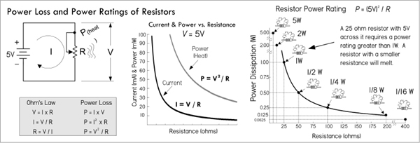
FIGURE 2.40
Example 1: Using an ammeter, you measure a current of 1.0 mA through a 4.7-kΩ resistor. What voltage must exist across the resistor? How much power does the resistor dissipate?
Answer: V = IR = (0.001 A)(4700 Ω) = 4.7 V; P = I2 × R = (0.001 A)2 × (4700 Ω) = 0.0047 W = 4.7 mW
Example 2: Using a voltmeter, you measure 24 V across an unmarked resistor. With an ammeter, you measure a current of 50 mA. Determine the resistance and power dissipated in the resistor.
Answer: R = V/I = (24 V)/(0.05 A) = 480 Ω; P = I × V = (0.05 A) × (24 V) = 1.2 W
Example 3: You apply 3 V to a 1-MΩ resistor. Find the current through the resistor and the power dissipated in the process.
Answer: I = V/R = (3 V)/(1,000,000 Ω) = 0.000003 A = 3 μA; P = V2/R = (3 V)2/(1,000,000 Ω) = 0.000009 W = 9 μW
Example 4: You are given 2-Ω, 100-Ω, 3-kΩ, 68-kΩ, and 1-MΩ resistors, all with 1-W power ratings. What’s the maximum voltage that can be applied across each of them without exceeding their power ratings?
Answer: P = V2/R ⇒ V =  ; voltages must not exceed 1.4 V (2 Ω), 10.0 V (100 Ω), 54.7 V (3 kΩ), 260.7 V (68 kΩ), 1000 V (1 MΩ)
2.12.2 Resistors in Parallel
Rarely do you see circuits that use a single resistor alone. Usually, resistors are found connected in a variety of ways. The two fundamental ways of connecting resistors are in series and in parallel.
When two or more resistors are placed in parallel, the voltage across each resistor is the same, but the current through each resistor will vary with resistance. Also, the total resistance of the combination will be lower than that of the lowest resistance value present. The formula for finding the total resistance of resistors in parallel is:
(2.17)
(2.18) Two resistors in parallel
The dots in the equation indicate that any number of resistors can be combined. For only two resistances in parallel (a very common case), the formula reduces to Eq. 2.18.
(You can derive the resistor-in-parallel formula by noting that the sum of the individual branch currents is equal to the total current: Itotal = I1 + I2 + I3 + … IN. This is referred to as Kirchhoff’s current law. Then, applying Ohm’s law, we get: Itotal = V1/R1 + V2/R2 + V3/R3 + … VN/RN. Because all resistor voltages are equal to Vtotal since they share the same voltage across them, we get: Itotal = Vtotal/R1 + Vtotal/R2 + Vtotal/R3 + … Vtotal/RN. Factoring out Vtotal, we get: Itotal = Vtotal (1/R1 + 1/R2 + 1/R3 … 1/R4). We call the term in brackets Rtotal.
Note that there is a shorthand for saying that two resistors are in parallel. The shorthand is to use double bars | | to indicate resistors in parallel. So to say R1 is in parallel with R2, you would write R1 | | R2. Thus, you can express two resistors in parallel in the following ways:
In terms of arithmetic order of operation, the | | can be treated similar to multiplication or division. For example, in the equation Zin = R1 + R2 | | Rload, you calculate R2 and Rload in parallel first, and then you add R1.
Example 1: If a 1000-Ω resistor is connected in parallel with a 3000-Ω resistor, what is the total or equivalent resistance? Also calculate total current and individual currents, as well as the total and individual dissipated powers.
To find how much current flows through each resistor, apply Ohm’s law:
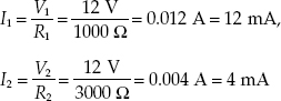
These individual currents add up to the total input current:
This statement is referred to as Kirchhoff’s current law. With this law, and Ohm’s law, you come up with the current divider equations, shown at the bottom of Fig. 2.41. These equations come in handy when you know the input current but not the input voltage.
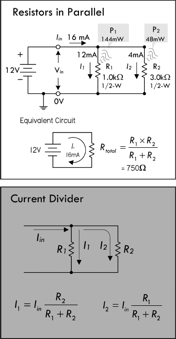
FIGURE 2.41
We could have just as easily found the total current using:
Iin = Vin/Rtotal = (12 V)/(750 Ω) = 0.016 A = 16 mA
To find how much power resistors in parallel dissipate, apply the power law:
Ptot = IinVin = (0.0016 A)(12 V) = 0.192 W = 192 mW
P1 = I1Vin = (0.012 A)(12 V) = 0.144 W = 144 mW
P2 = I2Vin = (0.004 A)(12 V) = 0.048 W = 48 mW
Example 2: Three resistors R1 = 1 kΩ, R2 = 2 kΩ, R3 = 4 kΩ are in parallel. Find the equivalent resistance. Also, if a 24-V battery is attached to the parallel circuit to complete a circuit, find the total current, individual currents through each of the resistors, total power loss, and individual resistor power losses.
The total resistance for resistors in parallel:
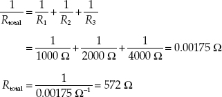
I1 = V1/R1 = 24 V/1000 Ω = 0.024 A = 24 mA
I2 = V2/R2 = 24 V/2000 Ω = 0.012 A = 12 mA
I3 = V3/R3 = 24 V/4000 Ω = 0.006 A = 6 mA
The total current, according to Kirchhoff’s current law:
Itotal = I1 + I2 + I3 = 24 mA + 12 mA + 6 mA = 42 mA
The total power dissipated by the parallel resistors:
Ptotal = Itotal × Vtotal = 0.042 A × 24 V = 1.0 W
The power dissipated by individual resistors is shown in Fig. 2.42.
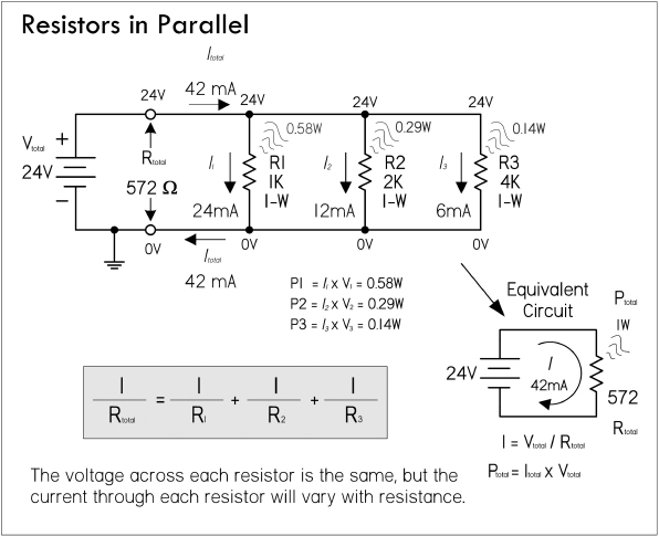
FIGURE 2.42
2.12.3 Resistors in Series
When a circuit has a number of resistors connected in series, the total resistance of the circuit is the sum of the individual resistances. Also, the amount of current flowing through each resistor in series is the same, while the voltage across each resistor varies with resistance. The formula for finding the total resistance of resistors in series is:
(2.19)
The dots indicate that as many resistors as necessary may be added.
You can derive this formula by noting that the sum of all the voltage drops across each series resistor will equal the applied voltage across the combination Vtotal = V1 + V2 + V3 + … + VN. This is referred to as Kirchhoff’s voltage law. Applying Ohm’s law, and noting that the same current I flows through each resistor, we get: IRtotal = IR1 + IR2 + IR3 + … + IRN. Canceling the I’s you get: Rtotal = R1 + R2 + R3 + R4 + …)
Example 1: If a 1.0-kΩ resistor is placed in series with a 2.0-kΩ resistor, the total resistance becomes:
Rtot = R1 + R2 = 1000 Ω + 2000 Ω = 3000 Ω = 3 kΩ
When these series resistors are placed in series with a battery, as shown in Fig. 2.43, the total current flow I is simply equal to the applied voltage Vin, divided by the total resistance:
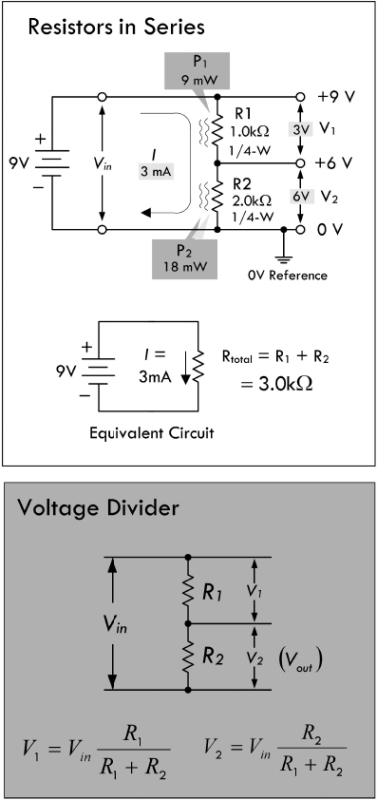
FIGURE 2.43
Since the circuit is a series circuit, the currents through each resistor are equal to the total current I:
I1 = 3 mA, I2 = 3 mA
To find the voltage drop across each resistor, apply Ohm’s law:
V1 = I1 × R1 = 0.003 A × 1000 Ω = 3 V
V2 = I2 × R2 = 0.003 A × 2000 Ω = 6 V
Now, we didn’t really have to calculate the current. We could have just plugged I = Vin/Rtot into I1 and I2 in the preceding equations and got:
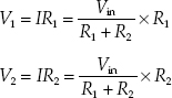
(Voltage divider equations)
These equations are called voltage divider equations and are so useful in electronics that it is worth memorizing them. (See Fig. 2.43.) Often V2 is called the output voltage Vout.
The voltage drop across each resistor is directly proportional to the resistance. The voltage drop across the 2000-Ω resistor is twice as large as that of 1000-Ω resistor. Adding both voltage drops together gives you the applied voltage of 9 V:
Vin = V1 + V2 9 V = 3 V + 6 V
The total power loss and individual resistor power losses are:
Ptot = IVin = (0.003 A)(9 V) = 0.027 W = 27 mW
(Ptot = I2Rtot = (0.003 A)2(3000 Ω) = 0.027 W = 27 mW)
P1 = I2R1 = (0.003 A)2(1000 Ω) = 0.009 W = 9 mW
P2 = I2R2 = (0.003 A)2(2000 Ω) = 0.018 W = 18 mW
The larger resistor dissipates twice as much power.
Example 2: The input of an IC requires a constant 5 V, but the supply voltage is 9 V. Use the voltage divider equations to create a voltage divider with an output of 5 V. Assume the IC has such a high input resistance (10 MΩ) that it practically draws no current from the divider.
Answer: Since we assume the IC draws no current, we can apply the voltage divider directly:
We must choose voltage divider resistors, making sure our choice doesn’t draw too much current, causing unnecessary power loss. To keep things simple for now, let’s choose R2 to be 10 kΩ. Rearranging the voltage divider and solving for R1:
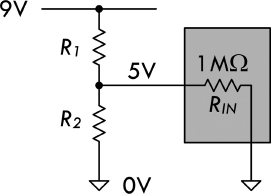
FIGURE 2.44
Example 3: You have a 10-V supply, but a device that is to be connected to the supply is rated at 3 V and draws 9.1 mA. Create a voltage divider for the load device.
Answer: In this case, the load draws current and can be considered a resistor in parallel with R2. Therefore, using the voltage divider relation without taking the load into consideration will not work. We must apply what is called the 10 percent rule.
The 10 Percent Rule: This rule is a standard method for selecting R1 and R2 that takes into account the load and minimizes unnecessary power losses in the divider.
The first thing you do is select R2 so that I2 is 10 percent of the desired load current. This resistance and current are called the bleeder resistance and bleeder current. The bleeder current in our example is:
Ibleed = I2 = (0.10)(9.1 mA) = 0.91 mA
Using Ohm’s law, next we calculate the bleeder resistance:
Rbleed = R2 = 3 V/0.00091 A = 3297 Ω
Considering resistor tolerances and standard resistance values, we select a resistor in close vicinity—3300 Ω.
Next, we need to select R1, so that the output is maintained at 3 V.
To do this, simply calculate the total current through the resistor and use Ohm’s law:
I1 = I2 + Iload = 0.91 mA + 9.1 mA = 10.0 mA = 0.01 A
In terms of power ratings:
P1 = V12/R1 = (7 V)2/(700 Ω) = 0.07 W = 70 mW
PR2 = V22/R2 = (3 V)2/(3300 Ω) = 0.003 W = 3 mW
Low-power ¼-W resistors will suffice.
In actual practice, the computed value of the bleeder resistor does not always come out to an even value. Since the rule of thumb for bleeder current is only an estimated value, the bleeder resistor can be of a value close to the computed value. (If the computed value of the resistance were a 500 Ω, 510 Ω resistor could be used.) Once the actual value of the bleeder resistor is selected, the bleeder current must be recomputed. The voltage developed by the bleeder resistor must be equal to the voltage requirement of the load in parallel with the bleeder resistor. We’ll discuss voltage dividers, as well as more complex divider arrangements, in the section on resistors in Chap. 3.
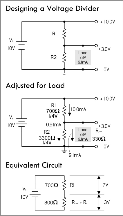
FIGURE 2.45
Example: Find the equivalent resistance of series resistors R1 = 3.3k, R2 = 4.7k, R3 = 10k. If a 24-V battery is attached to the series resistors to complete a circuit, find the total current flow, the individual voltage drops across the resistors, the total power loss, and the individual power loss of each resistor.
The equivalent resistance of the three resistors:
The total current flow through the resistors is:
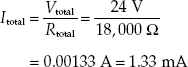
Using Ohm’s law, the voltage drops across the resistors are:
V1 = Itotal × R1 = 1.33 mA × 3.3 kΩ = 4.39 V
V2 = Itotal × R2 = 1.33 mA × 4.7 kΩ = 6.25 V
V3 = Itotal × R3 = 1.33 mA × 10 kΩ = 13.30 V
The total power dissipated is:
Ptotal = Itotal × Vtotal = 1.33 mA × 24 V = 32 mW
Power dissipated by individual resistors is shown in Fig. 2.46.
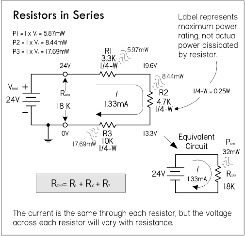
FIGURE 2.46
2.12.4 Reducing a Complex Resistor Network
To find the equivalent resistance for a complex network of resistors, the network is broken down into series and parallel combinations. A single equivalent resistance for these combinations is then found, and a new and simpler network is formed. This new network is then broken down and simplified. The process continues over and over again until a single equivalent resistance is found. Here’s an example of how reduction works.
Example 1: Find the equivalent resistance of the network attached to the battery by using circuit reduction. Afterward, find the total current flow supplied by the battery to the network, the voltage drops across all resistors, and the individual current through each resistor.
R2 and R3 form a parallel branch that can be reduced to:
This equivalent resistance and R1 are in series, so their combined resistance is:
Req(2) = R1 + Req(1) = 5.0 kΩ + 4.4 kΩ = 9.4 kΩ
The total current flow through the circuit and through R1 is:
The voltage across R2 and R3 is the same as that across Req(1):
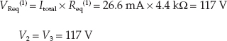
The current through R2 and R3 are found using Ohm’s law:
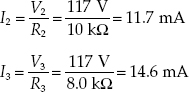
The voltage across R1 is, by Kirchhoff’s voltage law:
V1 = 250 V – 117 V = 133 V
Alternatively we could have used Ohm’s law:
V1 = I1 × R1 = (26.6 mA)(5.0 kΩ) = 133 V
Example 2: Find the equivalent resistance of the following network, along with the total current flow, the individual current flows, and individual voltage drops across the resistors.
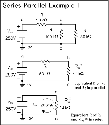
FIGURE 2.47
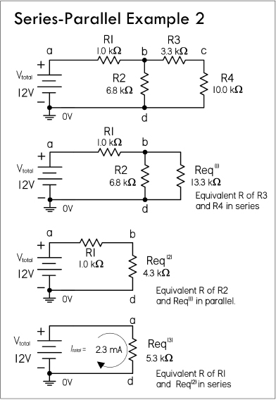
FIGURE 2.48
This equivalent resistance is in parallel with R2:
This new equivalent resistance is in series with R1:
The total current flow is:
The voltage across Req(2) or point voltage at b is:
The voltage across R1 is:
You can confirm this using Kirchhoff’s voltage law:
12 V – 9.7 V = 2.3 V
The current through R2:
The current through Req(1), also through R3 and R4:
You can confirm this using Kirchhoff’s current law:
2.26 mA – 1.43 mA = 0.73 mA.
The voltage across R3:
The voltage across R4:
You can confirm this using Kirchhoff’s voltage law:
9.7 V − 2.4 V = 7.3 V
Example 1: You wish to create a multiple voltage divider that powers three loads: load 1 (75 V, 30 mA), load 2 (50 V, 10 mA), and load 3 (25 V, 10 mA). Use the 10 percent rule and Fig. 2.49 to construct the voltage divider.
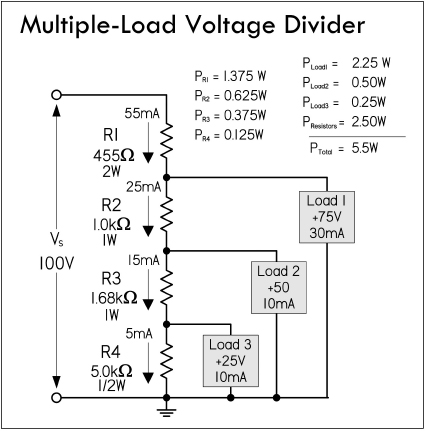
FIGURE 2.49
An important point in determining the resistor when applying the 10 percent rule of thumb is that to calculate the bleeder current, you must take 10 percent of the total load current. The steps are as follows:
Find the bleeder current, which is 10 percent (0.1) of the total current:
IR4 = 0.1 × (10 mA + 10 mA + 30 mA) = 5 mA
To find R4 (bleeder resistor), use Ohm’s law:
R4 = (25 V − 0 V)/(0.005 A) = 5000 Ω
The current through R3 is equal to the current through R4 plus the current through load 3:
IR3 = IR4 + Iload3 = 5 mA + 10 mA = 15 mA
To find R3, use Ohm’s law, using the voltage difference between load 2 and load 3: R3 = (50 V − 25 V)/(0.015 A) = 1667 Ω or 1.68 kΩ, considering tolerances and standard resistance values.
The current through R2 is:
IR2 = IR3 + Iload2 = 15 mA + 10 mA = 25 mA
Using Ohm’s law, R2 = (75 V − 50 V)/(0.025 A) = 1000 Ω
The current through R1 is:
IR1 = IR2 + Iload1 = 25 mA + 30 mA = 55 mA
Using Ohm’s law: R1 = (100 V − 75 V)/(0.055 A) = 455 Ω
To determine resistor power ratings and total power losses in loads use P = IV. See results in Fig. 2.49.
Example 2: In many cases, the load for a voltage divider requires both positive and negative voltages. Positive and negative voltages can be supplied from a single-source voltage by connecting the ground return between two of the divider resistors. The exact point in the circuit at which the ground is placed depends upon the voltages required by the loads.
For example, the voltage divider in Fig. 2.50 is designed to provide the voltage and current to three loads from a given source voltage:
Load 1: +50 V @ 50 mA
Load 2: +25 V @ 10 mA
Load 3: −25 V @ 100 mA
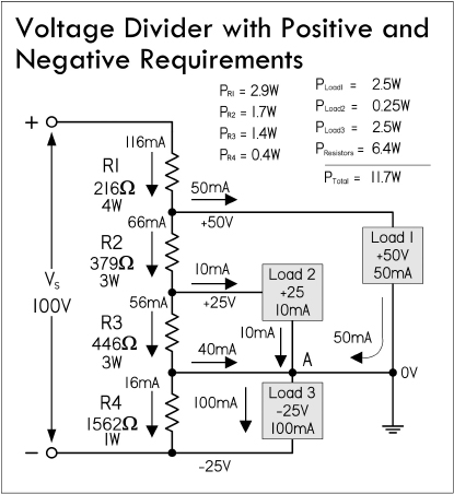
FIGURE 2.50
The values of R4, R2, and R1 are computed exactly as was done in the preceding example. IR4 is the bleeder current and can be calculated as follows:
IR4 = 10% × (Iload1 + Iload2 + Iload3) = 16 mA
Calculating R1:
R4 = 25 V/0.016 A = 1562 Ω
To calculate current through R2, use Kirchhoff’s current law (at point A):
IR3 + Iload2 + Iload1 + IR4 + Iload3 = 0
IR3 + 10 mA + 50 mA − 16 mA − 100 mA = 0
IR3 = 56 mA
Calculating R3: R3 = 25 V/(0.056 A) = 446 Ω.
Calculating IR2: IR2 = IR3 + Iload2 = 56 mA + 10 mA = 66 mA.
Then R2 = 25 V/(0.066 A) = 379 Ω.
Calculating IR1 = IR2 + Iload1 = 66 mA + 50 mA = 116 mA.
Then R1 = 25 V/0.116 A = 216 Ω.
Though voltage dividers are simple to apply, they are not regulated in any way. If a load’s resistance changes, or if there is variation in the supply voltage, all loads will experience a change in voltage. Therefore, voltage dividers should not be applied to circuits where the divider will be weighed down by changes in load. For applications that require steady voltage and that draw considerable current, it is best to use an active device, such as a voltage regulator IC—more on this later.
2.13 Voltage and Current Sources
An ideal voltage source is a two-terminal device that maintains a fixed voltage across its terminals. If a variable load is connected to an ideal voltage source, the source will maintain its terminal voltage regardless of changes in the load resistance. This means that an ideal voltage source will supply as much current as needed to the load in order to keep the terminal voltage fixed (in I = V/R, I changes with R, but V is fixed). Now a fishy thing with an ideal voltage source is that if the resistance goes to zero, the current must go to infinity. Well, in the real world, there is no device that can supply an infinite amount of current. If you placed a real wire between the terminals of an ideal voltage source, the calculated current would be so large it would melt the wire. To avoid this theoretical dilemma, we must define a real voltage source (a battery, plug-in dc power supply, etc.) that can supply only a maximum finite amount of current. A real voltage source resembles an ideal voltage source with a small series internal resistance or source resistance rs, which is a result of the imperfect conducting nature of the source (resistance in battery electrolyte and lead, etc.). This internal resistance tends to reduce the terminal voltage, the magnitude of which depends on its value and the amount of current that is drawn from the source (or the size of the load resistance).
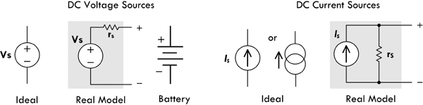
FIGURE 2.51
In Fig. 2.52, when an ideal voltage source is open-circuited (no load connected between its terminals), the terminal voltage (VT) equals the ideal source voltage (VS)—there is no voltage drop across the resistor, since current can’t pass through it due to an incomplete circuit condition.
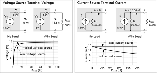
FIGURE 2.52
However, when a load Rload is attached across the source terminals, Rload and rs are connected in series. The voltage at the terminal can be determined by using the voltage divider relation:
From the equation, you can see that when Rload is very large compared to rs, (1000 times greater or more), the effect of rs is so small that it may be ignored. However, when Rload is small or closer to rs in size, you must take rs into account when doing your calculations and designing circuits. See the graph in Fig. 2.52.
In general, the source resistance for dc power supplies is usually small; however, it can be as high as 600 Ω in some cases. For this reason, it’s important to always adjust the power supply voltage with the load connected. In addition, it is a good idea to recheck the power supply voltage as you add or remove components to or from a circuit.
Another symbol used in electronics pertains to dc current sources—see Fig. 2.52. An ideal current source provides the same amount of source current IS at all times to a load, regardless of load resistance changes. This means that the terminal voltage will change as much as needed as the load resistance changes in order to keep the source current constant.
In the real world, current sources have a large internal shunt (parallel) resistance rs, as shown in Fig. 2.52. This internal resistance, which is usually very large, tends to reduce the terminal current IT, the magnitude of which depends on its value and the amount of current that is drawn from the source (or the size of load resistance).
When the source terminals are open-circuited, IT must obviously be zero. However, when we connect a load resistance Rload across the source terminals, Rload and rs form a parallel resistor circuit. Using the current divider expression, the terminal current becomes:
From this equation, you can see that when Rload is small compared to rs, the dip in current becomes so small it usually can be ignored. However, when Rload is large or closer to rs in size, you must take rs into account when doing your calculations.
A source may be represented either as a current source or a voltage source. In essence, they are duals of each other. To translate between the voltage source and current source representation, the resistance value is kept the same, while the voltage of the source is translated into the current of the source using Ohm’s law. See Fig. 2.53 for details.
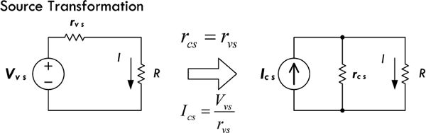
FIGURE 2.53
One way to look at an ideal current source is to say it has an internal resistance that is infinite, which enables it to support any kind of externally imposed potential difference across its terminals (e.g., a load’s resistance changes). An approximation to an ideal current source is a voltage source of very high voltage V in series with a very large resistance R. This approximation would supply a current V/R into any load that has a resistance much smaller than R. For example, the simple resistive current source circuit shown in Fig. 2.54 uses a 1-kV voltage source in series with a 1-MΩ resistor. It will maintain the set current of 1 mA to an accuracy within 1 percent over a 0-to 10-V range (0 < Rload < 10 kΩ). The current is practically constant even though the load resistance varies, since the source resistance is much greater than the load resistance, and thus the current remains practically constant. (I = 1000 V/(1,000,000 Ω + 10,0000 Ω. Since 1,000,000 Ω is so big, it overshadows Rload.)
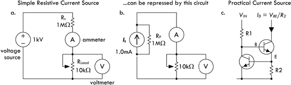
FIGURE 2.54
A practical current source is usually an active circuit made with transistors, as shown in Fig. 2.54c. Vin drives current through R1 into the base of the second transistor, so current flows into the transistor’s collector, through it, and out its emitter. This current must flow through R2. If the current gets too high, the first transistor turns on and robs the second transistor of base current, so its collector current can never exceed the value shown. This is an excellent way of either making a current source or limiting the available current to a defined maximum value.
2.14 Measuring Voltage, Current, and Resistance
Voltmeters, ammeters, and ohmmeters, used to measure voltage, current, and resistance, ideally should never introduce any effects within the circuit under test. In theory, an ideal voltmeter should draw no current as it measures a voltage between two points in a circuit; it has infinite input resistance Rin. Likewise, an ideal ammeter should introduce no voltage drop when it is placed in series within the circuit; it has zero input resistance. An ideal ohmmeter should provide no additional resistance when making a resistance measurement.
Real meters, on the other hand, have limitations that prevent them from making truly accurate measurements. This stems from the fact that the circuit of a meter requires a sample current from the circuit under test in order to make a display measurement. Figure 2.55 shows symbols for an ideal voltmeter, ammeter, and ohmmeter, along with the more accurate real-life equivalent circuits.
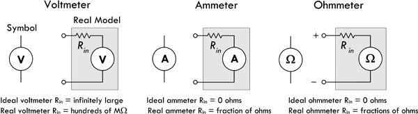
FIGURE 2.55
An ideal voltmeter has infinite input resistance and draws no current; a real voltmeter’s input resistance is several hundred MΩs. An ideal ammeter has zero input resistance and provides no voltage drop; a real ammeter’s input resistance is fractions of ohms. An ideal ohmmeter has zero internal resistance; a real ohmmeter’s internal resistance is fractions of ohms. It is important to read your instrument manuals to determine the internal resistances.
The effects of meter internal resistance are shown in Fig. 2.56. In each case, the internal resistance becomes part of the circuit. The percentages of error in measurements due to the internal resistances become more pronounced when the circuit resistances approach the meters’ internal resistance.
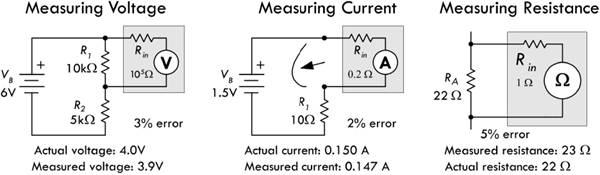
FIGURE 2.56
Figure 2.57 shows the actual makeup of a basic analog multimeter. Note that this device is overly simplistic; real meters are much more sophisticated, with provisions for range selection, ac measurements, and so on. At any rate, it shows you that the meters are nonideal due to the sample current required to drive the galvanometer’s needle.
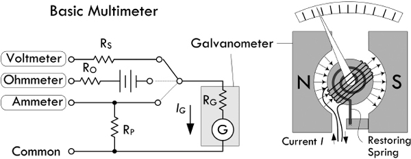
FIGURE 2.57 The heart of this simple analog multimeter is a galvanometer which measures current flow IG. Current sent through the galvanometer’s wire leads will generate a magnetic field from the coil windings in the center rotor. Since the coil is tilted relative to the N-S alignment of the permanent magnet, the rotor will rotate in accordance with the amount of current flow. Normally you get full deflection of the needle at extremely low current levels, so you can add a parallel resistor to divert current flow away from the galvanometer. The galvanometer can also be used as a voltmeter by placing its lead at the point voltages within the circuit. If there is a voltage difference at the leads, a current will flow into the galvanometer and move the needle in proportion to the voltage magnitude. A series resistor is used to limit current flow and needle deflection. A galvanometer can be used to make an ohmmeter, too, provided you place a battery in series with it. Again, to calibrate needle deflection, a series resistor RO is used.
2.15 Combining Batteries
The two battery networks in Fig. 2.58 show how to increase the supply voltage and/or increase the supply current capacity. To increase the supply voltage, batteries are placed end to end or in series; the terminal voltages of each battery add together to give a final supply voltage equal to the sum from the batteries. To create a supply with added current capacity (increased operating time), batteries can be placed in parallel—positive terminals are joined together, as are negative terminals, as shown in Fig. 2.58. The power delivered to the load can be found using Ohm’s power law: P = V2/R, where V is the final supply voltage generated by all batteries within the network. Note that the ground symbol shown here acts simply as a 0-V reference, not as an actual physical connection to ground. Rarely would you ever connect a physical ground to a battery-operated device.
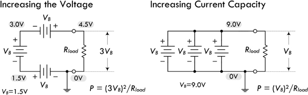
FIGURE 2.58
Note: When placing batteries in parallel, it’s important that the voltages and chemistry be the same—choose all similar batteries, all fresh. If the voltages are different, you can run into problems.
The most common problems (faults) in circuits are open circuits and shorts. A short circuit in all or part of a circuit causes excessive current flow. This may blow a fuse or burn out a component, which may result in an open-circuit condition. An open circuit represents a break in the circuit, preventing current from flowing. Short circuits may be caused by a number of things—from wire crossing, insulation failure, or solder splatter inadvertently linking two separate conductors within a circuit board. An open circuit may result from wire or component lead separation from the circuit, or from a component that has simply burned out, resulting in a huge resistance. Figure 2.59 shows cases of open-and short-circuit conditions. A fuse, symbolized  , is used in the circuit and will blow when the current through it exceeds its current rating, given in amps.
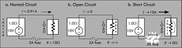
FIGURE 2.59
A weird thing about a short circuit, if you consider all components to be ideal in nature, is that an infinite current will flow if an ideal voltage source is short-circuited, while the voltage across the short goes to zero. Real voltage sources have internal resistance, as do the conductors, so the maximum current level is reduced. However, there is usually still plenty of current available to do damage.
You can often diagnose a short circuit by noting a burning smell, or by placing your hand nearby to sense any components overheating. To prevent short circuits from destroying circuits, various protection devices can be used, such as fuses, transient voltage suppressors, and circuit breakers. These devices sense when too much current is flowing, and they will blow or trip, thus creating an open-circuit condition to limit excessive current damage.
Example 1: In the series circuit in Fig. 2.60, determine how much current flows through the normal circuit (a), then determine how much current flows when there is a partial short (b), and determine how much current would flow during a full short if the 1-A fuse weren’t in place. Assume an internal 3-Ω circuit resistance at the moment of a full-short condition.
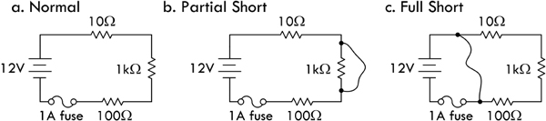
FIGURE 2.60
Answer: a. 11 mA, b. 109 mA, c. 4 A—fuse blows.
Example 2: In the parallel circuit in Fig. 2.61, determine the total current flow in the normal circuit (a), the open circuit (b), and the current flow in the short circuit (c). Assume the internal resistance of the battery is 0.2 Ω below 3 A, but goes to 2 Ω during a short-circuit condition.
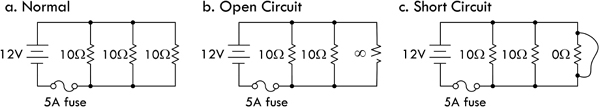
FIGURE 2.61
Answer: a. 3.4 A, b. 2.3 A, c. 6 A—fuse blows.
Example 3: In the parallel circuit in Fig. 2.62, loads B, C, and D receive no power when S2 is closed (assume all other switches are already closed); however, load A receives power. You notice the fuse is blown. After replacing the fuse, you close S2 with S3 and S4 open, and the fuse doesn’t blow. Closing S3 power on loads B and C has no effect. Closing S4 causes B and C to turn off—load D receives no power, either. The fuse is blown again. What is the problem?
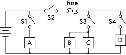
FIGURE 2.62
Answer: Load D has a short in it.
2.17 Kirchhoff’s Laws
Often, you will run across a circuit that cannot be analyzed with simple resistor circuit reduction techniques alone. Even if you could find the equivalent resistance by using circuit reduction, it might not be possible for you to find the individual currents and voltage through and across the components within the network. Likewise, if there are multiple sources, or complex networks of resistors, using Ohm’s law, as well as the current and voltage divider equations, may not cut it. For this reason, we turn to Kirchhoff’s laws.
Kirchhoff’s laws provide the most general method for analyzing circuits. These laws work for either linear (resistor, capacitors, and inductors) or nonlinear elements (diodes, transistors, etc.), no matter how complex the circuit gets. Kirchhoff’s two laws are stated as follows.
Kirchhoff’s Voltage Law (or Loop Rule): The algebraic sum of the voltages around any loop of a circuit is zero:
(2.20)
In essence, Kirchhoff’s voltage law is a statement about the conservation of energy. If an electric charge starts anywhere in a circuit and is made to go through any loop in a circuit and back to its starting point, the net change in its potential is zero.
To show how Kirchhoff’s voltage law works, we consider the circuit in Fig. 2.63. We start anywhere we like along the circuit path—say, at the negative terminal of the 5-V battery. Then we start making a loop trace, which in this case we choose to go clockwise, though it doesn’t really matter which direction you choose. Each time we encounter a circuit element, we add it to what we’ll call our ongoing loop equation. To determine the sign of the voltage difference, we apply the loop trace rules shown in the shaded section of the figure. We continue adding elements until we make it back to the start of the loop, at which point we terminate the loop equation with an “= 0.”
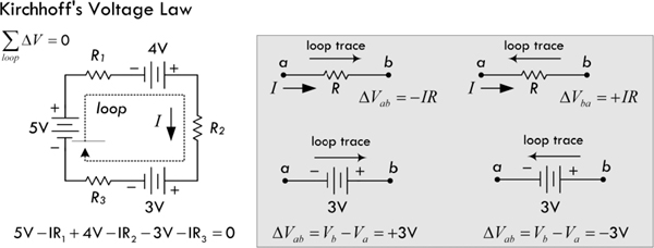
FIGURE 2.63
As noted, Kirchhoff’s voltage law applies to any circuit elements, both linear and nonlinear. For example, the rather fictitious circuit shown here illustrates Kirchhoff’s voltage law being applied to a circuit that has other elements besides resistors and dc sources—namely, a capacitor, an inductor, and a nonlinear diode, along with a sinusoidal voltage source. We can apply the loop trick, as we did in the preceding example, and come up with an equation. As you can see, the expressions used to describe the voltage changes across the capacitor, inductor, and diode are rather complex, not to mention the solution to the resulting differential equation. You don’t do electronics this way (there are tricks), but it nevertheless demonstrates the universality of Kirchhoff’s law.
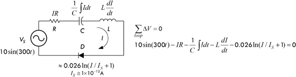
FIGURE 2.64
Kirchhoff’s Current Law (or Junction Rule): The sum of the currents that enter a junction equals the sum of the currents that leave the junction:
(2.21)
Kirchhoff’s current law is a statement about the conservation of charge flow through a circuit: at no time are charges created or destroyed.
The following example shows both Kirchhoff’s current and voltage laws in action.
Example: By applying Kirchhoff’s laws to the following circuit, find all the unknown currents, I1, I2, I3, I4, I5, I6, assuming that R1, R2, R3, R4, R5, R6, and V0 are known. After that, the voltage drops across the resistors V1, V2, V3, V4, V5, and V6 can be found using Ohm’s law: Vn = InRn.
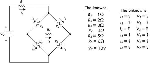
FIGURE 2.65
Answer: To solve this problem, you apply Kirchhoff’s voltage law to enough closed loops and apply Kirchhoff’s current law to enough junctions that you end up with enough equations to counterbalance the unknowns. After that, it is simply a matter of doing some algebra. Figure 2.66 illustrates how to apply the laws in order to set up the final equations.
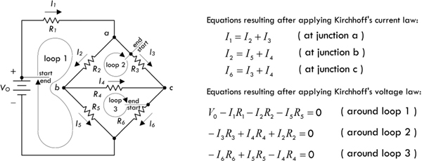
FIGURE 2.66
In Fig. 2.66, there are six equations and six unknowns. According to the rules of algebra, as long as you have an equal number of equations and unknowns, you can usually figure out what the unknowns will be. There are three ways I can think of to solve for the unknowns in this case. First, you could apply the old “plug and chug” method, better known as the substitution method, where you combine all the equations together and try to find a single unknown, and then substitute it back into another equation, and so forth. A second method, which is a lot cleaner and perhaps easier, involves using matrices. A book on linear algebra will tell you all you need to know about using matrices to solve for the unknown.
A third method that I think is useful—practically speaking—involves using a trick with determinants and Cramer’s rule. The neat thing about this trick is that you do not have to know any math—that is, if you have a mathematical computer program or calculator that can do determinants. The only requirement is that you be able to plug numbers into a grid (determinant) and press “equals.” I do not want to spend too much time on this technique, so I will simply provide you with the equations and use the equations to find one of the solutions to the resistor circuit problem. See Fig. 2.67a.
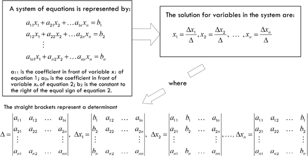
FIGURE 2.67a
For example, you can find Δ for the system of equations from the resistor problem by plugging all the coefficients into the determinant and pressing the “evaluate” button on the calculator or computer. See Fig. 2.67b.
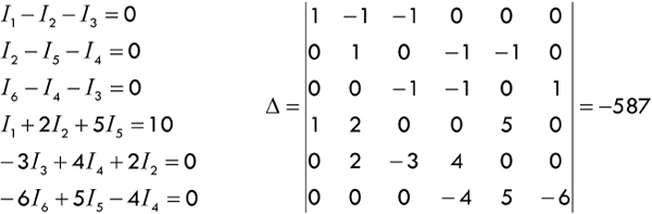
FIGURE 2.67b
Now, to find, say, the current through R5 and the voltage across it, you find ΔI5, then use I5 = ΔI5/Δ to find the current. Then you use Ohm’s law to find the voltage. Figure 2.67c shows how it is done.
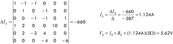
FIGURE 2.67c
To solve for the other currents (and voltages), simply find the other ΔI’s and divide by Δ.
The last approach, as you can see, requires a huge mathematical effort to get a single current value. For simplicity, you can find out everything that’s going on in the circuit by running it through a circuit simulator program. For example, using MultiSim, we get the results in Fig. 2.68:
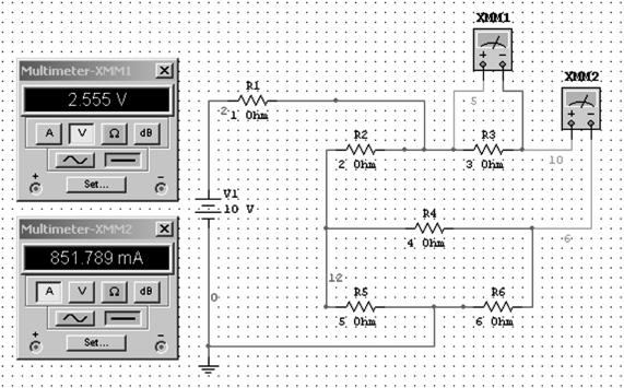
Doing long calculations is good theoretical exercise, but in practice it’s a waste of time. A problem such as this only takes a few minutes to solve using a simulator. The results from simulation:
V1 = 2.027 V I1 = 2.027 A
V2 = 2.351 V I2 = 1.175 A
V3 = 2.555 V I3 = 0.852 A
V4 = 0.204 V I4 = 0.051 A
V5 = 5.622 V I5 = 1.124 A
V6 = 5.417 V I6 = 0.903 A
FIGURE 2.68
Plugging the results back into the diagram, you can see Kirchhoff’s voltage and current laws in action, as shown in Fig. 2.69. Take any loop, sum the changes in voltage across components, and you get 0 (note that the voltages indicated in black shadow represent point voltages relative to 0-V reference ground). Also, the current that enters any junction will equal the sum of the currents exiting the junction, and vice versa—Kirchhoff’s current law.
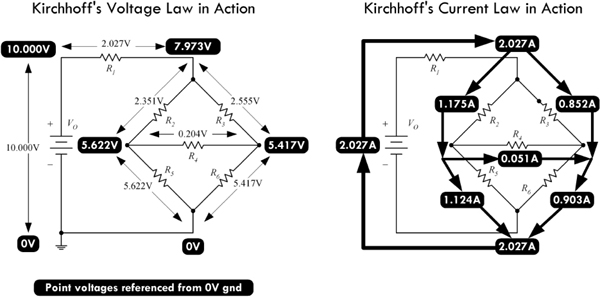
FIGURE 2.69
Now, before you get too gung ho about playing with equations or become lazy by grabbing a simulator, you should check out a special theorem known as Thevenin’s theorem. This theorem uses some very interesting tricks to analyze circuits, and it may help you avoid dealing with systems of equations or having to resort to simulation. Thevenin’s theorem utilizes something called the superposition theorem, which we must consider first.
2.18 Superposition Theorem
The superposition theorem is an important concept in electronics that is useful whenever a linear circuit contains more than one source. It can be stated as follows:
Superposition theorem: The current in a branch of a linear circuit is equal to the sum of the currents produced by each source, with the other sources set equal to zero.
The proof of the superposition theorem follows directly from the fact that Kirchhoff’s laws applied to linear circuits always result in a set of linear equations, which can be reduced to a single linear equation in a single unknown. This means that an unknown branch current can thus be written as a linear superposition of each of the source terms with an appropriate coefficient. Be aware that the superposition should not be applied to nonlinear circuits.
It is important to make clear what it means to set sources equal to zero when interrupting the superposition theorem. A source may be a voltage source or a current source. If the source is a voltage source, to set it to zero means that the points in the circuit where its terminals were connected must be kept at the same potential. The only way to do this is to replace the voltage source with a conductor, thus creating a short circuit. If the source is a current source, to set it to zero means to simply remove it and leave the terminals open, thus creating an open circuit. A short circuit causes the voltage to be zero; an open circuit causes the current to be zero.
In Fig. 2.70, we will analyze the circuit using the superposition theorem. The circuit contains two resistors, a voltage source, and a current source.
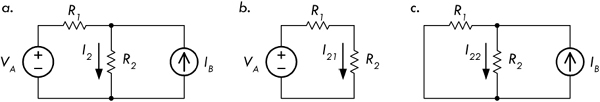
FIGURE 2.70 The circuit in (a) can be analyzed using the superposition theorem by considering the simpler circuits in (b) and (c).
First we remove the current source (create an open circuit at its terminals), as shown in Fig. 2.70b. The new current through R2 due to the voltage source alone is just VA divided by the equivalent resistance:
This current is called the partial current in branch 2 due to source 1. Next, the voltage source is removed and set to zero by replacing it with a conductor (we short it); see Fig. 2.70c. The resulting circuit is a current divider, and the resulting partial current is given by:
Applying the superposition, we add the partial current to get the total current:
The current through R1 could have been determined in a similar manner, with the following result:
The superposition theorem is an important tool whose theory makes possible complex impedance analysis in linear, sinusoidally driven circuits—a subject we will cover a bit later. The superposition is also an underlying mechanism that makes possible two important circuit theorems: Thevenin’s theorem and Norton’s theorem. These two theorems, which use some fairly ingenious tricks, are much more practical to use than the superposition. Though you will seldom use the superposition directly, it is important to know that it is the base upon which many other circuit analysis tools rest.
2.19.1 Thevenin’s Theorem
Say that you are given a complex circuit such as that shown in Fig. 2.71. Pretend that you are only interested in figuring out what the voltage will be across terminals A and F (or any other set of terminals, for that matter) and what amount of current will flow through a load resistor attached between these terminals. If you were to apply Kirchhoff’s laws to this problem, you would be in trouble—the amount of work required to set up the equations would be a nightmare, and then after that you would be left with a nasty system of equations to solve.
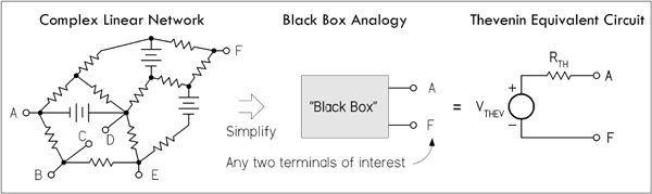
FIGURE 2.71 The essence of Thevenin’s theorem.
Luckily, a man by the name of Thevenin came up with a theorem, or trick, to simplify the problem and produce an answer—one that does not involve “hairy” mathematics. Using what Thevenin discovered, if only two terminals are of interest, these two terminals can be extracted from the complex circuit, and the rest of the circuit can be considered a black box. Now the only things left to work with are these two terminals. By applying Thevenin’s tricks (which you will see in a moment), you will discover that this black box, or any linear two-terminal dc network, can be represented by a voltage source in series with a resistor. (This statement is referred to as Thevenin’s theorem.) The voltage source is called the Thevenin voltage VTHEV, and the resistance is called the Thevenin resistance RTHEV; together, the two form what is called the Thevenin equivalent circuit. From this simple equivalent circuit you can easily calculate the current flow through a load placed across its terminals by using Ohm’s law: I = VTHEV/(RTHEV + RLOAD).
Note that circuit terminals (black box terminals) might actually not be present in a circuit. For example, instead, you may want to find the current and voltage across a resistor (RLOAD) that is already within a complex network. In this case, you must remove the resistor and create two terminals (making a black box) and then find the Thevenin equivalent circuit. After the Thevenin equivalent circuit is found, you simply replace the resistor (or place it across the terminals of the Thevenin equivalent circuit), calculate the voltage across it, and calculate the current through it by applying Ohm’s law again: I = VTHEV/(RTHEV + RLOAD). However, two important questions remain: What are the tricks? And what are VTHEV and RTHEV?
First, VTHEV is simply the voltage across the terminals of the black box, which can be either measured or calculated. RTHEV is the resistance across the terminals of the black box when all the dc sources (e.g., batteries) are replaced with shorts, and it, too, can be measured or calculated.
As for the tricks, we can generalize and say that the superposition theorem is involved. However, Thevenin figured out, using the tricks presented in the following example, that the labor involved with applying the superposition theorem (removing sources one at a time, calculating partial currents, and adding them, etc.) could be reduced by removing all sources at once, and finding the Thevenin resistance. An example is the best cure. See Fig. 2.72.
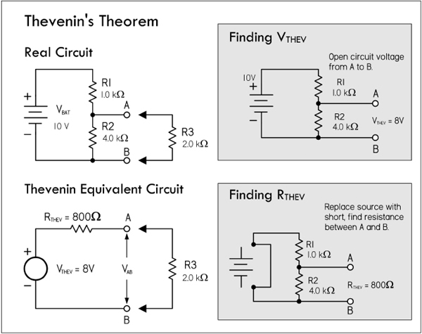
FIGURE 2.72 Here’s an example of how Thevenin’s theorem can be used in a voltage divider circuit to easily calculate the voltage across and the current flow through an attached load.
First remove the load R3 and open up the terminals of interest (A and B). Then, determine the Thevenin voltage VTHEV using Ohm’s law or the voltage divider equation—it’s the open-circuit voltage across A and B.
Next, calculate the Thevenin resistance RTHEV across the terminals A and B by replacing the dc source (VBAT) with a short and calculating or measuring the resistance across A and B. RTHEV is simply R1 and R2 in parallel.
The final Thevenin equivalent circuit is then simply VTHEV in series with RTHEV. The voltage across the load and the current through the load (R3) are:
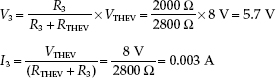
2.19.2 Norton’s Theorem
Norton’s theorem is another tool for analyzing complex networks. Like Thevenin’s theorem, it takes a complex two-terminal network and replaces it with a simple equivalent circuit. However, instead of a Thevenin voltage source in series with a Thevenin resistance, the Norton equivalent circuit consists of a current source in parallel with a resistance—which happens to be the same as the Thevenin resistance. The only new trick is finding the value of the current source, which is referred to as the Norton current INORTON. In essence, Norton’s theorem is to current sources as Thevenin’s theorem is to voltage sources. Its underlying mechanism, like that of Thevenin’s, is the superposition theorem.
Figure 2.73 shows how the circuit just analyzed by means of Thevenin’s theorem can be analyzed using Norton’s theorem. The Norton current INORTON represents the short-circuit current through terminals A and B.
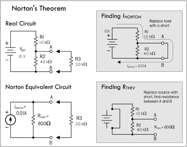
FIGURE 2.73 To find INORTON, first remove load R3 and replace it with a short. Using Ohm’s law, and noticing that no current will ideally flow through R2 since it’s shorted, you find the short-circuit current, or Norton current, to be:
Next, find the Thevenin resistance—simply use the result from the previous example:
RTHEV = 800 Ω.
The final Norton equivalent circuit can then be constructed. Replacing R3, you can now determine how much current will flow through R3, using Ohm’s law, or simply applying the current divider equation.
A Norton equivalent circuit can be transformed into a Thevenin equivalent circuit and vice versa. The equivalent resistor stays the same in both cases; it is placed in series with the voltage source in the case of a Thevenin equivalent circuit and in parallel with the current source in the case of the Norton equivalent circuit. The voltage for a Thevenin equivalent source is equal to the nonload voltage appearing across the resistor in the Norton equivalent circuit. The current for a Norton equivalent source is equal to the short-circuit current provided by the Thevenin source.
Examples: Find the Thevenin and Norton equivalent circuits for everything between points A and B for each of the four circuits in Fig. 2.74.
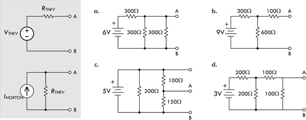
FIGURE 2.74
Answers: a: VTHEV = 2 V, RTHEV = 100 Ω, INORT = 0.02 A, b: VTHEV = 6 V, RTHEV = 300 Ω, INORT = 0.02 A, c: VTHEV = 3 V, RTHEV = 60 Ω, INORT = 0.05 A, d: VTHEV = 0.5 V, RTHEV = 67 Ω, INORT = 0.007 A
Example: Here’s an example where Thevenin’s theorem can be applied a number of times to simplify a complex circuit that has more than one source. In essence, you create Thevenin subcircuits and combine them. Often this is easier than trying to find the whole Thevenin equivalent circuit in one grand step. Refer to Fig. 2.75.
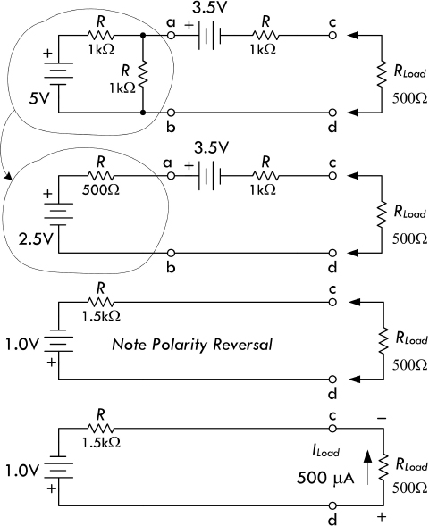
Here we’re interested in finding the current that will flow through a load resistor Rload when attached to terminals c and d. To simplify matters, first find the Thevenin equivalent circuit for everything to the left of a and b. Using the voltage divider and resistors-in-parallel formulas:
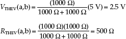
(Recall that we replaced the 5-V source with a short when finding RTHEV.)
Incorporating this equivalent circuit back into the main circuit, as shown in the second circuit down, we then determine the Thevenin equivalent circuit for everything to the left of c and d. Using Kirchhoff’s voltage law and resistors-in-series formulas:
VTHEV (c,d) = 2.5 V – 3.5 V = –1.0 V
(In terms of the diagram, this represents a polarity reversal, or simply flipping the battery.)
RTHEV (c,d) = 500 Ω + 1000 Ω = 1500 Ω
(Both sources were shorted to find RTHEV.)
Now we attach our load of 500 Ω and get the current:
FIGURE 2.75
Example: To increase the current capacity, batteries are placed in parallel. If the internal resistance is 0.2 Ω for each 1.5-V battery, find the equivalent Thevenin circuit. Refer to Fig. 2.76.
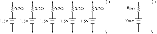
FIGURE 2.76
Answer: RTHEV = 0.04 Ω, VTHEV = 1.5 V. (Apply Thevenin’s theorem in steps.) As you can see, the net internal resistance of the Thevenin circuit is much less—a result of placing batteries in parallel.
2.20 AC Circuits
A circuit is a complete conductive path through which electrons flow from source to load and back to source. As we’ve seen, if the source is dc, electrons will flow in only one direction, resulting in a direct current (dc). Another type of source that is frequently used in electronics is an alternating source that causes current to periodically change direction, resulting in an alternating current (ac). In an ac circuit, not only does the current change directions periodically, the voltage also periodically reverses.
Figure 2.77 shows a dc circuit and an ac circuit. The ac circuit is powered by a sinusoidal source, which generates a repetitive sine wave that may vary in frequency from a few cycles per second to billions of cycles per second, depending on the application.
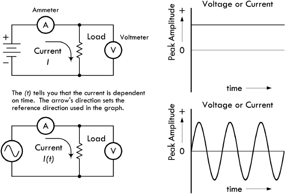
FIGURE 2.77
The positive and negative swings in voltage/current relative to a zero volt/amp reference line simply imply that the electromotive force of the source has switched directions, causing the polarity of the voltage source to flip, and forcing current to change directions. The actual voltage across the source terminals at a given instant in time is the voltage measured from the 0-V reference line to the point on the sinusoidal waveform at the specified time.
2.20.1 Generating AC
The most common way to generate sinusoidal waveforms is by electromagnetic induction, by means of an ac generator (or alternator). For example, the simple ac generator in Fig. 2.78 consists of a loop of wire that is mechanically rotated about an axis while positioned between the north and south poles of a magnet. As the loop rotates in the magnetic field, the magnetic flux through it changes, and charges are forced through the wire, giving rise to an effective voltage or induced voltage. According to Fig. 2.78, the magnetic flux through the loop is a function of the angle of the loop relative to the direction of the magnetic field. The resultant induced voltage is sinusoidal, with angular frequency ω (radians per second).
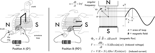
FIGURE 2.78 Simple ac generator.
Real ac generators are, of course, more complex than this, but they operate under the same laws of induction, nevertheless. Other ways of generating ac include using a transducer (e.g., a microphone) or even using a dc-powered oscillator circuit that uses special inductive and capacitive effects to cause current to resonate back and forth between an inductor and a capacitor.
Why Is AC Important?
There are several reasons why sinusoidal waveforms are important in electronics. The first obvious reason has to do with the ease of converting circular mechanical motion into induced current via an ac generator. However, another very important reason for using sinusoidal waveforms is that if you differentiate or integrate a sinusoid, you get a sinusoid. Applying sinusoidal voltage to capacitors and inductors leads to sinusoidal current. It also avoids problems on systems, a subject that we’ll cover later. But one of the most important benefits of ac involves the ability to increase voltage or decrease voltage (at the expense of current) by using a transformer. In dc, a transformer is useless, and increasing or decreasing a voltage is a bit tricky, usually involving some resistive power losses. Transformers are very efficient, on the other hand, and little power is lost in the voltage conversion.
2.20.2 Water Analogy of AC
Figure 2.79 shows a water analogy of an ac source. The analogy uses an oscillating piston pump that moves up and down by means of a cam mechanism, driven by a hand crank.
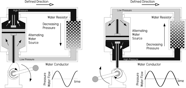
FIGURE 2.79
In the water analogy, water particles, on average, appear to simply swish back and forth as the crank is turned. In an ac electrical circuit, a similar effect occurs, though things are a bit more complex. One way to envision what’s going on is that within a conductor, the drift velocity of the sea of electrons is being swished back and forth in a sinusoidal manner. The actual drift velocity and distance over which the average drift occurs are really quite small (fractions of millimeter-per-second range, depending on conductor and applied voltage). In theory, this means that there is no net change in position of an “average” electron over one complete cycle. (This is not to be confused with an individual electron’s thermal velocity, which is mostly random, and at high velocity.) Also, things get even more complex when you start applying high frequencies, where the skin effect enters the picture—more on this later.
2.20.3 Pulsating DC
If current and voltage never change direction within a circuit, then from one perspective, we have a dc current, even if the level of the dc constantly changes. For example, in Fig. 2.80, the current is always positive with respect to 0, though it varies periodically in amplitude. Whatever the shape of the variations, the current can be referred to as “pulsating dc.” If the current periodically reaches 0, it is referred to as “intermittent dc.”
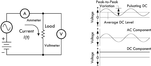
FIGURE 2.80
From another perspective, we may look at intermittent and pulsating dc as a combination of an ac and a dc current. Special circuits can separate the two currents into ac and dc components for separate analysis or use. There are also circuits that combine ac and dc currents and voltages.
2.20.4 Combining Sinusoidal Sources
Besides combining ac and dc voltages and currents, we can also combine separate ac voltages and currents. Such combinations will result in complex waveforms. Figure 2.81 shows two ac waveforms fairly close in frequency, and their resultant combination. The figure also shows two ac waveforms dissimilar in both frequency and wavelength, along with the resultant combined waveform.
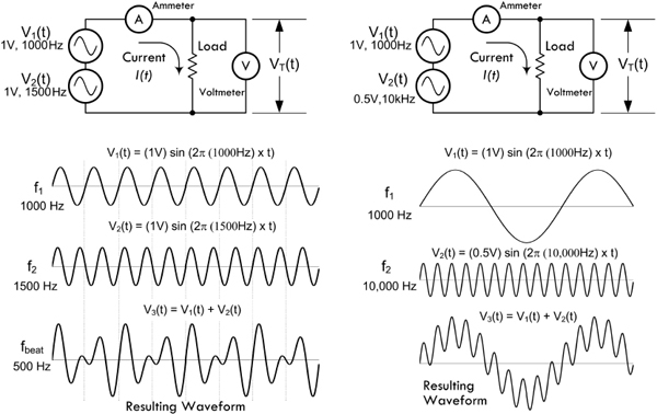
FIGURE 2.81 (Left) Two ac waveforms of similar magnitude and close in frequency form a composite wave. Note the points where the positive peaks of the two waves combine to create high composite peaks: this is the phenomenon of beats. The beat note frequency is f2 – f1 = 500 Hz. (Right) Two ac waveforms of widely different frequencies and amplitudes form a composite wave in which one wave appears to ride upon the other.
Later we will discover that by combining sinusoidal waveforms of the same frequency—even though their amplitudes and phases may be different—you always get a resultant sine wave. This fact becomes very important in ac circuit analysis.
2.20.5 AC Waveforms
Alternating current can take on many other useful wave shapes besides sinusoidal. Figure 2.82 shows a few common waveforms used in electronics. The squarewave is vital to digital electronics, where states are either true (on) or false (off). Triangular and ramp waveforms—sometimes called sawtooth waves—are especially useful in timing circuits. As we’ll see later in the book, using Fourier analysis, you can create any desired shape of periodic waveform by adding a collection of sine waves together.
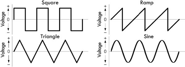
FIGURE 2.82
An ideal sinusoidal voltage source will maintain its voltage across its terminals regardless of load—it will supply as much current as necessary to keep the voltage the same. An ideal sinusoidal current source, on the other hand, will maintain its output current, regardless of the load resistance. It will supply as much voltage as necessary to keep the current the same. You can also create ideal sources of other waveforms. Figure 2.83 shows schematic symbols for an ac voltage source, an ac current source, and a clock source used to generate squarewaves.
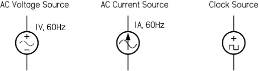
FIGURE 2.83
In the laboratory, a function generator is a handy device that can be used to generate a wide variety of waveforms with varying amplitudes and frequencies.
2.20.6 Describing an AC Waveform
A complete description of an ac voltage or current involves reference to three properties: amplitude (or magnitude), frequency, and phase.
Figure 2.84 shows the curve of a sinusoidal waveform, or sine wave. It demonstrates the relationship of the voltage (or current) to relative positions of a circular rotation through one complete revolution of 360°. The magnitude of the voltage (or current) varies with the sine of the angle made by the circular movement with respect to the zero point. The sine of 90° is 1, which is the point of maximum current (or voltage); the sine of 270° is −1, which is the point of maximum reverse current (or voltage); the sine of 45° is 0.707, and the value of current (or voltage) at the 45° point of rotation is 0.707 times the maximum current (or voltage).

FIGURE 2.84
2.20.7 Frequency and Period
A sinusoidal waveform generated by a continuously rotating generator will generate alternating current (or voltage) that will pass through many cycles over time. You can choose an arbitrary point on any one cycle and use it as a marker—say, for example, the positive peak. The number of times per second that the current (or voltage) reaches this positive peak in any one second is called the frequency of the ac. In other words, frequency expresses the rate at which current (or voltage) cycles occur. The unit of frequency is cycles per second, or hertz—abbreviated Hz (after Heinrich Hertz).
The length of any cycle in units of time is the period of the cycle, as measured from two equivalent points on succeeding cycles. Mathematically, the period is simply the inverse of the frequency:
(2.22)
and
(2.23)
Answer:
Example: What is the frequency of an ac voltage that has period of 2 ns?
Answer:
The frequency of alternating current (or voltage) in electronics varies over a wide range, from a few cycles per second to billions of cycles per second. To make life easier, prefixes are used to express large frequencies and small periods. For example: 1000 Hz = 1 kHz (kilohertz), 1 million hertz = 1 MHz (megahertz), 1 billion hertz = 1 GHz (gigahertz), 1 trillion hertz = 1 THz (terahertz). For units smaller than 1, as in the measurements of period, the basic unit of a second can become millisecond (1 thousandth of a second, or ms), microsecond (1 millionth of a second, or μs), nanosecond (1 billionth of a second, or ns), and picosecond (1 trillionth of a second, or ps).
2.20.8 Phase
When graphing a sine wave of voltage or current, the horizontal axis represents time. Events to the right on the graph take place later, while events to the left occur earlier. Although time can be measured in seconds, it actually becomes more convenient to treat each cycle of a waveform as a complete time unit, divisible by 360°. A conventional starting point for counting in degrees is 0°—the zero point as the voltage or current begins a positive half cycle. See Fig. 2.85a.
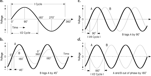
FIGURE 2.85 (a) An ac cycle is divided into 360° that are used as a measure of time or phase. (b) When two waves of the same frequency start their cycles at slightly different times, the time difference or phase difference is measured in degrees. In this drawing, wave B starts 45° (one-eighth cycle) later than wave A, and so lags 45° behind A. (c and d) Two special cases of phase difference: In (c) the phase difference between A and B is 90°; in (d) the phase difference is 180°.
By measuring the ac cycle this way, it is possible to do calculations and record measurements in a way that is independent of frequency. The positive peak voltage or current occurs at 90° during a cycle. In other words, 90° represents the phase of the ac peak relative to the 0° starting point.
Phase relationships are also used to compare two ac voltage or current waveforms at the same frequency, as shown in Fig. 2.85b. Since waveform B crosses the zero point in the positive direction after A has already done so, there is a phase difference between the two waveforms. In this case, B lags A by 45°; alternatively, we can say that A leads B by 45°. If A and B occur in the same circuit, they add together, producing a composite sinusoidal waveform at an intermediate phase angle relative to the individual waveforms. Interestingly, adding any number of sine waves of the same frequency will always produce a sine wave of the same frequency—though the magnitude and phase may be unique.
In Fig. 2.85c we have a special case where B lags A by 90°. B’s cycle begins exactly one-quarter cycle after A’s. As one waveform passes through zero, the other just reaches its maximum value.
Another special case occurs in Fig. 2.85d, where waveforms A and B are 180° out of phase. Here it doesn’t matter which waveform is considered the leading or lagging waveform. Waveform B is always positive when waveform A is negative, and vice versa. If you combine these two equal voltage or current waveforms together within the same circuit, they completely cancel each other out.
2.21 AC and Resistors, RMS Voltage, and Current
Alternating voltages applied across a resistor will result in alternating current through the resistor that is in phase with the voltage, as seen in Fig. 2.86. Given the ac voltage and resistance, you can apply Ohm’s law and find the ac current. For example, a sinusoidal waveform generated by a function generator can be mathematically described by:
(2.24)
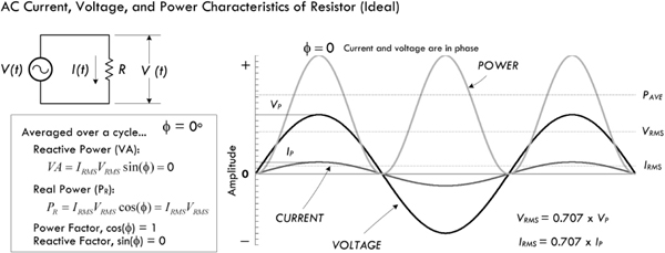
FIGURE 2.86
where VP is the peak amplitude of the sinusoidal voltage waveform, f is the frequency, and t is the time. Using Ohm’s law and the power law, you get the following:
(2.25)
If you graph both V(t) and I(t) together, as shown in Fig. 2.86, you notice that the current and the voltage are in phase with each other. As the voltage increases in one direction, the current also increases in the same direction. Thus, when an ac source is connected to a purely resistive load, the current and voltage are in phase. If the load isn’t purely resistive (e.g., has capacitance and inductance), it’s a whole different story—more on that later.
To find the power dissipated by the resistor under sinusoidal conditions, we can simply plug the sinusoidal voltage expression into Ohm’s power law to get an instantaneous power expression:
(2.26)
Expressing voltage, current, and power in an instantaneous fashion is fine, mathematically speaking; however, in order to get a useful result, you need to plug in a specific time—say, t = 1.3 s. But how often do you need to know that the voltage, current, or power are at exactly t = 1.3 s? Better yet, when do you start counting? These instantaneous values are typically inconvenient for any practical use. Instead, it is more important to come up with a kind of averaging scheme that can be used to calculate effective power dissipation without dealing with sinusoidal functions.
Now, you might be clever and consider averaging the sinusoidal voltage or current over a complete cycle to get some meaningful value. However, the average turns out to be zero—positive and negative sides of waveforms cancel. This may be a bit confusing, in terms of power, since the positive-going part of the wave still delivers energy, as does the negative-going part. If you’ve ever received a shock from 120-V line voltage, you’ll be able to attest to that.
The measurement that is used instead of the average value is the RMS or root mean square value, which is found by squaring the instantaneous values of the ac voltage or current, then calculating their mean (i.e., their average), and finally taking the square root of this—which gives the effective value of the ac voltage or current. These effective, or RMS, values don’t average out to zero and are essentially the ac equivalents of dc voltages and currents. The RMS values of ac voltage and current are based upon equating the values of ac and dc power required to heat a resistive element to exactly the same degree. The peak ac power required for this condition is twice the dc power needed. Therefore, the average ac power equivalent to a corresponding average dc power is half the peak ac power.
(2.27)
Mathematically, we can determine the RMS voltage and current values for sinusoidal waveforms V(t) = VP sin (2π × f × t), and I(t) = IP sin (2π × f × t):
(2.28) RMS voltage
(2.29) RMS current
Notice that the RMS voltage and current depend only on the peak voltage or current—they are independent of time or frequency. Here are the important relations, without the scary calculus:
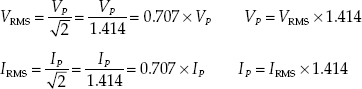
For example, a U.S. electric utility provides your home with 60 Hz, 120 VAC (in Europe and many other countries it’s 50 Hz, 240V AC). The “VAC” unit tells you that the supplied voltage is given in RMS. If you were to attach an oscilloscope to the outlet, the displayed waveform on the screen would resemble the following function: V(t) = 170 V sin (2π × 60 Hz × t), where 170 V is the peak voltage.
With our new RMS values for voltage and current, we can now substitute them into Ohm’s law to get what’s called ac Ohm’s law:
(2.30) ac Ohm’s law
Likewise, we can use the RMS voltage and current and substitute them into Ohm’s power law to get what’s called the ac power law, which gives the effective power dissipated (energy lost per second):
(2.31) ac power law
Again, these equations apply only to circuits that are purely resistive, meaning there is virtually no capacitance and/or inductance. Doing power calculation on circuits with inductance and capacitance is a bit more complicated, as we’ll see a bit later.
Figure 2.87 shows the relationships between RMS, peak, peak-to-peak and half-wave average values of voltage and current. Being able to convert from one type to another is important, especially when dealing with component maximum voltage and current ratings—sometimes you’ll be given the peak value, other times the RMS value. Understanding the differences also becomes crucial when making test measurements—see the note on pages 91–92 about making RMS test measurements. Most of the time, when dealing with ac voltage you can assume that voltage is expressed as an RMS value unless otherwise stated.
Conversion Factors for AC Voltage and Current
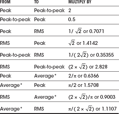
* Represents average over half a cycle.
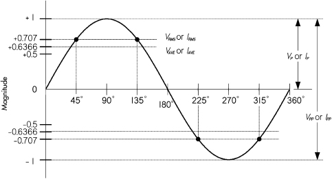
FIGURE 2.87
Example 1: How much current would flow through a 100-Ω resistor connected across the hot and neutral sockets of a 120-VAC outlet? How much power would be dissipated? What would the results be using 1000-Ω, 10,000-Ω, and 100,000-Ω resistors?
Answer:
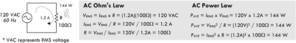
FIGURE 2.88
First, don’t try this with any ordinary resistor; you’d need a power resistor or special heating element with a power rating of greater than 144 W! (Also, simply don’t attempt attaching a resistor with the outlets powered.) A 1000-Ω resistor plugged into the same outlet would dissipate 14.4 W; a 10,000-Ω resistor would dissipate 1.44 W; a 100,000-Ω resistor would dissipate 0.14 W.
Example 2: What is the peak voltage on a capacitor if the RMS voltage of a sinusoidal waveform signal across it is 10.00 VAC?
Answer: VAC means RMS, so VP =  × VRMS = 1.414 × 10 V = 14.14 V.
Example 3: A sinusoidal voltage displayed on an oscilloscope has a peak amplitude of 3.15 V. What is the RMS value of the waveform?
Example 4: A 200-W resistive element in a heater is connected to a 120-VAC outlet. How much current is flowing through the resistive element? What’s the resistance of the element, assuming it’s an ideal resistor?
Answer: IRMS = PAVE/VRMS = 200 W/120 VAC = 1.7 A. R = VRMS/IRMS = 120 V/1.7 A = 72 Ω.
Example 5: A sinusoidal voltage supplied by a function generator is specified as 20 V peak to peak at 1000 Hz. What is the minimum resistance value of a-W resistor you can place across the generator’s output before exceeding the resistor’s power rating?
Answer: VP = 1/2 VP−P = 10 V; VRMS = 0.707 × VP = 7.1 VAC; R = VRMS2/PAVE = (7.1)2/(1/8 W) = 400 Ω.
Example 6: The output of an oscillator circuit is specified as 680 mVAC. If you feed this into an op amp with an input resistance of 10 MΩ, how much current enters the IC?
Answer: IRMS = VRMS/R = 0.68 V/(10,000,000 Ω) = 0.000000068 = 68 nA.
MEASURING RMS VOLTAGES AND CURRENTS
There are many digital multimeters that do not measure the RMS value of an ac voltage directly. Often the meter will simply measure the peak value and calculate the equivalent RMS value—assuming the measured waveform is sinusoidal—and then display this value. Analog meters usually measure the half-wave average value, but are made to indicate the equivalent RMS.
True RMS multimeters, on the other hand, measure the true RMS value of voltages and current, and are especially handy for nonsinusoidal voltage and currents. Though relatively expensive, these meters are worth the price. It’s important to note that true RMS meters will also include the contribution of any dc voltages or current components present along with the ac.
Fortunately, you can still get a fairly accurate idea of the RMS value of a sine waveform, knowing one of the other measurements such as the half-wave average, peak, or peak-to-peak value. This can be done by calculation, or using the table in Fig. 2.89. As you can see, it’s also possible to work out the RMS value of a few other symmetrical and regular waveforms, such as square and triangular waves, knowing their peak, average, or peak-to-peak values.
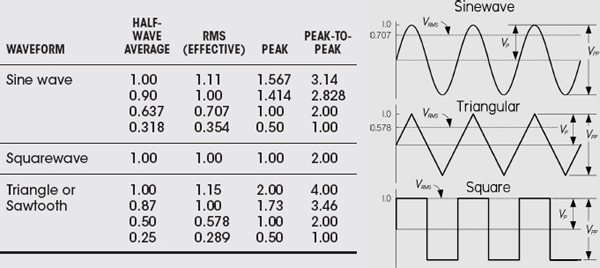
FIGURE 2.89
An important thing to note when using the table is that you need to know the exact basis on which your meter’s measurement is made. For example, if your meter measures the peak value, and then calculates and displays the equivalent sine wave RMS figure, this means you’ll need to use the table differently when compared to the situation where the meter really measures the half-wave average and calculates the sine wave RMS figure from that. So take care, especially if you’re not sure exactly how your meter works.
2.22 Mains Power
In the United States, three wires run from the pole transformers (or underground or surface enclosed transformer) to the main service panel at one’s home. One wire is the A-phase wire (usually black in color), another is the B-phase wire (usually black in color), and the third is the neutral wire (white in color). Figure 2.90 shows where these three wires originate from the pole transformer. The voltage between the A-phase and the B-phase wires, or the hot-to-hot voltage, is 240 V, while the voltage between the neutral wire and either the A-phase or the B-phase wire, or the neutral-to-hot voltage, is 120 V. (These voltages are nominal and may vary from region to region, say 117 V instead of 120 V.)
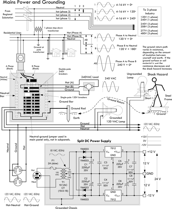
FIGURE 2.90
At the home, the three wires from the pole/green box transformer are connected through a wattmeter and then enter a main service panel that is grounded to a long copper rod driven into the ground or to the steel in a home’s foundation. The A-phase and B-phase wires that enter the main panel are connected through a main disconnect breaker, while the neutral wire is connected to a terminal referred to as the neutral bar or neutral bus. A ground bar also may be present within the main service panel. The ground bar is connected to the grounding rod or to the foundation’s steel supports.
Within the main service panel, the neutral bar and the ground bar are connected together (they act as one). However, within subpanels (service panels that get their power from the main service panel but which are located some distance from the main service panel), the neutral and ground bars are not joined together. Instead, the subpanel’s ground bar receives a ground wire from the main services panel. Often the metal conduit that is used to transport the wires from the main service panel to the subpanel is used as the ground wire. However, for certain critical applications (e.g., computer and life-support systems), the ground wire probably will be included within the conduit. Also, if a subpanel is not located in the same building as the main panel, a new ground rod typically is used to ground the subpanel. Note that different regions within the United States may use different wiring protocols. Therefore, do not assume that what I am telling you is standard practice where you live. Contact your local electrical inspector.
Within the main service panel, there are typically two bus bars into which circuit breaker modules are inserted. One of these bus bars is connected to the A-phase wire; the other bus bar is connected to the B-phase wire. To power a group of 120-V loads (e.g., upstairs lights and 120-V outlets), you throw the main breaker to the off position and then insert a single-pole breaker into one of the bus bars. (You can choose either the A-phase bus bar or the B-phase bus bar. The choice of which bus bar you use becomes important only when it comes to balancing the overall load—more on that in a moment.) Next, you take a 120-V three-wire cable and connect the cable’s black (hot) wire to the breaker, connect the cable’s white (neutral) wire to the neutral bar, and connect the cable’s ground wire (green or bare) to the ground bar. You then run the cable to where the 120-V loads are located, connect the hot and neutral wires across the load, and fasten the ground wire to the case of the load (typically a ground screw is supplied on an outlet mounting or light figure for this purpose). To power other 120-V loads that use their own breakers, you basically do the same thing you did in the last setup. However, to maximize the capacity of the main panel (or subpanel) to supply as much current as possible without overloading the main circuit breaker in the process, it is important to balance the total load current connected to the A-phase breakers with the total load current connected to the B-phase breakers. This is referred to as “balancing the load.”
Now, if you want to supply power to 240-V appliances (ovens, washers, etc.), you insert a double-pole breaker between the A-phase and B-phase bus bars in the main (or subpanel). Next, you take a 240-V three-wire cable and attach one of its hot wires to the A-phase terminal of the breaker and attach its other hot wire to the B-phase terminal of the breaker. The ground wire (green or bare) is connected to the ground bar. You then run the cable to where the 240-V loads are located and attach the wires to the corresponding terminals of the load (typically within a 240-V outlet). Also, 120-V/240-V appliances are wired in a similar manner, except you use a four-wire cable that contains an additional neutral (white) wire that is joined at the neutral bar within the main panel (or subpanel).
In addition, in many places, modifications to mains wiring must be carried out or checked by a certified electrician. As a note of caution, do not attempt home wiring unless you are sure of your abilities. If you feel that you are capable, just make sure to flip the main breaker off before you start work within the main service panel. When working on light fixtures, switches, and outlets that are connected to an individual breaker, tag the breaker with tape so that you do not mistakenly flip the wrong breaker when you go back to test your connections.
2.23 Capacitors
If you take two oppositely charged parallel conducting plates separated a small distance apart by an insulator—such as air or a dielectric such as ceramic—you have created what’s called a capacitor. Now, if you apply a voltage across the plates of the capacitor using a battery, as shown in Fig. 2.91, an interesting thing occurs. Electrons are pumped out the negative battery terminal and collect on the lower plate, while electrons are drawn away from the upper plate into the positive battery terminal. The top plate becomes deficient in electrons, while the lower plate becomes abundant in electrons.
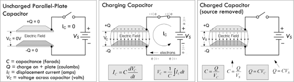
FIGURE 2.91
Very quickly, the top plate reaches a positive charge +Q and the negative plate reaches a negative charge −Q. Accompanying the charge is a resultant electric field between the plates and a voltage equal to the battery voltage.
The important thing to notice with our capacitor is that when we remove the voltage source (battery), the charge, electric field, and corresponding voltage (presently equal to the battery voltage) remain. Ideally, this state of charge will be maintained indefinitely. Even attaching an earth ground connection to one of the plates—doesn’t matter which one—will not discharge the system. For example, attaching an earth ground to the negative terminal doesn’t cause the electrons within that plate to escape to the earth ground where neutral charge is assumed. (See Fig. 2.92.)
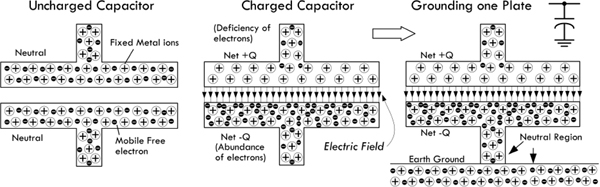
FIGURE 2.92
It might appear that the abundance of electrons would like to escape to the earth ground, since it is at a lower potential (neutral). However, the electric field that exists within the capacitor acts like a glue; the positive charge on the upper plate “holds” onto the abundance of electrons on the negative plate. In other words, the positive plate induces a negative charge in the grounded plate.
In reality, a real-life charged capacitor that is charged and removed from the voltage source would eventually lose its charge. The reason for this has to do with the imperfect insulating nature of the gas or dielectric that is placed between the plates. This is referred to as leakage current and, depending on the construction of the capacitor, can discharge a capacitor within as little as a few seconds to several hours, if the source voltage is removed.
To quickly discharge a capacitor you can join the two plates together with a wire, which creates a conductive path for electrons from the negative plate to flow to the positive plate, thus neutralizing the system. This form of discharge occurs almost instantaneously.
The ratio of charge on one of the plates of a capacitor to the voltage that exists between the plates is called capacitance (symbolized C):
(2.32) Capacitance related to charge and voltage
C is always taken to be positive, and has units of farads (abbreviated F). One farad is equal to one coulomb per volt:
1 F = 1 C/1 V
Devices that are specifically designed to hold charge (electrical energy in the form of an electric field) are called capacitors. Figure 2.93 shows various symbols used to represent capacitors, along with a real capacitor model that we’ll discuss a bit later.
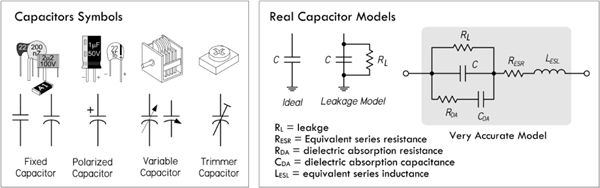
FIGURE 2.93
The equation C = Q/V is a general one; it really doesn’t tell you why one capacitor has a larger or smaller capacitance than another. However, in practice, when you buy a capacitor all you’ll be interested in is the capacitance value labeled on the device. (A voltage rating and other parameters are important, too, but we’ll talk about them later.) Most commercial capacitors are limited to a range from 1 pF (1 × 10⁻¹² F) to 4700 μF (1 × 10⁻⁶ F), with typical values for the first two digits of the capacitance of 10, 12, 15, 18, 22, 27, 33, 39, 47, 56, 68, 82, 100. (Examples: 27 pF, 100 pF, 0.01 μF, 4.7 μF, 680 μF).
Having a wide range of capacitances allows you to store different amounts of charge for a given potential difference, as well as maintaining different potential differences for a given charge. With the appropriate capacitor, you can therefore control the storage and delivery of charge, or control potential differences.
Example 1: Five volts are applied across a 1000-μF capacitor until the capacitor is fully charged. How much charge exists on the positive and negative plates?
Answer: Q = CV = (1000 × 10−6 F)(5 V) = 5 × 10⁻³ C. This is the charge on the positive plate. The charge on the negative plate is the same, but opposite in sign.
Example 2: A 1000-μF capacitor and a 470-μF capacitor are arranged in the circuit shown in Fig. 2.94, with a 10-V dc supply. Initially, the switch is at position B then thrown to position A, and then thrown to position B, and then to position A, and finally to position B. Assuming the capacitors have enough time to fully charge or discharge during the interval between switches, what is the final voltage across each capacitor after the last switch takes place?

FIGURE 2.94
Answer: When the switch is thrown from B to A the first time, C1 charges to:
Q1 = C1V = (1000 × 10−6 F)(10 V) = 0.01 C
When the switch is then thrown to B, the circuit becomes essentially one big capacitor equal to C1 + C2 or 1470 μF. Charge will flow from C1 to C2, since the system wants to go to the lowest energy configuration. The charge on each capacitor is the percentage of capacitance to the total capacitance for each capacitor multiplied by the initial charge on C1 before the switch was thrown to position B:
The voltage at the new equilibrium is:
V1 = Q1/C1 = 0.0068/1000 μF = 6.8 V
V2 = Q2/C2 = 0.0032/470 μF = 6.8 V
The rest of the results are obtained in using similar calculations—the final result yields 9.0 V, as shown in the graph to the right.
We could be content with this limited knowledge. However, if you want to build your own capacitors, as well as understand time-dependent behavior, such as displacement current and capacitive reactance, a deeper understanding of capacitance is needed.
2.23.1 Determining Capacitance
The capacitance of a capacitor is determined by plate area A, plate separation d, and insulating material or dielectric. If a voltage V is applied between two parallel plates, an electric field equal to E = V/d will be produced. From Gauss’s law, each plate must contain an equal and opposite charge given by:
(2.33)
where ε is the permittivity of the dielectric. Free space (vacuum) has a permittivity given by:
(2.34)
The constant εA/d term in the equation is the capacitance,
(2.35)
The relative permittivity of a material referenced to the permittivity in vacuum is referred to as the dielectric constant, which is given by:
Plugging this into the previous expression, we get the capacitance in terms of dielectric constant:
(2.36)
where C is in farads, A is in meters squared, and d is in meters.
The dielectric constant varies from 1.00059 for air (1 atm) to over 105 for some types of ceramic. Table 2.6 shows relative dielectric constants for various materials often used in constructing capacitors.
Capacitors often have more than two plates, the alternate plates being connected to form two sets, as shown in the lower drawing in Fig. 2.95. This makes it possible to obtain a fairly large capacitance in a small space. For a multiple-plate capacitor, we use the following expression to find the capacitance:
(2.37)

FIGURE 2.95
where the area A is in meters squared, the separation d is in meters, and the number of plates n is an integer.
Example: What is the capacitance of a multiple-plate capacitor containing two plates, each with an area of 4 cm2, a separation of 0.15 mm, and a paper dielectric?
Answer:
2.23.2 Commercial Capacitors
Commercial capacitors, like those shown in Fig. 2.95, are constructed from plates of foil with a thin solid or liquid dielectric sandwiched between, so relatively large capacitance can be obtained in a small unit. The solid dielectrics commonly used are mica, paper, polypropylene, and special ceramics.
Electrolytic capacitors use aluminum-foil plates with a semiliquid conducting chemical compound between them. The actual dielectric is a very thin film of insulating material that forms on one set of the plates through electrochemical action when a dc voltage is applied to the capacitor. The capacitance obtained with a given area in an electrolytic capacitor is very large compared to capacitors having other dielectrics, because the film is so thin—much less than any thickness practical with a solid dielectric. Electrolytic capacitors, due to the electrochemical action, require that one lead be placed at a lower potential than the other. The negative lead (−) is indicated on the package, and some surface mount electrolytics mark the positive end. This polarity adherence means that, with the exception of special nonpolarized electrolytics, electrolytic capacitors shouldn’t be used in ac applications. It is okay to apply a superimposed ac signal riding upon a dc voltage, provided the peak voltage doesn’t exceed the maximum dc voltage rating of the electrolytic capacitor.
2.23.3 Voltage Rating and Dielectric Breakdown
The dielectric within a capacitor acts as an insulator—its electrons do not become detached from atoms the way they do in conductors. However, if a high enough voltage is applied across the plates of the capacitor, the electric field can supply enough force on electrons and nuclei within the dielectric to detach them, resulting in a breakdown in the dielectric. Failed dielectrics often puncture and offer a low-resistance current path between the two plates.
The breakdown voltage of a dielectric depends on the dielectric’s chemical composition and thickness. A gas dielectric capacitor breakdown is displayed as a spark or arc between the plates. Spark voltages are typically given in units of kilovolts per centimeter. For air, the spark voltage may range from 100 kV/cm for gaps as narrow as 0.005 cm to 30 kV/mm for gaps as wide as 10 cm. Other things that contribute to the exact breakdown voltage level are electrode shape, gap distance, air pressure or density, the voltage, impurities within the dielectric, and the nature of the external circuit (air humidity, temperature, etc.).
Dielectric breakdown can occur at a lower voltage between points or sharp-edged surfaces than between rounded and polished surfaces, since electric fields are more concentrated at sharp projections. This means that the breakdown voltage between metal plates can be increased by buffing the edges to remove any sharp irregularities. If a capacitor with a gas dielectric, such as air, experiences breakdown, once the arc is extinguished, the capacitor can be used again. However, if the plates become damaged due to the spark, they may require polishing, or the capacitor may need to be replaced. Capacitors with solid dielectrics are usually permanently damaged if there is dielectric breakdown, often resulting in a short or even an explosion.
Manufacturers provide what’s called a dielectric withstanding voltage (dwv), expressed in voltage per mil (0.001 in) at a specified temperature. They also provide a dc working voltage (dcwv) that takes into account other factors such as temperature and safety margin, which gives you a guideline to the maximum safe limits of dc voltage that can be applied before dielectric breakdown. The dcwv rating is most useful in practice.
As a rule of thumb, it is not safe to connect a capacitor across an ac power line unless it is designed for it. Most capacitors with dc ratings may short the line. Special ac-rated capacitors are available for such tasks. When used with other ac signals, the peak value of ac voltage should not exceed the dc working voltage.
2.23.4 Maxwell’s Displacement Current
An interesting thing to notice with our parallel-plate capacitor is that current appears to flow through the capacitor as it is charging and discharging, but doesn’t flow under steady dc conditions. You may ask: How is it possible for current to flow through a capacitor, ever, if there is a gap between the plates of the capacitor? Do electrons jump the gap? As it turns out, no actual current (or electron flow) makes it across the gap, at least in an ideal capacitor.
As we calculated a moment ago using Gauss’s law, the charge on an air-filled capacitor plate can be expressed in terms of the electric field, area, and permittivity of free space:
(2.38)
Some time ago, Scottish physicist James Clerk Maxwell (1831–1879) noted that even if no real current passed from one capacitor plate to the other, there was nevertheless a changing electric flux through the gap of the capacitor that increased and decreased with the magnitude and direction of the electric flux. (Electric flux for a parallel-plate capacitor is approximated by ΦE = EA, while a changing electric flux is expressed as dΦE/dt). Maxwell believed the electric flux permeated the empty space between the capacitor plates and induced a current in the other plate. Given the state of knowledge of electrodynamics at the time, he envisioned a displacement current (which he coined) crossing the empty gap, which he associated with a kind of stress within the ether (accepted at the time)—the “stress” being electric and magnetic fields. (The displacement current helped supply Maxwell with the missing component to complete a set of electromagnetic formulas known as Maxwell’s equations.) He associated the displacement current with displacements of the ether. With a bit of theoretical reckoning, as well as some help from some experimental data, he came up with the following equation, known as the displacement current, to explain how current could appear to enter one end of a capacitor and come out the other end.
(2.39)
Maxwell’s displacement expression appears to provide the correct answer, even though his notion of the ether has lost favor in the realm of physics. Modern physics provides a different model for displacement current than that envisioned by Maxwell and his ether. Nevertheless, the results obtained using Maxwell’s equation closely correlate with experiment.
As a side note, there also exists a magnetic field due to the displacement current, as shown in the drawing on the right in Fig. 2.96. You can calculate the magnetic field using what’s called Maxwell’s generalized form of Ampere’s law; however, the size of the magnetic field turns out to be so small that it essentially has no practical influence when compared to the electric field.
FIGURE 2.96
However deep you go when trying to explain the physical phenomena within a capacitor, such as using Maxwell’s equations or even modern physics, the practical equations that are useful in electronics really don’t require such detail. Instead, you can simply stick with using the following charge-based model.
Though Maxwell’s displacement current provides a model to explain the apparent current flow through a capacitor in terms of changing electric fields, it really isn’t needed to define capacitor performance. Instead, we can treat the capacitor as a black box with two leads, and define some rules relating the current entering and exiting the capacitor as the applied voltage across the capacitor changes. We don’t need to worry about the complex physical behavior within.
Now, the question remains: how do we determine the rules if we don’t understand the complex behavior within? Simple—we use the general definition of capacitance and the general definition of current, and combine the two. Though the mathematics for doing this is simple, understanding why this makes logical sense is not entirely obvious. The following parallel-plate example provides an explanation. Refer to Fig. 2.97.
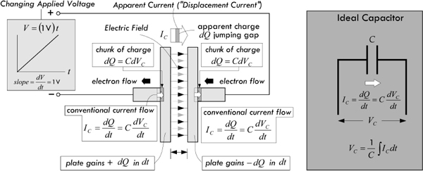
FIGURE 2.97
If we work in differentials (small changes), we can rewrite the general expression for capacitance as dQ = CdV, where C remains constant (with charge, voltage, or time). The general expression for current is I = dQ/dt, which, when combined with the last differential expression of capacitance, provides the expression:
(2.40) Apparent current “through” capacitor
Looking at Fig. 2.97, a “small” chunk dQ, which is equal to CdVc, enters the right plate during dt, while an equal-sized chunk exits the left plate. So a current equal to dQ/dt = CdVc/dt enters the left plate while an equal-sized current exits the right plate. (Negative electrons flow in the opposite direction.) Even though no actual current (or electrons) passes across the gap, Eq. 2.40 makes it appear that it does. After our little exercise using differentials, however, we can see that there is really no need to assume that a current must flow across the gap to get an apparent current flow “through” the capacitor.
Moving on, we can take the capacitor current expression just derived, rearrange things, and solve for the voltage across the capacitor:
(2.41) Voltage across capacitor
It’s important to note that these equations are representative of what’s defined as an ideal capacitor. Ideal capacitors, as the equation suggests, have several curious properties that are misleading if you are dealing with real capacitors. First, if we apply a constant voltage across an ideal capacitor, the capacitor current would be zero, since the voltage isn’t changing (dV/dt = 0). In a dc circuit, a capacitor thus acts like an open circuit. On the other hand, if we try to change the voltage abruptly, from 0 to 9 V, the quantity dV/dt = 9 V/0 V = infinity and the capacitor current would have to be infinite (see Fig. 2.98). Real circuits cannot have infinite currents, due to resistivity, available free electrons, inductance, capacitance, and so on, so the voltage across the capacitor cannot change abruptly. A more accurate representation of a real capacitor, considering construction and materials, looks like the model shown in Fig. 2.93.
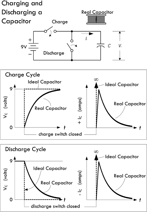
Under steady-state dc, a capacitor cannot pass current. It can only store or discharge charge (which it collects from current) when the voltage across it changes. Here, when the “charge switch” is closed (shorted), the 9-V battery voltage is applied instantly across the capacitor. In a real capacitor, the capacitor charges up to its maximum value practically instantly. But upon closer examination, the charge takes time to build up, due to internal resistance, meaning the displacement current cannot reach infinity. Instead, the current jumps to Vbattery/Rinternal and quickly drops exponentially as the capacitor reaches full charge, during which the voltage rises exponentially until it levels off at the applied voltage. The graph to the left shows voltage and current curves as the capacitor charges up. Note the impossible behavior that an ideal treatment of a capacitor introduces.
When the discharge switch is closed, a conductive path from positive to negative plate is made, and charge electrons will flow to the plate with a deficiency of electrons. The current that results is in the opposite direction as the charging current, but resembles it in that it initially peaks to a value of Vbattery/Rinternal and decays as the charge neutralizes. The voltage drops exponentially in the process.
FIGURE 2.98
If the equations for an ideal capacitor are screwy, what do we do for real-life calculations? For the most part, you don’t have to worry, because the capacitor will be substituted within a circuit that has resistance, which eliminates the possibility of infinite currents. The circuit resistance is also usually much greater than the internal resistance of the capacitor, so that the internal resistance of the capacitor can typically be ignored. In a minute, we’ll see a few resistor-capacitor circuits that will demonstrate this.
For those of you who are having problems with the previous explanations of apparent or displacement current, perhaps the following water analogy will help. Take it with a grain of salt, however, since what’s going on in a real capacitor isn’t analogous in all regards. Refer to Fig. 2.99.
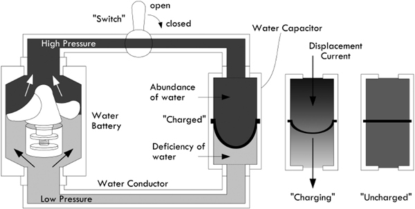
FIGURE 2.99
The water capacitor in Fig. 2.99 resembles a tube with a rubber membrane in the middle. The rubber membrane is somewhat analogous to the insulator or dielectric of a capacitor, while each separate compartment is analogous to each plate of a capacitor. If there is no pressure (analogous to voltage) across the water capacitor, each compartment contains the same amount of water (analogous to the number of free electrons). However, if pressure is suddenly applied across the water capacitor, the pressure within the top chamber increases, causing the membrane to expand downward, displacing water out from the lower chamber. Even though no water from the top makes it through the membrane, it appears as though current flows through the water capacitor, since the membrane is pushing the water within the lower chamber out. This is analogous to displacement current. Increasing the chamber size and altering the membrane strength are analogous to changing the capacitance and dielectric strength.
Example 1: A 10-μF capacitor is connected to a 50-mA constant current source. Determine the voltage across the capacitor after 10 μs, 10 ms, and 1 s.
Answer: Since IC is constant, it can be moved in front of the integral:
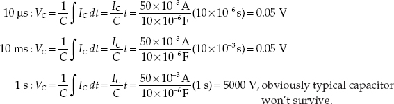
..................Content has been hidden....................
You can't read the all page of ebook, please click here login for view all page.