
Chapter 9
Discovering New Topologies
This is a journey into the world of new topologies and related techniques. It starts with a discussion of synchronous Buck and Boost topologies and shows how in complementary drive mode, they transform automatically from one to the other as the average inductor current passes through zero. Diode emulation mode is discussed along with dead time concerns and the beneficial effects of placing a Schottky diode in parallel to a synchronous FET. A detailed explanation and derivation of DCR sensing and lossless droop regulation (voltage positioning) is presented along with innovative ideas like the inductorless Buck and an unusual method of droop regulation. Next, composite topologies are discussed starting with the four-switch Buck-Boost in which an optimum drive method is proposed for ensuring glitch-free transitioning along with high efficiency. It is also revealed how the Cuk, Sepic, and Zeta are composites of the fundamental topologies. A detailed derivation of their waveforms and their RMS current and voltage stresses is included. Hysteretic topologies, including constant on- and off-time controllers, along with the active forward clamp topology are discussed in detail. Other extras include negative configurations of the basic topologies including using a Buck IC in a Buck-Boost application and vice versa.
It is always more interesting to learn a topic with the curiosity of a first-time explorer. That is the approach we will take too, as we journey deeper into switching power topologies and related techniques. We have garnered enough confidence and mastery over the fundamental topologies to move to the next stage of their (and our) evolution. However, the field being as large as it is, it is impossible to cover everything without lapsing into superficiality. Our focus here is therefore on developing the underlying intuition, hoping that will help us quickly understand much more as it comes our way in the future. Math, sometimes considered an antithesis to intuition, does help gel things together, especially at a later stage. So we have used it, albeit sparingly. But the emphasis is on intuition.
Part 1: Fixed-Frequency Synchronous Buck Topology
Using a FET (Safely) Instead of Diode
We realize that the catch diode has a significant amount of forward voltage drop, even when we are using a “low-drop” Schottky diode. Further, this forward-drop is relatively constant with respect to current. Looking at diode datasheets we see that, typically, reducing diode current by a factor of 10, only halves the voltage drop of a Schottky. Whereas we know that in a FET, the forward-drop is almost proportional to current, so typically, reducing the current by 10× reduces the voltage drop by about 10×. We can thus visualize that the presence of a diode, even a supposedly low-drop Schottky, will impair the converter’s efficiency, especially at light loads. This will also be more obvious, for almost any load, when the input is high (i.e., low D), since the diode would be conducting for most of the switching cycle, instead of the FET (switch).
We keep hearing of MOSFETs with lower and lower forward-drops (low RDS) every day, but diode technology seems to have remained relatively stagnant in this regard (perhaps limited by physics). Therefore, it is natural to ask: since both diodes and FETs are essentially semiconductor switches, why can’t we just interchange them? One obvious reason for that is diodes do not have a third (control) terminal that we can use to turn them ON or OFF at will, as required. We conclude that diodes certainly can’t replace FETs, but we should be able to replace a diode with a “synchronous FET,” provided we drive it correctly by means of its control terminal (the Gate).
What do we mean by driving it “correctly”? There are actually several flavors of “correct,” each with its pros and cons as we will see shortly. However, there is certainly an obvious way to drive this synchronous FET. It is commonly called “diode emulation mode.” Here we very simply attempt to make the FET copy basic diode behavior, but also in the process, become one with a much lower forward-drop. That means we need to drive the Gate of the synchronous FET in such a way that the FET conducts exactly when the catch diode it seeks to replace would have conducted, and stop conducting when that diode would have stopped conducting (we will likely need some fairly complex circuitry to do that, but we are not getting into detailed implementation aspects here). Conceptually at least, we presume we can’t go wrong here.
At this point, we have fast-fowarded a bit, and presented “diode emulation mode” waveforms for a synchronous Buck converter in Figure 9.1, showing the Gate drives of the two FETs and the corresponding inductor current. Note that in synchronous topologies in general, commonly used FET designators such as “upper” and “lower,” or “top”and “bottom” are not necessarily indicative of the actual function, and can always change. Therefore, in this chapter we have generally preferred to call the switch (i.e., the control FET) as “Q,” and the synchronous FET as “Qs.” That cannot change!
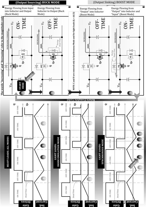
Figure 9.1: Fixed-frequency, synchronous Buck waveforms.
We note that at “high loads” (i.e., with the entire inductor current waveform above “sea-level”), the waveforms are virtually indistinguishable from the classic “non-synchronous” Buck operating in CCM (though, of course, we expect better efficiency, something not obvious looking at the waveforms). Similarly, at light loads, by applying the Gate voltage waveform for Qs as shown in the figure, we ensure the synchronous FET conducts in such a manner that the waveforms are virtually indistinguishable from a non-synchronous Buck operating in DCM. So, we ask: if these waveforms are true, does that mean we can now go ahead and remove the catch diode altogether?
Not so fast! Since we are dealing with an inductor, with almost counter-intuitive behavior on occasion, we need to be extra careful. We intuitively recognize that a catch diode is “natural” in the sense that it is available when needed — it presents a path to the freewheeling inductor current automatically, without user intervention. Basically, we can’t do anything wrong here because we are not doing anything. As mentioned in Chapter 1, the only thing we do initially is place that diode at the right place, pointing in the right direction. Then we just sit back and rely on the inductor current to set up whatever voltages are necessary to create a path to freewheel through. With all the possible permutations, we thus get our different topologies and configurations. In all cases, if the diode path is available, the inductor will not “complain” in the form of the “killer voltage spike” discussed in Figure 1.6. However, when we use a FET instead of a diode, that is, a synchronous FET, we have an additional control terminal. And with that extra authority also comes additional responsibility. For example, if this FET is somehow OFF at the wrong moment, we could conceivably resurrect the killer voltage spike. Therefore, with these sobering thoughts in mind, we now start re-examining some real-world synchronous FET scenarios with extra diligence. Our focus is based mainly on the fact that in reality, the Gate controls for Q and Qs will not be perfectly matched, and will not turn ON and OFF as precisely as we may have planned (due to driver delays, inherent latencies, process variations, and so on).
Birth of Dead Time
What if Qs turns ON a little before Q has turned OFF? That is potentially disastrous since both the FETs will be ON momentarily (overlap). Just as we were worried about a voltage spike associated with the inductor, now we should be getting equally worried about a current spike coming from the capacitor (in this case the input cap). This potentially dangerous “cross-conduction” spike of current (also called “shoot-through”) will flow from the input cap through both the FETs and return via ground. Note that in a synchronous Boost, discussed later, the shoot-through current flows from the output cap, and since that is usually a higher voltage, the spike is an even bigger problem.
Note: Can we see or measure this current spike? Well, in severe cases, accentuated by bad PCB layout (which can mimic the effects of mismatched Gate drives), cross-conduction could easily cause the FETs to blow up. In less severe (more common) cases, it may be neither obvious nor measurable. If we place the current probe at the “right place,” even the small inductance of the wire loop is usually enough to quell the cross-conduction spike, and so we may not see anything unusual. We have a current spike that we perhaps can’t ever see or measure, but its existence is undeniable in the form of an increased average current drawn from the input voltage source (measured with a DC multimeter, not a scope) and a corresponding decrease in the measured efficiency (more significant at light loads). The quiescent current “IQ” will be much higher than we had expected. Note that we are defining “quiescent current” here as the current drawn from the input supply when the converter is “idling” — that is, when its FETs are continuing to switch (at constant frequency), but the load connected to the converter happens to be zero. This is the point where the marketing guy often steps in and redefines quiescent current as an idling condition in which the load is zero, and the FETs are no longer switching (perhaps with the help of some dedicated logic pin). With that “slight change” in wording, suddenly, the above-mentioned cross-conduction loss term, along with any normal switching loss terms, is forced to zero, and therefore, the “no-load efficiency” becomes very high — on paper. To get a meaningful or realistic answer from this marketing guy, perhaps we should try asking: “What is the efficiency at 1 mA of load current?”
The solution to the cross-conduction problem is to introduce a little “dead-time” as shown in Figure 9.1. By design, this is a small intended delay, always inserted between one FET going OFF and the other coming ON. In practice, unless excessively large, dead-time just represents a safety buffer against any accidental or unintentional overlap over manufacturing process, temperature variations, diverse PCB layouts (in the case of switchers using external FETs), and so on.
CdV/dt-Induced Turn-On
Note that there is a phenomenon called CdV/dt-induced turn-on that is known to cause cross-conduction, especially in low-voltage VRM-type applications — despite sufficient dead time apparently being present. For example, in a synchronous Buck, if the top N-channel FET turns ON very suddenly, it will produce a high dV/dt on the Drain of the bottom FET. That can cause enough current to flow through the Drain-to-Gate capacitance (Cgd) of the bottom FET, which can produce a noticeable voltage bump on its Gate, perhaps enough to cause it to turn ON momentarily (but may be only a partial turn-on). This will therefore produce an unexpected FET overlap, one apparent perhaps only through an inexplicably low-efficiency reading at light loads. To avoid this scenario, we may need to do one or more of the following: (a) slow down the top FET, (b) have good PCB layout (in the case of controllers driving external FETs) to ensure that the Gate drive of the lower is held firmly down, (c) design the Gate driver of the lower FET to be “stiff,” (d) choose a bottom FET with slightly higher Gate threshold, if possible, (e) choose a bottom FET that has a low Cgd, (f) choose a bottom FET with a very small internal series Gate resistance, (g) choose a bottom FET with high Gate-to-Source capacitance (Cgs), and (h) perhaps even try to position the decoupling capacitor positioned on the input rail slightly far away from the FETs (even a few millimeters of trace inductance can help) so that despite slight overlap, at least the cross-conduction current flowing during the (voltage) overlap time gets limited by the intervening PCB trace inductances.
Counting on the Body-Diode
Dead-time not only improves efficiency by reducing chances of transistor overlap, but also impairs efficiency itself for two other reasons. But before we discuss that, a basic question arises: are we “tempting nature” by introducing this dead-time in the first place?
What if Qs turns ON a little after Q turns OFF? This is also what happens, in effect, when we introduce dead-time. We learned from Chapter 1 that any delay in providing a freewheeling path for the inductor current (i.e., after the main FET turns OFF) can prove fatal — in the form of a killer voltage spike. Admittedly, there may be some parasitic capacitance somewhere in the circuit, hopefully fortuitously present at the right place, which is able to provide a temporary path for a few nanoseconds. But that capacitor being typically very small would charge (or discharge) very quickly, and then the freewheeling inductor current would have no place to go. So, even a few nanoseconds of dead-time could prove disastrous. Luckily that scenario is not a major concern here. The reason is most FETs have an internal “body-diode” (shown in gray in Figure 9.1). So, for example, if the synchronous FET was not conducting exactly when required, as during the dead-times, the inductor current will pass through its body-diode for that tiny interval, as indicated with dashed arrows in Figure 9.1. As a result, no killer voltage spike would be seen, and we would have a switching topology that “abides by the rules of existence” presented in Chapter 1 (aka “don’t mess with the inductor”). However, to retain this advantage, and to indirectly make dead-time feasible, we need to ensure we really are using a synchronous FET with an internal body-diode. That is actually the easy part, since all discrete FETs available in the market have a body-diode inside them. However, a related question is: since a FET is a bidirectional conductor of current (when it is ON), what is the right way to “point” the FET (same question that we had posed for the catch diode)? We quickly realize that to avoid the killer voltage spike and present the body-diode to the inductor current whenever required, we need to go back somewhat to the way our old non-synchronous topology was working, and position the synchronous FET such that its body-diode points in the same direction as the catch diode it seeks to replace. This is the basic rule of all synchronous topologies that we need to keep in mind always.
Later we should observe that the body-diode of the control FET will also be called into play when we deal with “synchronous (complementary) mode drive” instead of the “diode emulation mode drive” currently under discussion. The correct way to connect the control FET is such that its body-diode is always pointing away from the inductor and toward the input source — otherwise the obvious problem would be that current will start flowing uncontrollably from the input source into the inductor, and that would clearly not qualify as a “switching topology” anymore.
Our conclusion is: we need a diode somewhere — we have been unable to replace it entirely. The last remaining question is: if the diode is present in the FET in the form of a body-diode, do we also need an external one in parallel to the FET?
Note: We mentioned above that “parasitic” capacitances can provide a temporary path for a short time. What if we actually put a physical cap at the “right place”? That actually leads to “resonant topologies.” We will not be discussing those in any detail in this book, primarily because they are usually of variable frequency and therefore rarely used commercially, and also because they require a completely new set of “rules of intuition,” which take much more time to develop, especially if you have just learned to think of squares, triangles, and trapezoids.
External (Paralleled) Schottky Diode
First of all, if we place an external diode in parallel to the body-diode, for it to do anything, the current needs to “prefer” that external diode in preference to the body-diode. So, we need the forward-drop of the external diode to be less than that of the body-diode. That is actually the easy part since the body-diode has a rather high forward-drop (more than a Schottky), typically varying from about 0.5 V for small currents to 2.5 V for much higher currents (the drop being even higher for a P-channel FET as compared to an N-channel one). An external Schottky would, in principle, seem to meet our requirement.
Note: However, to ensure that the Schottky is “preferred” in a dynamic (switching) scenario, we need to ensure the external Schottky diode is connected with very thick short traces to the Drain and Source of the FET, otherwise the inductance of the traces will be high enough to prevent current from getting diverted from the body-diode and into the Schottky as desired. The best solution is to have the Schottky integrated into the package of the FET itself, preferably on the same die, for minimizing inductances as much as possible.
Why does the Schottky diode help so much? In an actual test conducted in early 2007 at a major semiconductor manufacturer, adding a Schottky across the internal synchronous FET of a 2.7–16 V synchronous LED Boost IC on the author’s suggestion, led to an almost 10% increase in efficiency at max load. The IC was brought back to the drawing board and redesigned with an integrated Schottky across the synchronous FET (on the same die — the vendor possessed that process technology), and was finally released a few years later as the FAN5340.
The reason for the advantage posed by the Schottky is that the body-diode of a FET has another unfortunate quality besides its high forward-drop, one that we also wish to avoid. It is a “bad” diode in the sense that its PN junction absorbs a lot of minority carriers as it starts to conduct in the forward direction. Thereafter, to get it to turn OFF, all those minority carriers need to be extracted. Till that process is over, the body-diode continues to conduct and does not reverse-bias and block voltage as a good diode is expected to. In other words the “reverse recovery characteristics” of the body-diode of a FET are very poor.
So, this is what can eventually happen in synchronous switching converters without an external Schottky. During the dead-time interval between Q turning OFF and Qs turning ON (i.e., the Q→Qs crossover), we want the body-diode of Qs to conduct immediately. We therefore inject plenty of minority carriers into it (via the diode forward current). However, the full deleterious effects of that stored charge actually show up during the next dead-time interval — when Qs needs to turn OFF just before Q starts to conduct (i.e., the Qs→Q crossover). Now we discover that Qs doesn’t turn OFF quickly enough, and so a shoot-through current spike flows through Q and Qs. This unwanted reverse current ultimately does extract all the minority carriers, and the diode finally does reverse-bias. But during the rather large duration of this shoot-through, we have a significant V×I product occurring inside the body-diode, and therefore high instantaneous dissipation. The average dissipation (over the entire cycle) is almost proportional to the duration of the dead-time since the diode is just not recovering fast enough.
The only way to avoid the above reverse recovery behavior and the resulting shoot-through is to avoid even forward-biasing the body-diode, which basically means we need to bypass it completely. The way to do that is by connecting a Schottky diode across the synchronous FET, which then provides an alternative and preferred path for the current.
Whichever direction we take, we realize that we do have a diode present somewhere on our path — a body-diode or an external Schottky. Since the diode’s forward-drop is certainly higher than that of the FET it is across, the efficiency is adversely affected on that count alone (higher conduction loss). Furthermore, if it is a body-diode, then there is an additional impact on efficiency due to the reverse recovery spike (switching loss).
Eventually, reducing the dead-time should help improve efficiency on both the above-described counts. But doing so will also increase the chances of overlap, which can then adversely affect efficiency from an entirely different angle (crossover loss). In severe cases of overlap, even overall reliability will become a major concern. We are therefore essentially walking a tight-rope here. How much dead-time is necessary and optimum? Some companies have come up with proprietary “adaptive dead-time” schemes to intelligently reduce the dead-time as much as possible, usually in real-time after several cycles of sampling, to achieve just the right amount of dead-time, thus averting overlap and also maximizing the efficiency.
Synchronous (Complementary) Drive
When we look at the top section of Figure 9.1, that is, for “heavy loads,” we see that ignoring what happens during the very small dead-time, we can simply declare that Qs is ON whenever Q is OFF, and vice versa. Their drives are considered “complementary.” Therefore, design engineers just took the Gate drive as applied to Q, put an inverter to it, and applied that to the Gate of Qs (ignore dead-time circuit enhancements here). We call this a “synchronous (or complementary) mode” in contrast to the diode emulation mode discussed previously. This synchronous mode is also sometimes called the “PWM mode.” It worked as expected, just like a conventional non-synchronous topology, at least when the load was high. However, using this simple drive, as the load was lowered, the familiar-looking DCM voltage waveforms were no longer seen. In fact the well-behaved voltage waveforms normally associated with CCM remained unchanged even as the inductor current dipped below “sea-level” (zero). On closer examination, stark differences had emerged in the current waveforms. As shown in the lowermost section of Figure 9.1, two new phases had appeared, both with inductor current pointing in the “negative” direction (i.e., flowing away from the positive output, toward the input). These are marked “C” and “D.” During C, current flows in the reverse direction through Qs, whereas in D it flows in the reverse direction through Q.
This is how the system gets to C and D after B is over.
a. In B, the current flows in the “right” (conventional) direction, freewheeling through Qs and L. We know that the voltage across the inductor is reversed as compared to its polarity during the ON-time of the converter. So, during B, the inductor current ramps down. This is normal behavior so far. However, the current then reaches zero level. At that point, instead of “idling” at zero current as in DCM, since Qs is still conducting, and we know that FETs can conduct in either direction, the current does not stop there, but continues to ramp linearly down, past zero, becoming negative in the process. That is phase C. Note that in effect, we are continuing to operate in CCM since no discontinuity in current has occurred at the zero crossing level.
b. During C, the current continues to ramp linearly downward, till Qs finally turns OFF and Q turns ON. This causes the voltage across the inductor to flip once again, and with that, its polarity is now such that it causes the inductor current to ramp upward once again. This upward inflexion point, though still within the negative current region, marks the start of phase D. Note that though the current is still negative, it is now rising, commensurate with the newly applied voltage polarity. The current continues to rise linearly past zero straight into phase A (again). In A, the current is positive and continues rising, exactly as in the conventional ON-time of a non-synchronous converter. After that B starts.
The key to not getting confused above is to remember that a positive voltage across an inductor (ON-time) produces a positive dI/dt (upward ramp), whereas a negative voltage (OFF-time) causes a negative dI/dt (downward ramp). So, the inductor’s voltage polarity determines the polarity of the rate of change of current (slope dI/dt) — it has nothing to do with the actual polarity of the current itself (I), which can be positive or negative as we have seen above.
What are the main advantages of “synchronous mode”? We get constant frequency, no ringing during the idling time (and therefore more predictable EMI), easier Gate drive circuitry, constant duty cycle (even at light loads), simpler stress (RMS) equations to compute (see Chapter 19). The key advantages of “diode emulation mode” are reduced switching losses (there are no turn-on crossover losses since the instantaneous current is zero at the moment of crossover) and generally more stable though admittedly sluggish response (single-pole open-loop gain; no low-frequency right-half-plane zero, no subharmonic instability).
Part 2: Fixed-Frequency Synchronous Boost Topology
Energy in an inductor is ½LI2. Its minimum value is zero, and that occurs at I=0. On either side of I=0, inductor energy increases. Stored energy doesn’t depend on the direction (polarity or sign) of the inductor current. In fact, generally speaking, assigning a positive sign or a negative sign to current is an arbitrary and relative act — we only do it to distinguish one direction from the other, the sign by itself has no physical significance. With this in mind, we look a little more closely at the lowermost section of Figure 9.1. In terms of energy, during A, we are first pulling in energy from the input and building up energy in the inductor. Then, during B, the stored energy/current freewheels into the output. This is conventional operation so far. But after that, things change dramatically. Judging by the new direction of current shown in C, we now start pulling in energy from the output, but nevertheless still building up energy in the inductor. Finally, in D, that energy/current freewheels into the input cap. We ask: isn’t that a Boost converter by definition? We are momentarily taking energy from what is the lower-voltage rail, and pumping energy into the higher-voltage rail. We realize that now there is a Boost mode occurring in our “Buck converter.” Finally, after D, we start the cycle once again at A and deliver energy from the higher to the lower rail again just as a conventional Buck converter is expected to do.
We realize that the synchronous Buck operating at light loads always functions as a Boost for a brief part of its switching cycle. So we can well ask: why is the schematic in Figure 9.1 still called a “Buck,” not a Boost? In fact, the schematic is the same for both the Buck and the Boost topologies as we will shortly see, the difference being purely functional. In Figure 9.1, the topology is a “Buck,” not a “Boost,” only because the Buck side is “winning” overall, as per the current waveforms sketched. This means that the center (average) of the inductor current waveform is shown above “sea-level” (positive), implying that net energy/current is flowing in a direction from left (higher-voltage rail) to right (lower-voltage rail). However, if the center of the inductor current waveform was below sea-level, that would imply there is a net flow of current/energy from right (lower rail) to left (higher rail). We would then have a synchronous Boost converter on our hands, rather than a Buck converter (though admittedly, to sustain the flow in that direction, we need a proper voltage source on the right side, instead of just a resistor and capacitor). This subtle topology transformation occurs as the average inductor current moves across the zero current boundary. That is shown more clearly in Figure 9.2.
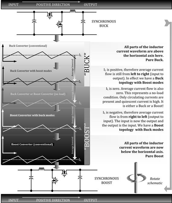
Figure 9.2: As the average inductor current is lowered below zero, a synchronous Buck becomes a synchronous Boost.
To summarize: with reference to Figure 9.1, as the inductor current dips below sea-level, we get a Boost converter, but initially one which is operating as a Buck for a brief part of its switching cycle — just as above sea-level, we previously had a Buck converter, but one which was operating as a Boost for a brief part of its switching cycle. However, it remains a “Boost converter” because the Boost modes of its operation are “winning” as compared to its Buck modes — reflected in the fact that the average inductor current is negative, that is, from right to left. But as the average current dips further below, till finally no part of the inductor current waveform remains above sea-level, we get a full conventional Boost converter operating in conventional CCM, one which is not even momentarily operating as a Buck.
We thus realize that when we use synchronous (complementary) drives, the conventional DCM mode for both the synchronous Buck and the synchronous Boost topologies gets replaced with a new CCM-type mode in which a good amount of energy is simply being cycled back and forth every cycle, even though very little energy (maybe zero) is actually flowing from the input into the load. This recirculating energy does not promise high efficiency (“much ado about nothing”), and that is one reason the synchronous (complementary) drive mode is not used in cases where battery power, for example, needs to be conserved — in that case diode emulation mode with enhancements like pulse-skipping is more commonly used.
What happens to crossover losses? It is often stated that in a switching topology, the control FET has crossover losses, but not the synchronous FET (or catch diode). That is a fairly accurate statement generally. However, we can now visualize that when a Buck converter is operating in Boost mode (negative current), in those Boost parts of its cycle we have switching losses in Qs, not in Q.
A little bit about the difference in “schematics” versus “functionality.” We perhaps viewed the schematic in Figure 9.1 rather instinctively from the left side of the page to the right. We are intuitively most comfortable with schematics which are drawn “left-in, top-high,” that is, where the input source is on the left side of the page and the higher-voltage rail is placed on the top. But suppose now we look at the same schematic of Figure 9.1, from the right side to the left. Isn’t that exactly how we would draw a synchronous Boost topology (based on what we have learned)? Alternatively, if we mirror the Buck schematic of Figure 9.1 horizontally, it will become a Boost schematic. However, functionally speaking, to make any difference in behavior, we have to actually change the polarity of the average inductor current (above or below sea-level in our example). Only then does a given schematic work as a Buck or a Boost converter, irrespective of what it may look like to us. In other words, in dealing with synchronous topologies, because they can source or sink current equally readily, we have to be really cautious in jumping to any conclusion about the underlying topology simply based on the way the schematic looks. The key is looking at the average inductor current level (center of ramp) — its actual functioning.
In Figure 9.1, the “negative” current of a Buck would be considered a “positive” current for a Boost. In other words, regions C and D in Figure 9.1 would be conventional (positive current) operation if we had a Boost converter on hand. And then, A and B would be regions of negative Boost inductor current. To make things clearer, we have carried out a full mirror reflection in Figure 9.3 to see how a synchronous Buck schematic gets transformed effortlessly into a synchronous Boost schematic. We observe that (for the case of complementary drives) the voltage waveforms are completely unchanged from what they were in Figure 9.1. The current waveform, however, is not just a mirror reflection, but is also vertically shifted so as to change its average value (and polarity) as explained above. Only then, functionally speaking, do we get a Boost converter, not a Buck converter.
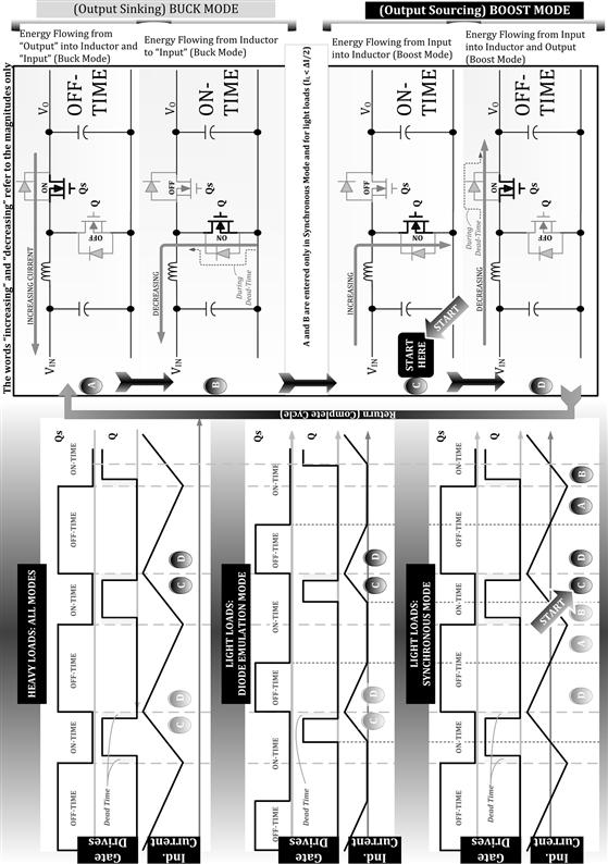
Figure 9.3: Fixed frequency, synchronous Boost waveforms.
With this insight, we can perhaps examine more formally how exactly a Buck maps into a Boost. We realize that if the average inductor current in Figure 9.1 dipped below sea-level and the synchronous Buck became a synchronous Boost, there would be no difference in the ensuing voltage waveforms. However, when we get a Boost, energy would be building up in the inductor (albeit with reverse current flow) during what was originally the “OFF-time” for the Buck. That interval therefore is now officially the “ON-time” for the Boost. So, in effect, TON has become TOFF, and TOFF is now TON, which means D has become 1−D. And also, “output” has become the “input,” and vice versa. With this mapping we get
![]()
Simplifying, we get
![]()
No surprise: this is the familiar equation for the DC transfer function of a Boost topology. We now realize, that based on our new level of intuitive understanding, the Buck and Boost are just mapped versions of one to the other — with the key change being INPUT ↔ OUTPUT. No wonder, in a Buck, we say that the average input current equals the average current through the upper transistor (or the “switch” in non-synchronous versions), whereas in a Boost we say that the average output current equals the average current through the upper transistor (or the “catch diode” in non-synchronous versions). Also, in a Buck, the average inductor current equals the average output current, whereas in a Boost, the average inductor current equals the average input current. And so on. The resemblance is quite startling actually.
But to be clear: the Buck and Boost are still independent topologies — they just happen to be mirror images of each other under certain conditions. We speculate: is this like the electron and the anti-electron? We recall these are considered different particles, but are also “mapped” versions of each other. Similarly for a male and a female — similar, yet different, if not opposite. It therefore seems natural to ask: what happens if we put the Buck and Boost together back to back? What do we get? In fact, we get the “four-switch Buck-Boost,” as described further. Later we will also generate several Boost-Buck composites. But before we discuss all that, some essential housekeeping is required. Here are some practical hints to start with:
a. A Buck can under severe transient conditions become a Boost for several cycles. If the output voltage is lower than its reference, it tries to get up to the reference level by turning its control FET ON. But if the output voltage is higher than its reference (as during a sudden unloading of the output), it tries to actively discharge the output cap, that is, it becomes a Boost converter. Therefore, while evaluating a Buck, we should put a voltage probe on its input cap too, especially in low-voltage applications where even a slight bump in input voltage may cause the voltage ratings of the FET to be exceeded.
b. Sometimes we start up a Buck converter into a “pre-charged” or “pre-biased” load. For example, we may have simply turned OFF the Buck momentarily, leaving its output cap still charged (connected to a zero/light load), and then tried to turn the converter back ON rather too quickly — only to find the output was still high. In many designs, Buck controllers use a “soft-start” sequence while turning ON. In many of those design implementations, the reference voltage (as applied to the error amplifier) is slowly raised from a very low level up to the normal level. In such cases, a pre-biased load will appear as an overvoltage initially. The error amplifier will therefore reduce its duty cycle sharply in response. However, if we have a complementary drive, then the OFF-time of the Buck is correspondingly very large now. So now the lower transistor may be ON for a very long time. Since the OFF-time of a Buck maps into an ON-time for a Boost, in effect, we once again have a fully functioning Boost converter operating for quite some time. The pre-biased load is now serving as the input voltage source to this reverse converter. The energy being pulled in from the pre-biased load eventually goes into the input cap of the Buck. If that cap is small, and if the input voltage source (on the left) is not “stiff” enough, the cap can easily get overcharged, causing damage to the Buck controller.
c. We may therefore need to significantly oversize the input bulk capacitance, well beyond its rating based on RMS current, or an acceptable input voltage ripple, just to keep this “Boost bump” down.
d. Another concern is that when the circuit is functioning as a Boost, we need to limit the current in the lower transistor too, otherwise when the lower transistor turns ON (sometimes fully for a while), we will have absolutely no control over the current being pulled out of the pre-biased load, and that may damage the lower FET especially since the inductor also likely saturates in the bargain. Therefore, we may need to incorporate current limits on both the high- and low-side FETs of the synchronous Buck/Boost.
e. One way of handling pre-biased loads better is to not operate with complementary drives during soft-start, but power-up in diode emulation mode. Or, the duty cycles of both the upper and the lower FETs should be increased gradually with appropriate relative phase, moving smoothly from soft-start mode to full complementary mode without any output glitch or discontinuity. Quite a few proprietary techniques abound for this purpose.
f. One way of indirect current limiting, located in neither of the FETs, is called “DCR (DC resistance) sensing.” This can be applied to any topology actually. It is discussed in the next section.
Part 3: Current-Sensing Categories and General Techniques
In general, current sensing/limiting has several purposes and implementations. We need to know what the basic aim is before we decide on an implementation technique. There are several possibilities to choose from here.
a. Cycle-by-cycle current limiting: This is used for switch protective purposes. There are situations, especially in “high-voltage” applications (defined here as anything applied above 40–50 V on an inductor/transformer), where even one cycle of excess current can cause the associated magnetic component (inductor/transformer) to saturate sharply, leading to a very steep current spike that can damage the FETs. So, we are often interested in providing a basic, but very fast-acting current limit, threshold which if breached, will cause the FET to turn off almost immediately — well within the ongoing ON-time of the cycle. Note that any delay in limiting the overcurrent, even for 100–200 ns, can be disastrous, as shown in Figure 2.7.
b. Average current limiting: This is also for protective purposes, but is more relaxed than (a), since it spans several cycles. It is often used in low-voltage applications because in such cases, the magnetic components usually don’t see high-enough applied voltseconds to saturate too “sharply,” that is, their rate of increase of B-field with respect to the applied Ampere-turns is quite small. And even if the magnetics do start to saturate somewhat, the typical circuit parasitics present on the board help significantly in curtailing any severe resulting current spikes. So, generally speaking, we can tolerate a few cycles of overload current without damage. Average current limiting is then considered adequate, but it is still recommended to have at least some duty cycle limiting to assist it. For example, 100% duty cycle (i.e., the switch turned ON permanently for several cycles, as in some Buck converter architectures) can be disastrous with only average current limiting present.
In AC–DC converters, there is cycle-by-cycle current limiting already present on the main switching FET. That makes the transformer relatively safe from saturation. In such cases, the purpose of providing additional average current limiting on the secondary outputs is primarily to comply with the international safety norm IEC-60950. This norm requires that most safe, nonhazardous outputs be limited to less than 240 W within 60 s. Therefore, we actually want a slower current limiting technique in such cases, to avoid responding too aggressively or restrictively to overloads, since those temporary overloads may just represent normal operation. In brief, average current limiting is generally geared toward providing protection against sustained overloads, certainly not against the rapid effects of core saturation. Therefore, RC filtering with a rather large time constant is used to filter the current waveform. We then apply that time-averaged level to the input of a current-limit comparator, and compare that to a set reference threshold applied on the other input pin of the comparator.
c. Full current sensing: This can be used for both control and protection. The difference as compared to (a) and (b) is that in those cases we only wanted to know when the current crossed a certain set threshold (and whether slowly or quickly). But we were certainly not interested in knowing the actual shape of the current waveform while that happened. However, in many other cases, we may want to know just that. In fact, we need to know the entire current waveshape (AC and DC levels) when using current-mode control, for example — in which method the sensed current waveform provides the ramp applied to the PWM comparator.
How can we implement the above current-sensing strategies? The most obvious way to implement any form of current sensing (monitoring), or limiting, is to insert a current-sense resistor and monitor the voltage across it. But that is obviously a lossy technique since we dissipate I2R Watts in the resistor. Note that any attempt to lower the dissipation by reducing R is not very successful beyond a certain point because switching noise starts to ride on top of the relatively small sensed signal, drowning it out eventually. We can try to filter out the noise by introducing a small RC filter on the sensed current waveform, but we usually end up distorting the sensed signal and introducing delays. Some engineers try to avoid the I2R loss altogether by sensing the forward voltage drop across the FET — since that is essentially a resistance called “RDS.” We do, however, need to compensate that sensed voltage for the well-known temperature variation of RDS (the factor depends on the voltage rating of the FET). We thus realize that this FET-sensing technique can work only when the FET itself is completely identifiable in terms of its characteristics, and also we are able to monitor its temperature. This indirectly demands the FET be integrated on the controller die itself — that is, with FET-sensing technique, we should use a switcher IC, not a controller with external FETs. But there is another possible problem in using the FET-sensing technique. Nowadays, there are situations where we might not even turn-on the lower or the upper FET for several cycles (e.g. pulse skipping mode). We realize that to sense current through a FET, we have to at least turn it ON. Therefore, another attractive set of techniques has evolved for implementing “lossless” sensing. One such popular method is called DCR Sensing.
DCR Sensing
Perhaps it all started with this simple thought: instead of putting a sense resistor in series with the FET, why not put the sense resistor in series with the inductor? We would then obtain full information about the inductor current, rather than just the ON-time or OFF-time slice of it. This could conceivably help us in implementing various new control and protection techniques too. However, that thought process then went a step further by asking: since every inductor has a resistance “built-in” already, called its DCR, could we somehow use that resistance in place of a separate sense resistor? We would then have “lossless current sensing,” since we are at least not introducing any additional loss term into the circuit. The obvious problem here is that the DCR is itself inaccessible: we just can’t put an error amplifier or multimeter “directly across DCR” because DCR lies buried deep within the object we call an “inductor.” However, we want to persist. We ask: is there some way to extract the voltage drop across this DCR from out of the total inductor voltage waveform? The answer is, yes, we can — and that technique is called DCR sensing.
To start with, in Figure 9.4 we present an unusual, but an original and innovative, method to provide basic average current limiting. Though it is not very accurate, it has been used very successfully in very large production volumes on the output of a commercial 70-W AC/DC flyback (for meeting safety approvals). Note that it uses a filter with a very large RC time constant.
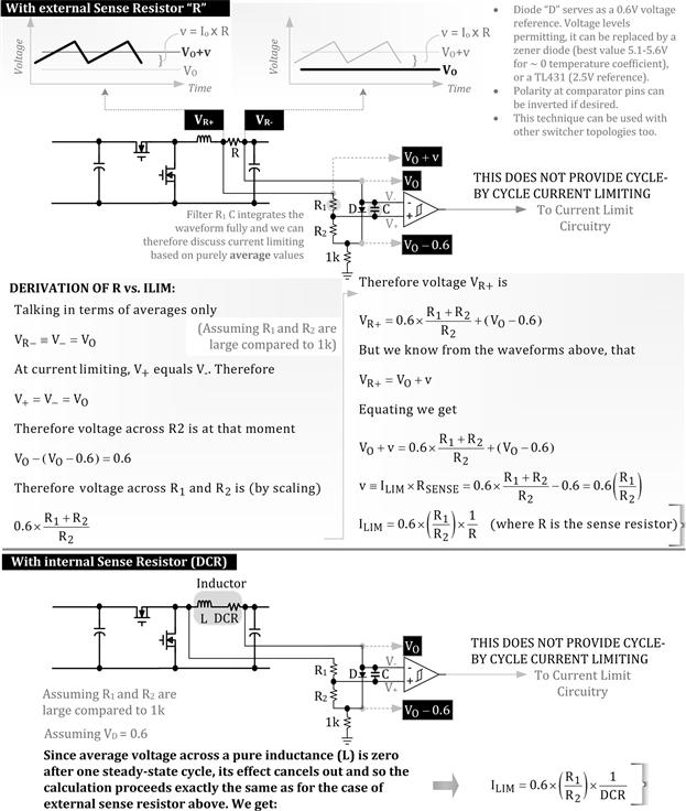
Figure 9.4: A DCR-based average current-limiting technique.
The top part of the figure shows how we can implement this current-sense technique with a discrete (external) sense resistor in series with the inductor. In the lower part of the figure, we indicate that this technique will work just fine using the DCR of a Buck inductor too. Why is that? Because, if we have a pure inductor (no DCR) and we average its voltage over a cycle, we will get exactly zero — because in steady state, an inductor has equal and opposite voltseconds during the on-time and off-time — by the very definition of steady state! When we use a real-world inductor, with a certain non-zero DCR, the additional drop during both the ON-time and the OFF-time is IO×DCR, and that is clearly the term which remains after we average the inductor voltage over one complete cycle or several cycles. That is the DC voltage being applied on the comparator pin in Figure 9.4.
Just for interest, we note that in the 70-W flyback we mentioned above, the “sense resistor” used was the small resistance of the small L (rod inductor) of the LC post filter of the flyback.
Note that this DCR sensing technique uses a very large RC time constant, and so we lose all information about the actual shape of the inductor waveform. That doesn’t matter however, because in this particular case, we just want to implement average current limiting. But we now ask: can we extend the same technique to full current sensing?
In Figure 9.5, we present how this is done rather commonly nowadays. In this case, the RC time constant is not large, but it is in fact matched exactly to the time constant of the L–DCR combination, which means mathematically: RC=L/DCR. We see from the Mathcad graphs embedded in the figure that with this matching, and stated initial conditions, the voltage on the capacitor becomes an exact replica of the voltage across the DCR. Further, for any duty cycle other than the steady-state duty cycle, the manner in which the DCR voltage (and therefore inductor current) changes is also replicated exactly by the capacitor voltage, which means that the two voltages indicated will track each other accurately under all conditions, steady state or otherwise. For example, if the inductor current is momentarily unsteady (as during a line or load transient), the capacitor voltage will not be steady either. But it is interesting that in fact, both the DCR voltage and the cap voltage will increase or decrease by exactly the same amount from this point on. This indicates that both the voltages will change identically (i.e., track each other), and finally settle down identically too, at their common shared steady-state initial voltage condition. Note that the settling/initial value, as indicated in the figure, is IO×DCR.
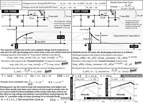
Figure 9.5: DCR current sensing explained (with exaggerated DCR).
The advantage of the above fancy version of DCR sensing is that the entire AC and DC information of the inductor current waveform is now available via the sensed capacitor voltage (assuming, however, that the inductor does not saturate somewhere in the process).
Is there any simple intuitive math to explain this time-constant matching and the resulting tracking? Yes, but it is not a rigorous proof, as we will see. Let us start by applying the duality principle. We know that the voltage on a capacitor when charged by a current source is similar to the current through an inductor when “charged” by a voltage source. Assuming steady-state conditions are in effect, and also that the maximum voltage on the capacitor is low compared to the applied on-time and off-time voltages (VON and VOFF, roughly VIN–VO and VO respectively), we get near constant-current sources (VON/R and VOFF/R) charging and discharging the cap during the ON-time and OFF-time, respectively. The question is: what is the cap voltage swing during the ON-time and during the OFF-time. Further, are the swings identical in magnitude, or is there a “leftover delta” remaining at the end of the cycle, indicative of a nonsteady state?
Using
![]()
![]()
We know from the voltseconds law that
![]()
Therefore,
![]()
Similarly, for the inductor current, using
![]()
we get
![]()
We know from the voltseconds law that
![]()
Therefore,
![]()
We conclude that there is no leftover delta remaining at the end of the cycle for either the inductor current swing or the cap voltage swing. Therefore, both inductor current and cap voltage are in steady state. That is just duality at work (as introduced in Chapter 1).
Let us now compare the capacitor voltage swing and the DCR voltage swing and try to set them equal, so we can get them to be exact copies, rather than merely scaled copies, of each other.
Set
![]()
equal to
![]()
Therefore,
![]()
Or
![]()
That is the basic matched time-constant condition for DCR sensing, and we see it follows rather naturally from the simplified intuitive discussion above.
This simple analysis does indicate that the cap voltage is mimicing the inductor current. It tells us quite clearly that the AC portion of the inductor current is certainly being copied by the cap voltage. But what can we say about the DC level? Is the DC cap voltage copying the DC inductor current too? It actually does, but that does not follow from the simple intuitive analysis presented above (or from any complicated s-plane AC analysis you might see in literature). For that we should look at Figure 9.5.
Note that in Figure 9.5, we have used the accurate form of voltages appearing on the capacitor during the ON-time and OFF-time. Those include the small (but decisive) term IO×DCR, which eventually determines the DC value of the capacitor voltage. The DC value is easy to understand based on the analysis we presented earlier when discussing Figure 9.4. We recall that after we average out the voltseconds, the IO×DCR term is all we are left with. So clearly, that must be the DC value of the capacitor voltage waveform in the present case too. Philosophically, we recognize that time constants don’t enter the picture when performing DC analysis. The effects of time constants are time bound by definition. So we conclude that both Figures 9.4 and 9.5 must provide the same DC/settling values ultimately.
We realize that with good time-constant matching, the DCR voltage in Figure 9.5 becomes a carbon copy of the capacitor voltage, and vice versa — with both AC and DC values replicated. We ask: is that replication true only in steady conditions or is it also true under transient conditions? We see from Figure 9.5, for the cases of duty cycle other than steady state (i.e., n not equal to 1), that the change in cap voltage is also an exact replica of the change in DCR voltage (referring to the leftover delta at the end of the cycle). That means both the cap voltage and the DCR voltage (corresponding to inductor current) will climb or fall identically under transients, heading eventually toward their (identical) steady-state values. This implies that their relative tracking is always very good, steady state, or otherwise.
However, in reality, DCR sensing is not considered very accurate and should not be relied upon for critical applications. For example, it is well known that the nominal DCR value has a wide spread in production, and the DCR itself varies significantly with temperature. So, the last remaining question is: what are the effects of mismatched time constants (L/DCR and RC)? We have seen that the inductor current reaches steady state based on an initial (DC) condition I=IO, and corresponding to that, the capacitor voltage reaches steady state with an initial (DC) condition of v=IO×DCR. We expect that to remain true for any time constant, since after several cycles, the effect of any time constant literally “fades away.” In other words, the DC value of the cap voltage waveform cannot vary on account of mismatched time constants per se (but will obviously change if DCR itself varies). When subjected to a sudden line or load transients, the effect of mismatched time constants will be severe (though only temporarily so). For example, if the capacitance of the RC is very large, the cap voltage will change very little and rather slowly, as compared to the inductor current. But final settling value will be unchanged (for same DCR).
Note that many commercial ICs allow the user to either choose the DCR for cost and efficiency reasons, or use an external sense resistor (in series with the inductor) for higher accuracy.
The Inductorless Buck Cell
The power of “what-if” can be uniquely powerful in power conversion. So, as a variation of classic DCR Sensing, we ask: what if we reposition the lower terminal of the capacitor in Figure 9.5 and connect it to ground, as shown in Figure 9.6?
Figure 9.6: Inductorless Buck and an alternative regulation and current-sensing scheme (shown with exaggerated DCR).
For negligible DCR, we will discover that (for fairly large capacitances) the capacitor voltage will be the same as the voltage on the output capacitor of the Buck converter. That is interesting. But we also notice that by repositioning the cap, the series RC no longer rides on the output rail, but is separate from the LC. The two branches, RC and LC, are independent and in parallel now. This implies we can
a. disconnect the LC branch completely. In other words, we can just toggle the FETs at a certain predetermined duty cycle D and the result (i.e., the cap voltage of the RC) will be a (low-power) output rail of voltage VO=D×VIN — same as for the classic Buck converter. Or we can introduce an active feedback loop too. We now have an “inductorless Buck cell” (named by the author and first published in EDN magazine on October 17, 2002). Note that this is a variation of the bucket regulators we presented in Figure 1.2. Here, by changing the duty cycle, we can use this circuit to generate any output rail, perhaps as a reference voltage. We can’t really use it to give out much power, and neither is it efficient. But it can be quite useful as we will see.
b. also decide to retain the LC (inductor and the output capacitor of the Buck), but shift the regulation point from the output capacitor of the Buck to the capacitor of the series RC. Especially under large-signal conditions, we expect the RC-based feedback loop to have better behavior than a corresponding double-pole LC-based feedback loop.
For non-negligible DCR, we find that
c. with the same time-constant matching as we used in DCR sensing, the cap voltage minus the output rail is equal to the DCR voltage. So, we get back the DCR sensing we had in Figure 9.5, but now in addition, we can also implement a new well-behaved feedback loop. Both are shown in Figure 9.6. These signals can be jointly used for current-mode control.
d. we can also achieve “lossless droop regulation” as discussed next.
Note that this inductorless Buck technique can also be used in non-synchronous converters. But in that case we always need to have the LC present in parallel to the RC. Because in the absence of a synchronous FET actively forcing the switching node (close) to ground during the OFF-time, the current flowing in L becomes responsible for accomplishing that. We have to get voltage applied to the RC to actively toggle repetitively. Otherwise the cap of the RC would just charge up to the input voltage.
Lossless Droop Regulation and Dynamic Voltage Positioning
In Figure 9.7, we start with a conventional Buck. Then we move down to the next schematic and introduce a droop resistor “Rdroop.” This is one of the conventional ways of implementing droop regulation. Note that we are now regulating the point marked VO+(IO×Rdroop) instead of regulating VO, which means that VO is no longer fixed. Because, for example, if the current IO rises, VO+IO×Rdroop will tend to increase. But since we are holding VO+IO×Rdroop constant by means of the regulation loop, the only solution is for VO to decrease as IO increases. This is called droop regulation or “dynamic voltage positioning.”
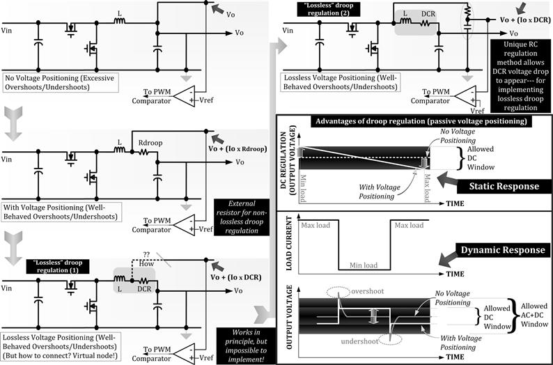
Figure 9.7: Conventional voltage positioning (droop regulation) and a novel lossless inductorless Buck implementation.
Now, we would like to do this with DCR instead of Rdroop, since that would be considered lossless. But DCR is not accessible. However, from Figure 9.6 we have learned that the inductorless Buck cell provides a rail that is exactly equal to VO+(IO×DCR). Further, the good news is that this point is accessible. So, if we connect the error amplifier to it, we will achieve the same basic effect as conventional droop regulation (proposed by the author here).
What are the benefits of droop regulation in general? In Figure 9.7, we show the transient response waveforms with and without droop. The advantage of droop is very simply explained as follows:
a. Unload: At high loads, the output voltage with droop is lower than without droop. This gives us additional headroom literally. So, if we suddenly unload the output, the output will jump up momentarily (its natural transient response). But since the output rail of the converter with droop implemented starts at a lower level, the highest voltage it goes up to under transient conditions is also lower. So, with good all-round design, we can ensure the highest point does not exceed the permissible AC+DC window, and also that the voltage finally settles down close to the upper end of the allowed DC window.
b. Load: Now, if we suddenly apply max load, the output will tend to momentarily go much lower (its natural transient response). However, with droop implemented, the output starts off at a higher level than the output of a converter without droop. So, the lowest point will now be higher, and we have a better chance of avoiding undershoot.
We see that droop regulation naturally “positions” the output at a “better level” to start the excursion with, so it is more suited to avoiding overshoots and undershoots. This is very useful especially in VRM-type applications, where the allowable regulation window is, indeed, very tight.
Part 4: The Four-Switch Buck-Boost
We had mentioned previously that the Boost and Buck are horizontally reflected and mapped versions of each other and that it would be interesting to see what happens if we place them back to back, like an electron with an anti-electron.
In the top schematic of Figure 9.8, we started with a Buck converter positioned at the input and follow it up with a Boost converter. However, we then realize that neither the output capacitor of a Buck nor the input capacitor of a Boost is fundamental to their respective topologies, since in both cases there is an inductor in series, and the only purpose of these capacitors is to filter out the relatively small ripple of the inductor. So, in the middle schematic of Figure 9.8, we meld the two converters together to produce our first composite topology: the “four-switch Buck-Boost.” We can continue to view it mentally as a cascade of a Buck cell followed by a Boost cell. The cell consists of a totem-pole of two FETs driven in complementary fashion. We can visualize that the Buck stage has an output (a virtual one in this case) called “Vx,” which becomes the input rail to the Boost cell. So the DC transfer function of the composite can be broken up into a product of its cascaded consitutents as follows:
![]()
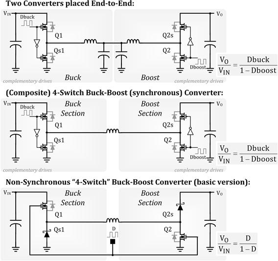
Figure 9.8: Evolution of the general four-switch Buck-Boost and its simpler lower-efficiency non-synchronous version.
In the lowermost schematic of Figure 9.8, we tie the Gates of the control FETs of both the Buck and the Boost sections together. So, Dbuck=Dboost=D. In that case,
![]()
which is the same DC transfer function as for the classic single-transistor (or its two-transistor synchronous version) Buck-Boost topology.
The biggest underlying advantage of this composite topology is that unlike the fundamental single-switch, single-inductor Buck-Boost, the polarity of the output is not inverted with respect to the input.
We discuss two distinct categories of control here.
a. Single duty cycle: The non-synchronous version of this was presented in the lowermost schematic of Figure 9.8. We show its synchronous version in Figure 9.9. The common feature of both is that there is only a single duty cycle D applied, and the DC transfer function is D/(1−D). There are advantages and disadvantages to this simple control approach. Briefly:
Advantages: Simplest drive possible; seamless step-up/step-down operation (centered around D=50% for the case VO=VIN as for classic Buck-Boost topology); and no polarity inversion from input to output.
Disadvantages: Higher conduction losses (two semiconductor switch drops during both ON-time and OFF-time); higher switching losses (both totem-poles constantly switching, e.g., no LDO-type pass-through mode when VO≈VIN); both input and output caps always have high RMS currents; and overall poor efficiency (60–70%).
b. Dual duty cycle: As presented in the middle schematic of Figure 9.8 and further elucidated in Figure 9.10, the two totem-poles, though synchronized to the same clock, have two distinct duty cycles: “Dbuck,” applied to the Buck totem-pole cell and “Dboost,” applied to the Boost totem-pole. Though in all implementations, the DC transfer function is Dbuck/(1−Dboost), there are many flavors of this approach as we will shortly see. Broadly speaking, the advantages and disadvantages of this approach are as follows:
Advantages: No polarity inversion from input to output and lower switching losses (both totem-poles are not constantly switching).
Disadvantages: Complex Gate drives; many patents in force; higher conduction losses (two semiconductor switch drops during both ON-time and OFF-time); input or output (or both) caps can have high RMS currents; nonseamless step-up/step-down operation (mode transitions occur around duty cycles limits of 0% and 100%); and potential lack of proper “retraceability” (i.e., going from VIN>VO to VIN<VO and back to VIN>VO may involve different duty cycle combinations in either direction, and therefore varying efficiency paths).
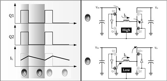
Figure 9.9: The simplest, lowest efficiency synchronous version of the general four-switch Buck-Boost.
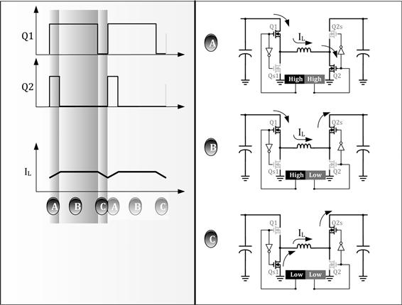
Figure 9.10: One possible implementation of the four-switch Buck-Boost in the region VIN≈VO.
Note: In all discussions involving the four-switch Buck-Boost, we are focusing only on the case of fully complementary drives (no diode emulation mode). Therefore, in either the Buck or the Boost totem-poles, when one transistor of a given totem-pole is ON, the other is OFF, and vice versa. We have consequently just drawn the Gate waveforms for the control FETs Qx in the related figures and consciously omitted the Gate waveforms of the synchronous FETs Qsx. Further, for simplicity, we are assuming that the average inductor current never intersects the zero current axis (i.e., there are no recirculating energy modes as discussed in Figures 9.1–9.3).
One of the key advantages of independent Buck- and Boost- section duty cycles is that if for example, overall, step-down performance is required, say from 5 V to 3.3 V, then there is no need to ever toggle the Gates of the Boost section. We can just toggle the Buck section with duty cycle Dbuck=VO/VIN, and keep the Boost section in pass-through mode, that is, with Dboost=0. So, current from the inductor will simply pass straight through the upper FET of the Boost section into the output. Similarly, if step-up performance is required, say from 3.3 V to 5 V, there is no need to toggle the Gates of the Buck section. We can just toggle the Boost section with duty cycle Dboost=1−(VIN/VO), and keep the Buck section in pass-through mode, that is, with Dbuck=100%. So, current from the input will pass straight through the upper FET of the Buck section into the inductor. By doing this, we save on switching losses across most of the regions of operation. All known implementations of the four-switch Buck-Boost (with dual duty cycle) agree on this aspect — there is no difference in most of the known implementations in the regions where VO is different from VIN. Any differences in approach are located within the region VIN≈VO, for example, 5 V (nominal) to 5 V (exact) conversion. Note that on either side of this region we actually also have two FET forward-drops to account for. So, this particular region, designated “VIN≈VO,” can in reality be a fairly wide region. In addition, max or min duty cycle limits can affect its boundaries significantly. Further, the system may spend significant operating time in this region, so high efficiency is very desirable here. Unfortunately, this is the region where both the Buck section and the Boost section are asked to toggle (switch), and therefore, switching losses are high. In addition, as we suddenly start toggling the Gates of a previously inactive totem-pole (i.e., in pass-through mode), or stop toggling the Gates of a previously toggling (switching) totem-pole, we are liable to introduce significant output glitches, besides a potential lack of retraceability.
We now look closely in Figure 9.10 at the “special region” in which both the Buck and the Boost totem-poles are being switched. We can see that on either side of this region we are in pass-through mode, either in the Buck cell or in the Boost cell. In the figure, we also recognize that at a practical level, we can usually neither achieve, nor do we actually desire, duty cycles too close to 0% or 100%. So we have set a Dmin of 0.1 and a Dmax of 0.9 for both converter stages.
Note: For example, if we are using N-channel high-side FETs in a Buck, we can’t go up to 100% duty cycle because we need to turn OFF the control FET momentarily, to allow the bootstrap circuitry to deliver charge into the bootstrap capacitor, which then provides power to the Gate driver. For a Boost (or a Buck-Boost) converter, it is never a good idea to use 100% duty cycle, since that leaves no time for the inductor to freewheel its stored energy into the output, besides possibly creating a sustained short across the input. A 0% duty cycle is almost impossible to achieve in general, since it takes a short duration to first turn ON the FET, then some time to turn it OFF. There are always some delays at each step, as the turn-on or turn-off commands are propagated and executed. Besides, there may be leading edge blanking in current-mode control which virtually guarantees a minimum ON-time. A minimum ON-time is also required in general, if we want to sense the current passing through any FET. And so on.
Note: If we are using N-channel FETs (that is, high-side FETs), we have a problem even in pass-through mode in keeping the bootstrap rail alive. We may need to include a separate standby low-power charge-pump circuit constantly switching away. Or with low-threshold-voltage FETs, we could route power to the high-side driver of the pass-through stage from the bootstrap rail of the other (switching) stage, since in all cases, the pass-through stage is the one connected to the lower of the two rails VIN and VO.
The fundamental question is: how do we control two duty cycles (in the special region)? We cannot have two control loops, one for the Buck section and one for the Boost section, since they would likely end up fighting each other. For example, if the input is close to 5 V, and the output is 5 V, we could have a case where the intermediate voltage Vx=2.5 V. The Buck would then operate at around 50% (5–2.5 V), and the Boost would also switch at around 50% (2.5–5 V). Note that this particular duty cycle combination bears strong resemblance to the simple schematic of Figure 9.9 (but only in this region). But in addition, we actually have infinite possibilities here. For example, we could also have the Buck switching at only about 80% duty cycle (intermediate voltage Vx=0.8×5=4 V), followed by the Boost switching at about 25% duty cycle (stepping up the intermediate voltage of 4–5 V). In other words, there are many ways to go even from~5 V to 5 V. Two independent control loops will never be able to decide among themselves what the best way is. Summing up: we need to have only one control loop. But there are two possibilities for that too: we can either fix one of the two duty cycles (Dbuck=constant or Dboost=constant) and then allow the control loop to vary the other. Or, we need to define a certain fixed relationship between Dbuck and Dboost so that when the control loop determines one of them, the other gets automatically defined. It can be shown that perhaps the most optimum method of driving the Buck and Boost sections in this region, one that guarantees highest efficiency and also full retraceability, is the “constant difference duty cycle method” (US Patent number 7,804,283, inventor Maniktala and Krellner). Its operation is illustrated in Figure 9.11. This is what happens as input voltage is lowered:
a. Full Buck mode initially. Dboost=0. Dbuck increases gradually as input is lowered, till Dbuck hits 90% duty cycle limit (Dmax). The control loop is in effect controlling and determining Dbuck.
b. At this point, we transit into the special region from the right side, and Dboost, previously in pass-through mode, is now forcibly increased from 0% to 10%.
c. The control loop responds by asking Dbuck to suddenly decrease by almost 10% to keep the output unchanged. The output glitch can be made almost negligible if we consciously position and release Dbuck at around the 80% mark, the moment we change Dboost from 0% to 10% in (b). There is then minimal “hunting” by the control loop and thus no significant output overshoot or undershoot.
d. As the input decreases further, the difference “Dbuck−Dboost” is enforced to be fixed at 70%. The control loop is in effect deciding both Dbuck and Dboost, but they are now tied together in this functional relationship.
e. Eventually, Dbuck hits the 90% limit again. By this time Dboost has increased to 20%. So now, the control FET Q1 of the Buck section is turned ON fully and Dbuck=100%. Simultaneously, the control loop is now asked to determine the duty cycle of the Boost stage alone.
f. The control loop responds by asking Dboost to suddenly decrease by almost 10% to keep the output unchanged. The output glitch can be made almost negligible if we consciously position and release Dboost at around the 10% mark, the moment we change Dbuck from 90% to 100% in (e). There is then minimal “hunting” by the control loop.
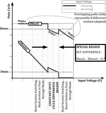
Figure 9.11: The constant difference duty cycle method for controlling the four-switch Buck-Boost (~5 V–5 V case).
The above pattern is completely reversible/retraceable as indicated in Figure 9.11. The duty plots shown are actually overlapping for the cases of VIN falling and VIN rising; the path can be fully retraced from any input voltage point, even within the “special region.”
Part 5: Auxiliary Rails and Composite Topologies
We have just seen how the Buck and Boost topologies can be literally mated to produce the four-switch Buck-Boost. One obvious disadvantage of that approach is that we have positioned a Buck at the input and a Boost at the output. But unfortunately, we know that the Buck topology exhibits a significant RMS current in its input cap, due to the chopped current waveform at that location. And for the same reason, the Boost has significant RMS current passing through its output cap. The four-switch Buck-Boost therefore combines the worst of the two topologies in this regard. We need to ask: can we reverse the order? Would a Boost-Buck composite be better than a Buck-Boost composite? We know that the Boost and the Buck have low RMS currents in their input and output caps, respectively. So our hopes are high as we generate three Boost-Buck composites on these pages: the Cuk, the Sepic, and the Zeta topologies. We will see that in fact we do get low RMS input and output cap currents for the Cuk topology. Unfortunately, the Cuk can’t shake off the “polarity inversion” weakness of its constituent Buck-Boost cell and is therefore usually not favored commercially for that reason. The two other Boost-Buck composites, the Sepic and the Zeta, are both noninverting step-up/step-down topologies. The Sepic is basically the Cuk with a brute-force re-referencing of output rails (with respect to the input). Unfortunately, in the course of correcting the polarity inversion of the Cuk, the Sepic ends up with high RMS current in its output cap, whereas the Zeta has a high RMS current in its input cap. We realize that the perfect switching power topology remains elusive.
The good news is we intuitively expect, and get, the same DC transfer function for all three Boost-Buck composites, as for the (four-switch) Buck-Boost composite, and for the basic (fundamental) Buck-Boost topology. In the present case, we have
![]()
One obvious problem of this rearrangement of constituent topologies to form a Boost-Buck is that the inductors of the Buck and Boost stages are no longer back to back, and therefore we are not able to meld them into one inductor as we did for the four-switch Buck-Boost. So, now we get two inductors. Luckily, it turns out that we can combine the switches of the Buck and Boost cells into one (with single duty cycle). One last question remains: how do we pass energy between the cells? We tap into a swinging node of the Boost cell, and inject that waveform into the Buck cell, via a “coupling capacitor.” So in all, we now expect two inductors, one switch and a coupling cap, in all three Boost-Buck composites.
At this point, we should be getting worried about the stresses in the coupling cap, since all the power coming out of the converter needs to pass through this component. But we will discuss the stresses in that later. For now, we realize that the presence of a coupling cap also gives us a great opportunity. We recall that a fundamental single-inductor Buck-Boost topology has a limitation in that the output has an inverted polarity compared to the input. But we learned that if we use a transformer, we create the flyback topology which physically separates the output section from the input section. Thereafter, we could isolate those sections for safety reasons, as in AC–DC converters, but we could also reconnect them back together, so as to correct the polarity inversion. That is how we get a noninverting, nonisolated flyback. Similarly, a capacitor also gives us the possibility of separating the input and output sections, then re-referencing the output with respect to the input. We thus derive the noninverting Sepic topology from the Cuk. Note that to keep things simple, we will not be getting into synchronous versions of any of these Boost-Buck composites here.
Is It a Boost or Is It a Buck-Boost?
Before we discuss the Cuk and Sepic, we need to understand the basic Boost and Buck-Boost topologies better. Looking at Figure 9.12, we will realize that they belong to the same “super-schematic.” We create the difference by the way we choose to extract energy from the circuit. In fact, by using separate output diodes we can generate two outputs simultaneously, from the same circuit (even though we would be able to regulate only one of them).
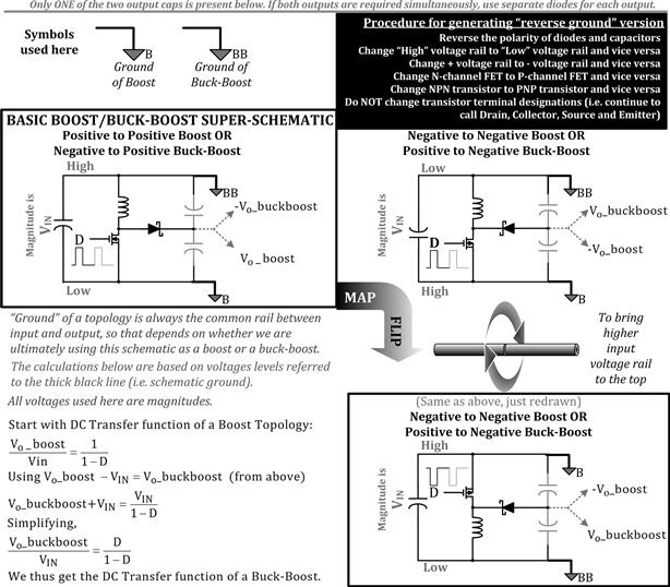
Figure 9.12: The “super-schematic” from which the Boost and Buck-Boost topologies can be derived and the method of mapping common polarity topologies to their reverse polarity counterparts.
A numerical example will make this clearer. Suppose we take a 12-V input Boost converter and apply a duty cycle of 50% to it. We expect to get a Boosted output rail equal to twice the input voltage, that is, 24 V in our example here (use VO/VIN=1/(1−D)). Now, in a Buck-Boost, we would be drawing output energy not from the 24-V Boosted rail and ground, but from between the 24-V Boosted output rail and the 12-V input rail. Eventually, we would call that a negative-to-positive Buck-Boost because, by convention, the rail common to the input and output is the topological ground — and so the 12-V input rail would be renamed the “ground” for the Buck-Boost topology, whereas the input ground of the Boost topology would now become the −12-V input rail of the Buck-Boost. Note that in our example, the Buck-Boost output voltage would then be 24−12=12 V. So, if Figure 9.12 is to be believed, we expect a −12-V to 12-V Buck-Boost to result when switching with a duty cycle of 50%. But that is completely consistent with what we know of a Buck-Boost topology: if we switch it with D=50%, we expect the output voltage to equal the input voltage in magnitude (use VO/VIN=D/(1−D)). So, Figure 9.12 must be right. But if not fully convinced, we can repeat the above numerical example for any D, and we will realize that the Buck-Boost and Boost are truly part of the same super-schematic shown in Figure 9.12. No wonder that both the Boost and the Buck-Boost share another valuable property: the center of inductor current in both cases is IO/(1−D).
In Figure 9.12, we go a step further. Starting with the super-schematic on the left, that would give us a positive-to-positive Boost and a negative-to-positive Buck-Boost, we generate a super-schematic that gives us a negative-to-negative Boost and a positive-to-negative Buck-Boost.
Note: Historically, voltages used to be referred to with the higher potential being labeled ground, and the rest of the circuit “hanging” from it, much like a clothesline. These were “positive-ground” systems. Nowadays, the world has shifted largely to “negative-ground” systems, where the ground is the lower rail. So a modern-day circuit generally resembles a skyline, not a clothesline. However, in creating and recognizing composite topologies, we need to understand how a negative-ground circuit, or cell, can be mapped into its positive-ground equivalent. A simple mapping procedure, outlined in Figure 9.12, is required. Using that procedure, we generate the corresponding positive-ground super-schematic. Finally, since the mapping procedure changes high voltages to low voltages, and vice versa, to get back to our familiar convention of placing higher voltages on top of the page, we flip the positive-ground super-schematic vertically, as shown in Figure 9.12, to arrive at the more conventional way to draw a negative-to-negative Boost (and positive-to-negative Buck-Boost).
Understanding the Cuk, Sepic, and Zeta Topologies
In Figure 9.13, we first start by blindly cascading a Boost with a Buck. In the middle of the circuit, we have a DC rail bridging the two, over which power flows down, from one to the other converter. It uses two switches, and the challenge is to combine those into one. In the following three schematics, we do just that, by connecting to the switching node on either side by a coupling cap. Note that on the right side, we map each composite topology to its reverse voltage counterpart as discussed above. So we can generate a negative-to-positive Cuk or a negative-to-negative Sepic if we so desire.
Note: Though in the standard mapping process, we change an N-channel FET to a P-channel FET, all topologies, mapped or otherwise, can be implemented with either type of FET — we just have to keep track of the Gate voltages required, and if necessary, provision for a bootstrap circuit. Also, we need to pay attention to the direction the internal body-diode is pointing so as to avoid the “killer voltage spike” we often talk about. In an N-channel FET, the body-diode (considered as an arrow from anode to cathode) points from Source to Drain. In a P-channel FET, it points from Drain to Source.
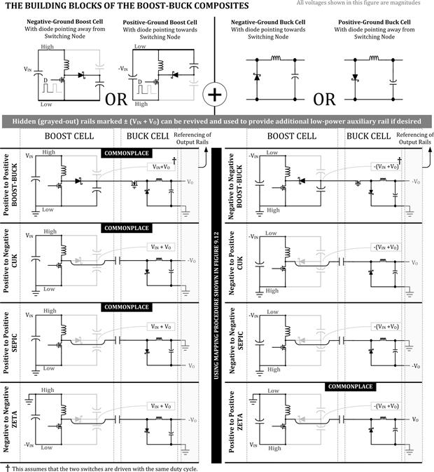
Figure 9.13: Combining the positive and negative Boost cells with positive and negative Buck cells to generate various Boost-Buck composite topologies.
Each circuit actually has three sections: a Boost cell, followed by a Buck cell, followed by a block labeled “Referencing of Output Rails.” This latter block is where we can set virtually any output polarity as discussed previously. However, unlike transformer-based isolation as in a flyback, this re-referencing dramatically alters the path of currents as shown in Figure 9.14. The reason for that is in a transformer, there is no net flow of current between the two separated sections — and the output (Secondary) section can function on its own since both the forward and the return paths get disconnected by the transformer winding. But in capacitor coupling, the current path still exists, and so by re-referencing, that pattern can get completely changed. We therefore get three distinct topologies, with some remarkably different behaviors, but also with great similarities based on their common heritage: the Cuk, Sepic, and Zeta. As mentioned previously, we can look upon the Sepic as a brute-force attempt to correct the polarity inversion of the Cuk. And it worked. Though again, as mentioned previously, this introduced high RMS currents into the output cap.
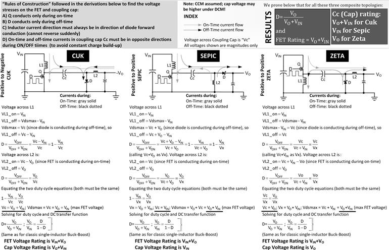
Figure 9.14: The duty cycle and voltage ratings of components of the Boost-Buck composites.
In Figure 9.14, we calculate the DC voltage level appearing across the coupling capacitor in each composite topology, so we can pick its voltage rating better. The general “rules of construction” by which we have unequivocally generated the paths of currents shown during the ON-times and OFF-times, respectively, are bulleted out in the same figure. We thereby show that, similar to the fundamental Buck-Boost topology, the DC transfer of all these composite topologies is D/(1−D), just as we had inituitively expected. And similarly, the minimum voltage rating of the FET in all cases is the same: VIN+VO. Note that in any switching topology, in general, if the switching FET blocks a certain voltage across it when it is OFF, then when it turns ON, that same voltage blocking responsibility gets literally transferred over to the diode, which must therefore be rated identically. In other words, the diode too must be rated VIN+VO for all the three Boost-Buck composite topologies under discussion.
In Figure 9.15, we have first drawn the Sepic and Zeta topologies in a more conventional manner. We see that the similarities between the waveforms of these composite topologies are tremendous. It is a result of their common heritage as brought out more clearly in Figure 9.14.
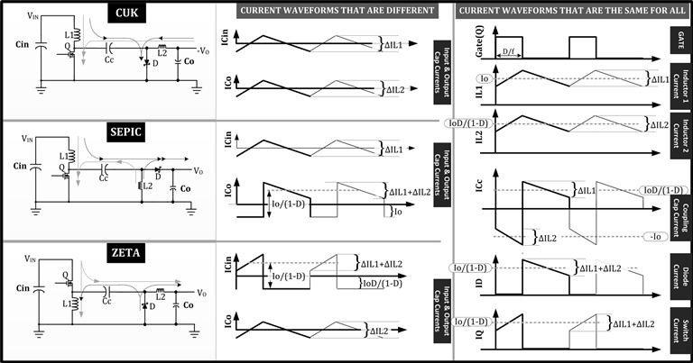
Figure 9.15: Current waveforms in the Boost-Buck composites.
The current waveforms in the figure can be easily guessed based on some simple reasoning described in the next section. From Figure 9.15, we see that the only difference in the current waveforms is in the input and output capacitors. In all the other components, except for the coupling capacitor, both the required voltage and the current ratings are the same for all three topologies. This is also discussed further below.
Generating the Current Waveforms of the Cuk, Sepic, and Zeta Converters
Cuk: We refer to Figure 9.15. The center of ramp of IL2 must be IO (output current) since it is the constant current flowing in from the output. So,
![]()
During the ON-time, this current passes through Cc. In the OFF-time, IL1 flows through the cap in the opposite direction. Since the cap is in steady state, its change in charge during the ON-time must be equal and opposite to the change in charge during the OFF-time. Therefore, the following equality must be true:
![]()
Therefore,
![]()
The current in Q during the ON-time is the sum of the two currents, IL1 and IL2. So,
![]()
The current in the diode during the off-time is also the sum of IL1 and IL2. So, its center of ramp is also IO/(1−D), as for the switch.
We see that the switch current is the same as for a fundamental Buck-Boost in terms of its height and duration. Note that in a Buck-Boost, there is a single inductor of rating IO/(1−D). Here we have two inductors, one rated IO, the other IOD/(1−D). For example, if we set IO=1 A and D=0.5, in the fundamental Buck-Boost, the inductor must be rated at least 2 A (ignoring the ramp portion here). In the Cuk, we need two inductors, each rated 1 A. For the same inductance, the total core volume for the Cuk is actually half that of the Buck-Boost, since core volume is proportional to LI2. However, if we keep the same current ripple ratio r, then if the current goes from 2 A to 1 A, we need to double the inductance (the usual scaling law for inductors). So for the case of constant r, there is no net change in the total core volume in going from the Buck-Boost to the Cuk. In fact, using two inductors instead of one will provide greater surface area exposed to natural convection, which will help in high-power applications by improving the thermal dissipation. These arguments are valid for the Sepic and Zeta too.
Sepic: We refer to Figure 9.15. The output current flows in spurts through the diode during the OFF-time only (further averaged by the output cap). We have two contributions to the diode current. Together, they must average out to IO. So,
![]()
Coming to the coupling cap, IL1 flows through it in one direction during the OFF-time, and IL2 flows through it in the opposite direction during the ON-time. So, by equality of charge in steady state we get
![]()
Solving the two equations above, we get as for the Cuk
![]()
The current in Q during the ON-time is the sum of the two currents, IL1 and IL2. So,
![]()
The current in the diode during the off-time is also the sum of IL1 and IL2. So, its center of ramp is also IO/(1−D) as for the switch.
Zeta: We refer to Figure 9.15. Looking at the coupling cap first, we have two currents going through it in opposite directions during the ON-time and OFF-time, respectively. The current during the OFF-time passes through L1 and is the only current component in that. So, it must equal IL1. The current through the cap during the ON-time does not go through L1. But it is the only current component through L2 during the same time. So, it is by definition equal to IL2. We therefore have by charge balance in the coupling cap
![]()
Note that the output is in series with L2, and the current in an inductor cannot change suddenly. So, from the current through L2 during the OFF-time, we get
![]()
Plugging this into the preceding equation we get
![]()
The current in Q during the ON-time is thus the sum of the two currents, IL1 and IL2. So,
![]()
The current in the diode during the off-time is also the sum of IL1 and IL2. So, its center of ramp is also IO/(1−D) as for the switch.
Stresses in the Cuk, Sepic, and Zeta Topologies and Component Selection Criteria
We see a remarkable pattern emerge. The current waveforms of the switch and diode in all three Boost-Buck topologies are identical and are also the same as in the fundamental single-switch single-inductor Buck-Boost. We also know their duty cycle equations and voltage ratings of switch and diode are the same. That lays credence to our initial claim that these are just composites of a Boost (or equivalently of a Buck-Boost) cell and a Buck cell.
Ignoring the AC ripple component here, we see that the switch current is a rectangle of height IO/(1−D) and width D/f. So its RMS must be
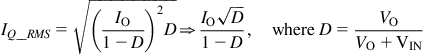
Using D=VO/(VO+VIN), we can also write this as
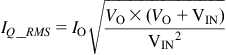
The average current through the diode is
![]()
Note that we have to follow the general design guidelines for a fundamental Buck-Boost topology. We realize that in this case too, the RMS current through the switch is a maximum at Dmax (lowest VIN). We already know the voltage ratings of the FET and diode in all Boost-Buck composites need to be better than VO+VIN (see Figure 9.14). The latter needs to be checked at Dmin (highest VIN).
The RMS current through the coupling cap needs to be calculated also. In all Boost-Buck composites, we have IL2 flowing through the coupling cap during the ON-time and IL1 flowing in the OFF-time (opposite direction). However, for calculating RMS, the sign of the current does not matter since we use I2. So, using our side-to-side segments summation formula of Figure 7.4, we get

Using D=VO/(VO+VIN), we can also write this as
![]()
Clearly, this is the highest at lowest input (VINMIN), and the cap RMS rating should be picked accordingly. We already know the voltage ratings of this cap to be VO+VIN or VIN or VO respectively, in the Cuk, Sepic, and Zeta topologies (see Figure 9.14). These need to be verified at maximum input (VINMAX).
For the RMS current ratings of the input and output caps of these Boost-Buck composites, we note that for a Cuk, we can ignore both these RMS currents since they are very small, whereas for the Sepic we can ignore the input cap RMS, and for a Zeta we can ignore the output cap RMS. For the output RMS of the Sepic, we can use the formula given in the Design Table of the Appendix for a Boost (or Buck-Boost) output cap. For the input RMS of the Zeta, we can use the formula for a Buck-Boost input cap. That completes the calculation of stresses for all three composite topologies, and we can pick them appropriately.
As for L1 and L2, as is our usual practice, we target a current ripple ratio r of 0.4 for both these inductors at VINMIM (Dmax). That gives us the required inductance. We already know their current ratings. Note that the voltage waveform across all inductors L1 and L2 of all three Boost-Buck composites are the same (in CCM). We can see this from Figure 9.14 that in all cases
![]()
This was the historical reason why Mr. Cuk decided to try to “save an inductor” by winding L1 and L2 on the same core (in the converter subsequently named after him). To his surprise, he discovered that, depending on how the windings were placed on the core (the coupling coefficients), the ripple current in either the input cap or the output cap, or both, could be reduced very close to zero. This is called “ripple steering.” It is the subject of great academic attention, but is still not really used commercially on a wide scale, perhaps because (a) the input/output cap RMS currents in the Cuk converter are very low to start with, (b) it is hard to guarantee coupling coefficients in mass production (and any non-guaranteed advantage is really no advantage in the commercial arena), and (c) with the advent of low-ESR caps, the heating in the input/output caps of a Cuk converter is virtually negligible to merit any further attention. Note that if this is done, it is commonplace to use the same number of turns for both L1 and L2, and so, their ripples (not their ripple ratios) will become identical. This can pose a problem at light loads because one inductor will go into DCM before the other. It can also cause different voltage stresses on the components than expected. Note that we have assumed CCM all through our previous discussions. However, since ripple steering is not commonly used, we will avoid further discussion on this shared-core approach.
Part 6: Configurations and “Topology Morphology”
In this section, we return to the basics armed with our recently acquired knowledge, and see what more we can do with our basic topologies. Here we first distinguish between a topology and a configuration. For example, a regulator converting 12 V to 5 V is a positive-to-positive configuration of a Buck topology. But we could have a regulator converting −12 V to −5 V, and that would still be a Buck regulator, but a negative-to-negative configuration.
In Figure 9.12, we learned how to map a negative-ground configuration to a positive-ground one. However, we know that in power supplies we may end up redesignating the ground rail anyway, as it needs to be the common rail between the output and the input. Further, we could also end up replacing a P-channel FET with an N-channel FET, and vice versa, so long as we can drive it appropriately. For these reasons, we should not get fixated on the fact that a given circuit is either “positive ground” or “negative ground.” That itself may not matter at all. But the mapping procedure to get from one to the other is critical in generating the different configurations of topologies, because we have learned that the mapping procedure changes positive voltages to negative voltages and vice versa. That fact is the one to remember and use.
In Figure 9.16, let us take the positive-to-positive Buck for example. We can do this either by an N-channel FET or by a P-channel FET. In the former case, we would need a bootstrap rail to drive the FET when the FET turns ON. Let us now look at the negative-to-negative Buck. We see that we can do this, once again, either by an N-channel FET, or by a P-channel FET. But this time, in the former case we do not need a bootstrap rail to drive the FET. However, we need a bootstrap for the P-channel FET now. We thus realize that all “high-side” configurations (where the FET is placed toward the high-side rail) are more easily driven by P-channel FETs, whereas “low-side” configurations are more easily driven using N-channel FETs. Otherwise, a bootstrap will be required in both cases.
Figure 9.16: Configurations of the three basic topologies by the mapping procedure.
Let us now do a mapping procedure on the positive-to-positive Buck using an N-channel FET. We realize that after mapping as per Figure 9.12, it becomes a negative-to-negative Buck using a P-channel FET. Furthermore, the drive waveform also gets flipped vertically, and positive becomes negative, and vice versa. Also, if there was a bootstrap to start with, it remains one after mapping. If no bootstrap was required initially, after mapping too, no bootstrap will be required. This way we can easily generate all the possible configurations shown in Figure 9.16.
Having understood this, we move on to “topology morphology.” This relies on the basic fact that a switcher is just a switcher. In all cases, we are basically toggling (switching) a FET with a certain duty cycle, and then applying a feedback signal to control the output level. So, there seems no reason why we can’t, at least theoretically speaking, use a switcher IC meant for one configuration, for another configuration. We may, however, need to do a voltage translation or differential sense of the output and apply it to the IC, since in all likelihood, the IC ground, which is the reference rail of its internal error amplifier and other circuitry, may be different from the ground of the topology. Is that all? No, there is one more condition. Just the way the topologies are, there is a difference in high-side and low-side topologies as far as the diode direction is concerned. If we look closely at Figure 9.16, we will see that in all low-side configurations, be it with an N-channel or a P-channel FET, the switching node (i.e., the common node shared by the switch, diode, and inductor) is always connected to the anode of the diode, whereas in high-side configurations, the switching node always connects to the cathode. This implies that we may be able to use an IC meant for a high-side configuration, in any high-side configuration, irrespective of topology. Similarly, an IC meant for low-side configuration may be used in any low-side configuration. We may need to bring the feedback signal to it appropriately, and also remain conscious of the new voltage and current stresses as we change topologies (thus ensuring those are still within the capability of the IC). If we ensure all that, the IC will not know the difference as we morph the circuitry around it into another topology. We are ignoring loop stability issues here.
We now look around and realize that, in essence, we deal with only two basic types of IC constructions commonly. One is meant for a positive-to-positive Buck converter. This is a high-side configuration. The other is a positive-to-positive Boost converter, that being a low-side configuration.
Note: We know that the Boost and Buck-Boost are part of the same super-schematic and also that the Cuk, Sepic, and Zeta are all Boost-Buck composites. Which is why we generally expect that, with only minor modifications, we can always use a “Boost IC” for Buck-Boost, Cuk, Sepic, and Zeta applications (with the same intended high-side or low-side configuration).
In Figure 9.17, we take each of these two ICs and generate all the possibilities. We note that a positive Buck IC with a P-channel FET can easily do a positive-to-negative Buck-Boost or a negative Boost because all three are high-side configurations of P-channel FETs as per Figure 9.16. Similarly, a positive Boost IC with N-channel FET is a low-side configuration and can therefore do a negative Buck or a negative-to-positive Buck-Boost, simply because all these are low-side configurations. In other words, we have several configurations that are mutually natural cousins. However, there is an interesting trick that we can use to force a low-side IC (e.g., a positive Boost IC) into doing high-side configurations such as the positive Buck. These are also shown in Figure 9.17 as “forced configurations”. But there are limitations to this approach as indicated in the figure (poor regulation/noise).
Figure 9.17: Topology morphology using the two common types of ICs in use today.
Note that in all cases, as we morph topologies, not only do the current and voltage stresses/ratings need to be re-evaluated to confirm the new application of the IC, we should also pay attention to possible changes in stability (loop behavior) and ensure we can make the transition in a stable manner. If we have an external compensation pin, that can greatly help in our endeavor.
Part 7: Other Topologies and Techniques
Hidden Auxiliary Rails and Symmetry
In the topmost schematic of Figure 9.13, we mentioned that a brute-force composite of a Boost converter followed by a Buck converter has an intermediate rail of value VO+VIN. We added a footnote to say that results when the duty cycle of the Boost stage equals the duty cycle of the Buck stage. In other words, the Gates of the two FETs shown are, virtually speaking, tied together (they go ON and OFF in unison). The math behind that is shown more clearly in Figure 9.18. We see that we have a low-power regulated rail of value VO appearing across the Boost inductor. Though it is not ground referenced, we can use it in some situations. For example, we can place an LED to indicate that the Boost stage is really switching. We can also try to regulate that auxiliary voltage rail in preference to the main output rail. This can be of use in an opto-less Primary-side sensing scheme in AC–DC power supplies, with the Buck stage replaced by a Forward converter. In the Cuk, Sepic, and Zeta converters too, we have this hidden VIN+VO rail, and it can be revived for low power if we want. In the lower half of Figure 9.18, we briefly present a novel AC–DC converter idea from the author, which does not require an input bridge rectifier. It goes to show that when we understand the three basic topologies better, we may not invent a radically new topology, but there is still a lot we can do by just rearranging the building blocks.
Figure 9.18: The brute-force Boost-Buck composite with an auxiliary rail, and the symmetric Boost topology.
Multiple Outputs and the Floating Buck Regulator
Another challenge is to generate multiple outputs from a single converter. In any single-switch power supply, there is always one control loop and one corresponding duty cycle. So, we get one output that is well regulated. Many attempts abound into generating multiple outputs that closely “follow” the main regulated output closely. In Figure 9.19, we collect some of the techniques used in AC–DC power supplies. They are based on the volts/turn law of a transformer, which says that at any moment, a perfect transformer has identical volts per turn on any of its windings. Of course, there is no perfect transformer. We have to counter the effects of DC resistance as we pull current from the windings, and also leakage inductance effects between the windings. The former is tackled by using fairly thick wire, and the latter will include techniques to tightly couple the Secondary windings together. Also, when we draw current from the main winding, it goes through a diode, whose forward-drop depends on current and temperature. For example, if we draw a lot of current, the drop is more. So, the control loop compensates for that drop by pushing the average volts/turn in the transformer higher (by increasing the duty cycle). That causes the other outputs to increase too, even though they do not need that correction. Therefore, one way of compensating for this effect is to have the bottom end of the Secondary winding connect to the cathode of the main output diode, as shown in the figure. Now, as the drop across the diode increases with load, it pulls the other output down somewhat, compensating partially for the higher average volts/turn in the transformer. Other ways include trying to do a sort-of weighted control loop that is lightly affected by outputs other than the main one.
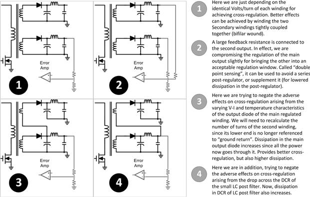
Figure 9.19: Deriving cross-regulated outputs from the main transformer in AC–DC power supplies.
In Figure 9.20, we show a common technique to derive power for Secondary-side housekeeping circuitry in AC–DC power supplies. A winding is thrown across the output choke. That is straightforward. We can do the same with a Buck converter as shown. However, we can then try to have the Buck converter ride on top of the very rail it generates. That changes the Buck topology into a “floating Buck regulator.” We have reduced voltage stresses on the switch and controller IC, and we also have an auxiliary rail to use if desired. In the earlier cases, if we use a turns ratio of 1:1, the voltage on the auxiliary rail will be VO (same as the main rail). In the floating Buck regulator, the auxiliary voltage is exactly half the voltage of the main rail (i.e., VO/2).
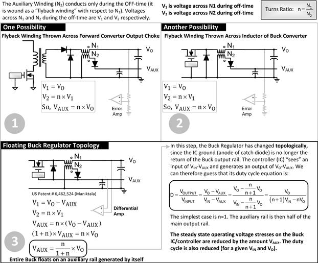
Figure 9.20: Deriving auxiliary outputs from the output choke/inductor of the Forward/Buck converter and understanding the floating Buck regulator topology.
In AC–DC power supplies, we can put many windings on the transformer, and by the fact that each winding will (or should) have the same volts/turn, we can predict the voltage of other windings placed on the same core as the main controlled-output winding. In principle, we get many regulated outputs. In practice, because of parasitics and leakage inductances, the relative regulation of the output is not very good. There are many ways to handle this as indicated in Figure 9.19.
Hysteretic Controllers
Looking back at Figure 1.2, the bucket regulator and its SCR-based version are early examples of “bang-bang regulators.” A vague control loop exists that turns ON the semiconductor if the voltage falls below a certain threshold and turns it OFF if the voltage exceeds a certain threshold. There is no predictable waveform in the process. But there is also no reason why we can’t try out the same technique (or lack thereof), using a conventional Buck regulator (or even other topologies). At least the new candidate uses an inductor, so it promises much higher efficiency. Whenever the voltage falls below a certain threshold, we would command the controller to switch with its maximum duty cycle. After a while, the output would rise and cross the upper threshold, at which point all switching would stop. This type of controller would have excellent transient response since it turns on full-blast (with full duty cycle) whenever needed, and turns OFF equally dramatically when not needed. We wouldn’t have to worry about complicated poles and zeros. We would likely save a lot of die area in a controller of this type since there is no compensation circuitry or PWM comparator. But the main problem here is possible inductor saturation and “pulse-bunching.” We could get a string of full-width pulses, and then none, creating almost any pattern. We would therefore likely generate highly unpredictable EMI, and audible noise too (from magnetic components and ceramic/film capacitors).
For better results, we would like to have a steady stream of pulses instead of pulse-bunching. Further, to minimize die area and reduce quiescent current, it would also be nice to get rid of the clock entirely. How do we start by doing the latter? We realize that we have an inherent clock present in any converter, based on its switching natural time constants. For example, we know that the inductor current undulates at a regular rate, determined by the applied voltages and the inductance. That is in effect a clock. So, can we use that instead of a formal clock circuit? If so, where can we extract the signal from? If we assume that the output cap of the Buck has no significant ESL, but just resistance (ESR), it has a voltage ripple riding on top of the DC output voltage. The ripple has the same periodicity as the inductor current and also the same duty cycle that we want to drive the switch with. It thus becomes a candidate for trying to invert cause and effect. This cap voltage ripple becomes the (scaled) voltage applied to the feedback pin of the controller IC. So now, if we set min and max thresholds on the feedback pin, we could generate the very inductor waveform that we are sensing — a self-stabilizing chicken and egg situation at an electrical level, one that could last forever. That is the only naturally stable situation that can result with the bare constraints applied. This process is shown in Figure 9.21. We also see how the frequency can be changed by varying the hysteresis between the upper and the lower thresholds. Note that any asymmetry in the thresholds will translate into a DC offset error on the output.
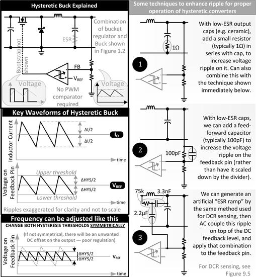
Figure 9.21: Hysteretic control and changing switching frequency.
In reality, we know that ceramic caps in use today have very low ESR. So, the ripple on the output cap of a Buck can be very small and can also vary a lot. So, various techniques have emerged in trying to generate a proper “ESR-ramp” as outlined in Figure 9.21.
One of the problems of these hysteretic Buck regulators is that their frequency can vary a lot. Various techniques exist, some proprietary, to minimize the DC offset mentioned above and also to maintain constant frequency — all hopefully without excessively complex circuitry which would end up negating the very reason for considering hysteretic regulators — low quiescent current, good transient response, and optimized silicon area and cost.
Besides varying the hysteresis band as indicated in Figure 9.21, there is another method for trying to achieve fairly constant frequency using hysteretic controllers. This is called “constant on-time” (COT) control.
For a Buck topology, we can do the following interesting analysis:
![]()
So,
![]()
Using
![]()
![]()
![]()
In other words, if we force a constant on-time, but one that is inversely proportional to input voltage, then for a given output voltage we will get constant frequency. So, in this type of control, whenever the feedback voltage falls below a set threshold, the FET is turned ON. However, the FET is not turned OFF based on any ESR-based ripple crossing an upper threshold. Instead the FET literally “times out” because the ON-pulse is generated by a simple, one-shot flip-flop (a monostable multivibrator). Remember that this hysteretic implementation also has no clock. After the FET turns OFF, then after a small, arbitrary, guaranteed OFF-time, if the feedback voltage is still below the set threshold, another one-shot pulse will follow, otherwise the pulse will be skipped. And so on. Eventually, the converter will settle down somewhat close to a steady stream of pulses. With a simple input-feedforward circuit, the width of the one-shot can be varied inversely with respect to input voltage. So finally, the frequency will be roughly constant with respect to both line and load variations.
Can we invoke constant frequency in a hysteretic Boost? Here is the math.
![]()
![]()
We can thus eliminate TON
![]()
![]()
![]()
Or
![]()
Using
![]()
![]()
![]()
Or
![]()
In other words, in a Boost, if we fix TOFF for a given input voltage, and then vary TOFF such that it is proportional with respect to the input voltage, then for a given VO, f is a constant. This would be a constant frequency, constant off-time (also confusingly called “COT”) Boost regulator.
Note that in Chapter 12, we discuss the causes of the RHP (right half plane) zero in the Boost and Buck-Boost topologies (operating in CCM). The intuitive reason for that is under a sudden load demand, the output dips momentarily, and therefore the duty cycle increases. But in the process, the off-time decreases. Since in both these topologies, energy is delivered to the output only during the off-time, a smaller off-time leaves less time for the new energy requirement to be met, which temporarily causes the output to dip even further before things get back to normal. So clearly, fixing a certain minimum off-time will help. The RHP zero is not present when operating in constant off-time mode. Further, in a Boost, we can get constant-frequency operation too as described above.
Don’t even bother to do the math for creating a constant-frequency hysteretic Buck-Boost. The requirement is neither constant on-time nor constant off-time, but a complicated function of both VIN and VO. Therefore, its implementation, if any, will just sacrifice the expected simplicity of hysteretic control.
Pulse-Skipping Mode
All the above discussions assume CCM, in which the duty cycle is almost constant with respect to load and inversely proportional to input voltage (in a Buck). So, what happens to a COT Buck converter if the load is decreased? The one-shot generator will continue to produce CCM-based one-shot pulses, whereas in conventional DCM, the pulse width decreases rapidly with load, if not forcibly disallowed. So in effect, with COT at light loads, we would end up pumping far more energy per pulse than demanded by natural DCM. The control loop will therefore see the output rising suddenly, and try to arrest that rise by skipping several pulses in succession. We thus get “pulse-skipping mode.” There are many ways to implement this feature, but the basic advantage is reduced switching losses, which are a major factor in the low-efficiency readings at light loads of synchronous converters, with complementary drives in particular. IC designers also try to take further advantage of the relatively long OFF-times, and “de-bias” some of their circuits, to reduce the quiescent current of the IC too, and maximize efficiency at light loads. For example, the FET Gate drives may no longer be held down “hard,” but rather softly so. And so on. The challenge, however, is to wake up all hibernating circuits very rapidly when the load demand increases, so as not to cause output glitches as the converter moves from pulse-skipping mode to full CCM operation. One cause of output glitches is due to the system, considered purely as a power processing stage, transitioning between an artificially enforced mode and natural CCM operation. At the transition boundary, the energy levels in the capacitors and inductor need to restabilize to their new steady-state values. Till that happens, the output will either overshoot or undershoot. However, one of the best ways of avoiding this particular type of output glitch is the “duty cycle brickwall” method of implementing pulse-skipping. This is the least intrusive method and simply sets a minimum duty cycle for the converter to obey. As the load is decreased, DCM is initially entered and the duty cycle starts to progressively decrease as load is further reduced. But at some point, the duty cycle hits a brickwall, and is not allowed to shrink further. The system then, very naturally, starts skipping pulses to maintain energy balance. If however the load is increased, equally naturally, the system exits this pulse-skipping mode. The way to tradeoff output ripple and efficiency is to carefully position this brickwall, by defining the appropriate “m-factor” below.
![]()
A typical value of m could be between 50% and 85%. This forces a natural minimum duty cycle, and the converter goes in and out of pulse-skipping mode smoothly.
Achieving Transformer Reset in Forward Converters
Finally, to close with the somewhat mundane, and also tie up some remaining loose ends, we return to the single-ended Forward converter with an energy recovery (tertiary) winding. In Figure 9.22, we indicate that the position of the energy recovery winding diode can affect converter efficiency too. This was previously touched upon in Chapter 7. In a conventional single-ended Forward converter, by using a 1:1 ratio between the Primary (“PRI”) winding and the tertiary (“TER”) winding, we ensure that the rising slope of the magnetization current VIN/LPRI is equal in magnitude to the falling slope VIN/LTER, since LPRI=LTER. So, we need to ensure a maximum duty cycle of 50%, which leaves just enough time, even in the worst case, for the magnetization current to slope down to the value it started the cycle off with (zero in this case). That is termed transformer “reset.” By achieving reset, we ensure the transformer can operate in steady state with no flux-staircasing. The impact of this is that the voltage stress on the FET is exactly 2×VINMAX under all load conditions. However, a 50% max duty cycle is easily achieved by popular controllers like the UC3844, by using a frequency doubler circuit. Basically, the internal clock of the IC runs at 2×fSW, and every alternate cycle is blanked out. During that blanked-out interval, the FET is forced OFF. So, in effect, the max ON-time (the nonblanked-out interval) can never exceed the OFF-time, and reset is assured.
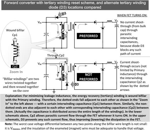
Figure 9.22: Position of the energy recovery diode can affect Forward converter efficiency.
In Figure 9.23, we also show how the “active clamp Forward converter” works, and its relative pros and cons. Similar to the asymmetric half-bridge (i.e., the two-switch Forward converter, see Table 7.1), it doesn’t have an additional energy recovery winding. But nor is it restricted to a max of 50% duty cycle. In this case, it is of paramount importance to fix the maximum duty cycle by using a well-designed control circuit, since DMAX determines the max voltage stress on the FET: VINMAX/(1−DMAX). If DMAX approaches 1, the voltage stress will approach infinity. Observe that the clamp circuit basically runs like a synchronous Buck-Boost stage, the “output” of which is the voltage of the clamp capacitor. So, as in any Buck-Boost, we can predict that the output rail (the voltage on the clamp capacitor in this case) is
![]()
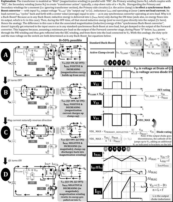
Figure 9.23: The active clamp Forward converter.
With that we close our sojourn into the exciting world of “new topologies,” as we wait for more to be discovered. However one thing remains clear. Figure 1.15 is still irrefutable — there are only three fundamental topologies. The rest are, on deeper thought, variants or combinations of the basic three. This chapter should have made that quite clear by now. The key to understanding “new” or exotic topologies also lies therein.