
Chapter 12
Feedback Loop Analysis and Stability
This chapter advances from the very basics to full stability analysis of power converters. Time and frequency domain analyses are first explained along with the s-plane and the underlying concept behind the Laplace transform. Mathematics in the log-plane is described, and passive filter responses are plotted out. The concept of poles and zeros follows. Basic control loop theory is explained, and the plant transfer functions of the fundamental topologies are all derived. Transconductance amplifiers (OTAs) are compared with conventional voltage op-amps, and it is shown how to use them for implementing a feedback section and thereby closing the loop. Types 1–3 compensation techniques are discussed in detail, and ways to carry out pole-zero cancellation to achieve desirable open-loop gain and phase characteristics are explained. Both voltage-mode control and current-mode control are discussed, and detailed numerical examples are included. Extras include a discussion of the RHP zero, subharmonic instability and line feedforward.
Transfer Functions, Time Constant, and the Forcing Function
In converters, we often refer to the steady-state ratio: output divided by input, VO/VIN, as the “DC transfer function” of the converter. We can define transfer functions in many ways. For example, in Chapter 1 we discussed a simple series resistor–capacitor (RC) charging circuit (see top schematic of Figure 1.3). By closing the switch we were, in effect, applying a step voltage to the RC. Let us call the voltage step “vi” (its height).
That was the “input” or “stimulus” to the system. It resulted in an “output” or “response” — which we implicitly defined as the voltage appearing across the terminals of the capacitor, that is, vO(t). So, the ratio of the output to the input was also a “transfer function”:
![]()
Note that this transfer function depends on time. In general, any output (“response”) divided by input (“stimulus”) is called a “transfer function.”
A transfer function need not be “Volts/Volts” (i.e., dimensionless). In fact, neither the input nor the output of any such two-port network need necessarily even be a voltage. The input and output need not even be two similar quantities. For example, a two-port network can be as simple as a current sense resistor. Its input is the current flowing into it, and its output may be considered as the sensed voltage across it. So, its transfer function has the units of voltage divided by current, that is, resistance. Or we could pass a current through the resistor, but consider the response under study as its temperature. So, that would be the output now. Later, when we analyze a power supply in more detail, we will see that its pulse-width modulator (PWM) section, for example, has an input that is called the “control voltage” (output of error amplifier), but its output is a dimensionless quantity: the duty cycle (of the converter). So, the transfer function in that case has the units of Volts−1. We realize the phrase “transfer function” is a very broad term.
In this chapter, we start analyzing the behavior of the converter to sudden changes in its DC levels, such as those that occur when we apply line and load variations. These changes cause the output to temporarily move away from its set DC regulation level VO, and therefore give its feedback circuitry the job of correcting the output in a manner deemed acceptable. Note that in this “AC analysis,” it is understood that what we are referring to as the output or response is actually the change in VO. The input or stimulus, though certainly a change too, is defined in many different ways as we will soon see. In all cases, we are completely ignoring the DC-bias levels of the converter and focusing only on the changes around those levels. In effect, we are studying the converter’s “AC transfer functions.”
How did we actually arrive at the transfer function of the RC circuit mentioned above? For that, we first use Kirchhoff’s voltage law to generate the following differential equation:
![]()
where i(t) is the charging current, q(t) is the charge on the capacitor, vres(t) is the voltage across the resistor, and vcap(t) is the voltage across the capacitor (i.e., vo(t), the output). Further, since charge is related to current by dq(t)/dt=i(t), we can write the above equation as
![]()
or
![]()
To solve this, we “cheat” a little. Knowing the properties of the exponential function y(x)=ex, we do some educated reverse-guessing. And that is how we get the solution:
![]()
Substituting q=C×vcap, we arrive at the required transfer function of the RC-network given earlier.
Note that the differential equation for q(t) above is in general a “first-order” differential equation — because it only involves the first derivative of time.
Later, we will see that there is a better way to solve such equations — it invokes a mathematical technique called the “Laplace transform.” To understand and use that, we have to first learn to work in the “frequency domain” rather than in the “time domain” as we have been doing so far above. We will explain that soon.
Here we note that in a first-order differential equation of the above type, the term that divides q(t) (“RC” in our case) is called the “time constant.” Whereas, the constant term in the equation (“vi/R” in our case) is called the “forcing function.”
Understanding “e” and Plotting Curves on Log Scales
We can see that the solution to the previous differential equation brought up the exponential constant “e,” where e≈2.718. We can ask — why do circuits like this always seem to lead to exponential type of responses? Part of the reason for that is that the exponential function ex does have some well-known and useful properties that contribute to its ubiquity. For example,
![]()
But this in turn can be traced back to the observation that the exponential constant e itself happens to be one of the most natural parameters of our world. The following example illustrates this.
Example:
Consider 10,000 power supplies in the field with a failure rate of 10% every year. That means in 2010, if we had 10,000 working units, in 2011 we would have 10,000×0.9=9,000 units. In 2012, we would have 9,000×0.9=8,100 units left. In 2013, we would have 7,290 units left, in 2014, 6,561 units, and so on. If we plot these points — 10,000; 9,000; 8,100; 7,290; 6,561; and so on, versus time, we will get the well-known decaying exponential function. See Figure 12.1. We have plotted the same curve twice: the curve on the right has a log scale on the vertical axis. Note how it now looks like a straight line. It cannot, however, ever go to zero! The log scale is explained further.
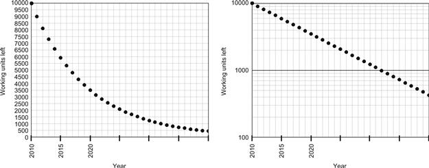
Figure 12.1: How a decaying exponential curve is naturally generated.
Note that the simplest and most obvious initial assumption of a constant failure rate has led to an exponential curve. That is because the exponential curve is simply a succession of evenly spaced data points (very close to each other), which are in simple geometric progression — that is, the ratio of any point to its preceding point is a constant (equal intervals). Most natural processes behave similarly, and that is why “e” is encountered so frequently. In Chapter 6, we had introduced Arrhenius’ equation as the basis for failures. That too was based on “e.”
We recall that logarithm is defined as follows — if A=BC, then logB(A)=C, where logB(A) is the “logarithm of A to the base B.” The commonly referred-to “logarithm,” or “log,” has an implied base of 10 (i.e., B=10), whereas the natural logarithm “ln” is an abbreviation for a logarithm with a base “e” (i.e., where B is e=2.718). We will be plotting a whole lot of curves in this chapter on “log scales.”
Remember this: if the log of any number is multiplied by 2.303, we get its natural log. Conversely, if we divide the natural log by 2.303 we get its log. This follows from
![]()
Flashback: Complex Representation
Any electrical parameter is thus written as a sum of real and imaginary parts:
![]()
where we have used “Re” to symbolically denote the real part of the number A and “Im” for its imaginary part. From these components, the actual magnitude and phase of A can be reconstructed as follows:
![]()
![]()
Impedance too is broken up into a vector in this complex representation — except that though it is frequency dependent, it is (usually) not a function of time.
The “complex impedances” of reactive components are
![]()
![]()
To find out what happens when a complex voltage is applied to a complex impedance, we need to apply the complex versions of our basic electrical laws. So Ohm’s law, for example, now becomes
![]()
We also have the following relationships to keep in mind:
Note that in electrical analysis, we set θ=ωt. Here θ is the angle in radians (180° is π radians). Also, ω=2πf, where ω is the angular frequency in radians/s and f the (conventional) frequency in Hz.
As an example, using the above equations, we can derive the magnitude and phase of the exponential function f(θ)=ejθ as follows:
![]()
![]()
Repetitive and Nonrepetitive Stimuli: Time Domain and Frequency Domain Analyses
Strictly speaking, no stimulus is purely “repetitive” (periodic) in the true sense of the word. “Repetitive” implies that the waveform has been exactly that way, since “time immemorial,” and remains so forever. But in the real world, there is actually a definite moment when we apply a given waveform (and another when we remove it). Even an applied “repetitive” sine wave, for example, is not repetitive at the moment it gets applied. Though, much later, the stimulus can be considered repetitive if sufficient time has elapsed from the moment of application to allow the initial transients to die out completely. This is the implicit assumption we make even when we carry out “steady-state analysis” of any circuit or converter.
But sometimes, we do want to know what happens at the exact moment of application of the stimulus. Like the case of the step voltage applied to our RC-network, we could do the same to a power supply, and we would want to ensure that its output doesn’t “overshoot” (or “undershoot”) too much at the instant of application of this “line transient.” We could also apply sudden changes in load to the power supply, and see what happens to the output rail under a “load transient.”
If we have a circuit (or network) constituted only of resistors, the voltage at any point in it is uniquely and instantaneously defined by the applied voltage. If the input varies, so does this voltage, and proportionally so. In other words, there is no “lag” (delay) or “lead” (advance) between the stimulus and the response. Time is not a variable involved in this transfer function. However, when we include reactive components (capacitors and/or inductors) in any network, it becomes necessary to start looking at how the situation changes over time in response to an applied stimulus. This is called “time-domain analysis.” Proceeding along that path, as we did in the first section of this chapter with the RC circuit, can get very intimidating very quickly as the complexity of the circuit increases. We are therefore searching for simpler analytical techniques.
We know that any repetitive (“periodic”) waveform, of almost arbitrary shape, can be decomposed into a sum of several sine (and cosine) waveforms of frequencies. That is what Fourier series analysis is (see Chapter 18 for more on this topic). In Fourier series, though we do get an infinite series of terms, the series is a simple summation consisting of terms composed of discrete frequencies (the harmonics) (see Figure 18.1 in particular). When we deal with more arbitrary waveshapes, including those that are not periodic, we need a continuum of frequencies to decompose that waveform, and then understandably, the summation of Fourier series now becomes an integration over frequency. Note that in the new continuum of frequencies, we also have “negative frequencies,” which are clearly not amenable to intuitive visualization. But that is, how the Fourier series evolved into the “Fourier transform.” In general, decomposing an applied stimulus (a waveform) into its frequency components, and understanding how the system responds to each frequency component, is called “frequency domain analysis.”
Note: The underlying reason for decomposition into components is that the components can often be considered mutually “independent” (i.e., orthogonal), and therefore tackled separately, and then their effects superimposed. We may have learned in our physics class that we can split a vector, the applied force for example, into x and y components, Fx and Fy. Then we can apply the rule Force=mass×acceleration to each x and y component of the force separately. Finally, we can sum the resulting x and y accelerations to get the final acceleration vector.
As mentioned, to study any nonrepetitive waveform, we can no longer decompose it into components with discrete frequencies as we can do with repetitive waveforms. Now we require a spread (continuum) of frequencies. That leads us to the usual simple definition of “Fourier transform” — which is simply the function f(t), multiplied by e−jωt and integrated over all time (minus infinity to plus infinity).
But one condition for using this standard definition of Fourier Transform is that the function f(t) be “absolutely integrable.” This means the magnitude of this function, when integrated over all time, remains finite. That is obviously not true even for a function as simple as f(t)=t for example. In that case, we need to multiply the function f(t) by an exponentially decaying factor e−σt so that f(t) is forced to become integrable for certain values of the real parameter σ. So now, the Fourier transform becomes
In other words, to allow for waveforms (or its frequency components) that can naturally increase or decrease over time, we need to introduce an additional (real) exponential term eσt. However, when doing steady-state analysis, we usually represent a sine wave in the form ejωt, which now becomes eσt×ejωt=e(σ+jω)t. Now we have “a sine wave with an exponentially decreasing (σ positive), or increasing (σ negative), amplitude.” Note that if we are only interested in performing steady-state analysis, we can go back and set σ=0. That takes us back to the case involving only ejωt (or sine and cosine terms), that is, repetitive waveforms.
The result of the integral involving “s” above is called the “Laplace transform,” and it is a function of “s” as explained further in the next section.
The s-Plane
In traditional AC analysis in the complex plane, the voltages and currents were complex numbers. But the frequencies were always real, even though the frequency ω itself may have been prefixed with “j” in a manner of representation. However, now in an effort to include virtually arbitrary waveforms into our analysis, we have in effect, created a “complex-frequency plane” too, that is, s=σ+jω. This is called the s-plane. The imaginary part of this new complex-frequency number “s” is our usual (real and oscillatory) frequency ω, whereas its real part is the one responsible for the observed exponential decay of any typical transient waveform over time. Analysis in this plane is ultimately just a more generalized form of frequency domain analysis.
In this representation, the reactive impedances become
![]()
![]()
Note that resistance still remains just a pure resistance, that is, it has no dependence on frequency or on s.
To calculate the response of complex circuits and stimuli in the s-plane, we need to use the rather obvious s-plane versions of the electrical laws. For example, Ohm’s law is now
![]()
The use of s gives us the ability to solve the differential equations arising from an almost arbitrary stimulus, in an elegant way, as opposed to the “brute-force” method in the time domain (using t). This is the Laplace transform method.
Note: Any such decomposition method can be practical, only when we are dealing with “mathematical” waveforms. Real waveforms may need to be approximated by known mathematical functions for further analysis. And very arbitrary waveforms will probably prove intractable.
Laplace Transform Method
The Laplace transform is used to map a differential equation in the “time domain” (i.e., involving “t”) to the “frequency domain” (involving “s”). The procedure unfolds as explained below.
First, the applied time-dependent stimulus (one-shot or repetitive — voltage or current) is mapped into the complex-frequency domain, that is, the s-plane. Then, by using the s-plane versions of the impedances, we can transform the entire circuit into the s-plane. To this transformed circuit, we apply the s-plane versions of the basic electrical laws and thereby analyze the circuit. We will then need to solve the resultant (transformed) differential equation (now in terms of s rather than t). But as mentioned, we will be happy to discover that the manipulation and solution of such differential equations are much easier to do in the s-plane than in the time domain. In addition, there are also several lookup tables for the Laplace transforms of common functions available, to help along the way. We will thus get the response of the circuit in the frequency domain. Thereafter, if so desired, we can use the “inverse Laplace transform” to recover the result in the time domain. The entire procedure is shown symbolically in Figure 12.2.
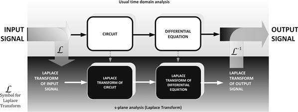
Figure 12.2: Symbolic representation of the procedure for working in the s-plane.
A little more math is useful at this point, as it will aid our understanding of the principles of feedback loop stability later.
Suppose the input signal (in the time domain) is u(t) and the output is v(t), and they are connected by a general second-order differential equation of the type
![]()
It can be shown that if U(s) is the Laplace transform of u(t), and V(s) the transform of v(t), then this equation (in the frequency domain) becomes simply
![]()
So,
![]()
We can therefore define G(s), the transfer function (i.e., output divided by input, now in the s-plane), as
![]()
Therefore,
![]()
Note that this is analogous to the time-domain version of a general transfer function f(t):
![]()
Since the solutions for the general equation G(s) above are well-researched and documented, we can easily compute the response (V) to the stimulus (U).
A power supply designer is usually interested in ensuring that his or her power supply operates in a stable manner over its operating range. To that end, a sine wave is injected at a suitable point in the power supply, and the frequency swept, to study the response. This could be done in the lab and/or “on paper” as we will soon see. In effect, what we are looking at closely is the response of the power supply to any frequency component of a repetitive or nonrepetitive impulse. But in doing so, we are, in effect, only dealing with a steady sine wave stimulus (swept). So, we can then put s=jω (i.e., σ=0).
We can ask — why do we need the complex s-plane at all if we are just going to set s=jω anyway at the end? The answer to that is — we don’t always just do that. For example, we may at some later stage want to compute the exact response of the power supply to a specific disturbance (like a step change in line or load). Then we would need the s-plane and the Laplace transform method. So, even though, we may just end up doing steady-state analysis, by having already characterized the system within the framework of s, we retain the option to be able to conduct a more elaborate analysis of the system response to a more general stimulus if required.
A silver lining for the beleaguered power supply designer is that he or she doesn’t usually even need to know how to actually compute the Laplace transform of a function — unless, for example, the exact step response is required to be computed exactly — like an overshoot or undershoot resulting from a load transient. If the purpose is only to ensure sufficient stability margin is present, steady-state analysis serves the purpose. For that we simply sweep over all possible steady frequencies of input disturbance (either on paper or in the lab), and ensure there is no possibility of ever reinforcing the applied disturbance and making things worse. So, in a full-fledged mathematical analysis, it is convenient to work in the generalized s-plane. At the end, if we just want to calculate the stability margin, we can revert to s=jω. If we want to do more, we have that option too.
Disturbances and the Role of Feedback
In power supplies, we can either change the applied input voltage or increase the load. (This may or may not be done suddenly.) Either way, we always want the output to remain well regulated, and therefore, in effect, to “reject” the disturbance.
But in practice, that clearly does not happen as perfectly as desired. See Figure 12.3 for typical responses of converters to load transients. If instead of load, we suddenly increase the input voltage to a Buck regulator, the output tends to follow suit initially — since D=VIN/VO, and D has not immediately changed. This means, very briefly, VO is proportional to VIN.
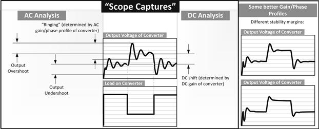
Figure 12.3: Effect of load transients, typical responses and related terms.
To successfully correct the output and perform regulation, the control section of the IC needs to first sense the change in the output, which may take some time. After that it needs to correct the duty cycle, and that also may take some time. Then we have to wait for the inductor and output capacitor to either give up some of their stored energy or to gather some more — whatever is consistent with the conditions required for the new and final steady state. Eventually, the output will hopefully settle down again to its new DC value. We see that there are several such delays in the circuit before we can get the output to stabilize. Minimizing these delays is clearly of great interest. Therefore, for example, just using smaller filter components (L and C) will often help the circuit respond faster.
Note: A philosophical question: how can the control circuit ever know beforehand, how much correction (in duty cycle) to precisely apply (when it senses that the output has shifted from its set value on account of the disturbance)? In fact, it usually doesn’t! It can only be designed to know the general direction to move in, but it does not know beforehand, by how much it needs to move. Hypothetically speaking, we can do several things at our end. For example, we can command the duty cycle to change slowly and progressively, with the output being continuously monitored, and then immediately stop correcting the duty cycle at the very exact moment when the output equals its required regulation level. The duty cycle will thus never exceed the final level it is supposed to be in. However, clearly this is a slow correction process, and so though the duty cycle itself won’t overshoot or undershoot, the output will certainly remain uncorrected for a rather long time. In effect, that amounts to a relative output droop or overshoot, though it is not oscillatory in nature. Another way is to command the duty cycle to change suddenly by a large arbitrary amount (though, of course, in the right direction). However, now the possibility of output overcorrection arises. The output will start getting “corrected” immediately, but because the duty cycle is far in excess of its final steady value, the output will “go the other way,” before the control realizes it. After that, the control does try to correct it again, but it will likely “overreact” again. And so on. In effect, we now get “ringing” at the output. This ringing reflects a basic cause-effect uncertainty that is present in any feedback loop — the control may never fully know for sure whether the error it is seeing on the output is (a) immediate or delayed and (b) whether it is truly an external disturbance, rather than a result of its own attempted correction (coming back to haunt it, in a sense). So, if only after a lot of such avoidable ringing, the output does manage to stabilize, the converter is considered “marginally stable.” In the worst case, this ringing may go on forever, even escalating, before it stabilizes at some constantly oscillating level. In effect, the control loop is now “fully confused,” and the feedback loop is “unstable.”
An “optimum” feedback loop is neither too slow, nor too fast. If it is too slow, the output will exhibit severe overshoot (or undershoot), though the output will not “ring.” If it is too fast (overaggressive), the output will ring severely and even break into full instability (oscillations).
The study of how any disturbance propagates, either getting attenuated, or exacerbated in the process, is called “feedback loop analysis.” In practice, we can test the stability margin of a feedback loop by deliberately injecting a small disturbance at an appropriate point inside it (the “cause”), and then seeing at what magnitude and phase it returns to the same point (the “effect”). If, for example, we find that the disturbance reinforces itself (at the right phase), cause–effect separation will be lost, and instability will result. But if the effect manages to kill or suppress the cause, we will achieve stability.
Note: The use of the word “phase” in the previous paragraph implies we are talking of sine waves once again (there is no such thing as “phase” for a nonsinusoidal waveform). However, this turns out to be a valid assumption because, as we know, arbitrary disturbances can be decomposed into a series of sine wave components of varying frequencies. So, the disturbance/signal we “inject” (either on the bench or on a paper) can be a sine wave of arbitrary amplitude. By sweeping its frequency over a wide range, we can look for frequencies that have the potential to lead to instability. Because one fine day, we may receive a disturbance containing that particular frequency component, and if the margins are insufficient for that frequency, the system will break up into full-blown instability. But if we find that the system has enough margin over a wide range of (sine wave) frequencies, the system would, in effect, be stable when subjected to an arbitrarily shaped disturbance.
A word on the amplitude of the applied disturbances. In this chapter, we are studying only linear systems. That means, if the input to a two-port network doubles, so does the output. Their ratio is therefore unchanged. In fact, that is why the transfer function was never thought of as say, being a function of the amplitude of the incoming signal. But we do know that in reality, if the disturbance is too severe, parts of the control circuit may “rail” — that means, for example, an internal op-amp’s output may momentarily reach very close to its supply rails, thus affording no further correction for some time. We also do realize that there is no perfectly “linear system.” But any system can be approximated by a linear system if the stimulus (and response) is “small” enough. That is why, when we conduct feedback loop analysis of power converters, we talk in terms of “small-signal analysis” and “small-signal models.”
Note: For the same reason, even in bench testing, when injecting a sine wave to characterize the loop response, we must be careful not to apply too high an amplitude. The switching node voltage waveform must therefore be monitored during the test. Too large a jitter in the switching node waveform during the test can indicate possible “railing” (inside the error amplifier circuit). We must also ensure we are not operating close to the “stops” — for example, the minimum or maximum duty cycle limits of the controller and/or the set current limit. But the amplitude of the injected signal must not be too small either, otherwise switching noise is bound to overwhelm the readings (poor signal-to-noise ratio).
Note: For the same reason, most commercial power supply specifications will only ask for a certain transient response for say, from 80% load to max load, or even from 50% to max load, but not from zero to max load.
Transfer Function of the RC Filter, Gain, and the Bode Plot
We know that in general, vo/vi is a complex number called the transfer function. Its magnitude is defined as the “Gain.” Take the simplest case of pure resistors only. For example, suppose we have two 10-k resistors in series and we apply 10 V across both of them. Suppose we define the output as the voltage at the node between the two resistors, we will get 5 V at that point. The transfer function is a real number in this case: 5/10=0.5. So, we can say the gain is 0.5. That is the gain expressed as a pure ratio. We could, however, also express the gain in decibels, as 20×log(|vo/vi|). In our example, that becomes 20×log(0.5)=−6 dB. In other words, gain can be expressed either as 0.5 (a ratio) or in terms of decibels (−6 dB in our case).
Note that by definition, a “decibel” or “dB” is dB=20×log (ratio) — when used to express voltage or current ratios. For power ratios, dB is 10×log (ratio).
Let us now take our simple series RC-network and transform it into the frequency domain, as shown in Figure 12.4. We can discern that the procedure for deriving its transfer function is based on a simple ratio of impedances, now extended to the s-plane.
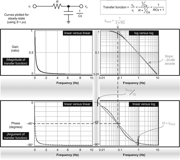
Figure 12.4: Analyzing the first-order low-pass RC filter in the frequency domain.
Thereafter, since we are looking at only steady-state excitations (not transient impulses), we can set s=jω, and plot out (a) the magnitude of the transfer function (i.e., its “gain”) and (b) the argument of the transfer function (i.e., its phase) — both in the frequency domain of course. This combined gain-phase plot is called a “Bode plot.”
A word on terminology: Note that initially, we will denote the ratio |vo/vi| as “Gain,” and we will distinguish it from 20×log(|vo/vi|) by calling the latter “GaindB.” But these terms are actually often used interchangeably in literature and later in this chapter too. It can get confusing, but with a little experience it should quickly become obvious what is being meant in any particular context. Usually, however, “Gain” is used to refer to its dB version, that is, 20×log (|vo/vi|).
Note that gain and phase are defined only in steady state as they implicitly refer to a sine wave (“phase” has no meaning otherwise!).
Here are a few observations based on Figure 12.4:
• We have converted the phase angle (which was originally in radians, θ=ωt) into degrees. That is because many engineers feel more comfortable visualizing angle in degrees instead of radians. To this end, we have used the following conversion: degrees=(180/π)×radians.
• Gain (on the vertical axis) is a simple ratio (not in decibels, unless stated otherwise).
• We have similarly converted from “angular frequency” (ω in radians/second) to the usual frequency (in Hz). Here we have used the equation: Hz=(radians/second)/(2π).
• By varying the type of scaling on the gain and phase plots, we can see that the gain becomes a straight line if we use log versus log scaling. Note that in Figure 12.1, we had to use log versus linear scaling to get that curve to look like a straight line.
• We will get a straight-line gain plot in either of the two following cases — (a) if the gain is expressed as a simple ratio (i.e., Vout/Vin), and plotted on a log scale (on the y-axis) or (b) if the gain is expressed in decibels (i.e., 20×log Vout/Vin), and we use a linear scale to plot it. Note that in both cases, on the x-axis, we can either use “f” (frequency) and plot it using a log scale, or take 20×log(f) upfront, and plot it on a linear scale.
• In plotting logs, we must remember that the log of 0 is impossible to plot (log 0→−∞), and so we must not let the origin of a log scale ever be 0. We can set it close to zero, say 0.0001, or 0.001, or 0.01, and so on, but certainly not 0.
• We thus confirm by looking at the curves in Figure 12.4 that the gain at high frequencies starts decreasing by a factor of 10 for every 10-fold increase in frequency. Note that by the definition of decibel, a 10:1 voltage ratio is 20 dB (check 20 log(10)=20). Therefore, we can say that the gain falls at the rate of −20 dB per decade at higher frequencies. A circuit with a slope of this magnitude is called a “first-order filter” (in this case a low-pass one).
• Further, since this slope is constant, the signal must also decrease by a factor of 2 for every doubling of frequency. Or by a factor of 4 for every quadrupling of frequency, and so on. But a 2:1 ratio is 6 dB, and an “octave” is a doubling (or halving) of frequency. Therefore, we can also say that the gain of a low-pass first-order filter falls at the rate of −6 dB per octave (at high frequencies).
• If the x and y scales are scaled and proportioned identically, the actual angle the gain plot will make with the x-axis is −45°. The slope, that is, tangent of this angle is then tan(−45°)=−1. Therefore, a slope of −20 dB/decade (or −6 dB/octave) is often simply called a “−1” slope.
• Similarly, when we have filters with two reactive components (i.e., an inductor and a capacitor), we will find the slope is −40 dB/decade (i.e., −12 dB/octave). This is usually called a “−2” slope (the actual angle being about −63° when the axes are proportioned and scaled identically).
• The bold gray straight lines in the right-hand side graphs of Figure 12.4 form the “asymptotic approximation.” We see that the gain asymptotes have a “break frequency” or “corner frequency” at f=1/(2πRC). This point can also be referred to as the “resonant frequency” of the RC filter, or a “pole” as discussed later.
• Note that the error/deviation between the actual curve and its asymptotic approximation is usually very small (only for first-order filters, as discussed later). For example, the worst-case error for the gain of the simple RC-network in Figure 12.4 is only −3 dB, and that occurs at the break frequency. Therefore, the asymptotic approximation is a valid “shortcut” that we will often use from now on to simplify the plots and their analysis.
• With regard to the asymptotes of the phase plot, we see that we get two break frequencies for it — one at one-tenth, and the other at 10 times the break frequency of the gain plot. The change in the phase angle at each of these break-points is 45° — giving a total phase shift of 90°. It spans two decades (symmetrically around the break frequency of the gain plot).
• Note that at the magnitude of the frequency where the single-pole lies, the phase shift (measured from the origin) is always 45° — that is, half the overall shift — whether we are using the asymptotic approximation or the actual curve.
• Since both the gain and the phase fall as frequency increases, we say we have a “pole” present. In our case, the pole is at the break frequency of 1/(2πRC). It is also called a “single-pole” or a first-order pole, since it is associated with a −1 slope.
• Later, we will see that similar to a “pole,” we can also have a “zero,” which is identifiable by the fact that both the gain and the phase start to rise with frequency from that location.
• In Figure 12.4, we see that the output voltage is clearly always less than the input voltage —that is, true for a (passive) RC-network (not involving op-amps yet). In other words, the gain is less than 1 (0 dB) at any frequency. Intuitively, that seems right because there seems to be no way to “amplify” a signal, without using an active device like an op-amp or transistor for example. However, as we will soon see, if we use passive filters involving both types of reactive components (L and C), we can in fact get the output voltage to exceed the input at certain frequencies. We then have “second-order” filters. And their response is what we more commonly refer to as “resonance.”
The Integrator Op-amp (“Pole-at-Zero” Filter)
Before we go on to passive networks involving two reactive components, let us look at an interesting active RC-based (first-order) filter. The one chosen for discussion here is the “integrator” because it happens to be the fundamental building block of any “compensation network.”
The inverting op-amp presented in Figure 12.5 has only a capacitor present in its feedback path. We know that under steady DC conditions, all capacitors essentially “go out of the picture.” In our case, we are therefore left with no negative feedback at all at DC — and therefore infinite DC gain (though in practice, real op-amps will limit this to a very high, but finite value). But more surprisingly perhaps, that does not stop us from knowing the precise gain at higher frequencies. If we calculate the transfer function of this circuit, we will see that something “special” once again happens at the point f=1/(2π×RC). However, unlike the passive RC filter, this point is not a break-point, nor a pole or zero location. It happens to be the point where the gain is unity (0 dB). We will denote this frequency as “fp0.”
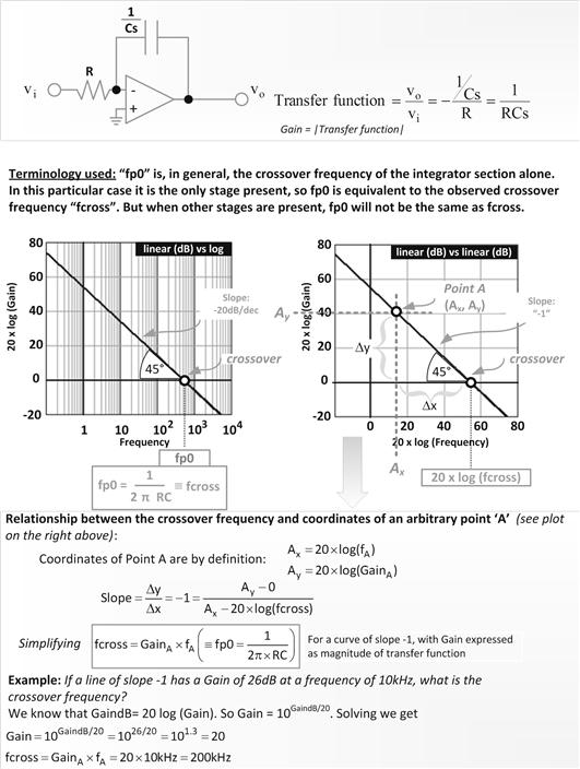
Figure 12.5: The integrator (pole-at-zero) operational amplifier and some related math.
Note that so far, as indicated in Figure 12.5, the integrator is the only stage present. So, in this particular case, “fp0” is the same as the observed crossover frequency “fcross.” But in general, that will not be so. In general, in this chapter, “fp0” will refer to the crossover frequency the integrator stage would have produced were it present alone.
Note that the integrator has a single-pole at “zero frequency,” though 0 cannot be displayed on a log scale. We always strive to introduce this pole-at-zero because without it, the system would have rather poor DC (low-frequency) gain. The integrator is the simplest way to try to get as high a DC gain as possible. Having a high DC gain is the way to achieve good steady-state regulation in any power converter. This is indicated in Figure 12.3 too (labeled the “DC shift”). A high DC gain will reduce the DC shift.
On the right side of Figure 12.4, we have deliberately made the graph geometrically square in shape. To that end, we have assigned an equal number of grid divisions on the two axes, that is, the axes are scaled and proportioned identically. In addition, we have plotted 20×log(f) on the y-axis (instead of just log(f)). Having thus made the x- and y-axes identical in all respects, we realize why the slope is called “−1” — it really does fall at exactly 45° (now we see that visually too).
We take this opportunity to show how to do some simple math in the log-plane. This is shown in the lower part of Figure 12.5. We have derived one particular useful relationship between an arbitrary point “A” and the crossover frequency “fcross.” A numerical example is also included.
![]()
Note that, in general, the transfer function of any “pole-at-zero” function will always have the following form (X being a general real number)
![]()
The crossover frequency is then
![]()
Mathematics in the Log-Plane
As we proceed toward our ultimate objective of control loop analysis and compensation network design, we will be multiplying transfer functions of cascaded blocks to get the overall transfer function. That is because the output of one block forms the input for the next block, and so on. It turns out that the mathematics of gain and phase is actually much easier to perform in the log-plane rather than in a linear plane. The most obvious reason for that is log(AB)=log A+log B. So, we can add rather than multiply if we use logs. We have already had a taste of this in Figure 12.5. Let us summarize some simple rules that will help us later.
(a) If we take the product of two transfer functions A and B (cascaded stages), we know that the combined transfer function is the product of each:
![]()
But we also know that log(C)=log(AB)=log(A)+log(B). In words, the gain of A in decibels plus the gain of B in decibels gives us the combined gain (C) in decibels. So, when we combine transfer functions, since decibels add up, that route is easier than taking the product of various transfer functions.
(b) The overall phase shift is the sum of the phase shifts produced by each of the cascaded stages. So, phase angles simply add up numerically (even in the log-plane).
(c) In Figure 12.6, we are using the term GaindB (the Gain expressed in dB), that is, 20 log (Gain), where Gain is the magnitude of the transfer function.
(d) From the upper half of Figure 12.6, we see that if we know the crossover frequency (and the slope of the line), we can find the gain at any frequency.
(e) Suppose we now shift the plotted line vertically (keeping the slope constant) as shown in the lower half of Figure 12.6. Then, by the equation provided therein, we can calculate by what amount the crossover frequency shifts in the process. Or equivalently, if we shift the crossover frequency by a known amount, we can calculate what will be the impact on the DC gain — because we will know by how much the curve has shifted either up or down in decibels.
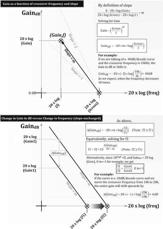
Figure 12.6: Some more math in the log-plane.
Transfer Function of the Post-LC Filter
Moving toward power converters, we note that in a Buck, there is a post-LC filter present. Therefore, its filter stage can be treated as a simple “cascaded stage” immediately following the switch. The overall transfer function is very easy to compute as per the rules mentioned in the previous section (a product of cascaded transfer functions). However, when we come to the Boost and Buck-Boost, we don’t have a post-LC filter — because there is a switch/diode connected between the two reactive components. However, it can be shown that even the Boost and Buck-Boost can be manipulated into a “canonical model” in which an effective post-LC filter appears at the output (like a Buck) — thus making them as easy to treat as a Buck (i.e., cascaded stages). The only difference is that in this canonical model, the actual inductance L (of the Boost and Buck-Boost) gets replaced by an equivalent (or effective) inductance equal to L/(1−D)2. The capacitor (the C of the LC) remains the same in the canonical model.
Since the simple LC post-filter now becomes representative of the output section of any typical switching topology, we need to understand it better as shown in Figure 12.7.
• For most practical purposes, we can assume that the break frequency (indicated in Figure 12.7) does not depend on the load or on any associated parasitic resistive elements of the components. In other words, the resonant frequency of the filter-plus-load combination (the break frequency, or “pole” in this case) can be taken to be simply 1/(2π√(LC), that is, no resistance term is included.
• The LC-filter gain decreases at the rate of “−2” at high frequencies. The phase also decreases providing a total phase shift of 180°. So, we say we have a “double-pole” (or second-order pole) at the break frequency 2π√(LC).
• Q is the “quality factor” (as defined in the figure). In effect, it quantifies the amount of “peaking” in the response curve at the break frequency point. Very simply put, if, for example, Q=20, then the output voltage at the resonant frequency is 20 times the input voltage. On a log scale, this is written as 20×log Q, as shown in the figure. If Q is very high, the filter is considered “under-damped.” If Q is very small, the filter is “over-damped.” And if Q =0.707, we have “critical damping.” In critical damping, the gain at the resonant frequency is 3 dB below its DC value, that is, the output is 3 db below the input (similar to an RC filter). Note that −3 dB is a factor of 1/√2=0.707, that is, roughly 30% lower. Similarly, +3 dB is √2=1.414 (i.e., roughly 40% higher).
• As indicated, the effect of resistance on the break frequency is usually minor, and therefore ignored. But the effect of resistance on Q (i.e., on the peaking) is significant (though eventually, that may be ignored too). However, we should keep in mind that the higher the associated series parasitic resistances of L and C, the lower is the Q. On the other hand, if we reduce the load, that is, increase the resistance across the C, Q increases. Remember that a high parallel resistance is in effect a small series resistance, and vice versa. In general, the presence of any significantly large series resistance ends up reducing Q, and any significantly small parallel resistance does just the same.
• As in Figure 12.4, we can use the “asymptotic approximation” for the LC gain plot too. However, the problem with trying to do the same with the phase of the LC is that there can now be a very large error — more so if Q becomes very large. Because if Q is very large, we can get a very abrupt phase shift (full 180°) in the region very close to the resonant frequency — not spread out smoothly over one-tenth to 10 times the break frequency as in Figure 12.4. This sudden phase shift can, in fact, become a real problem in a power supply, since it can induce “conditional stability” (discussed later). Therefore, a certain amount of damping helps from the standpoint of “phase-shift softening,” thereby avoiding any possible conditional stability tendencies.
• Unlike an RC filter, the output voltage can in this case be greater than the input voltage (around the break frequency). But for that to happen, Q must be greater than 1.
• Instead of using Q, engineers often prefer to talk in terms of the “damping factor,” defined as
![]()
So a high Q corresponds to a low ζ.
From the equations for Q and resonant frequency, we can conclude that if L is increased, Q tends to decrease, and if C is increased, Q increases.
Note: One of the possible pitfalls of putting too much output capacitance in a power supply is that we may be creating significant peaking (high Q) in its output filter’s response. And we know that when that happens, the phase shift is also more abrupt, and that can induce conditional instability. So generally, if we increase C but simultaneously increase L, we can keep the Q (and the peaking) unchanged. But the break frequency changes significantly and that may not be acceptable.
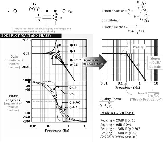
Figure 12.7: The LC filter analyzed in the frequency domain.
Summary of Transfer Functions of Passive Filters
The first-order (RC) low-pass filter transfer function (Figure 12.4) can be written in several different ways:
![]()
![]()
![]()
where ωO=1/(RC). Note that the “K” in the last equation above is a constant multiplier often used by engineers who are more actively involved in the design of filters. And in this case, K=ω0.
For the second-order filter (Figure 12.7), various equivalent forms seen in literature are
![]()
![]()
![]()
![]()
where ω0=1/(LC)1/2. Note that here, K=ω02. Also, Q is the quality factor, and ζ is the damping factor defined earlier.
Finally, note also, that the following two relations are very useful when trying to manipulate the transfer function of the LC-filter into different forms
![]()
Poles and Zeros
Let us try to “connect the dots” now. We had mentioned in the case of both the first- and the second-order filters (Figures 12.4 and 12.7) that something called a “pole” exists. We should recognize that we got poles in both cases only because both the first- and the second-order transfer functions had terms in “s” in the denominators of their respective transfer functions. So, if s takes on specific values, it can force the denominator to become zero, and the transfer function (in the complex plane) then becomes “infinite.” That is actually the point where we get a “pole” by definition. Poles occur wherever the denominator of the transfer function becomes zero. In general, the values of s at which the denominator becomes zero (i.e., the location of the poles) are sometimes called “resonant frequencies.” For example, a hypothetical transfer function “1/s” will give us a pole at zero frequency (the “pole-at-zero” we talked about in the integrator shown in Figure 12.5).
Note that the gain, which is the magnitude of the transfer function (calculated by putting s=jω), won’t necessarily be really “infinite” at the pole location as stated rather intuitively above. For example, in the case of the RC filter, we know that the gain is in fact always less than, or equal to unity, despite a pole being present at the break frequency.
Note that if we interchange the positions of the two primary components of each of the passive low-pass filters we discussed earlier, we will get the corresponding “high-pass” RC and LC-filters, respectively. If we calculate their transfer functions in the usual manner, we will see that besides giving us poles, we also now get single- and double-zeros respectively as indicated in Figure 12.8. Zeros occur wherever the numerator of the transfer function becomes zero. Note that in Figure 12.8, the zeros are not visible, only the poles are. But the presence of the zeros is indicated by the fact that we started from the left of each graph with curves rising upward (rather than being flat with frequency), and for the same reason, the phase started off with 90° for the first-order filter and from 180° for the second-order filter, rather than from 0°.
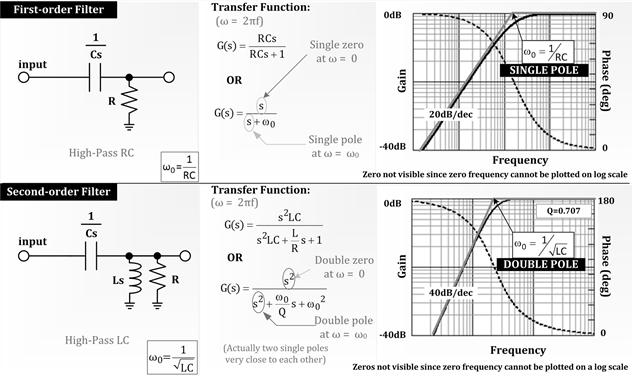
Figure 12.8: High-pass RC and LC (first-order and second-order) filters.
We had mentioned that gain-phase plots are called Bode plots. In the case of Figure 12.8, we have drawn these on the same graph just for convenience. Here the solid line is the gain, and to read its value, we need to look at the y-axis on the left side of the graph. Similarly, the dashed line is the phase, and for it, we need to look at the y-axis on the right side. Note that for practice, we have reverted to plotting the gain as a simple ratio (not in decibels), but we are now plotting that on a log scale. The reader should hopefully, by now, have learnt to correlate the major grid divisions of this type of plot with the corresponding dB. So a 10-fold increase is equivalent to +20 dB, a 100-fold increase is +40 dB, and so on.
We can now generalize our approach. A network transfer function can be described as a ratio of two polynomials:
![]()
This can be factored out as
![]()
So, the zeros (i.e., leading to the numerator being zero) occur at the complex frequencies s=z1, z2, z3, …. The poles (denominator zero) occur at s=p1, p2, p3, …
In power supplies, we usually deal with transfer functions of the form:
![]()
So the “well-behaved” poles and zeros that we have been talking about are actually in the left-half of the complex-frequency plane (“LHP” poles and zeros). Their locations are at s=−z1, −z2, −z3, −p1, −p2, −p3, …. We can also, in theory, have right-half plane poles and zeros which have very different behavior to normal poles and zeros, and can cause almost intractable instability. This aspect is discussed later.
“Interactions” of Poles and Zeros
We will learn that in trying to find the overall transfer function of a converter, we typically add up several of its constituent transfer functions together. As mentioned, the math is easier to do on a log-plane if we are dealing with cascaded stages. The equivalent post-LC filter, which we studied in Figure 12.7, is one of those cascaded stages. However, for now we will still keep things general here, and simply show how to add up several transfer functions together in the log-plane. We just have several poles and zeros, and we must know how to add these up too.
We can break up the full analysis in two parts:
(a) For poles and zeros lying along the same gain plot (i.e., belonging to the same transfer function/stage) — the effect is cumulative in going from left to right. So, suppose we are starting from zero frequency and move right toward a higher frequency, and we first encounter a double-pole. We know that the gain will start falling with a slope of −2 beyond the corresponding break frequency. As we go further to the right, suppose we now encounter a single-zero. This will impart a change in slope of +1. So the net slope of the gain plot will now become −2+1=−1, after the zero location. Note that despite a zero being present, the gain is still falling, though at a lesser rate. In effect, the single-zero canceled half the double-pole, so we are left with the response of a single-pole (to the right of the zero).
The phase angle also cumulates in a similar manner, except that in practice a phase angle plot is harder to analyze. That is because phase shift can take place slowly over two decades around the resonant frequency. We also know that for a double-pole (or double-zero), the change in phase may in fact be very abrupt at the resonant frequency. However, eventually, a good distance away in terms of frequency, the net effect is still predictable. So, for example, the phase angle plot of a double-pole, followed shortly by a single-zero, will start with a phase angle of 0° (at DC) which will then decrease gradually toward −180° on account of the double-pole. But about a decade below the location of the single-zero, the phase angle will then gradually start increasing (though still remaining negative). It will eventually settle down to −180°+90°=−90° at high frequencies, consistent with a single net pole.
(b) For poles and zeros lying along different gain plots (belonging to say several cascaded stages that are being summed up) — we know that the overall gain in decibels is the sum of the gain of each (also in decibels). The effect of this math on the pole-zero interactions is therefore simple to describe. If, for example, at a specific frequency, we have a double-pole in one plot and a single-zero on the other plot, then the overall (combined) gain plot will have a single-pole at this break frequency. So, we see that poles and zeros tend to “destroy” (cancel) each other out. Zeros are considered to be “anti-poles” in that sense. But poles and zeros also add up with their own type. For example, if we have a double-pole on one plot, and a single-pole on the other plot (at the same frequency), the net gain (on the composite transfer function plot) will change slope by “−3” after this frequency. Phase angles also add up similarly. A few examples later will make this much clearer.
Closed and Open-Loop Gain
Figure 12.9 represents a general feedback controlled system. The “plant” (also sometimes called the “modulator”) has a “forward transfer function” G(s). A part of the output gets fed back through the feedback block, to the control input, so as to produce regulation at the output. Along the way, the feedback signal is compared with a reference level, which tells it what the desired level is for it to regulate to.
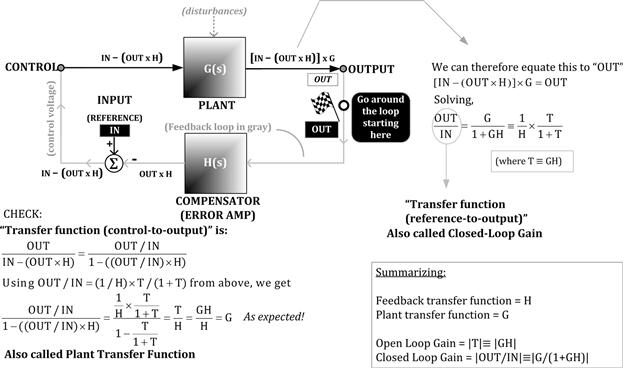
Figure 12.9: General feedback loop analysis.
H(s) is the “feedback transfer function,” and we can see this goes to a summing block (or node) — represented by the circle with an enclosed summation sign.
Note: The summing block is sometimes shown in literature as just a simple circle (nothing enclosed), but sometimes rather confusingly as a circle with a multiplication sign (or x) inside it. Nevertheless, it still is a summation block.
One of the inputs to this summation block is the reference level (the “input” from the viewpoint of the control system), and the other is the output of the feedback block (i.e., the part of the output being fed back). The output of the summation node is the “error” signal.
Comparing Figure 12.9 with Figure 12.10, we see that in a power supply, the plant itself can be split into several cascaded blocks. These blocks are — the PWM (not to be confused with the term “modulator” often used in general control loop theory referring to the entire plant), the power stage consisting of the driver-plus-switch, and the LC-filter. The feedback block, on the other hand, consists of the voltage divider (if present) and the compensating error amplifier. Note that we may prefer to visualize the error amplifier block as two cascaded stages — one that just computes the error (summation node) and another which accounts for the gain (and its associated compensation network). But in actual practice, since we apply the feedback signal to the inverting pin of the error amplifier, both functions are combined. Also note that the basic principle behind the PWM stage (which determines the duty cycle of the pulses driving the switch) is explained in the next section and in Figure 12.11.
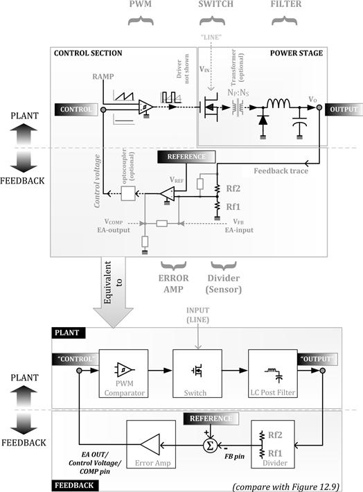
Figure 12.10: A power converter: its plant and feedback (compensator) blocks.
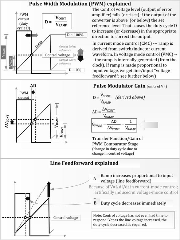
Figure 12.11: PWM action, transfer function, and line feedforward explained.
In general, the plant can receive various “disturbances” that can affect its output. In a power supply, these are essentially the line and load variations. The basic purpose of feedback is to reduce the effect of these disturbances on the output voltage (see Figure 12.3, for example).
Note that the word “input” in control loop theory is not the physical input power terminal of the converter. Its location is actually marked in Figure 12.9. It happens to be the reference level we are setting the output to. The word “output” in control loop theory, however, is the same as the physical output terminal of the converter.
In Figure 12.9, we have derived the open-loop gain |T|=|GH|, which is simply the magnitude of the product of the forward and feedback transfer functions, that is, obtained by going around the loop fully once. On the other hand, the magnitude of the reference-to-output (i.e., input-to-output) transfer function is called the closed-loop gain. It is |G/(1+GH)|.
Note that the word “closed” has really nothing to do with the feedback loop being literally “open” or “closed” as sometimes thought. Similarly, “GH” is called the “open-loop transfer function” — irrespective of whether the loop is literally “open,” say for the purpose of measurement, or “closed” as in normal operation. In fact, in a typical power supply, we can’t even hope to break the feedback path for the purpose of any measurement. Because the gain is typically so high that even a minute change in the feedback voltage will cause the output to swing wildly. So, in fact, we always need to “close” the loop and thereby DC-bias the converter into full regulation, before we can even measure the so-called “open-loop” gain.
The Voltage Divider
Usually, the output VO of the power supply first goes to a voltage divider. Here it is, in effect, just stepped-down, for subsequent comparison with the reference voltage “VREF.” The comparison takes place at the input of the error amplifier, which is usually just a conventional op-amp (voltage amplifier).
We can visualize an ideal op-amp as a device that varies its output so as to virtually equalize the voltages at its input pins. Therefore, in steady state, the voltage at the node connecting Rf2 and Rf1 (see “divider” block in Figure 12.10) can be assumed to be (almost) equal to VREF. Assuming that no current flows out of (or into) the divider at this node, using Ohm’s law:
![]()
Simplifying,
![]()
So this tells us what ratio of the voltage divider resistors we must have to produce the desired output rail.
Note, however, that in applying control loop theory to power supplies, we are actually looking only at changes (or perturbations), not the DC values (though this was not made obvious in Figure 12.9). It can also be shown that when the error amplifier is a conventional op-amp, the lower resistor of the divider Rf1 behaves only as a DC biasing resistor and does play any (direct) part in the AC loop analysis.
Note: The lower resistor of the divider Rf1 does not enter the AC analysis, provided we are considering ideal op-amps. In practice, it does affect the bandwidth of a real op-amp, and therefore may on occasion need to be considered.
Note: If we are using a spreadsheet, we will find that changing Rf1 in a standard op-amp-based error amplifier divider does, in fact, affect the overall loop. But we should be clear that that is only because by changing Rf1, we have changed the duty cycle of the converter (via its output voltage), which thus affects the plant transfer function. Therefore, the effect of Rf1 is indirect. Rf1 does not enter into any of the equations that tell us the locations of the poles and zeros of the system.
Note: We will see that when using a transconductance op-amp as the error amplifier, Rf1 does enter the AC analysis.
Pulse-Width Modulator Transfer Function
The output of the error amplifier (sometimes called “COMP,” sometimes “EA-out,” sometimes “control voltage”) is applied to one of the inputs of the PWM comparator. This is the terminal marked “Control” in Figures 12.9 and 12.10. On the other input of this PWM comparator, we apply a sawtooth voltage ramp — either internally generated from the clock when using “voltage-mode control,” or derived from the current ramp when using “current-mode control” (explained later). Thereafter, by standard comparator action, we get pulses of desired width with which to drive the switch.
Since the feedback signal coming from the output rail of the power supply goes to the inverting input of the error amplifier, if the output is below the set regulation level, the output of the error amplifier goes high. This causes the PWM to increase the pulse width (duty cycle) and thus try to make the output voltage rise. Similarly, if the output of the power supply goes above its set value, the error amplifier output goes low, causing the duty cycle to decrease (see upper third of Figure 12.11).
As mentioned previously, the output of the PWM stage is duty cycle, and its input is the “control voltage” or the “EA-out.” So, as we said, the gain of this stage is not a dimensionless quantity, but has units of 1/V. From the middle of Figure 12.11, we can see that this gain is equal to 1/VRAMP, where VRAMP is the peak-to-peak amplitude of the ramp sawtooth.
Voltage (Line) Feedforward
We had also mentioned previously that when there is a disturbance, the control does not usually know beforehand how much duty cycle correction to apply. However, in the lowermost part of Figure 12.11, we have described an increasingly popular technique being used to make that a reality, at least when faced with line disturbances. This is called input-voltage/line feedforward, or simply “feedforward.”
This technique requires the input voltage be sensed and the slope of the comparator sawtooth ramp increased if the input goes up. In the simplest implementation, a doubling of the input causes the slope of the ramp to double. Then, from Figure 12.11, we see that if the slope doubles, the duty cycle is immediately halved. In a Buck, the governing equation is D=VO/VIN. So, if a doubling of input occurs, we know that naturally, the duty cycle will eventually halve anyway. So, rather than wait for the control voltage to decrease by half to lower the duty cycle (keeping the ramp unchanged), we could also change the ramp itself — in this case, double the slope of the ramp and thereby achieve the very same result (i.e., halving of duty cycle) almost instantaneously.
Summarizing: the duty cycle correction afforded by this “automatic” ramp correction is exactly what is required for a Buck, since its duty cycle D=VO/VIN. More importantly, this correction is virtually instantaneous — we didn’t have to wait for the error amplifier to detect the error on the output (through the inherent delays of its RC-based compensation network scheme), and respond by altering the control voltage. So, in effect, by input/line feedforward, we have bypassed all major delays, and therefore line correction is almost immediate — and that amounts to almost “perfect” rejection of the line disturbance.
In Figure 12.11, it is implied that the PWM ramp is created artificially from the fixed internal clock. That is called voltage-mode control. In current-mode control, the PWM ramp is basically an appropriately amplified version of the switch/inductor current. We will discuss that in more detail later. Here we just want to point out that the line feedforward technique described in Figure 12.11 is applicable only to voltage-mode control. However, the original inspiration behind the idea does come from current-mode control — in which the PWM ramp, generated from the inductor current, automatically increases if the line voltage increases. That partly explains why current-mode control seems to respond so much “faster” to line disturbances than traditional voltage-mode control and one of its oft-repeated advantages.
However, one question remains: how good is the “built-in” automatic line feedforward in current-mode control? In a Buck topology, the slope of the inductor current up-ramp is equal to (VIN−VO)/L. So, if we double the input voltage, we do not end up doubling the slope of the inductor current. Therefore, neither do we end up automatically halving the duty cycle, as we can do easily in line feedforward applied to voltage-mode control.
In other words, voltage-mode control with proportional line feedforward control, though inspired by current-mode control, provides better line rejection than current-mode control (for a Buck). Voltage-mode control with line feedforward is considered by many to be a far better choice than current-mode control, all things considered.
Power Stage Transfer Function
As per Figure 12.10, the “power stage” formally consists of the switch plus the (equivalent) LC-filter. Note that this is just the plant minus the PWM. Alternatively stated, if we add the PWM comparator section to the power stage, we get the “plant” as per control loop theory, and that was symbolized by the transfer function “G” in Figure 12.9. The rest of the circuit in Figure 12.10 is the feedback block, and this was symbolized by the transfer function H in Figure 12.9.
We had indicated previously that whereas in a Buck, the L and C are really connected to each other at the output (as drawn in Figure 12.10), in the remaining two topologies they are not. However, the small-signal (canonical) model technique can be used to transform these latter topologies into equivalent AC models — in which, for all practical purposes, a regular LC-filter does appear after the switch, just as for a Buck. With this technique, we can then justifiably separate the power stage into a cascade of two separate stages (as for a Buck):
• A stage that effectively converts the duty cycle input (coming from the output of the PWM stage) into an output voltage.
• An equivalent post-LC filter stage that takes in this output and converts it into the output rail of the converter.
With this understanding, we can finally build the final transfer functions presented in the next section.
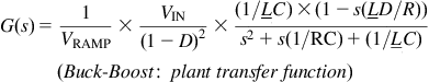
Plant Transfer Functions of All the Topologies
Let us discuss the three topologies separately here. Note that we are assuming voltage-mode control and continuous conduction mode (CCM). Further, the “ESR (effective series resistance) zero” is not included here (a simple modification introduced later).
(a) Control-to-output transfer (plant) function
The transfer function of the plant is also called the “control-to-output transfer function” (see Figure 12.10). It is the output voltage of the converter, divided by the “control voltage” (i.e., the output of the error amplifier, or “EA-out”). We are, of course, talking only from an AC point of view, and are therefore interested only in the changes from the DC-bias levels.
The control-to-output transfer function is a product of the transfer functions of the PWM modulator, the switch and the LC-filter (since these are cascaded stages). Alternatively, the control-to-output transfer function is a product of the transfer function of the PWM comparator and the transfer function of the “power stage.”
We already know from Figure 12.11 that the transfer function of the PWM stage is equal to the reciprocal of the amplitude of the ramp. And as discussed in the previous section, the power stage itself is a cascade of an equivalent post-LC stage (whose transfer function is the same as the passive low-pass second-order LC filter we discussed previously in Figure 12.7), plus a power stage that finally converts the duty cycle into a DC output voltage VO.
We are now interested in finding the transfer function of the latter stage referred to above.
The overall question is — what happens to the output when we perturb the duty cycle slightly (keeping the input to the converter VIN constant). Here are the steps for a Buck
![]()
![]()
So, in very simple terms, the required transfer function of the intermediate “duty cycle-to-output stage” is equal to VIN for a Buck.
Finally, the control-to-output (plant) transfer function is the product of three (cascaded) transfer functions, that is, it becomes
![]()
Alternatively, this can be written as
![]()
where ω0=1/√(LC) and ω0Q=R/L.
(b) Line-to-output transfer function
Of great importance in any converter design is not what happens to the output when we perturb the reference (which is what the closed-loop transfer function really is), but what happens at the output when there is a line disturbance. This is often referred to as “audio susceptibility” (probably because early converters switching at around 20 kHz would emit audible noise under this condition).
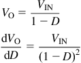
The equation connecting the input and output voltages is simply the DC input-to-output transfer function, that is,
![]()
So, D is also the factor by which the input line (VIN) disturbance gets scaled, and thereafter applied at the input of the equivalent LC post-filter for further attenuation as per Figure 12.7. We already know the transfer function of the LC low-pass filter. Therefore, the line-to-output transfer function is the product of the two cascaded transfer functions, that is,
![]()
where R is the load resistor (at the output of the converter).
Alternatively, this can be written as
![]()
where ω0=1/√(LC), and ω0Q=R/L.
(a) Control-to-output (plant) transfer function
Proceeding similar to the Buck, the steps for this topology are
So the control-to-output transfer function is a product of three transfer functions:
![]()
where L=L/(1−D)2. Note that this is the inductor in the “equivalent post-LC filter” of the canonical model. Also note that C remains unchanged.
Alternatively, the above transfer function can be written as
![]()
where ω0=1/√(LC) and ω0Q=R/L.
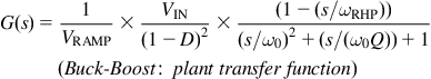
Note that we have included a surprise term in the numerator above. By detailed modeling, it can be shown that both the Boost and the Buck-Boost have such a term. This term represents a zero, but a different type to the “well-behaved” zero discussed so far (note the sign in front of the s-term is negative, so it occurs in the positive, i.e., the right-half portion of the s-plane). If we consider its contribution to the gain-phase plot, we will find that as we raise the frequency, the gain will increase (as for a normal zero), but simultaneously, the phase angle will decrease (opposite to a “normal” zero, more like a “well-behaved” pole).
Why is that a problem? Because, later we will see that if the overall open-loop phase angle drops sufficiently low, the converter can become unstable. That is why this zero is considered undesirable. Unfortunately, it is virtually impossible to compensate for (or “kill”) by normal techniques. The usual method is to literally “push it out” — to higher frequencies where it can’t affect the overall loop significantly. Equivalently, we need to reduce the bandwidth of the open-loop gain plot to a frequency low enough that it just doesn’t “see” this zero. In other words, the crossover frequency must be set much lower than the location of the RHP zero.
The name given to this zero is the “RHP zero,” as indicated earlier — to distinguish it from the “well-behaved” (conventional) left-half-plane zero. For the Boost topology, its location can be found by setting the numerator of the transfer function above (see its first form) to zero, that is, s×(L/R)=1. So, the frequency location of the Boost RHP zero is
![]()
Note that the very existence of the RHP zero in the Boost and Buck-Boost can be traced back to the fact that these are the only topologies where an actual LC post-filter doesn’t exist on the output. Though, by using the canonical modeling technique, we have managed to create an effective LC post-filter, the fact that in reality there is a switch/diode connected between the actual L and C of the topology is what is ultimately responsible for creating the RHP zero.
Note: The RHP zero is often explained intuitively as follows — if we suddenly increase the load, the output dips slightly. This causes the converter to increase its duty cycle in an effort to restore the output. Unfortunately, for both the Boost and the Buck-Boost, energy is delivered to the load only during the switch off-time. So, an increase in the duty cycle decreases the off-time, and there is now, unfortunately, a smaller interval available for the stored inductor energy to get transferred to the output. Therefore, the output voltage, instead of increasing as we were hoping, dips even further for a few cycles. This is the RHP zero in action. Eventually, the current in the inductor does manage to ramp up over several successive switching cycles to the new level consistent with the increased energy demand, and so this strange situation gets corrected — provided full instability has not already occurred!
The RHP zero can occur at any duty cycle. Note that its location is at a lower frequency as D approaches 1 (i.e., at lower input voltages). It also moves to a lower frequency if L is increased. That is one reason why bigger inductances are not preferred in Boost and Buck-Boost topologies.
(b) Line-to-output transfer function
We know that
![]()
![]()
Alternatively, this can be written as
![]()
where ω0=1/√(LC) and ω0Q=R/L.
(a) Control-to-output transfer (plant) function
Here are the steps for this topology:
(Yes, it is an interesting coincidence — the slope of 1/(1−D) calculated for the Boost is the same as the slope of D/(1−D) calculated for the Buck-Boost!)
So, the control-to-output transfer function is
where L=L/(1−D)2 is the inductor in the equivalent post-LC filter.
Alternatively, this can be written as
where ω0=1/√(LC) and ω0Q=R/L.
Note that, as for the Boost, we have included the RHP zero term in the numerator (in gray). Its location is similarly calculated to be
![]()
This also comes in at a lower frequency if D approaches 1 (lower input). Compare with what we got for the Boost:
![]()
(b) Line-to-output transfer function
We know that
![]()
![]()
This is alternatively written as
![]()
where ω0=1/√(LC) and ω0Q=R/L.
Note that the plant and line transfer functions of all the topologies calculated above do not depend on the load current IO. That is why gain-phase plots (Bode plots) do not change much if we vary the load current (provided we stay in CCM as assumed above).
Note also that so far we have ignored a key element of the transfer functions — the ESR of the output capacitor and its contribution to the “ESR–zero.”
Whereas the DCR (DC resistance) usually just ends up decreasing the overall Q (less “peaky” at the second-order (LC) resonance), the ESR actually contributes a zero to the open-loop transfer function. And because it affects the gain and the phase significantly, it usually can’t be ignored — certainly not if it lies below the crossover frequency (i.e., at a lower frequency). We will account for it later by just canceling it out with a pole.
Feedback-Stage Transfer Functions
We can now lump the entire feedback section, including the voltage divider, error amplifier, and the compensation network. However, depending on the type of error amplifier used, these must be evaluated rather differently. In Figure 12.12, we have shown two possible error amplifiers often used in power converters.
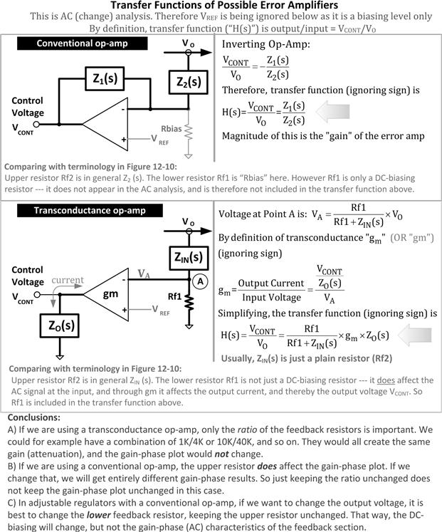
Figure 12.12: Possible feedback stages and some important conclusions in their application.
The analysis is as follows:
• The error amplifier can be a simple voltage-to-voltage amplification device, that is, the traditional “op-amp” (operational amplifier). This type of op-amp requires local feedback (between its output and inputs) to make it stable. Under steady DC conditions, both the input terminals are virtually at the same voltage level. This determines the output voltage setting. But, as discussed previously, though both resistors of the voltage divider affect the DC level of the converter’s output, from the AC point of view, only the upper resistor enters the picture. So the lower resistor is considered just a DC biasing resistor, and therefore we usually ignore it in control loop (AC) analysis.
• The error amplifier can also be a voltage-to-current amplification device, that is, the “gm op-amp” (operational transconductance amplifier, or “OTA”). This is an open-loop amplifier stage with no local feedback — the loop is, in effect, completed externally. The end result still is that the voltage at its input terminals returns to the same voltage (just like a regular op-amp). If there is any difference in voltage between its input pins “ΔV,” it converts that into a current ΔI flowing out of its output pin (determined by its transconductance gm=ΔI/ΔV). Thereafter, since there is an impedance ZO connected from the output of this op-amp to ground, the voltage at the output pin of this error amplifier (i.e., the voltage across ZO — also called the control voltage) changes by an amount equal to ΔI×ZO. For the gm op-amp, both Rf2 and Rf1 enter into the AC analysis, because they together determine the error voltage at the pins, and therefore the current at the output of the op-amp. Note that the divider can in this case be treated as a simple (step-down) gain block of Rf1/(Rf1+Rf2) (using the terminology of Figure 12.10), cascaded with the gm op-amp stage that follows.
Note: We may have noticed that we always use the inverting terminal of the error amplifier for applying the feedback voltage. The intuitive reason for that is that an inverting op-amp has a DC gain of Rf/Rin, where Rf is the feedback resistor (from the output of the op-amp to its negative input terminal) and Rin is the resistor between its inverting terminal and the input-voltage source. So, the output of an inverting op-amp can be made smaller than its input, if so desired (i.e., gain<1). Whereas, a non-inverting op-amp has a DC gain of 1+(Rf/Rin), where Rin in this case is the resistor between its inverting terminal and ground. So, its output will always be greater than its input (gain>1). The resulting restriction has been known to cause some strange and embarrassing situations in the field, especially under abnormal conditions. Therefore, we will almost never see the feedback pin of an IC as being the noninverting input of the error amp.
Lastly, note that by just using an inverting error amplifier, we have, in effect, also applied a −180° phase shift “right off the bat”! We will see in the following section that this increases the possibility of oscillations by itself.
Closing the Loop
We are now in a position to start tying up all the loose ends. For each of the three topologies, we now know both the forward (plant) transfer function G(s) (control-to-output) and the general form of the feedback transfer function H(s). Going back to the basic equation for the closed loop transfer function
![]()
we see that it will “explode” if
![]()
But G(s)H(s) is simply the transfer function for a signal going through the G(s) block, and then through the H(s) block, that is, the open-loop transfer function. We know that the gain is the magnitude of the transfer function (using s=jω), and its phase angle is its argument. Let us calculate what these are for the transfer function −1 above.
![]()
![]()
Note: When doing the tan−1 operation, we may need to visualize where the number is actually located in the complex plane. For example, in this case, tan of 0° and tan of 180° both are zero, and we wouldn’t have known which of these angles is the right answer — unless we actually visualized the number in the complex plane. In our case, since the number was minus 1, we correctly placed it at 180° instead of 0°.
So, we see that the system is unstable if a disturbance (of certain frequency) goes through the plant and feedback blocks, and returns with 180° phase shift and with exactly the same magnitude.
There are two things surprising us here:
(a) We intuitively imagine that a signal reinforces itself only if it returns with the same phase, that is, 360°. So, why are we getting reinforcement with just 180° above? That is because the summing block that follows has one negative and one positive input (it represents a negative feedback system). But that also implies that another 180° shift occurs right here, that is, after the signal leaves the block designated “H(s)” in Figure 12.9 for example. So if the feedback block creates a phase shift of 180°, in effect, we get a total shift of 360°. That explains the positive reinforcement. As we mentioned earlier, the negative feedback functionality (180° shift right off the bat) is automatically included by applying the feedback voltage to the inverting pin of the error amplifier as is conventionally done.
(b) Why do we get positive reinforcement if, not only the phase shift is 180° (a total of 360°), but the returning signal is also of exactly the same magnitude as the cause? This is truly hard to visualize. It may become clearer if we try to draw vector diagrams in the complex plane. We will then see that only if the two above-mentioned conditions are satisfied, can a stable vector diagram result (i.e., we get a sustained oscillation). Otherwise we don’t.
In a typical gain versus frequency plot, we will see that a gain of 1 usually occurs at only one specific frequency, and this is called the “crossover frequency” (see Figure 12.5). Beyond this point the gain becomes less than 1 (i.e., falls below the 0-dB axis).
The stability criterion above is therefore equivalent to saying that the phase shift of the open-loop transfer function should not be equal to 180° (or −180°) at the crossover frequency.
But we also need to ensure a certain margin of safety. This can be expressed in terms of the degrees of phase angle short of 180°, at the crossover frequency. This safety margin is called the “phase margin.” But we could also talk about the safety margin in terms of the amount of gain below 0-dB level at the point where we get 180° phase shift. These are shown in Figure 12.13.
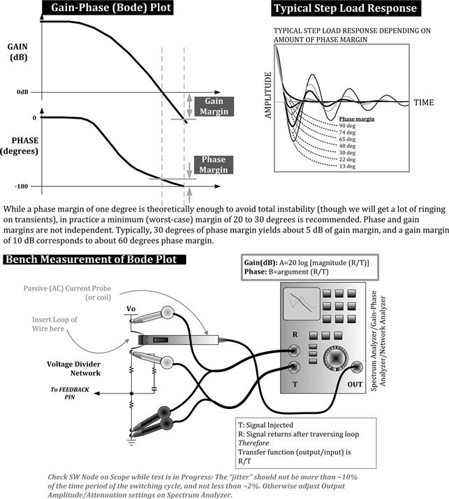
Figure 12.13: Stability margins, measurement and responses.
How much phase margin is enough? In theory, even an overall phase shift of −179° (i.e., a phase margin of 1°) would not produce full instability — though there would certainly be a lot of ringing at every transient, and it would at best be very, very, marginally stable. Component tolerances, temperature variations, and even small changes in the application conditions can change the loop characteristics significantly, ushering in full-blown instability.
It is generally recommended that the phase lag introduced by the successive G and H blocks be about 45° short of −180°, that is, an overall phase lag of −135°. That gives us a phase margin of 45°. But this target phase margin is stated for nominal conditions. In the worst case, we expect a minimum phase margin of around 30°. On the other hand, a phase margin of say 90° may certainly be considered “stable” because we will see no ringing as indicated in Figure 12.13, but it is usually not desirable either. Under transients, the correction may be very sluggish, and so the initial output overshoot/undershoot may be rather severe as discussed previously. A phase margin of 45° would generally be seen to cause just one or two cycles of ringing, and the overshoot/undershoot would also be minimal. However, note that besides phase margin, the crossover frequency also affects the actual step response. The “Q” of any second-order pole located near the crossover point can affect the phase margin significantly and thereby cause ringing. So generally, it is said that we should also ensure that Q of the LC is between 0.5 and 0.707.
Note: Under very large line or load steps, we will actually no longer be operating in the domain of the “small-signal” analysis, which we have been performing so far. In that case, the initial overshoot/undershoot at the output is almost completely determined simply by how large a bulk capacitance we have placed at the output. That capacitance is needed to “hold” the output steady, till the control loop can enter the picture and help stabilize the output. This can determine the size of the output capacitor. See the detailed solved example in Chapter 19.
Criteria and Strategy for Ensuring Loop Stability
We should remember that phase angle can start changing gradually — starting at a frequency even 10 times lower than where the pole or zero may actually reside. We have also seen that a second-order double-pole (−2 slope with two reactive components) can cause a very sudden phase shift of about 180° at the resonant frequency if the Q is very high. Therefore, in practice, it is almost impossible to estimate the phase at a certain frequency, with certainty — nor therefore the phase margin — unless a certain strategy is followed.
One of the most popular (and simple) approaches to ensuring loop stability is as follows:
• Ensure that the open-loop gain crosses the 0-dB axis with a −1 slope.
• The integrator already provides this −1 slope.
• The LC post-filter poses the biggest problem, since after its LC break frequency, the second-order LC pole asks the open-loop gain to fall by an additional −2 slope (taking its slope to −3). The LC pole therefore needs to be canceled out — that is best done by introducing two single-order zeros exactly at the location of the LC pole.
• We also want to maximize the bandwidth to achieve quick response to extremely sudden load or line transients. By sampling theory, we know that we certainly need to set the crossover frequency to less than half the switching frequency.
• We also need to ensure that the crossover frequency is kept well below any troublesome poles or zeros — like the RHP zero for example. Keep in mind that the RHP zero occurs in CCM for the Boost and the Buck-Boost topologies, irrespective of whether we are using voltage-mode or current-mode control, and at any duty cycle. We should also try to avoid the “subharmonic instability pole” which occurs at half the switching frequency — in CCM in the Buck, Boost, and Buck-Boost topologies, when using current-mode control with D>50%. This is discussed later.
So, in practice, most designers set the crossover frequency at about one-sixth the switching frequency (for voltage-mode control).
In Figure 12.13, we have also presented the most common method of generating a Bode plot and measuring stability margins on the bench. Obviously, more exotic techniques are required for injecting the disturbance if the voltage divider location shown in Figure 12.13 is not available for us to insert a current loop or a small resistor.
Plotting the Open-Loop Gain for the Three Topologies
Now we want to finally start plotting the gain and phase of the open-loop transfer function T(s)=G(s)H(s) since we know that that is the function critical to ensuring stability. As background, we have understood math in the log-plane and also the interaction of poles and zeros, whether they are on the same transfer function plot, or on more than one cascaded transfer function plots (which are being combined to provide the open-loop gain). We have also derived the plant transfer functions of all topologies and understood the basic strategy for ensuring stability. We also know that the integrator is a fundamental building block in the feedback path, without which we will have very inadequate DC regulation. Now we can put it all together.
On the left side of Figure 12.14, we have only a pure integrator in the feedback path of a Buck. We realize that the open-loop gain crosses over on the 0-dB axis with −3 slope, which is not as per our strategy. Therefore, we actually ignore the results here and introduce two zeros in the feedback loop, exactly at the location of the LC pole. This is as per our basic strategy. We see that now, indeed, the open-loop gain crosses over with a −1 slope. This is acceptable. In the same figure, we have provided the overall DC gain of the power stage and the crossover frequency (bandwidth) of the feedback loop. All this will lead to adequate phase margin. We have completed the Buck analysis. Later we will show what specific circuitry is required to place the two zeroes exactly where we have declared them to be.
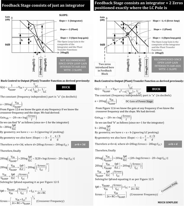
Figure 12.14: Stabilizing a Buck converter and calculating its crossover frequency and DC gain of power stage (recommended method is on the right side).
In Figure 12.15, we have carried out the same calculation steps for the Boost and the Buck-Boost. Here we are assuming we have crossed over at a low-enough frequency so that the RHP zero is well outside the bandwidth of the loop, and therefore cannot affect the plots as shown.
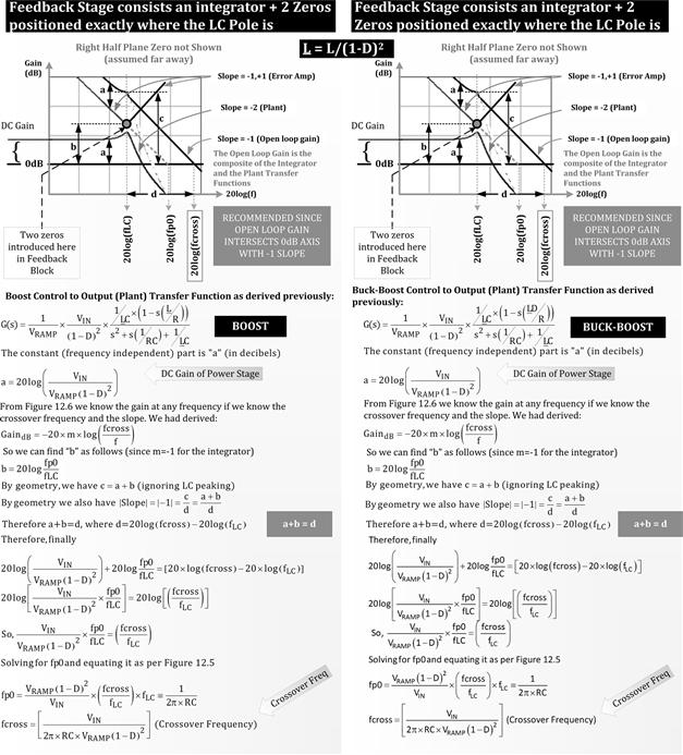
Figure 12.15: Stabilizing Boost and Buck-Boost converters and calculating their crossover frequency and DC gain of power stage.
We realize that after canceling out the LC pole, we are left with a simple −1 plot for the open-loop transfer function. This is just the transfer function of the integrator, shifted upward by the amount “a” as indicated in Figures 12.14 and 12.15. Note that “a” is the DC gain of the power stage. We already have the equations for “a” embedded in the two figures. We can thus calculate the effect of this vertical shift on the crossover frequency, as per the math presented in the lower half of Figure 12.6, namely
![]()
Here f1 is fp0 and f2 is fcross. We therefore get
![]()
where for a Buck, for example (Figure 12.14), we have
![]()
We therefore get
![]()
(since 10log(x)=x)
So,
![]()
Similarly, for the Boost and the Buck-Boost, we get
![]()
This tells us where to set fp0 for the integrator section, when targeting a certain crossover frequency fcross for the open-loop gain. We will give a numerical example later.
Our overview of compensation analysis seems complete. However, there is one last complication still remaining. Besides two zeros, we may need at least one pole from our compensation network (besides the pole-at-zero of the integrator section). This is for canceling out the “ESR-zero” coming from the output capacitor. We have been ignoring this particular zero so far, but it is time to take a look at it now.
The ESR-Zero
We ignored the ESR of the output capacitor in Figures 12.14 and 12.15, and also in the derivation of all the transfer functions carried out earlier. For example, we had earlier provided the following control-to-output transfer function for a Buck:
![]()
where ω0=1/√(LC). The ESR-zero adds an additional term to the numerator. A full analysis shows that the control-to-output transfer function now becomes
![]()
where ωESR=1/((ESR)×C) is the frequency (in radians per second) at which the ESR-zero is located. Judging by the sign in front of the s-term in the numerator, this is a “well-behaved” (left-half-plane) zero. But it does try to cause an increase in the slope of the open-loop transfer function by +1 and may thus even prevent crossover from occurring properly, besides affecting the phase significantly too. It is also based on a parasitic, which is not a guaranteed parameter. So, it is usually considered a nuisance. Though in some simpler compensation network types, the ESR-zero may even be counted upon to provide one of the two zeros required to cancel out the LC double-pole, as discussed previously. It may not be at the “right place,” but it can still work. In general, however, the ESR-zero is considered avoidable or worth getting rid of (by a pole).
In the best case, the ESR will be very small, and so its zero will be far away (at a very high frequency). We can then simply ignore it. That situation arises when we use modern ceramic output caps for example. Otherwise, the preferred strategy is to place a pole at exactly the location of the ESR-zero, thereby canceling it out.
High-Frequency Pole
We have seen that a full-blown compensation network needs to provide
(a) a pole-at-zero (integrator function)
(b) two zeros at the location of the LC double-pole
Where did the last one come from? In general, for making the control loop less sensitive to high-frequency switching noise, designers often put another pole roughly at about 10 times the crossover frequency (some recommend half the switching frequency). So, now the gain will cross the 0-dB axis with a slope of −1 as per our strategy, but at higher frequencies it will suddenly drop off more rapidly, close to a −2 slope. That will improve the Gain margin shown in Figure 12.13.
Why do some designers pick 10 times the crossover frequency above? Because the phase introduced by this new high-frequency pole will actually start making itself felt at one-tenth the frequency of the pole, and we didn’t want to adversely impact the phase angle in the vicinity of the crossover frequency (i.e., the phase margin). But we realize that the resulting open-loop gain plot is just a vertically shifted −1 plot coming from the integrator section. We also know that a single-pole provides 90° phase shift. So, we could be left with a phase margin of 180−90=90°, which may be considered sloppy. Therefore, some designers try to move this high-frequency pole to a much lower frequency, just a little higher than the crossover frequency, to deliberately reduce the phase margin in a calculated manner — closer to the target value of 45°.
Designing a Type 3 Op-Amp Compensation Network
Three types of error amplifier compensation schemes are used most often — called the Types 1–3 in order of increasing complexity and flexibility. The former two are just a subset of the latter, so we will now just do a Type 3 compensation to demonstrate the full scope (though usually, Type 2 compensation should suffice).
The transfer function of a Type 3 error amplifier as shown in Figure 12.16 can be worked out easily in the manner we did before. It is given in detail in the figure, but it can also be written more generically as follows:
![]()
where ωp0=2π(fcross), ωz1=2π(fz1), and so on. Note that we are ignoring the minus sign in front of this transfer function, as we are separating out the 180° phase shift inherent in negative feedback systems.
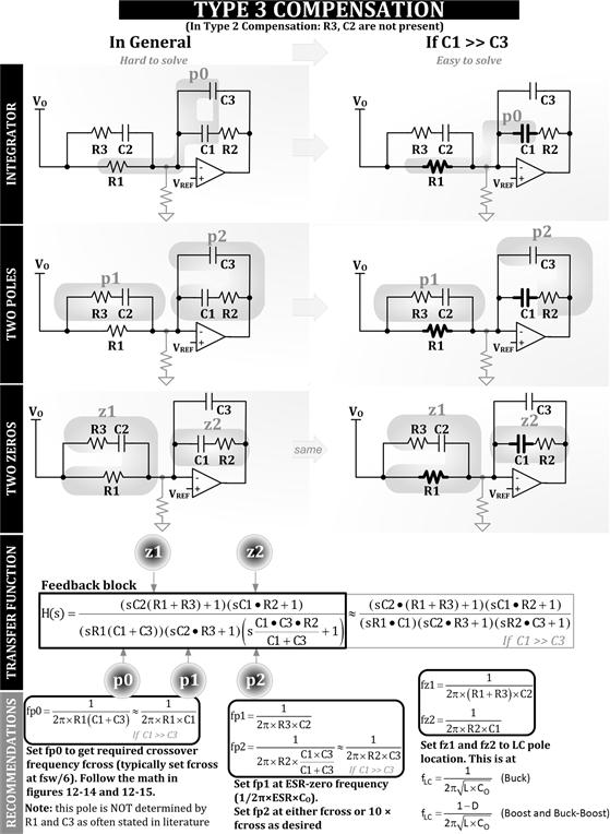
Figure 12.16: Conventional type 3 compensation using conventional voltage Op-Amp.
There are two poles “p1” and “p2” (besides the pole-at-zero “p0”) and two zeros “z1” and “z2” provided by this compensation. Note that several of the components involved play a dual role in determining the poles and zeros. So, the calculation can become fairly cumbersome and iterative. But a valid simplifying assumption that can be made is that C1 is much greater than C3. So the locations of the poles and zeros are finally
![]()
![]()
![]()
![]()
![]()
Note that for convenience, the reference designators of the components have changed somewhat in this section. In particular, what we are now calling “R1” was “Rf2” when we previously discussed the voltage divider. Similarly, the gray unnamed resistor in Figure 12.16 was previously called “Rf1.”
We can also solve for the values of the components (with the approximation C1 » C3). We get
![]()
![]()
![]()
![]()
Let us take up a practical example to show how to proceed in designing a feedback loop with this type of compensation.
Example:
Using a 300-kHz synchronous Buck controller we wish to step-down from 15 V to 1 V. The load resistor is 0.2 Ω (5 A). The PWM ramp is 2.14 V as per the datasheet of the part. The selected inductor is 5 μH, and the output capacitor is 330 μF, with an ESR of 48 mΩ.
We know that the plant gain at DC for a Buck is VIN/VRAMP=7.009. Therefore, (20×log) of this gives us 16.9 dB. The LC double-pole is at
![]()
(note that for a Boost and Buck-Boost, the location of the LC pole is given in Figure 12.16, based on the canonical model). We want to set the crossover frequency of the open-loop gain at one-sixth the switching frequency, that is, at 50 kHz. Therefore, we can solve for the integrator’s fp0 and thereby its “RC,” by using the equation presented earlier.
![]()
So, in our case,
![]()
If we have selected R1 as say 2 kΩ, C1 is then
![]()
The crossover frequency of the integrator section of the op-amp is
![]()
The ESR-zero is at
![]()
The required placement of zeros and poles is
![]()
![]()
![]()
The components required to make this happen are
![]()
![]()
![]()
![]()
We already know C1 is 11.16 nF and R1 was selected to be 2 kΩ. The results of this example are plotted in Figure 12.17.
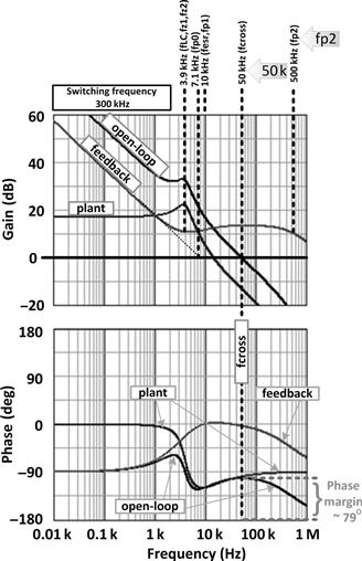
Figure 12.17: Plotting the results for the Type 3 compensation example (standard setting).
Note that for a Boost or Buck-Boost, the only changes required in the above analysis are
![]()
![]()
However, in the case of the Boost and Buck-Boost, we must also always ensure that the selected crossover frequency is at least an order of magnitude below the RHP zero (whose location was provided previously).
Optimizing the Feedback Loop
In Figure 12.17, we have plotted the results of the previous example, and we can see that though the crossover frequency is high enough, the phase margin is rather too generous. A very high phase margin may be considered “very stable” with no ringing, but the overshoot/undershoot can improve further if the phase margin is closer to 45°.
We should have realized by now that intuitively, poles are generally responsible for making matters “worse” — since they always introduce a phase lag, leading us closer to the danger level of −180°. On the other hand, zeros boost the phase angle (phase lead), and thereby help to cause the phase margin to increase. Therefore, to decrease the existing phase margin of 79° to say 45°, we need another pole. The new criterion to set the high-frequency pole fp2 becomes
![]()
We are calling this the “optimized setting” here.
We can guess that the phase shift introduced by a single-pole at its resonant frequency is 45°, so the new phase margin should be around 79°−45°=34°. We plot the gain-phase plots with this new high-frequency pole criterion (and with freshly calculated compensation component values), and we get the curve shown in Figure 12.18.
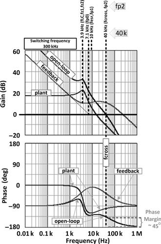
Figure 12.18: Plotting the results for the Type 3 compensation example (optimized setting).
In Figure 12.18, we see that the phase margin is now almost exactly 45°. The reason it is a little more than our initial estimate of 34° (though we desired 45°) is that the crossover frequency has decreased slightly to 40 kHz. It can be shown that by trying to place the high-frequency pole exactly at the crossover frequency, the crossover frequency itself shifts downward by almost exactly 20%. So the corollary to that is — if we are starting a compensation network design in which we are going to use the high-frequency pole in this “optimized” manner, we should initially target a crossover frequency about 20% higher than we desire.
Note: We can understand the lowering of the crossover frequency in the “optimized setting” case as follows. In terms of the asymptotic approximation, the open-loop gain crosses the 0-dB axis with a slope of −1, but then immediately thereafter falls off at a slope of −2. But since the high-frequency pole fp2 is placed very close to the crossover frequency, the gain in reality falls by 3 dB at this break-point (as compared to the asymptotic approximation). So, the actual crossover occurs a little earlier. The reason the phase is affected by almost 45° at the crossover frequency is that phase starts changing a decade below where the pole really is.
Engineers use various other “tricks” to improve the loop response further. For example, they may “spread” the two zeros symmetrically around the LC double-pole (rather than coinciding exactly with it). One reason to put a zero (or two) slightly before the LC pole location is that the LC pole can produce a very dramatic 180° phase shift, and this can lead to “conditional stability.” So, the spreading of zeros around absorbs some of the phase shift abruptness.
Conditional stability is said to occur if the phase gets rather too close to the −180° danger level at some frequency. Though oscillations do not normally occur at this point, simply because the gain is high (crossover is not taking place at this location), under large-signal disturbances, the gain of the converter can suddenly fall momentarily toward 0 dB, thus increasing the chance of instability. For example, if there is a very large change in line and load, the error amplifier output may “rail,” that is, reach a value close to its internal supply rails. Its output transistors may then saturate, taking a comparatively long time to recover and respond. So, the gain would have effectively decreased suddenly, and it could end up crossing the 0-dB axis at the same location where the phase angle happens to be −180° — and that would meet the criterion for full-blown instability.
Input Ripple Rejection
The line-to-output transfer function of the Buck was shown to be
![]()
The plant transfer function was
![]()
We see that the line-to-output transfer function for the Buck is the same as its control-to-output transfer function, except that the VIN/VRAMP factor is replaced by D.
So, for example, if VRAMP=2.14 V and D=0.067 (as for 1 V output from a 15 V input), then the control-to-output (plant) gain at low frequencies is
![]()
and the line-to-output transfer gain at low frequencies must be
![]()
The latter represents attenuation, since the response at the output is less than the disturbance injected into the input. But both the above-mentioned DC gains are without feedback considered. Alternatively, we have implicitly assumed that the error amplifier is set to a gain of 1, and there are no capacitors present anywhere in the compensation network. However, when feedback is present (“loop closed”), it can be shown by control loop theory that the line-to-output transfer function changes to
![]()
where T=GH. Since T (the open-loop transfer function) at low frequencies is very large, we can write T+1≈T. Further, since 20×log(1/T)=−20×log(T), we conclude — at low frequencies, the additional attenuation provided, when the loop is closed, is equal to the open-loop gain. For example, if the open-loop gain at 1 kHz is 20 dB, it attenuates a 1-kHz line disturbance by an additional 20 dB — over and above the attenuation already present without feedback considered. That is one reason why we are always so interested in increasing the DC gain in general (the purpose of the integrator).
For example, suppose we are interested in attenuating the 100-Hz (low-frequency) ripple component of the input voltage in an off-line power supply down to a very small value. If our crossover frequency is 500 kHz, then using the simple relationship derived in Figure 12.6, we can find the open-loop gain at 100 Hz. Here we are assuming we have carried out the recommended pole-zero cancelation compensation strategy, which leaves us with an open-loop gain plot that has a pole-at-zero type response (−1 slope). So, the gain at 100 Hz is
![]()
Expressed in dB, this is
![]()
So, the additional attenuation is 54 dB here. Suppose the duty cycle of the converter is 30%. Assuming it is a Forward converter with Buck-like characteristics, and its duty cycle is 30%, the line-to-output transfer function will provide a DC attenuation of |20×log(D)|=10.5 dB. So, by introducing feedback, the total low-frequency attenuation has increased to 54+10.5=64.5 dB. This is equivalent to a factor of 1064.5/20=1,680. So, if for example, the low-frequency ripple component at the input terminals was ±15 V, then the output will see only±15/1680=±9 mV of line ripple.
Load Transients
Suppose we suddenly increase the load current of a converter from 4 A to 5 A. This is a “step load” and is essentially a nonrepetitive stimulus. But by writing all the transfer functions in terms of s rather than just as a function of jω, we have created the framework for analyzing the response to such disturbances too. We will need to map the stimulus into the s-plane with the help of the Laplace transform, multiply it by the appropriate transfer function, and that will give us the response in the s-plane. We then apply the inverse Laplace transform and get the response with respect to time. This was the procedure symbolically indicated in Figure 12.2, and that is what we need to follow here too. However, we will not perform the detailed analysis for arbitrary load transients here, but simply provide the key equations required to do so.
The “output impedance” of a converter is the change in its output voltage due to a (small) change in the load current. With feedback not considered, it is simply the parallel combination of R, L, and C. So,
![]()
where R is the load resistance, and L is the actual inductance L for a Buck, but it is L/(1−D)2 for a Boost and a Buck-Boost.
With feedback considered, the output impedance now decreases as follows:
![]()
Even without a detailed analysis (using Laplace transform), this should tell us by how much the output voltage will eventually shift (settle down to), if we change the load current.
Type 1 and Type 2 Compensations
In Figure 12.19, we have also shown Type 1 and Type 2 compensation schemes (though with no particular strategy in placing the poles and zeros). These are less powerful schemes than Type 3. So, Type 3 gives us one pole-at-zero AND two poles AND two zeros, and Type 2 gives us one pole-at-zero AND one pole AND one zero. However, Type 1 gives us ONLY a pole-at-zero (simple integrator).
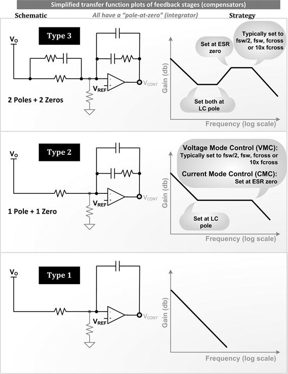
Figure 12.19: Types 1–3 compensation schemes (poles and zeros arbitrarily placed and displayed).
We know that we always need a pole-at-zero in the compensation for achieving high DC gain, good DC regulation, and low-frequency line rejection. So, the −1 slope coming from the pole-at-zero adds to the −2 slope from the double-pole of the LC-filter, and this gives us a −3 slope — that is, if we don’t put in any more zeros and poles (as shown on the left side of Figure 12.14). But we want to intersect the 0-dB axis with a −1 overall slope. So, that means we definitely need two (single-order) zeros to force the slope to become −1.
Therefore, Type 2 compensation can also be made to work because though it provides only one zero, we can use the zero from the ESR of the output capacitor (despite its relative unpredictability). We remember, in Type 3, we canceled the ESR-zero out completely, citing its relative unpredictability. But now we can consider using it to our advantage, if that is, indeed, possible: for the Type 2 scheme to work, the ESR-zero must be located at a lower frequency than the intended crossover frequency.
Type 2 compensation is well suited for current-mode control, as explained later. Type 1 compensation provides only a pole-at-zero and, in fact, can only work with current-mode control, provided the ESR-zero is also below crossover.
Transconductance Op-Amp Compensation
The final stages of the analysis of voltage-mode controlled converters are reserved for the transconductance op-amp. In Figure 12.12, we had presented its transfer function generically. Now let us consider the details of implementing a compensation scheme.
We can visualize this feedback stage as a product of three cascaded transfer functions, H1, H2, and H3 as shown in Figure 12.19. When we plot the separate terms out as in the lower part of the figure, we see that this looks like Type 3 compensation — but in reality it is not! Because, though it provides two zeros and two poles (besides the inevitable pole-at-zero), we see a big difference — in the behavior of H1 (the input side). The problem is that if we fix pole fp2 at some frequency, the location of the zero fz2 is automatically defined. They are not independent. There is therefore no great flexibility in using this zero and pole pair. For example, if we try to fix both zeros of the overall compensation network at the LC double-pole frequency, the pole fp2 will be literally dragged along with fz2, and so the overall open-loop gain would finally fall at −2 slope again, not at −1 as desired. Therefore, the zero of H1 (fz2) can only be used if the associated pole fp2 is at or beyond the crossover frequency. A possible strategy for placing the poles and zeros is indicated in Figure 12.19. But more often, Cff is just omitted, which leaves us with a simple voltage divider composed of resistors. In that case, we get H1(s)=Rf1/(Rf1+Rf2) as expected.
It actually requires a great deal of mathematical manipulation to solve the simultaneous equations and to come up with component values for a desired crossover frequency. Therefore, the derivation is not presented here, and the steps are in accordance with the basic math-in-the-log-plane tools presented in Figure 12.6. The final equations are presented below through a numerical example, similar to what we did for Type 3 compensation with regular op-amps.
Example:
Using a 300-kHz synchronous Buck controller we wish to step-down from 25 V to 5 V. The load resistor is 0.2 Ω (25 A). The ramp is 2.14 V from the datasheet of the part. The selected inductor is 5 μH, and the output capacitor is 330 μF, with an ESR of 48 mΩ. The transconductance of the error amplifier is gm=0.3 (units for transconductance are “mhos,” i.e., ohms spelled backward). The reference voltage is 1 V.
The LC double-pole occurs at
![]()
We choose our target crossover frequency “fcross” as 50 kHz. Suppose we pick Rf2=4 kΩ and Rf1=1 kΩ based on the voltage divider equation, the output voltage (5 V) and the reference voltage of 1 V. Then
![]()
The crossover of the overall feedback gain (H) occurs at a frequency “fp0” as indicated in Figure 12.20, where
![]()
So,
![]()
![]()
![]()
Figure 12.20: “Full-blown” transconductance operational amplifier compensation (voltage-mode control).
We have presented the computed gain-phase plots in Figure 12.21. The computed crossover frequency is 40 kHz (a little less than our target of 50 kHz, so we may want to target 20% higher than we want, to start with).
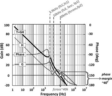
Figure 12.21: Plotting the results of the “full-blown” transconductance Op-Amp-based compensation example (voltage-mode control).
Note that the location of fz2 was not fixed by us, but automatically positioned itself once we set fp2 to 50 kHz (the expected fcross, though that turned out to be ~40 kHz). The location of fz2 in Figure 12.21 can be calculated based on the equation in Figure 12.20 as follows:
![]()
Note that the ESR-zero location is
![]()
The above two equations are coincidentally the same in our example. But that also means, since we positioned fp1 (the other remaining pole) at the ESR-zero location, in this example, we have an overlap of fz2, fesr, and fp1 as shown in Figure 12.21. In fact, fp0 at 10.9 kHz is also very close (not shown).
From Figure 12.21, we see that we have an adequate 40° of phase margin.
Note: We started above example with a rather small output capacitance and large ESR than typically used for this particular application and power level. That is why C1 is also not much larger than C2. The intention was to shift the ESR-zero to less than the crossover frequency, to demonstrate the principles and also to be able to plot the gain curves easily as in Figure 12.21. However, the equations and procedure presented are valid for any output capacitance and ESR.
Simpler Transconductance Op-Amp Compensation
As mentioned, there is a practical difficulty involved in using the “full-blown” transconductance op-amp compensation scheme discussed above — because the pole and zero arising from H1 are not independent. They will even tend to coincide if say Rf2 is much smaller than Rf1 (i.e., if the desired output voltage is almost identical to the reference voltage).
So, now we try a simpler transconductance stage shown in Figure 12.22. The equations for this, based on a new compensation strategy, are presented in the following (new) example. Note for visual clarity in plotting that both the L and the C values used here are different from those of previous examples.
Example:
Using a 300-kHz synchronous Buck controller, we wish to step-down from 25 V to 5 V. The load resistor is 0.2 Ω (25 A). The ramp is 2.14 V from the datasheet of the part. The selected inductor is 50 μH, and the output capacitor is 150 μF, with an ESR of 48 mΩ. The transconductance of the error amplifier is gm=0.3 (mhos), and the reference voltage is 1 V.
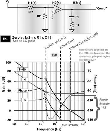
Figure 12.22: Plotting the results for the simpler transconductance Op-Amp-based compensation example (voltage-mode control).
As before, Rf1/(Rf1+Rf2)=VREF/VO=1 V/5 V=0.2.
The LC double-pole occurs at
![]()
We choose our target crossover frequency “fcross” as 100 kHz.
The crossover of the feedback gain plot (H) occurs at a frequency:
![]()
To achieve this fp0, we need
![]()
![]()
Note that the ESR-zero location is
![]()
We have presented the computed gain-phase plots in Figure 12.22. We see we have a generous 78° of phase margin and a crossover frequency of 100 kHz.
Based on the logic presented for the Type 3 compensation scheme (non-optimized case, see later), the phase margin in this case was also expected to be around 90°. And once again, one way to reduce the phase margin closer to the optimum of 45°, is to reintroduce C2 in Figure 12.20, which brings back fp1. We then set fp1 exactly at fcross as previously explained. We then get
![]()
By reintroducing C2, the computed crossover again occurs slightly earlier (by about 20%) — at around 80 kHz, instead of 100 kHz, so we may want to target 20% more than we want. The phase margin is now 36° (closer to the optimal).
Also note that for this simpler compensation scheme to work, the ESR-zero must lie between the LC pole frequency and the selected crossover frequency. Otherwise this will not work with voltage-mode control.
Note that for a Boost or Buck-Boost, the only changes required in the above analysis are
![]()
![]()
However, we must also always ensure (for these two topologies) that the selected crossover frequency is at least an order of magnitude below the RHP zero.
Compensating with Current-Mode Control
The plant transfer functions presented earlier were only for voltage-mode control. In current-mode control, the ramp to the PWM (for determining duty cycle) is derived from the inductor current. It can be shown that if we do that, the inductor effectively goes “out of the picture” in the sense that there is no double LC pole anymore. So, the compensation is supposedly simpler, and the loop can be made much faster. However, the actual mathematical modeling of current-mode control has proven extremely challenging — mainly because there are now two feedback loops in action — the normal voltage feedback loop (slower) and a current feedback loop (cycle-by-cycle basis; much faster). Various researchers have come up with different approaches, but they don’t seem to agree completely with each other yet.
Having said that, everyone does seem to agree that current-mode control alters the poles of the system compared to voltage-mode control, but the zeros of voltage-mode control remain unchanged. So, the Boost and the Buck-Boost still have the same (low-frequency) RHP zero, as we discussed earlier (i.e., that applies to voltage-mode and current-mode controls when we are operating in CCM). Therefore, care is still needed to ensure that the RHP zero is at a much higher frequency than the chosen crossover frequency.
As mentioned, in current-mode control, the ramp to the PWM comparator is derived from the inductor current. Actually, the most common way of producing the ramp is to simply sense the forward-drop across the MOSFET (or of course by using an external sense resistor in series with it) (see Figure 12.23 (top half)). This small sensed voltage is then amplified by a “current sense amplifier” to get a voltage ramp, which is then applied to the PWM comparator. On the other pin of the PWM comparator, we have the usual output of the error amplifier (control voltage).
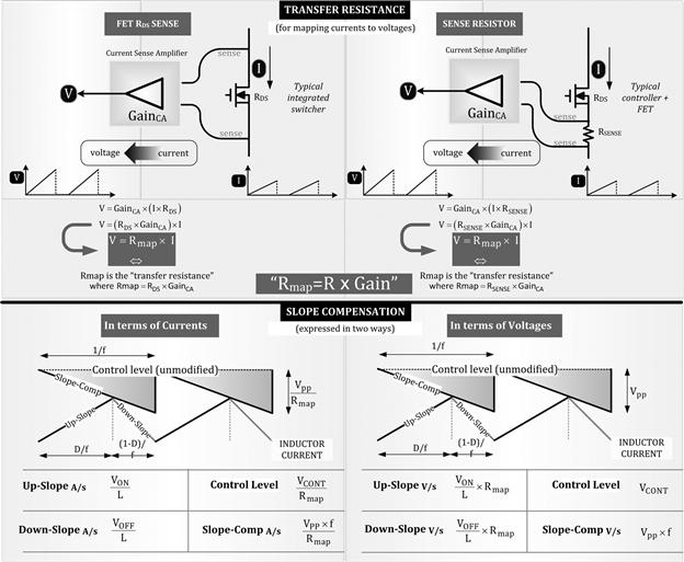
Figure 12.23: How the “transfer resistance” maps the current in the switch, into a voltage sawtooth at the comparator input, and how slope compensation can be expressed in terms of either voltages or currents.
The inductor/switch current ramp is now obviously proportional to the voltage ramp received at the PWM comparator input. So, voltages and currents can be converted (mapped) between each other through the use of the “transfer resistance” V/I, as defined in Figure 12.23. We can look at the overall effect either in terms of ALL currents, or in terms of ALL voltages, as shown in the lower half of Figure 12.23.
Slope compensation, as discussed in more detail later, can also be expressed either as a certain applied A/s (or A/μs), or as an applied V/s. These are all equivalent ways of talking about the same thing, since voltages and currents are proportional to each other — through the transfer resistance. For example, if we know that a peak current of 1 A on the sense resistor appears as a peak voltage of 1.5 V at the PWM comparator input, the transfer resistance is simply V/I=1.5/1=1.5 Ω. Yes, we do need to have inside information on the part, in particular the peak-to-peak voltage swing of its error amplifier output (which in turn determines the maximum swing of the mapped inductor current).
Note that since the ramp itself gets terminated at the exact moment when it reaches the control voltage level (because it is a comparator), in effect, we end up regulating the peak of the inductor current ramp. So, what we are discussing here is really just “peak current-mode control.” Many experienced designers prefer “average current-mode control.”
One of the subtleties of current-mode control is that (for all the topologies) we need to add a small artificial ramp to stabilize it under certain conditions. This is called slope compensation. Its purpose is to prevent an odd artifact of current-mode control called “subharmonic instability.” Subharmonic instability usually shows up as alternate wide and narrow switching pulses (a pattern that repeats itself at the rate of half the switching frequency). In steady-state operation, we may not realize it is present. There may just be a small output ripple, one that can be further suppressed by large-enough output caps. It will, however, manifest itself as a badly degraded transient response. Its Bode plot will also very likely not even be recognizable as one — there may be no way to even describe a phase margin in that plot. In general, we really need to look at the switching node waveform to rule out subharmonic instability conclusively.
Note: All patterns that repeat themselves at the rate of fsw/2 need not represent subharmonic instability — even noise spikes, for example (self-generated or from synchronized external sources), can cause the same effect, by producing early termination of an ongoing pulse, that forces a longer succeeding pulse, in an effort to meet the required energy demand.
What are the causes of this instability and the solution? In Figure 12.24, we have shown the control voltage (output of the error amplifier), plotted against the mapped inductor current (these are the voltages on the two pins of the PWM comparator). Therefore, whenever the (mapped) inductor current equals the control voltage level, the pulse is terminated as shown. Note that the control voltage is no longer flat as in conventional voltage-mode control, but has a negative sawtooth superimposed on it as seen in Figures 12.23 and 12.24. This is called “slope compensation” or “ramp compensation,” and it represents a possible solution to subharmonic instability. The problem itself is described in Figure 12.24. We see that a small input disturbance Δ1, becomes Δ2 after the given pulse ends, and that becomes the input disturbance going into the next on-time. This will become Δ3 in the next pulse, and so on. The ratio by which the disturbance changes every cycle, using the simple geometry shown in the figure, is
![]()
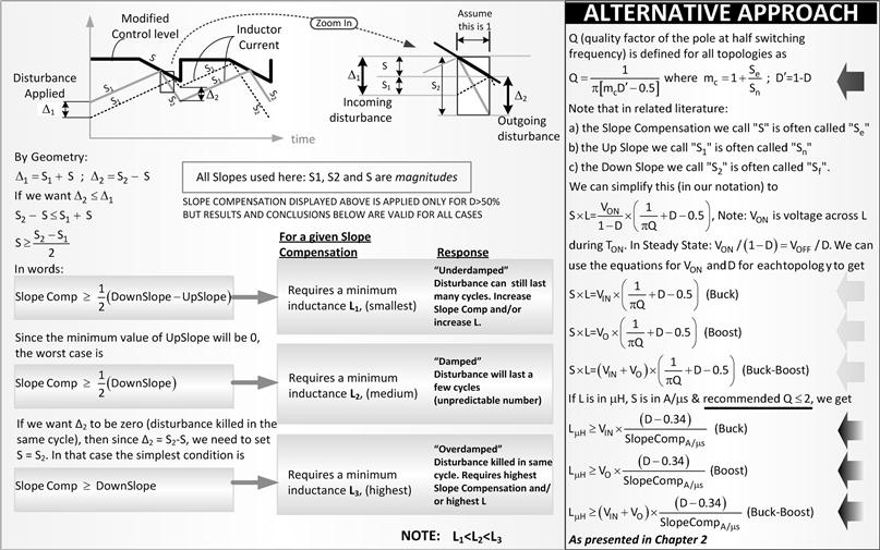
Figure 12.24: Explaining the conditions for avoiding subharmonic instability: traditional approach on the left, modern alternative method on the right (set Q<2).
If we want the disturbance to subside eventually, the condition is
![]()
where S2 is the down-slope of the inductor, S1 the up-slope, and S the applied slope compensation. It should be obvious that all these three slopes must be in the same units. So, we can have them all expressed as A/μs, or all expressed as V/μs. To do that, we just need to know Rmap.
For subharmonic instability to occur, two conditions have to be met simultaneously — the duty cycle should be close to or exceed 50%, and simultaneously, we should be in CCM. Note that the propensity to enter this subharmonic instability state increases as the duty cycle increases (i.e., as the input is lowered). So, we should always try to rule out this instability at VINMIN. We could certainly avoid this problem altogether, by choosing DCM (discontinuous conduction mode). But otherwise, in CCM, slope compensation is the recognized sure-fix. Though it is interesting to note that by applying slope compensation, we are, in effect, blending a little voltage-mode control with a current-mode control. Note that to do this we could do either of the two below:
(a) Take the sensed current ramp generated from the switch/inductor current, convert it to an equivalent sensed voltage (via Rmap), and to that add a small fixed voltage ramp.
Note: In the popular off-line controller IC UC3842, designers often add a small 10–20-pF capacitor between the clock pin (Pin 4) and the current sense pin (Pin 3). This is a simple slope compensation trick, undocumented in the datasheet of the part. The purpose of that was to add a little bit of the fixed clock signal ramp to the sensed current ramp (which would go to the PWM comparator). In effect, we are thus mixing a little voltage-mode control to current-mode control, as we declared was the intuitive purpose of slope compensation. In the UC3844, the duty cycle cannot exceed 50%, since it is meant for Forward converters, not for flybacks. So, this trick was not necessary for that IC.
(b) Since we are talking in terms of relative voltages at the input of a comparator, we could equivalently modify the control voltage itself (the output of error amplifier) as shown in Figures 12.23 and 12.24. The intent is, especially for duty cycles greater than 50% (where subharmonic instability can occur), we progressively decrease the control voltage steadily as the cycle progresses.
Note: Applying slope compensation as shown in Figures 12.23 and 12.24 may limit the peak current and thereby the max power of the converter when the duty cycle exceeds 50%. To avoid that, designers often design in a progressively higher current limit at large duty cycles.
Note: Though for simplicity, we have not shown it explicitly in Figure 12.23, in true current-mode control, we should not lose the “DC” (pedestal) information of the inductor/switch current.
What are the symptoms of impending subharmonic instability? If we take the Bode plot of any current-mode controlled converter (one that has not yet entered this wide-narrow-wide-narrow state), we will discover an unexplained peaking in the gain plot, at exactly half the switching frequency (similar to the peaking in Figure 12.7). This is the “source” of potential subharmonic instability. Note that we never consider setting the crossover frequency higher than half the switching frequency. So, in effect, this subharmonic pole will always occur at a frequency greater than the crossover frequency. However, we realize that the effect of this pole on the phase angle may start at a much lower frequency. Even strictly in terms of gain, this half-switching frequency pole remains dangerous because of the fact that if it peaks too much, it can end up causing the gain plot to intersect the 0-dB axis again. This represents another unintended crossover, and we know that any phase reinforcement at crossover can provoke full instability.
Subharmonic instability is nowadays modeled as a complex pole at half the switching frequency. It has a certain “Q” as described on the right side of Figure 12.24. By actual experiments, it has been shown that a Q of less than 2 typically creates stable conditions. A Q of 1 is preferred by conservative designers, and though that does quell subharmonic instability even more firmly, it does lead to a bigger inductor (producing a non-optimum current ripple ratio r of less than 0.4). Alternatively, we need to apply greater slope compensation. But too much slope compensation is akin to making the system more and more like voltage-mode control, and pretty soon, especially at light loads, the double LC pole of voltage-mode control will reappear, potentially causing instability of its own.
In Figure 12.24, we have also presented the modern method for dealing with subharmonic instability. We have thereby proven the relations presented earlier in Chapter 2 for (minimum) inductance. These equations are
![]()
![]()
![]()
Having taken care of subharmonic instability by a suitable choice of inductance and/or slope compensation, we will no longer include it in the following analysis in which we set the poles and zeros of the compensation network.
The design equations presented for the compensation network below are based on a simpler model from Middlebrook that reduces current-mode control to something similar to voltage-mode control discussed previously. The purpose of that is to make current-mode control amenable to being handled in a familiar fashion too — as a product of several cascaded transfer functions, rather than parallel feedback loops.
The results from the Middlebrook model give a good match with far more elaborate models — provided we have taken precautionary steps. For example, we need to ensure the RHP zero (if present) is designed out (we should check its location is at least a decade away from the target crossover frequency). We should also check that the fsw/2 subharmonic pole is higher than the crossover frequency, and also that the fsw/2 pole is sufficiently damped as discussed above. If so, we can proceed as follows.
Note that in our presentation below, we are even ignoring some other poles from Middlebrook’s original model, on the grounds that they usually fall well outside the crossover frequency, and are therefore of little practical interest.
In our extra-simplified model, we are thus left with only a single-pole in the plant transfer function for all the topologies. This pole comes from the output capacitor and the load resistor (the “output pole”). When we combine it with the inevitable pole-at-zero (from the integrator section of the op-amp), the overall (open-loop) gain will fall with a slope of −2 (after the output pole location). Therefore, we need just one single-zero to cancel part of this slope out, and finally get a −1 slope with which to crossover as desired. Further, this single-zero can either be deliberately introduced using Type 2 compensation (in which case we could use its available pole to cancel out the ESR-zero) — or we could simply rely on the naturally occurring ESR-zero of the output cap. In the latter case, we would need to ensure that the ESR-zero is at a frequency lower than the crossover frequency. Alternatively, that could indirectly force us to move the crossover frequency out to a higher frequency (but without getting too close to the other trouble spots mentioned above).
The design equations and steps for the transconductance op-amp are as follows (see left side of Figure 12.26).
(a) Choose a crossover frequency “fcross.” Although we would like to typically target one-third the switching frequency, we must manually confirm that this frequency is significantly below the location of the RHP zero (the equations for the RHP zero were presented earlier, and they still apply here).
(b) We realize that, once again, while plotting the open-loop gain, the gain of the integrator will shift vertically by the amount GO (DC gain of plant). Therefore, using the simple rule in the lower half of Figure 12.6, we can find the required fcross that will lead to the desired crossover frequency (of the open-loop gain). So,
![]()
where the values of GO=A/B are presented in Figure 12.25.
![]()
where y is the “attenuation ratio” in Figure 12.26.
![]()
where fP is the output pole of the plant, as given in Figure 12.25.
![]()
where fesr is the location of the ESR-zero, that is, 1/(2π×ESR×CO).
The design equations and steps for the conventional op-amp are as follows (see right side of Figure 12.16).
(f) Choose a crossover frequency “fcross.” Target one-third the switching frequency, if possible.
(g) Using the simple rule in the lower half of Figure 12.6, we can find the required fcross that will produce the desired crossover frequency (of the open-loop gain). So,
![]()
where the values of GO=A/B are presented in Figure 12.25.
![]()
where R1 has been chosen while setting the voltage divider.
![]()
where fP is the output pole of the plant, as given in Figure 12.25.
![]()
where fesr is the location of the ESR-zero, that is, 1/(2π×ESR×CO).
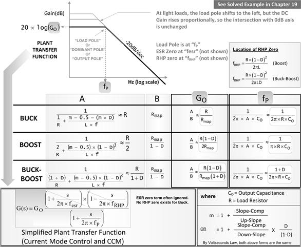
Figure 12.25: Simplified plant transfer function for current-mode control.
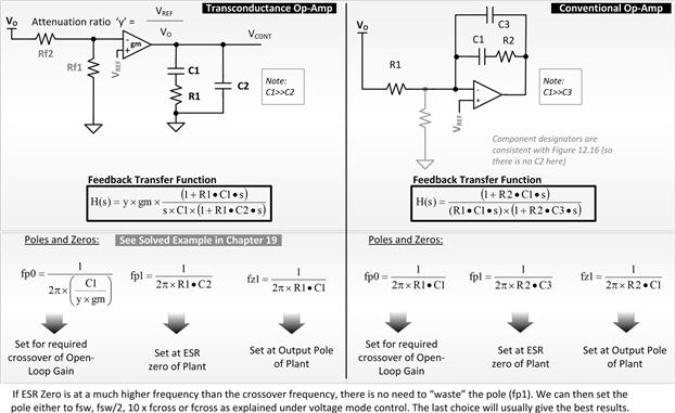
Figure 12.26: Transconductance and conventional type 2 Op-Amp compensation for current-mode control.
The above design procedure is the same for all the topologies. We just have to use the appropriate row of the table provided in Figure 12.25. Note that for all the topologies, the “L” used is now the actual inductance of the converter (not the “equivalent” inductance of the canonical model).
See a full solved example in Chapter 19.