4
COMPUTER ANATOMY

You learned about the properties of bits and ways of using them to represent things in Chapter 1. In Chapters 2 and 3, you learned why we use bits and how they’re implemented in hardware. You also learned about a number of basic building blocks and how they could be combined into more complex configurations. In this chapter, you’ll learn how those building blocks can be combined into a circuit that can manipulate bits. That circuit is called a computer.
There are many ways of constructing a computer. The one we’ll build in this chapter was chosen for ease of explanation, not because it’s the best possible design. And although simple computers work, a lot of additional complexity is required to make them work well. This chapter sticks to the simple computer; the next two chapters cover some of the extra complications.
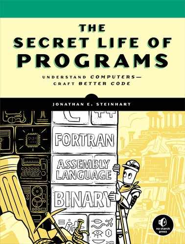
There are three big pieces in a modern computer. These are the memory, the input and output (I/O), and the central processing unit (CPU). This section covers how these pieces relate to each other. Chapter 3 introduced memory, and Chapter 5 covers computers and memory in more detail. I/O is the subject of Chapter 6. The CPU lives in what I’m calling “City Center” in this chapter.
Memory
Computers need someplace to keep the bits that they’re manipulating. That place is memory, as you learned in Chapter 3. Now it’s time to find out how computers use it.
Memory is like a long street full of houses. Each house is exactly the same size and has room for a certain number of bits. Building codes have pretty much settled on 1 byte per house. And just like on a real street, each house has an address, which is just a number. If you have 64 MiB of memory in your computer, that’s 64 × 1,024 × 1,024 = 67,108,864 bytes (or 536,870,912 bits). The bytes have addresses from 0 to 67,108,863. This numbering makes sense, unlike the numbering on many real streets.
It’s pretty common to refer to a memory location, which is just memory at a particular address, such as 3 Memory Lane (see Figure 4-1).

Figure 4-1: Memory Lane
Just because the basic unit of memory is a byte doesn’t mean we always look at it that way. For example, 32-bit computers usually organize their memory in 4-byte chunks, while 64-bit computers usually organize their memory in 8-byte chunks. Why does that matter? It’s like having a four- or eight-lane highway instead of a one-lane road. More lanes can handle more traffic because more bits can get on the data bus. When we address memory, we need to know what we’re addressing. Addressing long words is different from addressing bytes because there are 4 bytes to a long word on a 32-bit computer, and 8 bytes to a long word on a 64-bit computer. In Figure 4-2, for example, long-word address 1 contains byte addresses 4, 5, 6, and 7.
Another way to look at it is that the street in a 32-bit computer contains fourplexes, not single houses, and each fourplex contains two duplexes. That means we can address an individual unit, a duplex, or a whole building.

Figure 4-2: Memory highway
You may have noticed that each building straddles the highway such that each byte has its own assigned lane, and a long word takes up the whole road. Bits commute to and from City Center on a bus that has four seats, one for each byte. The doors are set up so that there’s one seat for each lane. On most modern computers, the bus stops only at one building on each trip from City Center. This means we can’t do things like form a long word from bytes 5, 6, 7, and 8, because that would mean that the bus would have to make two trips: one to building 0 and one to building 1. Older computers contained a complicated loading dock that allowed this, but planners noticed that it wasn’t all that useful and so they cut it out of the budget on newer models. Trying to get into two buildings at the same time, as shown in Figure 4-3, is called a nonaligned access.

Figure 4-3: Aligned and nonaligned accesses
There are lots of different kinds of memory, as we saw in the previous chapter. Each has a different price/performance ratio. For example, SRAM is fast and expensive, like the highways near where the politicians live. Disk is cheap and slow—the dirt road of memory.
Who gets to sit in which seat when commuting on the bus? Does byte 0 or byte 3 get to sit in the leftmost seat when a long word heads into town? It depends on the processor you’re using, because designers have made them both ways. Both work, so it’s pretty much a theological debate. In fact, the term endian—based on the royal edicts in Lilliput and Blefuscu in Jonathan Swift’s Gulliver’s Travels regarding which was the proper end on which to crack open a soft-boiled egg—is used to describe the difference.
Byte 0 goes into the rightmost seat in little-endian machines like Intel processors. Byte 0 goes into the leftmost seat in big-endian machines like Motorola processors. Figure 4-4 compares the two arrangements.

Figure 4-4: Big- and little-endian arrangements
Endianness is something to keep in mind when you’re transferring information from one device to another, because you don’t want to inadvertently shuffle the data. A notable instance of this occurred when the UNIX operating system was ported from the PDP-11 to an IBM Series/1 computer. A program that was supposed to print out “Unix” printed out “nUxi” instead, as the bytes in the 16-bit words got swapped. This was sufficiently humorous that the term nuxi syndrome was coined to refer to byte-ordering problems.
Input and Output
A computer that couldn’t communicate with the outside world wouldn’t be very useful. We need some way to get things in and out of the computer. This is called I/O for input/output. Things that connect to the I/O are called I/O devices. Since they’re on the periphery of the computer, they’re also often called peripheral devices or just peripherals.
Computers used to have a separate I/O avenue, as shown in Figure 4-5, that was similar to Memory Lane. This made sense when computers were physically huge, because they weren’t squeezed into small packages with a limited number of electrical connections. Also, Memory Lane wasn’t very long, so it didn’t make sense to limit the number of addresses just to support I/O.

Figure 4-5: Separate memory and I/O buses
Memory Lane is much longer now that 32- and 64-bit computers are common. It’s so long that there aren’t houses at every address; many empty lots are available. In other words, there are addresses that have no memory associated with them. As a result, it now makes more sense to set aside a portion of Memory Lane for I/O devices. It’s like the industrial district on the edge of town. Also, as more circuitry is crammed into a package that has a limited number of connections, it just makes sense for I/O to be on the same bus as memory.
Many computers are designed with standard input/output slots so that I/O devices can be connected in a uniform manner. This is done sort of like how property was distributed in the Old West; the unincorporated territory is partitioned into a set of land grants, as shown in Figure 4-6. Each slot holder gets the use of all addresses up to its borders. Often there is a specific address in each slot that contains some sort of identifier so that City Center can conduct a census to determine who’s living in each slot.
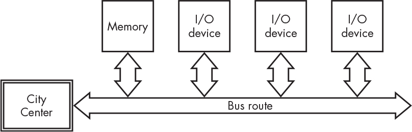
Figure 4-6: Shared memory and I/O bus
We often use a shipping metaphor and say that things are hooked up to I/O ports.
The Central Processing Unit
The central processing unit (CPU) is the part of the computer that does the actual computing. It lives at City Center in our analogy. Everything else is the supporting cast. The CPU is made up of many distinct pieces that we’ll learn about in this section.
Arithmetic and Logic Unit
The arithmetic logic unit (ALU) is one of the main pieces of a CPU. It’s the part that knows how to do arithmetic, Boolean algebra, and other operations. Figure 4-7 shows a simple diagram of an ALU.

Figure 4-7: A sample ALU
The operands are just bits that may represent numbers. The operation code, or opcode, is a number that tells the ALU what operator to apply to the operands. The result, of course, is what we get when we apply the operator to the operands.
The condition codes contain extra information about the result. They are usually stored in a condition code register. A register, which we saw back in Chapter 3, is just a special piece of memory that’s on a different street from the rest of the memory—the street with the expensive, custom homes. A typical condition code register is shown in Figure 4-8. The numbers on top of the boxes are the bit numbers, which is a convenient way to refer to them. Note that some of the bits are not used; this is not unusual.

Figure 4-8: A condition code register
The N is set to 1 if the result of the last operation is a negative number. The Z bit is set to 1 if the result of the last operation is 0. The O bit is set to 1 if the result of the last operation created an overflow or underflow.
Table 4-1 shows what an ALU might do.
Table 4-1: Sample ALU Opcodes
Opcode |
Mnemonic |
Description |
0000 |
clr |
Ignore the operands; make each bit of the result 0 (clear). |
0001 |
set |
Ignore the operands; make each bit of the result 1. |
0010 |
not |
Ignore B; turn 0s from A to 1s and vice versa. |
0011 |
neg |
Ignore B; the result is the two’s complement of A, –A. |
0100 |
shl |
Shift A left by the low 4 bits of B (see next section). |
0101 |
shr |
Shift A right by the low 4 bits of B (see next section). |
0110 |
|
Unused. |
0111 |
|
Unused. |
1000 |
load |
Pass operand B to the result. |
1001 |
and |
The result is A AND B for each bit in the operands. |
1010 |
or |
The result is A OR B for each bit in the operands. |
1011 |
xor |
The result is A XOR B for each bit in the operands. |
1100 |
add |
The result is A + B. |
1101 |
sub |
The result is A – B. |
1110 |
cmp |
Set condition codes based on B – A (compare). |
1111 |
|
Unused. |
The ALU may appear mysterious, but it’s really just some logic gates feeding a selector, which you’ve seen before. Figure 4-9 shows the general design of an ALU, omitting some of the more complicated functions for the sake of simplicity.

Figure 4-9: ALU partial internals
Shiftiness
You may have noticed the shift operations in Table 4-1. A left shift moves every bit left one position, throwing away the leftmost bit and moving a 0 into the vacated rightmost position. If we left-shift 01101001 (10510) by 1, we’ll get 11010010 (21010). This is pretty handy because left-shifting a number one position multiplies it by 2.
A right shift moves every bit right one position, throwing away the rightmost bit and moving a 0 into the vacated leftmost position. If we right-shift 01101001 (10510) by 1, we’ll get 00110100 (5210). This divides a number by 2, throwing away the remainder.
The value of the MSB (most significant bit) lost when left-shifting or the LSB (least significant bit) when right-shifting is often needed, so it’s saved in the condition code register. Let’s make believe that our CPU saves it in the O bit.
You might have noticed that everything in the ALU looks like it can be implemented in combinatorial logic except these shift instructions. You can build shift registers out of flip-flops where the contents are shifted one bit position per clock.
A sequential shift register (shown in Figure 4-10) is slow because it takes one clock per bit in the worst case.

Figure 4-10: A sequential shift register
We can solve this by constructing a barrel shifter entirely out of combinatorial logic using one of our logic building blocks, the selector (refer back to Figure 2-47). To build an 8-bit shifter, we would need eight of the 8:1 selectors.
There is one selector for each bit, as shown in Figure 4-11.

Figure 4-11: A combinatorial barrel shifter
The amount of right shift is provided on S0-2. You can see that with no shift (000 for S), input bit 0 (I0) gets passed to output bit 0 (O0), I1 to O1, and so on. When S is 001, the outputs are shifted right by one because that’s the way the inputs are wired up to the selector. When S is 010, the outputs are shifted right by two, and so on. In other words, we have all eight possibilities wired and just select the one we want.
You may wonder why I keep showing these logic diagrams as if they’re built out of old 7400 series parts. Functions such as gates, multiplexors, demultiplexors, adders, latches, and so on are available as predefined components in integrated circuit design systems. They’re used just like the old components, except instead of sticking lots of the 7400 series parts I mentioned in Chapter 2 onto a circuit board, we now assemble similar components into a single chip using design software.
You may have noticed the absence of multiplication and division operations in our simple ALU. That’s because they’re much more complicated and don’t really show us anything we haven’t already seen. You know that multiplication can be performed by repeated addition; that’s the sequential version. You can also build a combinatorial multiplier by cascading barrel shifters and adders, keeping in mind that a left shift multiplies a number by 2.
Shifters are a key element for the implementation of floating-point arithmetic; the exponents are used to shift the mantissas to line up the binary points so that they can be added together, subtracted, and so on.
Execution Unit
The execution unit of a computer, also known as the control unit, is the boss. The ALU isn’t much use by itself, after all—something has to tell it what to do. The execution unit grabs opcodes and operands from the right places in memory, tells the ALU what operations to perform, and puts the results back in memory. Hopefully, it does all that in an order that serves some useful purpose. (By the way, we’re using the “to perform” definition of execute. No bits are actually killed.)
How might the execution unit do this? We give it a list of instructions, things like “add the number in location 10 to the number in location 12 and put the result in location 14.” Where does the execution unit find these instructions? In memory! The technical name for what we have here is a stored-program computer. It has its genesis in work by English wizard Alan Turing (1912–1954).
That’s right, we have yet another way of looking at bits and interpreting them. Instructions are bit patterns that tell the computer what to do. The bit patterns are part of the design of a particular CPU. They’re not some general standard, like numbers, so an Intel Core i7 CPU would likely have a different bit pattern for the inc A instruction than an ARM Cortex-A CPU.
How does the execution unit know where to look for an instruction in memory? It uses a program counter (often abbreviated PC), which is sort of like a mail carrier, or like a big arrow labeled “You are here.” Shown in Figure 4-12, the program counter is another register, one of those pieces of memory on the special side street. It’s constructed from a counter (see “Counters” on page 77) instead of a vanilla register (see “Registers” on page 78). You can view the counter as a register with additional counting functionality.
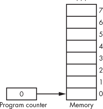
Figure 4-12: A program counter
The program counter contains a memory address. In other words, it points at, or references, a location in memory. The execution unit fetches an instruction from the location referenced by the program counter. There are special instructions that change the value of the program counter, which we’ll see shortly. Unless we’re executing one of these, the program counter is incremented (that is, the size of one instruction is added to it) after the instruction is executed so that the next instruction will come from the next memory location. Note that CPUs have some initial program counter value, usually 0, when the power is turned on. The counter we saw in Figure 3-17 has inputs to support all these functions.
It all works kind of like a treasure hunt. The computer goes to a certain place in memory and finds a note. It reads that note, which tells it to do something, and then goes someplace else to get the next note, and so on.
Instruction Set
The notes that computers find in memory during their treasure hunt are called instructions. This section goes into what those instructions contain.
Instructions
To see what sort of instructions might we find in a CPU, and how we choose bit patterns for them, our example assumes a computer with 16-bit-wide instructions.
Let’s try dividing our instruction into four fields—the opcode plus addresses for two operands and result—as shown in Figure 4-13.

Figure 4-13: Three-address instruction layout
This may seem like a good idea, but it doesn’t work very well. Why? Because we only have room for 4 bits of address for each of the operands and the result. It’s kind of hard to address a useful amount of memory when you have only 16 addresses. We could make the instruction bigger, but even if we went to 64-bit-wide instructions, we’d have only 20 bits of address, which would reach only a mebibyte of memory. Modern machines have gibibytes of memory.
Another approach would be to duplicate the DRAM addressing trick we saw in Figure 3-23. We could have an address extension register and load it with the high-order address bits using a separate instruction. This technique was used by Intel to allow its 32-bit machines to access more than 4-GiB of memory. Intel called it PAE, for physical address extension. Of course, it takes extra time to load this register, and lots of register loads are required if we need memory on both sides of the boundary created by this approach.
There’s an even more important reason why the three-address format doesn’t work well, though: it counts on some magic, nonexistent form of memory that allows three different locations to be addressed at the same time. All three memory blocks in Figure 4-14 are the same memory device; there aren’t three address buses and three data buses.

Figure 4-14: Unworkable computer architecture
We could make this work by having one register hold the contents of operand A and another hold the contents of operand B. The hardware would need to do the following:
- Load the instruction from memory using the address in the program counter.
- Load the operand A register using the address from the operand A portion of the instruction.
- Load the operand B register using the address from the operand B portion of the instruction.
- Store the result in memory using the address from the result portion of the instruction.
That’s a lot of complicated hardware. If each of these steps took a clock cycle, then it would take four cycles just to get something done. We should take a hint from the fact that we can access only one memory location at a time and design our instruction set accordingly. More address bits would be available if we tried to address only one thing at a time.
We can do that by adding another house to the register street. We’ll call this register the accumulator, or A register for short, and it will hold the result from the ALU. Rather than doing an operation between two memory locations, we’ll do it between one memory location and the accumulator. Of course, we’ll have to add a store instruction that stores the contents of the accumulator in a memory location. So now we can lay out our instructions as shown in Figure 4-15.

Figure 4-15: Single-address instruction layout
This gets us more address bits, but it takes more instructions to get things done. We used to be able to have an instruction that said:
C = A + B
But now we need three instructions:
Accumulator = A
Accumulator = Accumulator + B
C = Accumulator
You might notice that we just replaced one instruction with three, effectively making the instruction bigger and contradicting ourselves. That’s true for this simple case, but it’s not true in general. Let’s say we needed to calculate this:
D = A + B + C
We couldn’t do that in a single instruction even if it could access three addresses because now we need four. We’d have to do it like this:
Intermediate = A + B
D = Intermediate + C
Sticking with 12 bits of address, we’d need 40-bit instructions to handle three address plus the opcode. And we’d need two of these instructions for a total of 80 bits to calculate D. Using the single-address version of the instructions requires four instructions for a total of 64 bits.
Accumulator = A
Accumulator = Accumulator + B
Accumulator = Accumulator + C
D = Accumulator
Addressing Modes
Using an accumulator managed to get us 12 address bits, and although being able to address 4,096 bytes is much better than 16, it’s still not enough. This way of addressing memory is known as direct addressing, which just means that the address is the one given in the instruction.
We can address more memory by adding indirect addressing. With indirect addressing, we get the address from the memory location contained in the instruction, rather than directly from the instruction itself. For example, let’s say memory location 12 contains the value 4,321, and memory location 4,321 contains 345. If we used direct addressing, loading from location 12 would get 4,321, while indirect addressing would get 345, the contents of location 4,321.
This is all fine for dealing with memory, but sometimes we just need to get constant numbers. For example, if we need to count to 10, we need some way of loading that number. We can do this with yet another addressing mode, called immediate mode addressing. Here the address is just treated as a number, so, using the previous example, loading 12 in immediate mode would get 12. Figure 4-16 compares these addressing modes.

Figure 4-16: Addressing modes
Clearly, direct addressing is slower than immediate addressing as it takes a second memory access. Indirect is slower still as it takes a third memory access.
Condition Code Instructions
There are still a few things missing from our CPU, such as instructions that work with the condition codes. We’ve seen that these codes are set by addition, subtraction, and comparison. But we need some way of setting them to known values and some way of looking at the values. We can do that by adding a cca instruction that copies the contents of the condition code register to the accumulator and an acc instruction that copies the contents of the accumulator to the condition code register.
Branching
Now we have instructions that can do all sorts of things, but all we can do is execute a list of them from start to finish. That’s not all that useful. We’d really like to have programs that can make decisions and select portions of code to execute. Those would take instructions that let us change the value of the program counter. These are called branch instructions, and they cause the program counter to be loaded with a new address. By itself, that’s not any more useful than just being able to execute a list of instructions. But branch instructions don’t always branch; they look at the condition codes and branch only if the conditions are met. Otherwise, the program counter is incremented normally, and the instruction following the branch instruction is executed next. Branch instructions need a few bits to hold the condition, as shown in Table 4-2.
Table 4-2: Branch Instruction Conditions
Code |
Mnemonic |
Description |
000 |
bra |
Branch always. |
001 |
bov |
Branch if the O (overflow) condition code bit is set. |
010 |
beq |
Branch if the Z (zero) condition code bit is set. |
011 |
bne |
Branch if the Z condition code bit is not set. |
100 |
blt |
Branch if N (negative) is set and Z is clear. |
101 |
ble |
Branch if N or Z is set. |
110 |
bgt |
Branch if N is clear and Z is clear. |
111 |
bge |
Branch if N is clear or Z is set. |
Sometimes we need to explicitly change the contents of the program counter. We have two special instructions to help with this: pca, which copies the current program counter value to the accumulator, and apc, which copies the contents of the accumulator to the program counter.
Final Instruction Set
Let’s integrate all these features into our instruction set, as shown in Figure 4-17.

Figure 4-17: The final instruction layout
We have three addressing modes, which means that we need 2 bits in order to select the mode. The unused fourth-bit combination is used for operations that don’t involve memory.
The addressing mode and opcode decode into instructions, as you can see in Table 4-3. Note that the branch conditions are merged into the opcodes. The opcodes for addressing mode 3 are used for operations that involve only the accumulator. A side effect of the complete implementation is that the opcodes don’t exactly match the ALU that we saw in Table 4-1. This is not unusual and requires some additional logic.
Table 4-3: Addressing Modes and Opcodes
Opcode |
Addressing mode |
|||
Direct (00) |
Indirect (01) |
Immediate (10) |
None (11) |
|
0000 |
load |
load |
load |
|
0001 |
and |
and |
and |
set |
0010 |
or |
or |
ore |
not |
0011 |
xor |
xor |
xor |
neg |
0100 |
add |
add |
add |
shl |
0101 |
sub |
sub |
sub |
shr |
0110 |
cmp |
cmp |
cmp |
acc |
0111 |
store |
store |
|
cca |
1000 |
bra |
bra |
bra |
apc |
1001 |
bov |
bov |
bov |
pca |
1010 |
beq |
beq |
beq |
|
1011 |
bne |
bne |
bne |
|
1100 |
blt |
blt |
blt |
|
1101 |
ble |
bge |
ble |
|
1110 |
bgt |
bgt |
bgt |
|
1111 |
bge |
bge |
bge |
|
The shift-left and shift-right instructions put some of the otherwise unused bits to use as a count of the number of positions to shift, as shown in Figure 4-18.

Figure 4-18: Shift instruction layout
Now we can actually instruct the computer to do something by writing a program, which is just a list of instructions that carry out some task. We’ll compute all Fibonacci (Italian mathematician, 1175–1250) numbers up to 200. Fibonacci numbers are pretty cool; the number of petals on flowers, for example, are Fibonacci numbers. The first two Fibonacci numbers are 0 and 1. We get the next one by adding them together. We keep adding the new number to the previous one to get the sequence, which is 0, 1, 1, 2, 3, 5, 8, 13, and so on. The process looks like Figure 4-19.

Figure 4-19: Flowchart for Fibonacci sequence program
The short program shown in Table 4-4 implements this process. The Instruction column is divided into fields as per Figure 4-17. The addresses in the comments are decimal numbers.
Table 4-4: Machine Language Program to Compute Fibonacci Sequence
Address |
Instruction |
Description |
0000 |
10 0000 0000000000 |
Clear the accumulator (load 0 immediate). |
0001 |
00 0111 0001100100 |
Store the accumulator (0) in memory location 100. |
0010 |
10 0000 0000000001 |
Load 1 into the accumulator (load 1 immediate). |
0011 |
00 0111 0001100101 |
Store the accumulator (1) in memory location 101. |
0100 |
00 0000 0001100100 |
Load the accumulator from memory location 100. |
0101 |
10 0100 0001100101 |
Add the contents of memory location 101 to the accumulator. |
0110 |
00 0111 0001100110 |
Store the accumulator in memory location 102. |
0111 |
00 0000 0001100101 |
Load the accumulator from memory location 101. |
1000 |
00 0111 0001100100 |
Store it in memory location 100. |
1001 |
00 0000 0001100110 |
Load the accumulator from memory location 102. |
1010 |
00 0111 0001100101 |
Store it in memory location 101. |
1011 |
10 0110 0011001000 |
Compare the contents of the accumulator to the number 200. |
1100 |
00 0111 0000000100 |
Do another number if the last one was less than 200 by branching to address 4 (0100). |
The Final Design
Let’s put all the pieces that we’ve seen so far together into an actual computer. We’ll need a few pieces of “glue” to make it all work.
The Instruction Register
You might be fooled into thinking that the computer just executes the Fibonacci program one instruction at a time. But more is happening behind the scenes. What does it take to execute an instruction? There’s a state machine doing the two-step, shown in Figure 4-20.

Figure 4-20: The fetch-execute cycle
The first thing that we have to do is to fetch an instruction from memory. Once we have that instruction, then we can worry about executing it.
Executing instructions usually involves accessing memory. That means we need someplace to keep the instruction handy while we’re using memory for some other task. In Figure 4-21, we add an instruction register to our CPU to hold the current instruction.

Figure 4-21: Adding an instruction register
Data Paths and Control Signals
Here comes the complicated part. We need a way to feed the contents of the program counter to the memory address bus and a way to feed the memory data into the instruction register. We can do a similar exercise to determine all the different connections required to implement everything in our instruction set as detailed in Table 4-4. We end up with Figure 4-22, which probably seems confusing. But it’s really just things we’ve seen before: some registers, some selectors, the ALU, and a tri-state buffer.
Although this looks pretty complicated, it’s just like a road map. And it’s way simpler than a real city map. The address selector is just a three-way intersection, and the data selector is a four-way. There are connections hanging off of the address bus and data bus for things like the I/O devices that we’ll discuss in Chapter 6.
Figure 4-22: Data paths and control signals
The only new part is the indirect address register. We need that because we need somewhere to hold indirect addresses fetched from memory, similar to how the instruction register holds instructions fetched from memory.
For simplicity, Figure 4-22 omits the system clock that goes to all of the registers and memory. In the simple register case, just assume the register is loaded on the next clock if enabled. Likewise, the program counter and memory do what their control signals tell them to do on each clock. All the other components, such as the selectors, are purely combinatorial and don’t use the clock.
Traffic Control
Now that you’re familiar with all the inputs and outputs, it’s time to build our traffic control unit. Let’s look at a couple of examples of how it needs to behave.
Fetching is common to all instructions. The following signals are involved:
- The address source must be set to select the program counter.
- The memory must be enabled, and the read-write signal r/ must be set to read (1).
- The instruction register must be enabled.
For our next example, we’ll store the contents of the accumulator at the memory address pointed to by the address contained in the instruction—in other words, using indirect addressing. Fetching works as before.
Get the indirect address from memory:
- The address source must be set to select the instruction register, which gets us the address portion of the instruction.
- Memory is enabled, and r/ is set to read (1).
- The indirect address register is enabled.
Store the accumulator in that address:
- The address source must be set to select the indirect address register.
- The data bus enable must be set.
- Memory is enabled and r/ is set to write (0).
- The program counter is incremented.
Since multiple steps are involved in fetching and executing instructions, we need a counter to track them. The counter contents plus the opcode and mode portions of the instruction are all we need to generate all the control signals. We need 2 bits of counter because three states are needed to execute our most complicated instructions, as illustrated in Figure 4-23.

Figure 4-23: Random logic traffic control
This is a big box full of what’s called random logic. All the logic diagrams we’ve seen so far follow some regular pattern. Functional blocks, such as selectors and registers, are assembled from simpler blocks in a clear manner. Sometimes, such as when we’re implementing our traffic control unit, we have a set of inputs that must be mapped to a set of outputs to accomplish a task that has no regularity. The schematic looks like a rat’s nest of connections—hence the descriptor “random.”
But there’s another way we could implement our traffic control unit. Instead of random logic, we could use a hunk of memory. The address would be formed from the counter outputs plus the opcode and mode portions of the instruction, as shown in Figure 4-24.

Figure 4-24: Memory-based traffic control
Each 19-bit memory word is laid out as shown in Figure 4-25.
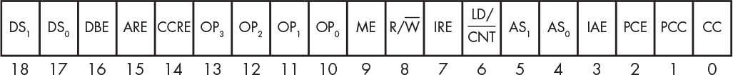
Figure 4-25: The layout of a microcode word
This might strike you as somewhat strange. On the one hand, it’s just another state machine implemented using memory instead of random logic. On the other, it sure looks like a simple computer. Both interpretations are correct. It is a state machine because computers are state machines. But it is also a computer because it’s programmable.
This type of implementation is called microcoded, and the contents of memory are called microcode. Yes, we’re using a small computer as part of the implementation of our larger one.
Let’s look at the portion of the microinstructions, shown in Figure 4-26, that implement the examples we’ve discussed.

Figure 4-26: Microcode example
As you might expect, it’s hard to avoid abusing a good idea. There are machines that have a nanocoded block that implements a microcoded block that implements the instruction set.
Using ROM for the microcode memory makes a certain amount of sense, because otherwise we’d need to keep a copy of the microcode somewhere else and we’d require additional hardware to load the microcode. However, there are situations where RAM, or a mix of ROM and RAM, is justified. Some Intel CPUs have writable microcode that can be patched to fix bugs. A few machines, such as the HP-2100 series, had a writable control store, which was microcode RAM that could be used to extend the basic instruction set.
Machines that have writable microcode today rarely permit users to modify it for several reasons. Manufacturers don’t want users to rely on microcode they themselves write for their applications because once users become dependent on it, manufacturers have difficulty making changes. Also, buggy microcode can damage the machine—for example, it could turn on both the memory enable and data bus enable at the same time in our CPU, connecting together totem-pole outputs in a way that might burn out the transistors.
RISC vs. CISC Instruction Sets
Designers used to create instructions for computers that seemed to be useful but that resulted in some pretty complicated machines. In the 1980s, American computer scientists David Patterson at Berkeley and John Hennessey at Stanford did statistical analyses of programs and discovered that many of the complicated instructions were rarely used. They pioneered the design of machines that contained only the instructions that accounted for most of a program’s time; less used instructions were eliminated and replaced by combinations of other instructions. These were called RISC machines, for reduced instruction set computers. Older designs were called CISC machines, for complicated instruction set computers.
One of the hallmarks of RISC machines is that they have a load-store architecture. This means there are two categories of instructions: one for accessing memory and one for everything else.
Of course, computer use has changed over time. Patterson and Hennessey’s original statistics were done before computers were commonly used for things like audio and video. Statistics on newer programs are prompting designers to add new instructions to RISC machines. Today’s RISC machines are actually more complicated than the CISC machines of yore.
One of the CISC machines that had a big impact was the PDP-11 from Digital Equipment Corporation. This machine had eight general-purpose registers instead of the single accumulator we used in our example. These registers could be used for indirect addressing. In addition, autoincrement and autodecrement modes were supported. These modes enabled the values in the registers to be incremented or decremented before or after use. This allowed for some very efficient programs. For example, let’s say we want to copy n bytes of memory starting at a source address to memory starting at a destination address. We can put the source address in register 0, the destination in register 1, and the count in register 2. We’ll skip the actual bits here because there’s no real need to learn the PDP-11 instruction set. Table 4-5 shows what these instructions do.
Table 4-5: PDP-11 Copy Memory Program
Address |
Description |
0 |
Copy the contents of the memory location whose address is in register 0 to the memory location whose address is in register 1, then add 1 to each register. |
1 |
Subtract 1 from the contents of register 2 and then compare the result to 0. |
2 |
Branch to location 0 if the result was not 0. |
Why should we care about this? The C programming language, a follow-on to B (which was a follow-on to BCPL), was developed on the PDP-11. C’s use of pointers, a higher-level abstraction of indirect addressing, combined with features from B such as the autoincrement and autodecrement operators, mapped well to the PDP-11 architecture. C became very influential and has affected the design of many other languages, including C++, Java, and JavaScript.
Graphics Processing Units
You’ve probably heard about graphics processing units, or GPUs. These are mostly outside the scope of this book but are worth a quick mention.
Graphics is a massive paint-by-numbers exercise. It’s not uncommon to have 8 million color spots to paint and need to paint them 60 times per second if you want video to work well. That works out to around a half-billion memory accesses per second.
Graphics is specialized work and doesn’t require all the features of a general-purpose CPU. And it’s something that parallelizes nicely: painting multiple spots at a time can improve performance.
Two features distinguish GPUs. First, they have large numbers of simple processors. Second, they have much wider memory buses than CPUs, which means they can access memory much faster. GPUs have a fire hose instead of a garden hose.
GPUs have acquired more general-purpose features over time. Work has been done to make them programmable using variants of standard programming languages, and they are now used for certain classes of applications that can take advantage of their architectures. GPUs were in short supply when this book was written because they were all being snapped up for Bitcoin mining.
Summary
In this chapter, we’ve created an actual computer using the building blocks introduced in previous chapters. Though simple, the machine we designed in this chapter could actually be built and programmed. It’s missing some elements found in real computers, however, such as stacks and memory management hardware. We’ll learn about those in Chapter 5.