2
Semiconductor Physics
- 2.1 Introduction
- 2.2 The Band Theory of Solids
- 2.3 Bloch Functions
- 2.4 The Kronig–Penney Model
- 2.5 The Bragg Model
- 2.6 Effective Mass
- 2.7 Number of States in a Band
- 2.8 Band Filling
- 2.9 Fermi Energy and Holes
- 2.10 Carrier Concentration
- 2.11 Semiconductor Materials
- 2.12 Semiconductor Band Diagrams
- 2.13 Direct Gap and Indirect Gap Semiconductors
- 2.14 Extrinsic Semiconductors
- 2.15 Carrier Transport in Semiconductors
- 2.16 Equilibrium and Non‐Equilibrium Dynamics
- 2.17 Carrier Diffusion and the Einstein Relation
- 2.18 Quasi‐Fermi Energies
- 2.19 The Diffusion Equation
- 2.20 Traps and Carrier Lifetimes
- 2.21 Alloy Semiconductors
- 2.22 Summary
- References
- Further Reading
- Problems
2.1 Introduction
A fundamental understanding of electron behaviour in crystalline solids is available using the band theory of solids. This theory explains a number of fundamental attributes of electrons in solids including:
- concentrations of charge carriers in semiconductors;
- electrical conductivity in metals and semiconductors;
- optical properties such as absorption and photoluminescence;
- properties associated with junctions and surfaces of semiconductors and metals.
The aim of this chapter is to present the theory of the band model and then to exploit it to describe the important electronic properties of semiconductors. This is essential for a proper understanding of p–n junction devices, which constitute both the photovoltaic (PV) solar cell and the light‐emitting diode (LED).
2.2 The Band Theory of Solids
There are several ways of explaining the existence of energy bands in crystalline solids. The simplest picture is to consider a single atom with its set of discrete energy levels for its electrons. The electrons occupy a set of quantum states with quantum numbers n, l, m, and s denoting the energy level, orbital, and spin state of the electrons. Now if a number N of identical atoms are brought together in very close proximity as in a crystal, there is some degree of spatial overlap of the outer electron orbitals. This means that there is a chance that any pair of these outer electrons from adjacent atoms could trade places. The Pauli exclusion principle, however, requires that each electron occupy a unique energy state. Satisfying the Pauli exclusion principle becomes an issue because electrons that trade places effectively occupy new, spatially extended energy states.
In fact, since outer electrons from adjacent atoms may trade places, outer electrons from all the atoms may effectively trade places with each other, and therefore, a set of outermost electrons from the N atoms all appear to share a spatially extended energy state that extends through the entire crystal. The Pauli exclusion principle can only be satisfied if these electrons occupy a set of distinct, spatially extended energy states. This leads to a set of slightly different energy levels for the electrons that all originated from the same atomic orbital. We say that the atomic orbital splits into an energy band containing a large but finite set of electron states with closely spaced energy levels. Additional energy bands will exist if there is some degree of spatial overlap of the atomic electrons in lower‐lying atomic orbitals. This results in a set of energy bands in the crystal. Electrons in the lowest‐lying atomic orbitals will remain virtually unaltered since there is virtually no spatial overlap of these electrons in the crystal.
Figure 2.1 shows a one‐dimensional crystal lattice having lattice constant a on the x ‐axis. The potential energy U(x) experienced by an electron in the crystal is principally controlled by atomic nuclear charges, bound atomic electrons, and electrons involved in bonds. For example, in a covalently bonded crystal, positively charged atomic sites provide potential valleys to a mobile electron and negatively charged regions where covalent bonding electrons are concentrated provide potential barriers. Because the lattice potential energy repeats according to the lattice constant, U(x) is known as a periodic potential energy.
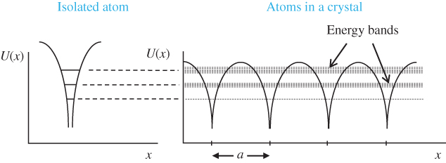
Figure 2.1
The energy levels of a single atom are shown on the left. Once these atoms form a crystal, their proximity causes energy level splitting. The resulting sets of closely spaced energy levels are known as energy bands shown on the right. The electrons in the crystal exist in a periodic potential energy  that has a period equal to the lattice constant a as shown
The picture we have presented is conceptually a very useful one, and it suggests that electrical conductivity may arise in a crystal due to the formation of spatially extended electron states. It does not, however, directly allow us to quantify and understand important aspects of these electrons. We now need to understand the number and the behaviour of the electrons that move about in the solid to determine the electrical properties of semiconductors and other materials in semiconductor devices.
The quantitative description of these spatially extended electrons requires the use of wave functions that describe their spatial distribution as well as their energy and momentum. These wave functions may be obtained by applying Schrödinger's equation to the electrons within a periodic potential energy. The following sections present the resulting band theory of crystalline solids and the results.
2.3 Bloch Functions
There is an important constraint on the wave functions that can exist for an electron experiencing a periodic potential energy. This constraint comes about from the consideration of the periodicity of the crystal. We will assume an infinitely large crystal. Later, in Section 2.7, we will look at the effects of finite crystal dimensions.
It is very difficult to calculate full wave function solutions to Schrödinger's equation for a periodic potential energy. We will therefore start by assuming that ψ(x) is a valid solution to Schrödinger's equation for a periodic potential energy U(x) in one dimension with lattice constant a such as that shown in Figure 2.1. Since we do not have an expression for ψ(x), we will write it in terms of a Fourier series that expresses an arbitrary wave function. A summation of component plane waves is made, each wave having a unique wavelength. We can write
Note that we previously made use of a Fourier series. See Section 1.6 and Appendix 2. The component waves are ![]() , and the Fourier coefficients are
a
n
. As in Example 1.5, each wave component is the spatial part of a travelling plane wave with time dependence given by e
iωt
. We will focus on the spatial part of the wave function.
, and the Fourier coefficients are
a
n
. As in Example 1.5, each wave component is the spatial part of a travelling plane wave with time dependence given by e
iωt
. We will focus on the spatial part of the wave function.
We can also express an arbitrary periodic potential energy U(x) such as that shown in Figure 2.1 by a Fourier series, and we can write
in which the Fourier coefficients are U m . Since U(x) is periodic with period equal to lattice constant a , we know that the wave components of this Fourier series must have specific wavelengths λ m such that the lattice constant a is an integer multiple of λ m . Hence,
U(x) is composed from a fundamental component (m = 1) with harmonics (m ≥ 2) and wave number
K
m
is restricted to values ![]() .
.
Note that we have omitted the term for m = 0, which means that we are neglecting to include non‐zero average potential energy. This is justifiable since in Section 2.4 it will become clear that we are interested in a relative, rather than absolute, energy scale.
The Fourier series expressions in Eqs. 2.1 and 2.2 may now be substituted into the time‐independent Schrödinger equation (Eq. (1.10))
and we obtain
or,
and finally
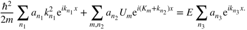
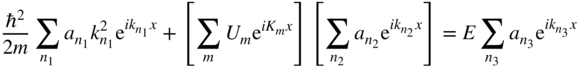
We see that there are three summations, each of which represents a Fourier series of component waves. We are free to assign to each Fourier series its own independent index, and to make this clear, we have labelled the index variables n with subscripts 1, 2, and 3 on the three summations.
We will now seek solutions to Eq. (2.3). Let us select one term in the first summation having wave number ![]() with one specific integer value of index n
1. We now require that
with one specific integer value of index n
1. We now require that
because we cannot express a wave of infinite spatial extent having a given wave number in terms of a Fourier series of waves having other wave numbers that do not include the given wave number. We say that the terms in a Fourier series are orthogonal to each other.
In order for Eq. 2.4 to be satisfied, we need to choose a value of
n
2 ≠ n
1 = n
3
. The smallest value of
K
m
is ![]() for
m = 1. In this case, we could satisfy Eq. 2.4 by making
for
m = 1. In this case, we could satisfy Eq. 2.4 by making ![]() . The next available term in the Fourier series for
U(x) has
. The next available term in the Fourier series for
U(x) has ![]() , and Eq. 2.4 could be satisfied if
, and Eq. 2.4 could be satisfied if ![]() . As we extend this analysis to higher order terms of
U(x), we discover that adjacent terms of
ψ(x) must have wave numbers that are separated by
. As we extend this analysis to higher order terms of
U(x), we discover that adjacent terms of
ψ(x) must have wave numbers that are separated by ![]() , and we realise that allowable forms of
ψ(x) that satisfy Eq. (2.4) are restricted to summations that may be written
, and we realise that allowable forms of
ψ(x) that satisfy Eq. (2.4) are restricted to summations that may be written
where the first term in the summation contains ![]() and
n = n
1 = n
3
.
and
n = n
1 = n
3
. ![]() is the fundamental wave number of the Fourier series representation of
U(x), and adjacent terms have wave numbers that are separated by
is the fundamental wave number of the Fourier series representation of
U(x), and adjacent terms have wave numbers that are separated by ![]() . Each term has a distinct value of its resulting wave number k
n − K
m and each term will therefore result in a distinct electron energy E in Schrödinger's equation. This set of uniformly spaced and discrete wave numbers and associated energies for our selected wave number
. Each term has a distinct value of its resulting wave number k
n − K
m and each term will therefore result in a distinct electron energy E in Schrödinger's equation. This set of uniformly spaced and discrete wave numbers and associated energies for our selected wave number ![]() will be shown to correspond to energy bands in Section 2.5.
will be shown to correspond to energy bands in Section 2.5.
We can repeat this analysis for other values of kn each having a unique integer value of n. This leads directly to the result that the allowed wave functions for the periodic potential must be of the form
where
Summation un (x) must have the same periodicity as the periodic potential U(x) because it contains wave components that have the same wave numbers as the periodic potential. In addition, the first term in the summation of terms of un (x) has the fundamental wave number of the Fourier series representation of U(x). We can now state Bloch's theorem: Electrons in a periodic potential energy U(x) must have wave functions called Bloch functions expressed as ψ(x) = u(x)e ikx , where u(x) has the same periodicity as the periodic potential energy.
A Bloch function contains the spatial part of a travelling wave e ikx modulated by u(x). The wave may travel in either direction along the x‐axis depending on the sign of wave number k . The choice of k for the wave number is consistent with the notion of a crystal wave number for an electron travelling through a periodic potential in a crystal.
The Bloch function is very general in that the form of the periodic potential is not specified and the crystal is assumed to be infinite in length. Our understanding of Bloch functions will improve as we further investigate the properties of electrons in periodic potentials in Sections 2.4 and 2.5.
We have derived Bloch's theorem in one dimension. The derivation in three dimensions is very similar. See Suggestions for Further Reading.
2.4 The Kronig–Penney Model
The Kronig–Penney model builds on Bloch functions and is able to further explain the essential features of band theory. First, consider an electron that exists in a specific one‐dimensional periodic potential energy U(x). The periodic potential energy can be approximated by a series of regions having zero potential energy separated by potential energy barriers of height U 0 and width b as shown in Figure 2.2, resulting in a periodic potential energy with period a + b . We will assume an infinite number of potential energy barriers extending over the range − ∞ < x < ∞. We associate a + b with the lattice constant of the crystal. Note that the electric potential energy in a real crystal such as that represented in Figure 2.1 is different from the idealised shape of this periodic potential energy; however, the result turns out to be relevant in any case, and Schrödinger's equation is much easier to solve starting from the U(x) of Figure 2.2.
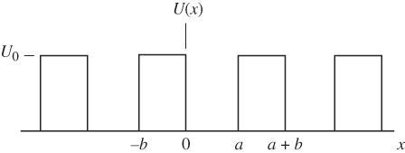
Figure 2.2
Periodic one‐dimensional potential energy  used in the Kronig–Penney model
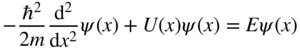
We now take U(x) from Figure 2.2 as well as the Bloch functions from Eq. 2.5 and apply them to the time‐independent Schrödinger equation (Eq. (1.10)) in one dimension. Hence,
or
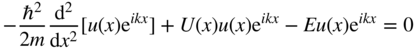
Now, consider regions along the x‐axis for which U(x) = 0. The solutions in these regions will be designated ψ 1 = u 1(x)e ikx , and we have
or
and hence,

If we define ![]() , then this can be written as
, then this can be written as
Note that our use of variable K here is distinct from its use in Section 2.3. Now, consider regions along the x‐axis in which U(x) = U 0 . The solutions in these regions will be designated ψ 2 = u 2(x)e ikx , and using the same approach, we obtain
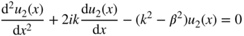
where we define ![]() . Note that if
E > U
0
, then
β
is a real number, and if
E < U
0, then
β
is an imaginary number.
. Note that if
E > U
0
, then
β
is a real number, and if
E < U
0, then
β
is an imaginary number.
Solutions to Eqs. 2.7 and 2.8 are
and
respectively. Note that we have been focusing on selected regions of the x‐axis. To satisfy Schrödinger's equation for all values of
x
, both
ψ
1
and
ψ
2
, and hence
u
1
and
u
2
, must be continuous, and their first derivatives must also be continuous. At
x = 0, we require that
u
1 = u
2
and that ![]() . From Eqs. 2.9 and 2.10, this gives us
. From Eqs. 2.9 and 2.10, this gives us
and
In addition, the Bloch theorem requires that
u(x) is periodic with period equal to that of U(x). Hence, we can state that
u
1(a) = u
2(−b) and that ![]() . From Eqs. 2.9 and 2.10, this gives us
. From Eqs. 2.9 and 2.10, this gives us
and
Equations 2.9 2.10 2.11 2.12 constitute four equations with four unknowns A, B, C, and D. Solutions exist only if the determinant of the coefficients of A, B, C, and D is zero (Cramer's rule) (see Problem 2.1). The result is that
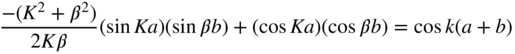
We will now choose the cases in which total electron energy E < U 0 for which β is an imaginary number. This is seen to best represent Figure 2.1 in which U(x) is larger than E in periodic portions of the x‐axis. Let us define β = iγ, where γ is a real number. Equation 2.13 may now be rewritten as
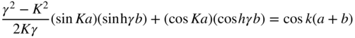
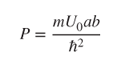
This may be simplified if the limits b → 0 and U 0 → ∞ are taken such that bU 0 is constant (see Problem 2.2). We now define
Since γ > K and γ b ≪ 1, using Eq. 2.14, we obtain
Here, k is the wave number of the electron in the periodic potential and
which means that K is a term associated with the electron's energy.
Equation 2.15 only has solutions if its right‐hand side is between −1 and +1, which restricts the possible values of Ka. The right‐hand side is plotted as a function of Ka in Figure 2.3.
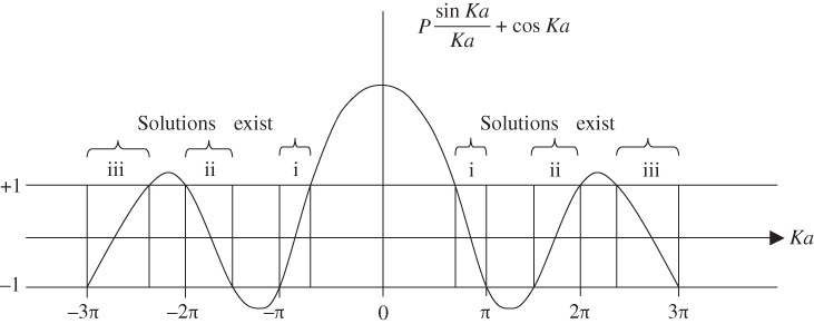
Figure 2.3
Graph of right‐hand side of Eq. 2.14 as a function of  for
for 
Since K and E are related by Eq. 2.15, these allowed ranges of Ka actually describe energy bands (allowed ranges of E) separated by energy gaps or band gaps (forbidden ranges of E). Ka may be re‐plotted on an energy axis, which is related to the Ka axis by the square‐root relationship of Eq. 2.16. It is convenient to view E on a vertical axis and
k
on a horizontal axis as shown in Figure 2.4. Note that ![]() , with
n
an integer, at the highest and lowest points of each energy band where the left side of Eq. 2.15 is equal to ±1. These critical values of k occur at Brillouin zone boundaries, and the remaining values of
k
lie within Brillouin zones. Figure 2.4 clearly shows the energy bands and energy gaps. Also, it is seen that
k
may be positive or negative to denote the direction of motion of an electron along the x‐axis. For this reason, we should view
k
as a wave vector
k
, although we will continue to refer to it as a wave number with both positive and negative values. Note that only three of many energy bands are illustrated.
, with
n
an integer, at the highest and lowest points of each energy band where the left side of Eq. 2.15 is equal to ±1. These critical values of k occur at Brillouin zone boundaries, and the remaining values of
k
lie within Brillouin zones. Figure 2.4 clearly shows the energy bands and energy gaps. Also, it is seen that
k
may be positive or negative to denote the direction of motion of an electron along the x‐axis. For this reason, we should view
k
as a wave vector
k
, although we will continue to refer to it as a wave number with both positive and negative values. Note that only three of many energy bands are illustrated.
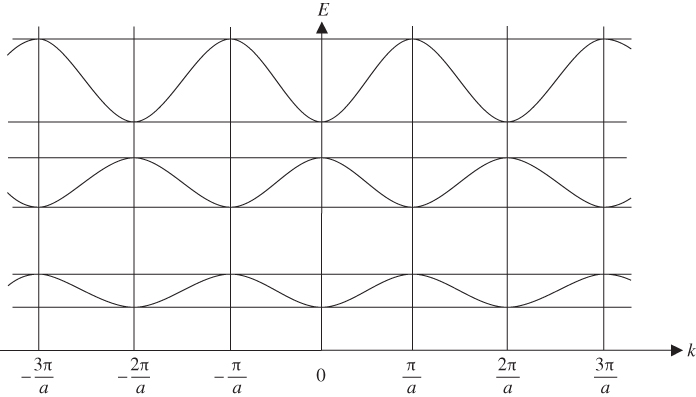
Figure 2.4
Plot of  versus
  showing how
  varies within each energy band and the existence of energy bands and energy gaps. The vertical lines at
  are Brillouin zone boundaries. The first Brillouin zone extends from
  , and the second Brillouin zone includes both
  (negative wave numbers) and
  (positive wave numbers)
Let us now consider an electron not inside a periodic potential, but instead in a one‐dimensional space with zero potential energy. Solving Eq. (1.10) for a free electron with U = 0 as shown in Example 1.5 yields the solution
where
This parabolic E versus k relationship may be plotted superimposed on the curves from Figure 2.4. The result is shown in Figure 2.5.
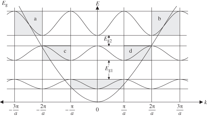
Figure 2.5
Plot of  versus
  comparing the result of the Kronig–Penney model to the free electron parabolic result
Taking the limit P → 0, and combining Eqs. 2.15 and 2.16, we obtain:
which is identical to Eq. 2.17. This means that the dependence of E on k shown in Figure 2.5 will become parabolic if the amplitude of the periodic potential energy is reduced to zero.
The important relationship between the parabola and the Kronig–Penney model is evident if we look at the solutions to Eq. 2.15 within the shaded regions in Figure 2.5. We can picture these regions as portions of the free electron parabola that have been broken up by energy gaps and distorted in shape. If the periodic potential energy is weakened, the solutions to Eq. 2.15 more closely resemble the parabola of Eq. (2.17).
We refer to the plots of E versus k in the shaded regions of Figure 2.5 as dispersion relations for electrons in a periodic potential energy. The concept of a dispersion relation was introduced in Section 1.5.
At this point, we can draw some very useful conclusions based on the results of the Kronig–Penney model. The size of the energy gaps increases as the periodic potential energy increases in amplitude in a crystalline solid. Hence:
- The periodic potential energies and energy gaps are larger in amplitude for crystalline semiconductors that have small atoms since there are then fewer atomically bound electrons to screen the point charges of the nuclei of the atoms. In contrast, periodic potential energies and energy gaps are smaller in amplitude for crystalline semiconductors that have large atoms with more electron screening.
- The periodic potential energies and hence energy gaps increase in amplitude for ionic semiconductors compared to covalent semiconductors since the ionic character of the crystal bonding increases the localisation of positive and negative charges along the x‐axis. This will be illustrated in Section 2.11 for some real semiconductors.
To extend our understanding of energy bands, we now need to turn to another picture of electron behaviour in a crystal.
2.5 The Bragg Model
Since electrons behave like waves, they will exhibit the behaviour of waves that undergo reflections. Notice that in a crystal with lattice constant a, the Brillouin zone boundaries occur at wave numbers
and therefore
The well‐known Bragg condition relevant to electromagnetic waves (X‐rays) that undergo strong reflections when incident on a crystal with lattice constant a is
Now, if the electron is treated as such a wave incident at θ = 90°, we have
which is precisely the case at Brillouin zone boundaries. We therefore make the following observation: Brillouin zone boundaries occur at the electron wavelengths that satisfy the requirement for strong reflections from crystal lattice planes according to the Bragg condition. This is not really a surprise since both electrons and photons exhibit wave properties as discussed in detail in Chapter 1.
The free electron parabola in Figure 2.5 is most similar to the Kronig–Penney model well away from Brillouin zone boundaries; however, as we approach Brillouin zone boundaries, strong deviations take place and energy gaps are observed.
There is therefore a fundamental connection between the Bragg condition and the formation of energy gaps. Electrons that satisfy the Bragg condition for a given value of n actually exist as standing waves at a corresponding Brillouin zone boundary. For these electrons, reflections will occur equally for electrons travelling in both directions of the x‐axis. Provided electrons have wavelengths not close to the Bragg condition, they interact relatively weakly with the crystal lattice and behave more like free electrons.
The E versus k dependence immediately above and immediately below a particular energy gap is contained in four of the shaded regions in Figure 2.5 that we discussed in Section 2.4. The shaded regions relevant to E
g2 in Figure 2.5 are labelled a, b, c, and d. These four regions are redrawn in Figure 2.6. Note that each region is shifted along the
k
‐axis by an amount ![]() . In Figure 2.5, energy gap E
g2 occurs at
. In Figure 2.5, energy gap E
g2 occurs at ![]() . Since this is a standing wave condition with electron velocity and electron momentum p = ℏk equal to zero, E
g2 is redrawn at k = 0 in Figure 2.6. Figure 2.6 is known as a reduced zone scheme, and only the first Brillouin zone is shown.
. Since this is a standing wave condition with electron velocity and electron momentum p = ℏk equal to zero, E
g2 is redrawn at k = 0 in Figure 2.6. Figure 2.6 is known as a reduced zone scheme, and only the first Brillouin zone is shown.
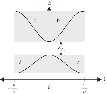
Figure 2.6
Plot of  versus
  in reduced zone scheme taken from regions a, b, c, and d in Figure 2.5
Translating the shaded regions along the k‐axis by![]() is permitted for the following reason: Revisiting the Bloch function
ψ(x) = u(x)e
ikx
of Eq. 2.5, we note that since
u(x) is periodic, we can write
ψ(x + a) = u(x)e
ikx
e
ika
, where
a
is the unit cell length. If
is permitted for the following reason: Revisiting the Bloch function
ψ(x) = u(x)e
ikx
of Eq. 2.5, we note that since
u(x) is periodic, we can write
ψ(x + a) = u(x)e
ikx
e
ika
, where
a
is the unit cell length. If ![]() then e
ika
= e
ik2nπ=1 and hence,
ψ(x + a) = ψ(x). No physical change has occurred to the description of the electron. Hence, a shift of
then e
ika
= e
ik2nπ=1 and hence,
ψ(x + a) = ψ(x). No physical change has occurred to the description of the electron. Hence, a shift of ![]() along the k‐axis is really merely a consequence of a shift in location within an infinite crystal by one unit cell of length
a
on an x‐axis. This explains the repeating patterns in Figures 2.4 and 2.5. In fact, any
k
‐value outside of the first Brillouin zone may be shifted back into the first Brillouin zone by moving it an integer number of shifts of
along the k‐axis is really merely a consequence of a shift in location within an infinite crystal by one unit cell of length
a
on an x‐axis. This explains the repeating patterns in Figures 2.4 and 2.5. In fact, any
k
‐value outside of the first Brillouin zone may be shifted back into the first Brillouin zone by moving it an integer number of shifts of ![]() . We conclude that the reduced zone scheme limiting electron wave numbers to the range
. We conclude that the reduced zone scheme limiting electron wave numbers to the range ![]() is valid.
is valid.
We now understand that the lower energy band in Figure 2.6 within shaded regions c and d shares the same k values as the upper band in regions a and b. The wave functions and therefore the energy ranges for the two bands differ, however. This occurs because a set of discrete energy bands for each given value of k corresponds to the set of discrete wave numbers Km in Equation 2.6. Figure 2.6 shows only two of many possible energy bands.
In summary, we can now view electrons moving in a periodic potential as being analogous to free electrons, but with dispersion curves having shapes shown in Figure 2.6 that differ from the free electron parabola. In Section 2.6, the treatment of these electrons will be simplified to extend our analogy to free electrons even further.
2.6 Effective Mass
We now introduce the concept of effective mass m* to allow us to quantify electron behaviour. Effective mass changes in a peculiar fashion near Brillouin zone boundaries, and generally is not the same as the free electron mass m. It is easy to understand that the effective acceleration of an electron in a crystal due to an applied electric field will depend strongly on the nature of the reflections of electron waves off crystal planes. Rather than trying to calculate the specific reflections for each electron, we instead modify the mass of the electron to account for its observed willingness to accelerate in the presence of an applied force.
We start by looking at the free electron discussed in Example 1.5, Chapter 1, with the free electron relationship
Upon taking the second derivative with respect to k, we obtain
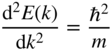
Solving for m, we obtain

Note that the electron mass is inversely proportional to the curvature of the free electron E(k) parabola shown in Figure 2.5.
If the electron is in a periodic potential, then according to the Kronig–Penney model, it will have an E versus k dependence as shown in Figure 2.6. Provided we restrict our attention to electrons that are close to the top or the bottom of an energy gap, we can approximate the dependence of E versus k to be parabolic with the general equation
where E ′ and m* are constants. Note that m* may be positive or negative. Again taking the second derivative of E with respect to k and solving for m*,we obtain
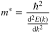
where m*, defined as the effective mass, is determined by the curvature of the specific parabola in Figure 2.6. This curvature, in turn, depends on the details of the periodic potential energy of the specific crystal in which the electron travels. If an electron exists in one of these parabolic bands, its group velocity v g as discussed in Section 1.5 is
Note that the group velocity falls to zero at the Brillouin zone boundaries where the slope of the E versus k graph is zero. This is consistent with the case of a standing wave.
In general, m* differs from free electron mass m due to the influence of the periodic potential. It is interesting to note that m* may be negative for certain values of k. This may be understood physically: if an electron that is close to the Bragg condition is accelerated slightly by an applied force, it may then move even closer to the Bragg condition, reflect more strongly off the lattice planes, and effectively accelerate in the direction opposite to the applied force.
2.7 Number of States in a Band
The curves in Figure 2.6 are misleading in that electron states in real crystals are discrete and only a finite number of states exist within each energy band. This means that the curves should be regarded as many closely spaced points that represent quantum states.
Up until now, we have assumed one‐dimensional crystals having a periodic potential energy of infinite length along the x‐axis, which is physically impossible. In order to determine the number of states in a band, we need to consider a semiconductor crystal of finite length L. We start by approximating the crystal as a potential well of length L with potential energy U = 0 inside the well.
The problem of an electron in a potential well was analysed in Section 1.8, but we will now assume infinite potential energy boundaries (see Example 2.1).
From Example 2.1 we obtain wave functions
where n is a quantum number, having wave numbers
As n increases, we will eventually reach the k value corresponding to the Brillouin zone boundary from the band model
This will occur when
and therefore ![]() where n is the number of available states in a band. Note that n is the macroscopic length of the semiconductor crystal divided by the unit cell dimension, which is simply the number of unit cells in the crystal, which we shall call N. Since electrons have an additional quantum number s (spin quantum number) that may be either
where n is the number of available states in a band. Note that n is the macroscopic length of the semiconductor crystal divided by the unit cell dimension, which is simply the number of unit cells in the crystal, which we shall call N. Since electrons have an additional quantum number s (spin quantum number) that may be either ![]() or
or ![]() , the maximum number of electrons that can occupy an energy band becomes
n
b = 2N
.
, the maximum number of electrons that can occupy an energy band becomes
n
b = 2N
.
In Section 2.10, we will introduce a three‐dimensional model of electron behaviour in a semiconductor crystal and it will be possible to show that the same result n b = 2N is also valid in a three‐dimensional crystal (see Problem 2.3).
We are now ready to determine the actual number of electrons in a band, which will allow us to understand electrical conductivity in semiconductor materials.
2.8 Band Filling
The actual number of electrons in a band is limited by the number of available states, but depends upon how many of these states are occupied. At low temperatures, the electrons will occupy the lowest allowed energy levels, and in a semiconductor such as silicon, which has 14 electrons per atom, several low‐lying energy bands will be filled. In addition, the highest occupied energy band will be full, and then the next energy band will be empty. This occurs because silicon has an even number of valence electrons per unit cell, and when there are N unit cells, there will be the correct number of electrons to fill the 2N states in the highest occupied energy band. A similar argument occurs for germanium as well as carbon (diamond), although diamond is an insulator due to its large energy gap.
Compound semiconductors such as gallium arsenide (GaAs) and other III–V semiconductors as well as CdS, and other II–VI semiconductors exhibit the same result: The total number of electrons per unit cell is even, and at very low temperatures in a semiconductor, the highest occupied band is filled and the next higher band is empty.
In many other crystalline solids, this is not the case. For example, group III elements Al, Ga, and In have an odd number of electrons per unit cell, resulting in the highest occupied band being half‐filled since the 2N states in this band will only have N electrons to fill them. These are metals. Figure 2.7 illustrates the cases we have described, showing the electron filling picture in semiconductors, insulators, and metals.
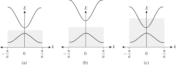
Figure 2.7 The filling of the energy bands in (a) semiconductors, (b) insulators, and (c) metals at temperatures approaching 0 K. Available electron states in the hatched regions are filled with electrons and the energy states at higher energies are empty. In band gaps there are no energy states and therefore, although the filling of available energy states is shown hatched, no electrons can exist
In Figure 2.7a, the lowest empty band is separated from the highest filled band by an energy gap E g that, in semiconductors, is typically in the range from <1 eV to between 3 and 4 eV. A completely filled energy band will not result in electrical conductivity because for each electron with a positive wave number k , there will be one having negative wave number −k . The result is a net electron wave number of zero within the band. There is no net electron momentum, and hence, no net electron flux even if an electric field is applied to the material.
Electrons may be promoted across the energy gap E g by thermal or optical energy, in which case the filled band is no longer completely full and the empty band is no longer completely empty, and now electrical conduction occurs.
Insulators (Figure 2.7b), typically have E g in the range from about 4 eV to over 6 eV. In these materials, it is difficult to promote electrons across the energy gap.
In metals, Figure 2.7c shows a partly filled energy band as the highest occupied band. The energy gap has almost no influence on electrical properties, whereas occupied and vacant electron states within this partly filled band are significant: strong electron conduction takes place in metals because empty states exist in the highest occupied band, and electrons may be promoted very easily into higher energy states within this band such that a net electron momentum is produced by a non‐zero net wave number. A very small applied electric field is enough to promote some electrons into the higher energy states that impart the net momentum to the electrons within the band and electron flow or electric current results.
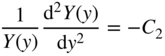
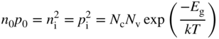
2.9 Fermi Energy and Holes
We have seen that partly filled energy bands are of particular interest since they can give rise to electric currents. In semiconductors, we have seen that a number of electrons may exist near the bottom of the lowest normally empty band due to electrons promoted across the energy gap from the highest normally filled band by thermal or optical excitation. The highest normally empty band is named the conduction band because a net electron flux or flow may be obtained in this band. The band directly below the conduction band is almost full; however, because there are empty states near the top of this band, it also exhibits conduction and is named the valence band. The electrons that occupy the valence band are valence electrons, which exist in covalent bonds in a semiconductor such as silicon or partly covalent bonds in compound semiconductors that have mixed covalent/ionic bonding character.
Figure 2.8 shows the room temperature picture of a semiconductor in thermal equilibrium. Rather than an abrupt point along the energy axis defining the boundary between regions of occupied and unoccupied electron states, there is a more gradual transition between these regions along the energy axis. We define an imaginary horizontal line at energy E f, called the Fermi energy. The Fermi energy represents an energy above which the probability of electron states being filled is under 50%, and below which the probability of electron states being filled is over 50%. We call the empty states in the valence band holes. Both valence band holes and conduction band electrons contribute to electrical conductivity.
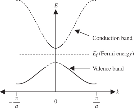
Figure 2.8 Room temperature semiconductor showing the partial filling of the conduction band and partial emptying of the valence band. Valence band holes are formed due to electrons being promoted across the energy gap. The Fermi energy lies between the bands. Solid lines represent energy states that have a significant chance of being filled
In a semiconductor, we can illustrate the valence band using Figure 2.9, which shows a simplified two‐dimensional view of silicon atoms bonded covalently. Each covalent bond requires two electrons. The electrons in each bond are not unique to a given bond and are shared between all the covalent bonds in the crystal, which means that the electron wave functions extend spatially throughout the crystal as described by Bloch functions. A valence electron can be thermally or optically excited and may leave a bond to form an electron–hole pair (EHP). The energy required for this is the band gap energy of the semiconductor. Note that there are multiple band gaps in crystalline materials as discussed in Section 2.4, but the technologically important band gap is the one lying between the valence band and the conduction band, and we will henceforth use this definition for the band gap of a given semiconductor. Once the electron leaves a covalent bond, a hole is created. Since valence electrons form spatially extended states, the hole is, similarly, shared among bonds and is able to move through the crystal. At the same time, the electron that was excited enters the conduction band and is also able to move through the crystal resulting in two independent charge carriers.
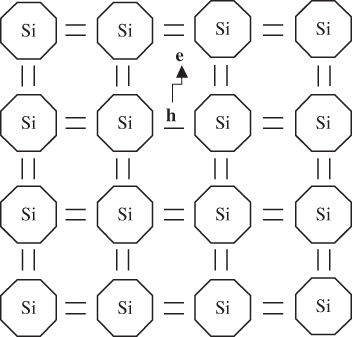
Figure 2.9 Silicon atoms have four covalent bonds as shown. Although silicon bonds are tetrahedral, they are illustrated in two dimensions for simplicity. Each bond requires two electrons, and an electron may be excited across the energy gap to result in both a hole in the valence band and an electron in the conduction band that are free to move independently of each other
In order to calculate the conductivity arising from a particular energy band, we need to know the number of electrons n per unit volume of semiconductor, and the number of holes p per unit volume of semiconductor resulting from the excitation of electrons across the energy gap E g. In the special case of a pure or intrinsic semiconductor, we can write the carrier concentrations in thermal equilibrium as n i and p i such that n i = p i.
2.10 Carrier Concentration
The determination of n and p requires us to examine the states in the conduction band that have a significant probability of being occupied by an electron, and the states in the valence band that have a significant probability of being occupied by a hole, and for each state, we need to determine the probability of occupancy to give an appropriate weighting to the state.
We will assume a constant effective mass for the electrons or holes in a given energy band. In real semiconductor materials, the relevant band states are either near the top of the valence band or near the bottom of the conduction band as illustrated in Figure 2.8. In both cases, the band shape may be approximated by a parabola, which yields a constant curvature and hence a constant effective mass as expressed in Eq. 2.18.
In contrast to effective mass, the probability of occupancy by an electron in each band state depends strongly on energy, and we cannot assume a fixed value. We use the Fermi–Dirac distribution function, which may be derived from Boltzmann statistics as follows. Consider a crystal lattice having lattice vibrations, or phonons, that transfer energy to electrons in the crystal. These electrons that occupy quantum states can also transfer energy back to the lattice, and a thermal equilibrium will be established.
Consider an electron in a crystal that may occupy lower and higher energy states ![]() and
and ![]() , respectively, and a lattice phonon that may occupy lower and higher energy states
, respectively, and a lattice phonon that may occupy lower and higher energy states ![]() and
and ![]() , respectively. Assume that this electron makes a transition from energy
, respectively. Assume that this electron makes a transition from energy ![]() to
to ![]() by accepting energy from the lattice phonon while the phonon makes a transition from
by accepting energy from the lattice phonon while the phonon makes a transition from ![]() to
to ![]() . For conservation of energy,
. For conservation of energy,
The probability of these transitions occurring can now be analysed. Let p(E
e) be the probability that the electron occupies a state having energy E
e. Let p(E
p) be the probability that the phonon occupies an energy state having energy E
p. For a system in thermal equilibrium, the probability of an electron transition from ![]() to
to ![]() is the same as the probability of a transition from
is the same as the probability of a transition from ![]() to
to ![]() , and we can write
, and we can write
because the probability that an electron makes a transition from ![]() to
to ![]() is proportional to the terms on the left‐hand side in which the phonon at
is proportional to the terms on the left‐hand side in which the phonon at ![]() must be available and the electron at
must be available and the electron at ![]() must be available. In addition, the electron state at
must be available. In addition, the electron state at ![]() must be vacant because electrons, unlike phonons, must obey the Pauli exclusion principle, which allows only one electron per quantum state. Similarly, the probability that the electron makes a transition from
must be vacant because electrons, unlike phonons, must obey the Pauli exclusion principle, which allows only one electron per quantum state. Similarly, the probability that the electron makes a transition from ![]() to
to ![]() is proportional to the terms on the right‐hand side.
is proportional to the terms on the right‐hand side.
From Boltzmann statistics (see Appendix 4) for phonons or lattice vibrations, we use the Boltzmann distribution function:
Combining Eqs. 2.21 and 2.22 we obtain
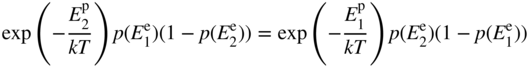
which may be written
Using Eq. 2.20, this can be expressed entirely in terms of electron energy levels as
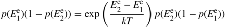
Rearranging this, we obtain
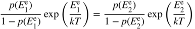
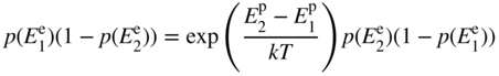
The left‐hand side of this equation is a function only of the initial electron energy level, and the right‐hand side is only a function of the final electron energy level. Since the equation must always hold and the initial and final energies may be chosen arbitrarily, we must conclude that both sides of the equation are equal to an energy‐independent quantity, which can only be a function of the remaining variable T. Let this function be f(T). Hence, using either the left‐hand side or the right‐hand side of the equation, we can write
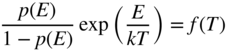
where E represents the electron energy level.
Solving for p(E), we obtain
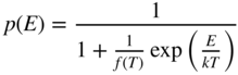
We now formally define the Fermi energy E
f to be the energy level at which ![]() and hence
and hence
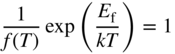
or
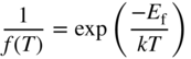
Under equilibrium conditions, the final form of the probability of occupancy at temperature T for an electron state having energy E is now obtained by substituting this into Eq. 2.24 to obtain
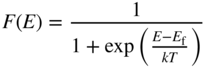
where F(E) is used in place of p(E) to indicate that this is the Fermi–Dirac distribution function. This function is graphed in Figure 2.10.
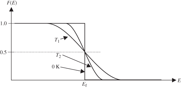
Figure 2.10
Plot of the Fermi–Dirac distribution function
 , which gives the probability of occupancy by an electron of an energy state having energy
  . The plot is shown for two temperatures
  as well as for 0 K. At absolute zero, the function becomes a step function
F(E) is 0.5 at E = E f provided T > 0 K, and at high temperatures, the transition becomes more gradual due to increased thermal activation of electrons from lower energy levels to higher energy levels. Figure 2.11 shows F(E) plotted beside a semiconductor band diagram with the energy axis in the vertical direction. The bottom of the conduction band is at E c, and the top of the valence band is at E v. At E f, there are no electron states since it is in the energy gap; however, above E c and below E v, the values of F(E) indicate the probability of electron occupancy in the bands. In the valence band, the probability for a hole to exist at any energy level is 1 − F(E).
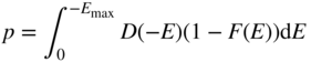
In Section 2.7, we found the total number of electron states in an energy band; however, the distribution of available energy levels in an energy band was not examined. We now require more detailed information about this distribution within the energy band. This is achieved by finding the density of states function D(E), which gives the number of available energy states per unit volume of the semiconductor over a differential energy range. It is needed in order to calculate the number of electrons or holes in an energy band. Knowing both the density of available energy states in a band and the probability of occupancy of these states in the band is essential. Once we have all this information, we can obtain the total number of electrons or holes in a band.
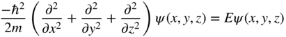
The one‐dimensional physics we have developed in Section 2.7 now needs to be extended into three dimensions. The three‐dimensional density of states function may be derived by solving Schrödinger's equation for an infinite‐walled potential box in which the wave functions must be expressed in three dimensions. In three dimensions, Schrödinger's equation is:

Firstly, consider a box of dimensions a, b, and c in three‐dimensional space in which V = 0 inside the box when 0 < x < a, 0 < y < b, 0 < z < c. Outside the box, assume that V = ∞.
Inside the box using Schrödinger's equation:
If we let ψ(x, y, z) = X(x)Y(y)Z(z), then upon substitution into Eq. 2.26 and after dividing by ψ(x, y, z), we obtain:
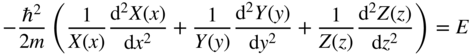
Since each term contains an independent variable, we can apply the method of separation of variables and conclude that each term is equal to a constant that is independent of x, y, and z.
Now, we have three equations
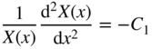
and
where
The general solution to Eq. 2.27a is
To satisfy boundary conditions such that X(x) = 0 at x = 0 and at x = a, we obtain
where
with n x a positive integer quantum number and
Note that each sinusoidal solution of X(x) comes from Eq. 2.29, which represents two travelling plane waves. This is consistent with the formation of a standing wave from two oppositely directed travelling waves.
Repeating a similar procedure for Eqs. 2.27b and 2.27c, and using Eq. 2.28, we obtain:
and

If more than one electron is put into the box at a temperature of 0 K, the available energy states will be filled such that the lowest energy states are filled first.
We now need to determine how many electrons can occupy a specific energy range in the box. It is very helpful to define a three‐dimensional space with coordinates ![]() ,
, ![]() , and
, and ![]() . In this three‐dimensional space, there are discrete points that are defined by these coordinates with integer values of n
x
, n
y
, and n
z
in what is referred to as a reciprocal space lattice, which is shown in Figure 2.12.
. In this three‐dimensional space, there are discrete points that are defined by these coordinates with integer values of n
x
, n
y
, and n
z
in what is referred to as a reciprocal space lattice, which is shown in Figure 2.12.
Figure 2.11
A semiconductor band diagram is plotted along with the Fermi–Dirac distribution function. This shows the probability of occupancy of electron states in the conduction band as well as the valence band. Hole energies increase in the negative direction along the energy axis. The hole having the lowest possible energy occurs at the top of the valence band. This occurs because by convention, the energy axis represents electron energies and not hole energies. The origin of the energy axis is located at  for convenience
From Eq. 2.30, it is seen that a spherical shell in reciprocal space represents an equal energy surface because the general form of this equation is that of a sphere in reciprocal space. The number of reciprocal lattice points that are contained inside the positive octant of a sphere having a volume corresponding to a specific energy E will be the number of states smaller than E. The number of electrons is actually twice the number of these points because electrons have an additional quantum number s for spin and ![]() . The positive octant of the sphere is illustrated in Figure 2.13.
. The positive octant of the sphere is illustrated in Figure 2.13.
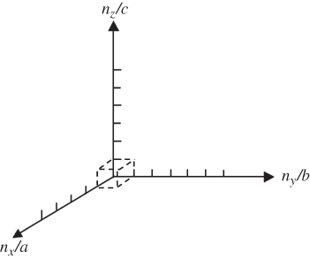
Figure 2.12
Reciprocal space lattice. A cell in this space is shown, which is the volume associated with one lattice point. The cell has dimensions  and volume
  . The axes all have the same reciprocal length units, but the relative spacing between reciprocal space lattice points along each axis depends on the relative values of
  ,
,  , and
, and 
Rearranging Eq. 2.30 where r is the sphere radius in reciprocal space, we obtain
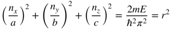
The number of reciprocal lattice points inside the sphere may be obtained from the volume of the sphere divided by the volume associated with each lattice point shown in Figure 2.12.
The volume of the sphere is
Using Eq. 2.31, we obtain
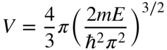
Now if the volume of the sphere is much larger than the volume associated with one lattice point then, including spin, the number of electrons having energy less than E approaches two times one‐eighth of the volume of the positive octant of the sphere divided by the volume associated with one lattice point, or:
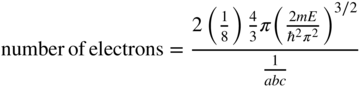
We define n(E) to be the number of electrons per unit volume of the box and therefore
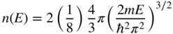
We also define D(E) to be the density of states function where
and finally, we obtain
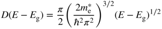
This form of the density of states function is valid for a box having V = 0 inside the box. In an energy band, however, V is a periodic function and the density of states function must be modified. This is easy to do because rather than the parabolic E versus k dispersion relation of Eq. 2.17 for free electrons in which the electron mass is m, we must use the E versus k dependence for an electron near the bottom or top of an energy band as illustrated in Figure 2.13. As discussed in Section 2.6, this dependence may be approximated as parabolic for small values of k. From Section 2.5, the relevant dispersion curve is now
where we have chosen the origin of the energy axis to coincide with the top or bottom of the relevant energy band. It is important to remember that the density of states function is based on a density of available states in reciprocal space, and that for a specific range of k‐values, the corresponding range of energies along the energy axis is determined by the slope of the E versus k graph. The slope of E versus k in a parabolic band is controlled by the effective mass.
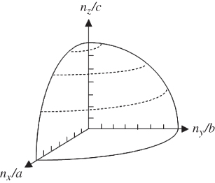
Figure 2.13 The positive octant of an sphere in reciprocal space corresponding to an equal energy surface. The number of electron states below this energy is twice the number of reciprocal lattice points inside the positive octant of the sphere
As a result, the density of states function in a conduction band is given by Eq. 2.32, provided ![]() is used in place of m, where
is used in place of m, where ![]() is the effective mass of electrons near the bottom of the conduction band. The point E = 0 should refer to the bottom of the band. We now have
is the effective mass of electrons near the bottom of the conduction band. The point E = 0 should refer to the bottom of the band. We now have
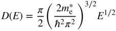
Since E v is defined as zero as in Figure 2.13 for convenience, the conduction band starts at E c = E g. D(E − E g) tells us the number of energy states available per differential range of energy within the conduction band, and we obtain
The total number of electrons per unit volume in the band is now given by
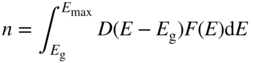
where E max is the highest energy level in the energy band that needs to be considered as higher energy levels have a negligible chance of being occupied.
From Eq. 2.25, provided E ≥ E g and E g − E f > kT, we can use the Boltzmann approximation:
Hence from Eqs. 2.33a–2.35,
The integral may be solved analytically provided the upper limit of the integral is allowed to be infinity. Using the infinite limit is allowable because the integrand becomes negligible for E > kT .
From standard integral tables and because E c = E g, we obtain
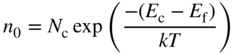
where
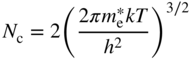
The subscript on n indicates that equilibrium conditions apply. The validity of Eqs. (2.36) is maintained regardless of the choice of the origin on the energy axis since the quantity for determining the electron concentration is the energy difference between the conduction band edge and the Fermi energy.
The same procedure may be applied to the valence band. In this case, we calculate the number of holes p in the valence band. The density of states function must be written as D(−E) since from Figure 2.11, energy E is negative in the valence band and hole energy increases as we move in the negative direction along the energy axis. We can define a hole effective mass ![]() and based on Eq. 2.32 we obtain
and based on Eq. 2.32 we obtain
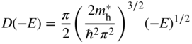
The probability of the existence of a hole is 1 − F(E), and from Eq. 2.25 if E f − E > kT, we obtain
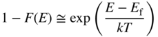
and now
In an analogous manner to that described for the conduction band, we therefore obtain
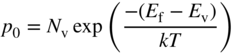
where
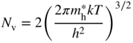
and ![]() , the hole effective mass, is a positive quantity.
, the hole effective mass, is a positive quantity.
Equation 2.37a shows that the important quantity for the calculation of hole concentration is the energy difference between the Fermi energy and the valence band edge. Again the subscript on p indicates that equilibrium conditions apply.
We can now determine the position of the Fermi level and will again set E v = 0 for convenience as illustrated in Figure 2.11. Since n i = p i for an intrinsic semiconductor, we equate Eqs. (2.36) and (2.37) and obtain
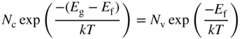
or
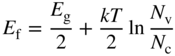
The second term on the right‐hand side of Eq. 2.38 is generally much smaller than ![]() , and we conclude that the Fermi energy lies approximately in the middle of the energy gap.
, and we conclude that the Fermi energy lies approximately in the middle of the energy gap.
From Eqs. (2.36) and (2.37), we can also write the product
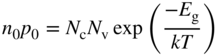
and for an intrinsic semiconductor in thermal equilibrium with n i = p i
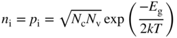
Eqs. (2.39a) and (2.39b) are very useful as they are independent of E f (see Example 2.2).
2.11 Semiconductor Materials
The relationship between carrier concentration and E g has now been established, and we can look at examples of real semiconductors. A portion of the periodic table showing elements from which many important semiconductors are made is shown in Figure 2.14, together with a list of selected semiconductors and their energy gaps. Note that there are the group IV semiconductors silicon and germanium, a number of III–V compound semiconductors having two elements, one from group III and one from group V, respectively, and a number of II–VI compound semiconductors having elements from group II and group VI, respectively.
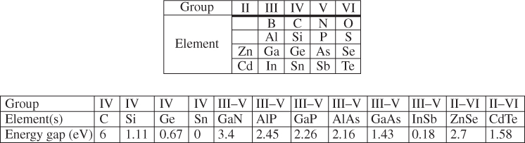
Figure 2.14 A portion of the periodic table containing some selected semiconductors composed of elements in groups II–VI
A number of interesting observations may now be made. In group IV crystals, the bonding is purely covalent. Carbon (diamond) is an insulator because it has an energy gap of 6 eV. The energy gap decreases with atomic size as we look down the group IV column from C to Si to Ge and to Sn. Actually Sn behaves like a metal. Since its energy gap is very small, it turns out that the valence band and conduction band effectively overlap when a three‐dimensional model of the crystal is considered rather than the one‐dimensional model we have discussed. This guarantees some filled states in the conduction band and empty states in the valence band regardless of temperature. Sn is properly referred to as a semimetal (its conductivity is considerably lower than metals like copper or silver). We can understand this group IV trend of decreasing energy gaps since the periodic potential of heavy elements will be weaker than that of lighter elements due to electron screening as described in Section 2.4.
As with group IV materials, the energy gaps of III–V semiconductors decrease as we go down the periodic table from AlP to GaP to AlAs to GaAs and to InSb. The energy gaps of II–VI semiconductors behave in the same manner as illustrated by ZnSe and CdTe. Again, electron screening increases for heavier elements.
If we compare the energy gaps of a set of semiconductors composed of elements from the same row of the periodic table but with increasingly ionic bonding such as Ge, GaAs, and ZnSe, another trend becomes clear: Energy gaps increase as the degree of ionic character becomes stronger. The degree of ionic bond character increases the magnitude of the periodic potential and hence the energy gap.
The carrier concentration as a function of temperature according to Eq. 2.39b is plotted for three semiconductors in Figure 2.15. Increasing energy gaps result in lower carrier concentrations at a given temperature.
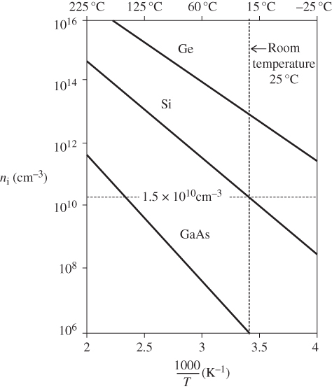
Figure 2.15
Plot of commonly accepted values of  as a function of
  for intrinsic germanium (
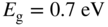 ), silicon (
 eV), and gallium arsenide (
 eV)
eV)
2.12 Semiconductor Band Diagrams
The semiconductors in Figure 2.14 crystallise in either cubic or hexagonal structures. Figure 2.16a shows the diamond structure of silicon, germanium (and carbon), which is cubic.
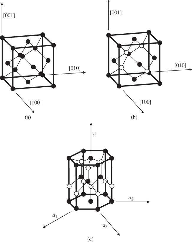
Figure 2.16
(a) The diamond unit cell of crystal structures of C, Si, and Ge. The cubic unit cell contains eight atoms. Each atom has four nearest neighbours in a tetrahedral arrangement. Within each unit cell, four atoms are arranged at the cube corners and at the face centres in a face‐centred cubic (FCC) sub‐lattice, and the other four atoms are arranged in another FCC sub‐lattice that is offset by a translation along one quarter of the body diagonal of the unit cell. (b) The zincblende unit cell contains four ‘A’ atoms (black) and four ‘B’ atoms (white). The ‘A’ atoms form an FCC sub‐lattice and the ‘B’ atoms form another FCC sub‐lattice that is offset by a translation along one quarter of the body diagonal of the unit cell. (c) The hexagonal wurtzite unit cell contains six ‘A’ atoms and six ‘B’ atoms. The ‘A’ atoms form a hexagonal close‐packed (HCP) sub‐lattice and the ‘B’ atoms form another HCP sub‐lattice that is offset by a translation along the vertical axis of the hexagonal unit cell. Each atom is tetrahedrally bonded to four nearest neighbours. A vertical axis in the unit cell is called the  ‐axis
‐axis
Figure 2.16b shows the zincblende structure of a set of III–V and II–VI semiconductors, which is also cubic. Figure 2.16c shows the hexagonal structure of some additional compound semiconductors.
These three structures have features in common. Each atom has four nearest neighbours in a tetrahedral arrangement. Some crystals exhibit distortions from the ideal 109.47° tetrahedral bond angle; however, since all the compounds have directional covalent bonding to some degree, bond angles do not vary widely. Both the cubic (111) planes and the wurtzite (1000) planes normal to the c‐axis have close‐packed hexagonal atomic arrangements.
The energy gap and effective mass values for a given semiconductor are not sufficient information for optoelectronic applications. We need to re‐examine the energy band diagrams for real materials in more detail.
The Kronig–Penney model involves several approximations. A one‐dimensional periodic potential instead of a three‐dimensional periodic potential is used. The periodic potential is simplified and does not actually replicate the atomic potentials in real semiconductor crystals. For example, silicon has a diamond crystal structure with silicon atoms as shown in Figure 2.16a. Not only are three dimensions required, but also there is more than one atom per unit cell. In addition, charges associated with individual atoms in compound semiconductors depend on the degree of ionic character in the bonding. This will affect the detailed shape of the periodic potential. The effects of electron shielding have not been accurately modelled. These and other influences from electron spin and orbital angular momentum cause energy bands in real semiconductors to differ from the idealized bands in Figure 2.8.
E versus k diagrams for various directions in a semiconductor crystal are often presented since the one‐dimensional periodic potentials vary with direction. Although three‐dimensional modelling is beyond the scope of this book, the results for cubic crystals of silicon, germanium, gallium arsenide, gallium phosphide (GaP), gallium nitride (GaN), and cadmium telluride (CdTe) as well as for wurtzite GaN are shown in Figure 2.17a–g. For cubic crystals, these figures show the band shape for an electron travelling in the [111] crystal direction on the left side and for the [100] direction on the right side. It is clear that the periodic potential experienced by an electron travelling in various directions changes: the value of a in Eq. (2.2) leading to the Bloch function (Eq. 2.5) for the [100] direction is the edge length of the cubic unit cell of the crystal. For the [111] direction, a must be modified to be the distance between the relevant atomic planes normal to the body diagonal of the unit cell. For wurtzite crystals, the two directions shown are the [0001] direction along the c‐axis and the 〈1100〉 direction along an a‐axis.
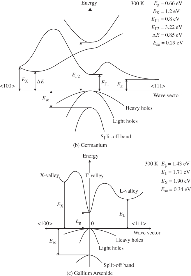
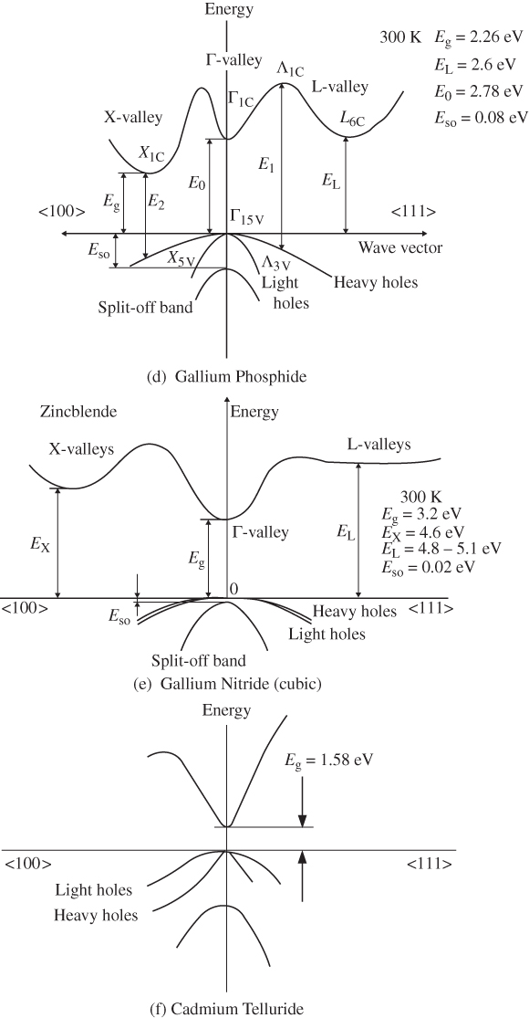
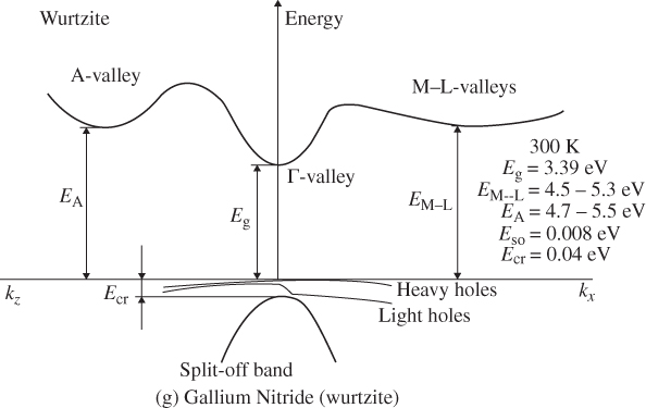
Figure 2.17
Band structures of selected semiconductors. (a) silicon, (b) germanium, (c) GaAs, (d) GaP, (e) cubic GaN, (f) CdTe, and (g) wurtzite GaN. Note that GaN is normally wurtzite. Cubic GaN is not an equilibrium phase at atmospheric pressure; however, it can be prepared at high pressure, and it is stable once grown. Note that symbols are used to describe various band features. Γ denotes the point where  . X and L denote the Brillouin zone boundaries in the 〈100〉 and 〈111〉 directions, respectively, in a cubic semiconductor. In (g)
  and
and  denote the
  and
and  directions, respectively, in a hexagonal semiconductor (see Figure 2.16c). Using the horizontal axes to depict two crystal directions saves drawing an additional figure; it is unnecessary to show the complete drawing for each
  ‐direction since the positive and negative
  ‐axes for a given
  ‐direction are symmetrical. There are also some direct energy gaps shown that are larger than the actual energy gap; the actual energy gap is the smallest gap. See Sections 2.13 and 5.2. These band diagrams are the result of both measurements and modelling results. In some cases, the energy gap values differ slightly from the values in Appendix 5.
Source: (a–d) Levinstein et al. (1996). Reprinted with permission of World Scientific; (e,g) Morkoc (2008). Copyright 2008. Reprinted with permission of Wiley‐VCH Verlag GmbH & Co. KGaA; (f) Chadov et al. (2010).
Note that there are multiple valence bands that overlap or almost overlap with each other rather than a single valence band. These are sub‐bands for holes, which are due to spin–orbit interactions that modify the band state energies for electrons in the valence band. The sub‐bands are approximately parabolic near their maxima. Because the curvatures of these sub‐bands vary, they give rise to what are referred to as heavy holes and light holes with m* as described by Eq. 2.18. There are also split‐off bands with energy maxima below the valence band edge.
2.13 Direct Gap and Indirect Gap Semiconductors
As shown in Figure 2.17, the conduction bands frequently exhibit two energy minima rather than one minimum. Each local minimum can be approximated by a parabola whose curvature will determine the effective mass of the relevant electrons.
Referring to Figure 2.17c, we can see that the band gap of GaAs is 1.43 eV where the valence band maximum and conduction band minimum coincide at k = 0. This occurs because the overall minimum of the conduction band is positioned at the same value of k as the valence band maximum, and this results in a direct gap semiconductor. As shown in Figure 2.17, GaAs, GaN, and CdTe are direct gap semiconductors. In contrast to GaAs, silicon shown in Figure 2.17a has a valence band maximum at a different value of k than the conduction band minimum. That means that the energy gap of 1.1 eV is not determined by the separation between bands at k = 0, but rather by the distance between the overall conduction band minimum and valence band maximum. This results in an indirect gap semiconductor. Another indirect gap semiconductor shown in Figure 2.17 is the III–V material GaP.
The distinction between direct and indirect gap semiconductors is of particular significance for PV and LED devices because processes involving photons occur in both cases, and photon absorption and generation properties differ considerably between these two semiconductor types.
An EHP may be created if a photon is absorbed by a semiconductor and causes an electron in the valence band to be excited into the conduction band. For example, photon absorption in silicon can occur if the photon energy matches or exceeds the band gap energy of 1.11 eV. Since silicon is an indirect gap semiconductor, however, there is a shift along the k‐axis for the electron that leaves the top of the valence band and then occupies the bottom of the conduction band. In Section 2.4, we noted that p = ℏk and therefore a shift in momentum results. The shift is considerable as seen in Figure 2.17a, and it is almost the distance from the centre of the Brillouin zone at k = 0 to the zone boundary at ![]() yielding a momentum shift of
yielding a momentum shift of
During the creation of an EHP both energy and momentum must be conserved. Energy is conserved since the photon energy ℏω satisfies the condition ℏω = E
g. Photon momentum ![]() is very small, however, and is unable to provide momentum conservation. This means that a lattice vibration, or phonon, is required to take part in the EHP generation process. The magnitudes of phonon momenta cover a wide range in crystals and a phonon with the required momentum may not be available to the EHP process. This limits the rate of EHP generation, and photons that are not absorbed continue to propagate through the silicon. This is further discussed in Section 5.2.
is very small, however, and is unable to provide momentum conservation. This means that a lattice vibration, or phonon, is required to take part in the EHP generation process. The magnitudes of phonon momenta cover a wide range in crystals and a phonon with the required momentum may not be available to the EHP process. This limits the rate of EHP generation, and photons that are not absorbed continue to propagate through the silicon. This is further discussed in Section 5.2.
If electromagnetic radiation propagates through a semiconductor, we quantify absorption using an absorption coefficient α, which determines the intensity of radiation by the exponential relationship
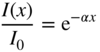
where I 0 is the initial radiation intensity and I(x) is the intensity after propagating through the semiconductor over a distance x. Efficient crystalline silicon solar cells are generally at least ≃100 µm thick for this reason due to their relatively low absorption coefficient. In contrast, GaAs (Figure 2.16c) is a direct gap semiconductor and has a much higher value of α (see Section 5.2). The thickness of GaAs required for sunlight absorption is only ≃1 µm. The value of α is an important parameter in PV semiconductors since sunlight that is not absorbed will not contribute to electric power generation. It is interesting to note that in spite of this difficulty, silicon has historically been the most important solar cell material owing to its large cost advantage over GaAs.
In LEDs, the process is reversed. EHPs recombine and give rise to photons, which are emitted as radiation. The wavelength range of this radiation may be in the infrared, the visible, or the ultraviolet parts of the electromagnetic spectrum and is dependent on the semiconductor energy gap. Silicon is a poor material for LEDs because for an EHP recombination to create a photon, one or more phonons need to be involved to achieve momentum conservation. The probability for this to occur is therefore much smaller and competing mechanisms for EHP recombination become important. These are known as non‐radiative recombination events (see Section 2.20). In contrast to silicon, GaAs can be used for high‐efficiency LEDs and was used for the first practical LED devices due to its direct gap.
2.14 Extrinsic Semiconductors
The incorporation of very small concentrations of impurities, referred to as doping, allows us to create semiconductors that are called extrinsic to distinguish them from intrinsic semiconductors, and we can control both the electron and hole concentrations over many orders of magnitude.
Consider the addition of a group V atom such as phosphorus to a silicon crystal as shown together with a band diagram in Figure 2.18. This results in an n‐type semiconductor. The phosphorus atom substitutes for a silicon atom and is called a donor; it introduces a new spatially localised energy level called the donor level E d.
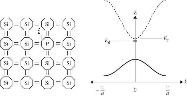
Figure 2.18
The substitution of a phosphorus atom in silicon (donor atom) results in a weakly bound extra electron occupying new energy level  that is not required to complete the covalent bonds in the crystal. It requires only a small energy
  to be excited into the conduction band, resulting in a positively charged donor ion and an extra electron in the conduction band
Because phosphorus has one more electron than silicon, this donor electron is not required for valence bonding, is only loosely bound to the phosphorus, and can easily be excited into the conduction band. The energy required for this is E c − E d and is referred to as the donor binding energy. If the donor electron has entered the conduction band, it is no longer spatially localised and the donor becomes a positively charged ion. The donor binding energy may be calculated by considering the well‐known hydrogen energy quantum states in which the ionisation energy for a hydrogen atom is given by
and the Bohr radius given by
Now, two variables in Eqs. 2.41 and 2.42 must be changed. Whereas the hydrogen electron moves in a vacuum, the donor is surrounded by semiconductor atoms, which requires us to modify the dielectric constant from the free space value ε
0 to the appropriate value for silicon by multiplying by the relative dielectric constant ε
r. In addition, the free electron mass m must be changed to the effective mass ![]() . This results in a small binding energy from Eq. 2.41 compared to the hydrogen atom and a large atomic radius from Eq. 2.42 compared to the Bohr radius. For n‐type dopants in silicon, the measured values of binding energy are approximately 0.05 eV compared to 13.6 eV for the Rydberg constant, and an atomic radius is obtained that is an order of magnitude larger than the Bohr radius of approximately 0.5 Å. Since the atomic radius is now several lattice constants in diameter, we can justify the use of the bulk silicon constants we have used in place of vacuum constants.
. This results in a small binding energy from Eq. 2.41 compared to the hydrogen atom and a large atomic radius from Eq. 2.42 compared to the Bohr radius. For n‐type dopants in silicon, the measured values of binding energy are approximately 0.05 eV compared to 13.6 eV for the Rydberg constant, and an atomic radius is obtained that is an order of magnitude larger than the Bohr radius of approximately 0.5 Å. Since the atomic radius is now several lattice constants in diameter, we can justify the use of the bulk silicon constants we have used in place of vacuum constants.
Consider now the substitution of a group III atom such as aluminium for a silicon atom as illustrated in Figure 2.19. This creates a p‐type semiconductor. The aluminium atom is called an acceptor, and it introduces a new spatially localised energy level called the acceptor level E a. Because aluminium has one fewer electron than silicon, it can accept an electron from another valence bond elsewhere in the silicon, which results in a hole in the valence band. The energy required for this is E a − E v and is referred to as the acceptor binding energy. If an electron has been accepted, the resulting hole is no longer spatially localised and the acceptor becomes a negatively charged ion. The binding energy may be estimated in a manner analogous to donor binding energies.
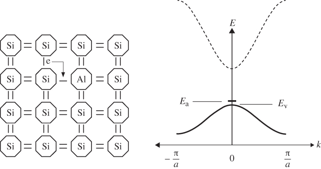
Figure 2.19
The substitution of an aluminium atom in silicon (acceptor atom) results in an incomplete valence bond for the aluminium atom. An extra electron may be transferred to fill this bond from another valence bond in the crystal. The spatially localised energy level now occupied by this extra electron at
 is slightly higher in energy than the valence band. This transfer requires only a small energy
  and results in a negatively charged acceptor ion and an extra hole in the valence band
The introduction of either donors or acceptors influences the concentrations of charge carriers, and we need to be able to calculate these concentrations. The position of the Fermi level changes when dopant atoms are added, and it is no longer true that n 0 = p 0; however, the Fermi–Dirac function F(E) still applies. A very useful expression becomes the product of electron and hole concentrations in a given semiconductor. For intrinsic material, we have calculated n i p i and we obtained Eq. 2.39b; however, Eq. (2.39a) is still valid, and we can conclude that
which is independent of E f and therefore is also applicable to extrinsic semiconductors. Here n 0 and p 0 refer to the equilibrium carrier concentrations in the doped semiconductor.
We now examine the intermediate temperature condition where the following apply:
- The ambient temperature is high enough to ionise virtually all the donors or acceptors.
- The concentration of the dopant is much higher than the intrinsic carrier concentration because the ambient temperature is not high enough to directly excite a large number of EHPs.
Under these circumstances, there are two cases. For donor doping in an n‐type semiconductor, we can conclude that
and combining Eqs. 2.43 and 2.44, we obtain

where N d is the donor concentration in donor atoms per unit volume of the semiconductor. For acceptor doping in a p‐type semiconductor, we have
and, where N a is the acceptor concentration in acceptor atoms per unit volume, we obtain

The Fermi energy levels depend upon doping and may be calculated from Eqs. (2.36) and (2.37). In the case of n‐type silicon, the Fermi level will lie closer to the conduction band. In the case of p‐type silicon, the Fermi level will lie closer to the valence band (see Figure 2.20). In Example 2.3, we calculate some specific values of the Fermi energy position.
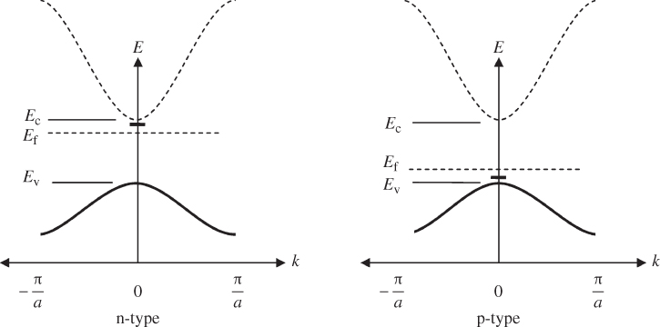
Figure 2.20 The band diagrams for n‐type silicon with a donor doping concentration of 1 × 1017 cm−3 and p‐type silicon with an acceptor doping concentration of 1 × 1017 cm−3. Note that the Fermi energy lies in the upper part of the energy gap for n‐type doping and lies in the lower part of the energy gap for p‐type doping
Consider n‐type silicon at room temperature. The mobile electrons in the n‐type silicon are called majority carriers, and the mobile holes are called minority carriers. We can also consider p‐type silicon with mobile holes called majority carriers and mobile electrons called minority carriers.
At low ambient temperatures, limited thermal energy causes only partial donor ionisation and carrier concentration drops as temperature drops. At high ambient temperatures, the intrinsic EHP concentration may be significant and may exceed the doping concentration. In this case, the semiconductor carrier concentration can be similar to that of intrinsic material. These cases are illustrated in Figure 2.21. Of particular technological importance is the intermediate temperature range since the carrier concentrations are relatively independent of temperature, and therefore, semiconductor devices can operate over wide temperature ranges without significant variation in carrier concentrations.
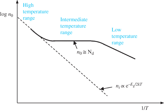
Figure 2.21
Carrier concentration as a function of temperature for an n‐type extrinsic semiconductor. In the high‐temperature range, carrier concentration is intrinsic‐like and the Fermi energy is approximately mid‐gap. In the intermediate‐temperature range, carrier concentration is controlled by the impurity concentration, virtually all the dopant atoms are ionised, and the Fermi energy is located above mid‐gap. At low temperatures, there is not enough thermal energy to completely ionise the dopant atoms, and the Fermi energy migrates to a position between
 and
and  as temperature drops. A similar diagram could be prepared for a p‐type extrinsic semiconductor
2.15 Carrier Transport in Semiconductors
The electrical conductivity of semiconductors is controlled by the concentrations of both holes and electrons and their ability to flow in a specific direction under the influence of an electric field. The flow of carriers is limited by scattering events in which carriers having a high instantaneous velocity frequently scatter off lattice vibrations (phonons), defects, and impurities, and we can denote a scattering time or characteristic mean time between scattering events for this, referred to as τ. The resulting net flow velocity or drift velocity of a stream of carriers is much lower than their instantaneous velocity. The experimental evidence for this is summarised by Ohm's law, or
which is a collision‐limited flow equation that relates the current flow to the applied electric field. To understand this, we consider Figure 2.22 showing the flow of electrons in a solid cylinder of cross‐sectional area A in the positive x direction.
Figure 2.22
Current ( ) flows along a solid semiconductor rod of cross‐sectional area
If the carrier concentration is n and each carrier carrying charge −q moves a distance dx in time dt, then the amount of charge dQ passing across a given plane in the cylinder in time dt is dQ = −nqAdx. The carrier drift velocity is given by ![]() , and we can conclude that the current is
, and we can conclude that the current is
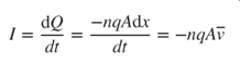
We also define the current density ![]() , and hence, we obtain Ohm's law or
, and hence, we obtain Ohm's law or
This is known as the drift current, and it requires the existence of an electric field. Note that since current is defined by convention as the flow of positive change, a negative sign is required when we consider electron drift velocity.
The application of an electric field can also be viewed using energy band diagrams. The well‐known electrostatic relationship between electric field and electric potential and energy is given by
which states that an electric field causes a gradient in electric potential V, and in addition, an electric field causes a gradient in the potential energy E of a charged particle having charge q. See Section 1.1.
We can represent the conduction and valence bands in an applied electric field by showing the situation where the conduction and valence bands are separated by the energy gap. In Figure 2.8, this occurs at k = 0. We introduce spatial dependence by using the x‐axis to show the position in the x direction of the semiconductor as in Figure 2.23. If there is no applied field, the bands are simply horizontal lines. If a constant electric field is present, the energy bands must tilt since from Eq. 2.48, there will be a constant gradient in energy and the carriers in each band will experience a force F of magnitude qε in the directions shown and will travel so as to lower their potential energies. The Fermi energy does not tilt, since the electric field does not change the thermodynamic equilibrium.
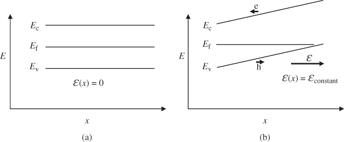
Figure 2.23 Spatial dependence of energy bands in an intrinsic semiconductor. If there is no electric field, (a) the bands are horizontal and electron and hole energies are independent of location within the semiconductor. If an electric field ε is present inside the semiconductor, the bands tilt. For an electric field pointing to the right (b), electrons in the conduction band experience a force to the left, which decreases their potential energy. Holes in the valence band experience a force to the right, which decreases their potential energy. This reversed direction for hole energies is described in Figure 2.11
We can now describe the flow of electrons. Since ![]() , we define
, we define
where μ is the carrier mobility, and we also conclude from Ohm's law that
In order to confirm the validity of Ohm's law, we can start with Newton's law of motion for an electron in an electric field
The treatment of carrier collisions requires adding the well‐known damping term ![]() where τ is the scattering time that results in a terminal velocity. This can be pictured by the example of a terminal velocity reached by a ping–pong ball falling in air. We now have
where τ is the scattering time that results in a terminal velocity. This can be pictured by the example of a terminal velocity reached by a ping–pong ball falling in air. We now have
We can demonstrate the validity of the equation in steady state where ![]() and hence
and hence
which is consistent with Ohm's law in which ![]() is proportional to
ε
, and we see that
is proportional to
ε
, and we see that
This is understandable since a longer carrier scattering time τ will increase carrier mobility and a smaller carrier effective mass will increase average carrier velocity. In addition, we can examine the case where ε = 0. Now from Eq. 2.49, we obtain
which has solution ![]() . Carrier drift velocity will decay upon removal of the electric field with characteristic time constant equal to the scattering time τ.
. Carrier drift velocity will decay upon removal of the electric field with characteristic time constant equal to the scattering time τ.
In order to consider the contribution of both electrons and holes, we write the total drift current as
where
and

Separate mobility values μ
n and μ
p are needed for electrons and holes since they flow in different bands and may have different effective masses ![]() and
and ![]() , respectively. The valence band has negative curvature, and Eq. 2.18 shows that valence band electrons have negative effective mass; however, to ensure that μ
h is a positive quantity, we define the effective mass of holes
, respectively. The valence band has negative curvature, and Eq. 2.18 shows that valence band electrons have negative effective mass; however, to ensure that μ
h is a positive quantity, we define the effective mass of holes ![]() to be a positive quantity equal in magnitude to this negative effective mass. Values of effective mass used to calculate μ
n and μ
p may differ from those in Appendix 5 due to three‐dimensional considerations (see Further Reading Section).
to be a positive quantity equal in magnitude to this negative effective mass. Values of effective mass used to calculate μ
n and μ
p may differ from those in Appendix 5 due to three‐dimensional considerations (see Further Reading Section).
Scattering time τ is determined from the combination of phonon scattering events, impurity scattering events, and defect scattering events. Since the combined scattering rate f = 1/τ is measured in scattering events per second, we can sum the scattering rates as follows:
where f phonon = 1/τ phonon , f impurity = 1/τ impurity , and f defect = 1/τ defect representing the scattering rates due to phonon scattering events, impurity scattering events, and defect scattering events, respectively. We can also express this in terms of the average scattering times for each scattering type:
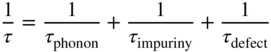
Contributions of each scattering type can be experimentally determined. For example, the phonon scattering contribution can be analysed by observing changes in mobility as temperature is changed. Increasing temperatures decrease carrier mobility.
The validity of Ohm's law has a limit. If the electric field is very large, carrier velocity magnitudes eventually saturate as shown in Figure 2.24 and will no longer be linearly proportional to the electric field. This occurs because energetic electrons transfer more energy to lattice vibrations. The magnitude of the electric field that results in saturation effects depends on the semiconductor.
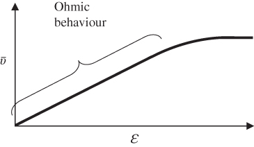
Figure 2.24 Dependence of drift velocity magnitude on electric field for a semiconductor
Mobility values for a range of semiconductors are shown in Appendix 5. These are tabulated for intrinsic materials at room temperature; however, defects and impurities as well as higher temperatures have a substantial effect on mobility values since they decrease scattering times. Both undesirable impurities and intentionally introduced dopant atoms will cause scattering times and mobility values to decrease.
2.16 Equilibrium and Non‐Equilibrium Dynamics
The carrier concentrations we have been discussing until now are equilibrium concentrations and are in thermodynamic equilibrium with the semiconductor material. In equilibrium, both EHP generation and EHP recombination occur simultaneously; however, the net EHP concentration remains constant. We can express this using rate constants defined as follows:
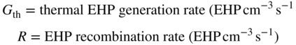
In equilibrium G th = R.
It is easy to cause a non‐equilibrium condition to exist in a semiconductor. For example, we can illuminate the semiconductor with photons whose energy exceeds the energy gap of the semiconductor. We can also cause electric current to flow through the semiconductor by attaching two or more electrodes to the semiconductor and then connecting them across a voltage source.
In an ideal direct gap semiconductor, the value of R depends on carrier concentrations. If, for example, the electron concentration n is doubled, R will double since the probability for an electron to reach a hole has doubled. If both n and p are doubled, then R will increase by a factor of 4 since the hole concentration has also doubled. We can state this mathematically as R ∝ np. We remove subscripts on carrier concentrations when non‐equilibrium conditions are present.
Consider a direct gap n‐type semiconductor in which n 0 > p 0. We shall also stipulate that δn(t) ≪ n 0, which states that the excess carrier concentration is small compared to the equilibrium majority carrier concentration (see Example 2.4).
We will now look at the time dependence of excess carrier generation. A steady optical generation rate G op is abruptly added at time t = 0. This will cause the EHP generation rate to exceed the recombination rate, and carrier concentrations will exceed the equilibrium concentrations and will become time dependent. We shall designate δn(t) and δp(t) to be the time‐dependent carrier concentrations in excess of equilibrium concentrations n 0 and p 0.
For an n‐type semiconductor in which n 0 > p 0 and in which δn(t) ≪ n 0, the net rate of increase of p is determined by the net difference between an optical generation rate and a recombination rate. From Example 2.4, the hole recombination rate is shown to be linearly proportional to excess hole concentration δp(t), and we can therefore write the simple differential equation
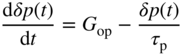
where τ p is a constant. Note that the two terms on the right‐hand side of Eq. 2.51 represent a generation rate term and a recombination rate term, respectively. The solution to this differential equation is
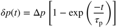
where τ p is a constant. This result is sketched in Figure 2.25.
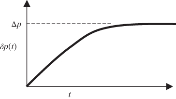
Figure 2.25
Plot of excess hole concentration as a function of time. A constant optical generation rate starts at  and continues indefinitely
After a time t > τ p, a steady‐state value of excess carrier concentration Δp exists. If Eq. 2.52 is substituted into Eq. 2.51, we obtain, for t → ∞,
The constant τ p for this process is called the carrier recombination time. Carrier recombination time should not be confused with carrier scattering time mentioned in Section 2.15. Scattering times are generally orders of magnitude shorter than recombination times.
If we know the optical generation rate and the characteristic recombination time for a semiconductor, we can calculate the steady‐state excess minority carrier concentration using Eq. 2.53a). There is also a small steady‐state change in the majority carrier concentration because Δn = Δp; however, this is neglected in low‐level injection since Δn ≪ n
0. Note that ![]() .
.
The same argument can be applied to a p‐type semiconductor, and we would obtain the increase in minority carrier concentration as
EHP recombination may also occur via processes other than direct EHP recombination events. The concept of a carrier recombination time introduced in this section is still relevant because carrier recombination times may be assigned to a variety of recombination mechanisms. Instead of calling τ n or τ p carrier recombination times, we often refer to them as carrier lifetimes, which acknowledges that direct EHP recombination may not be the dominant mechanism for carrier recombination. This is particularly true in indirect gap semiconductors such as silicon (see Section 2.20).
2.17 Carrier Diffusion and the Einstein Relation
Free carriers that are produced in a spatially localised part of a semiconductor are able to diffuse and thereby move to other parts of the material. The carrier diffusion process is functionally similar to the diffusion of atoms in solids. At sufficiently high temperatures, atomic diffusion occurs, which is described as net atomic motion from a region of higher atomic concentration to a region of lower atomic concentration. This occurs due to random movements of atoms in a concentration gradient. There is no preferred direction to the random movement of the atoms; however, provided the average concentration of atoms is not uniform, the result of random movement is for a net flux of atoms to exist, flowing from a more concentrated region to a less concentrated region. Fick's first law applies to the diffusion process for atoms as presented in introductory materials science textbooks and is also applicable to electrons.
As with atomic diffusion, the driving force for carrier diffusion is the gradient in electron concentration. For free electrons diffusing along the x‐axis, Fick's first law applies, and it can be written as
where φ n is the flux of electrons (number of electrons per unit area per second) flowing along the x‐axis due to a concentration gradient of electrons. The negative sign in Eq. 2.54 indicates that diffusion occurs in the direction of decreasing electron concentration. For holes, Fick's first law becomes
Since the flow of charged particles constitutes an electric current, we can describe diffusion currents due to holes or electrons. These are distinct from drift currents described in Section 2.15 because no electric field is involved. Eqs. 2.54 and 2.55 may be rewritten as currents:
Note that there is no negative sign in the case of electrons because electrons carry a negative charge that cancels out the negative sign in Fick's first law.
An interesting situation occurs when both diffusion and drift currents flow. An electric field is present as well as a carrier concentration gradient. The total current densities from Eqs. 2.50 and (2.56) become
and
In semiconductor diodes, both drift and diffusion occur, and it is important to become familiar with the situation where drift and diffusion currents coexist in the same part of the semiconductor.
One way to establish an electric field is to have a gradient in doping level by spatially varying the doping concentration in the semiconductor. Consider the example in Figure 2.26. The dopant concentration varies across a semiconductor sample that is in thermal equilibrium. On the left side, the semiconductor is undoped, and an acceptor dopant gradually increases in concentration from left to right. This causes the Fermi energy to occupy lower positions in the energy gap until it is close to the valence band on the right side of the sample. The Fermi energy does not tilt because it is a thermodynamic quantity and the sample is in equilibrium; however, the valence and conduction bands do tilt as shown.
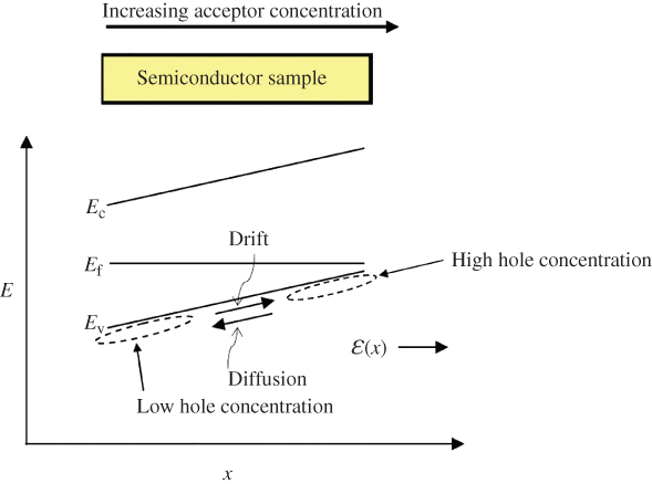
Figure 2.26 The energy bands will tilt due to a doping gradient. Acceptor concentration increases from left to right in a semiconductor sample. This causes a built‐in electric field, and the hole concentration increases from left to right. The field causes hole drift from left to right, and there is also hole diffusion from right to left due to the concentration gradient
There will now be a high concentration of holes in the valence band on the right side of the semiconductor, which decreases to a low hole concentration on the left side. Hole diffusion will therefore occur in the negative‐x direction. At the same time, the tilting of the energy bands means that an electric field is present in the sample. This is known as a built‐in electric field since it is caused by a spatial concentration variation within the semiconductor material rather than by the application of an applied voltage. The built‐in field causes a hole drift current to flow in the positive‐x direction. Since the semiconductor is in equilibrium, these two hole currents cancel out and the net hole current flow will be zero. A similar argument can be made for the electrons in the conduction band, and the net electron current will also be zero.
A useful relationship between mobility and diffusivity can now be derived. Since the net current flow illustrated in Figure 2.26 is zero in equilibrium, we can write for hole current
From Eqs. 2.48 and 2.58, we have
We now calculate p(x). Since the valence band energy E v is now a function of x, we can rewrite Eq. (2.37) as
and we obtain

which simplifies to

and a similar derivation may be applied to electrons yielding

Equation (2.60) is known as the Einstein relation. At a given temperature, this tells us that mobility and diffusivity are related by a constant factor, which is not unexpected since both quantities express the degree of ease with which carriers move in a semiconductor under a driving force.
2.18 Quasi‐Fermi Energies
If a semiconductor is influenced by incident photons or an applied electric current, the semiconductor is no longer in equilibrium. This means that we cannot use Eqs. (2.36) and (2.37) to determine carrier concentrations. In addition, Fermi energy E f is no longer a meaningful quantity since it was defined for a semiconductor in equilibrium in Section 2.9, and the Fermi–Dirac distribution function in Figure 2.10 is also based on equilibrium conditions.
For convenience, we define two new quantities, F n and F p, known as the quasi‐Fermi energy for electrons and the quasi‐Fermi energy for holes, respectively. The quantities may be used even if a semiconductor is not in equilibrium and there are excess carriers. F n and F p are defined for a semiconductor with excess carriers from the following equations:
and
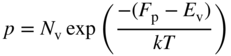
Note the similarity between Eq. (2.61) and Eqs. (2.36) and (2.37). Subscripts for n and p are absent in Eq. (2.61) because these carrier concentrations are not necessarily equilibrium values. It follows that if the semiconductor is in equilibrium, the electron and hole quasi‐Fermi energies become equal to each other and identical to the Fermi energy. The electron and hole quasi‐Fermi levels in an n‐type semiconductor will behave very differently upon excess carrier generation, as shown in Figure 2.27. This is examined in Example 2.5.
Figure 2.27
The quasi‐Fermi levels  and
and  for an n‐type semiconductor with excess carriers generated by illumination. Note the large change in
  due to illumination and note that
  is almost the same as the value of
  before illumination
The separation between F n and F p may be obtained from the product of non‐equilibrium carrier concentrations divided by the product of equilibrium carrier concentrations. This can be seen from Eqs. (2.61) and (2.43), which give us
and hence,
2.19 The Diffusion Equation
We have introduced carrier recombination as well as carrier diffusion separately; however, carriers in semiconductors routinely undergo both diffusion and recombination simultaneously.
In order to describe this, consider a long semiconductor bar or rod shown in Figure 2.28 in which excess holes are generated at x = 0 causing an excess of holes Δp to be maintained at x = 0. The excess hole concentration drops off to approach an equilibrium concentration at the other end of the long rod. The excess holes will diffuse to the right. Some of these holes recombine with electrons during this process. We can consider a slice of width dx as shown in Figure 2.28. The hole current I
p (x = a) will be higher than the hole current I
p (x = b) due to the rate of recombination of holes within volume Adx between x = a and x = b. ![]() is the hole recombination rate per unit volume. In steady state, the net hole supply and hole recombination in the slice of width dx
may be equated. Expressed mathematically, we obtain
is the hole recombination rate per unit volume. In steady state, the net hole supply and hole recombination in the slice of width dx
may be equated. Expressed mathematically, we obtain
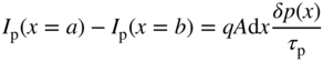
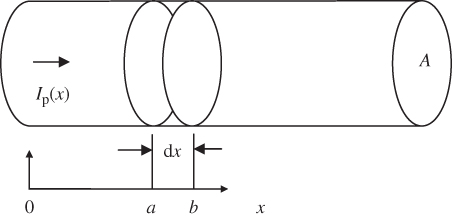
Figure 2.28
A solid semiconductor rod of cross‐sectional area  has a hole current
  flowing in the positive
  direction. Due to recombination, the hole current is dependent on
  .
.  can be analysed due to the recombination that occurs within volume
This may be rewritten as
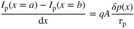
or
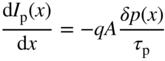
In terms of current density, we have
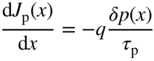
and applying the same procedure to electrons, we obtain
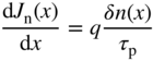
If the current is entirely due to the diffusion of carriers, we rewrite the expression for diffusion current from Eq. (2.56) for excess carriers δp(x):
Substituting this into Eq. 2.64a, we obtain
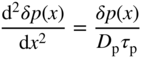
This is known as the steady‐state diffusion equation for holes, and the corresponding equation for electrons is
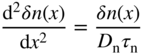
The general solution to Eq. 2.66a is
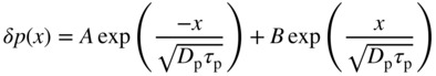
However, considering our boundary conditions, the function must decay to zero for large values of x and therefore B = 0 yielding
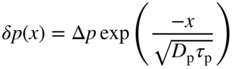
which may be written as
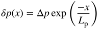
where
is known as the diffusion length. The latter determines the position on the x‐axis where carrier concentrations are reduced by a factor of e, as shown in Figure 2.29.
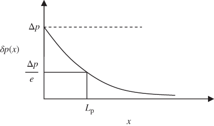
Figure 2.29
Plot of excess hole concentration in a semiconductor as a function of  in a semiconductor rod where both diffusion and recombination occur simultaneously. The decay of the concentration is characterised by a diffusion length
The hole current density at any point x may be determined by substituting Eq. 2.67b into Eq. 2.65, and we obtain
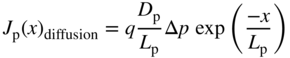
This may also be written as
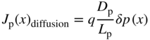
which shows that both current density and hole concentration have the same exponential form. Figure 2.30 plots current density J p(x)diffusion as a function of x. Both diffusion and recombination occur simultaneously, which lowers the diffusion current exponentially as x increases. This is reasonable since the number of holes that have not recombined drops exponentially with x and therefore L p also represents the position on the x‐axis where current density J p(x) is reduced by a factor of e.
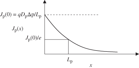
Figure 2.30
Hole current density as a function of  for a semiconductor rod with excess carriers generated at
In the case of excess electron flow, the current flow becomes
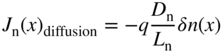
where
2.20 Traps and Carrier Lifetimes
Carrier lifetimes in many semiconductors including indirect gap silicon are really determined by trapping processes instead of ideal direct gap electron–hole recombination. Traps are impurity atoms or native point defects such as vacancies, dislocations, or grain boundaries. There are also surface traps due to the defects that inherently occur at semiconductor surfaces and interface traps that form at a boundary between two different material regions in a semiconductor device.
In all cases, traps are physical defects capable of trapping conduction band electrons and/or valence band holes and affecting carrier concentrations, carrier flow, and recombination times. This is different from a normal EHP recombination process because a specific defect is involved. After being trapped, a carrier may again be released to the band it originated from or it may subsequently recombine at the trap with a carrier of the opposite sign that also gets attracted to the same trap. This is known as trap‐assisted carrier recombination and is one of the most important phenomena that limits the performance of both direct and indirect gap semiconductors used for solar cells and LEDs. Trap‐assisted carrier recombination is often referred to as Shockley–Read–Hall (SRH) recombination.
Intentionally introduced n‐type and p‐type dopants actually are traps and are referred to as shallow traps because they are only separated from either a conduction band or a valence band by a small energy difference that may be overcome by thermal energy. This means that the trap is easy to ionise and the carrier is very likely to be released from the trap. Also, since dopants are normally ionised, they do not trap carriers of the opposite sign. For example, phosphorus in silicon is an n‐type dopant. Once it becomes a positive ion after donating an electron to the conduction band, it has a small but finite probability of recapturing a conduction band electron. Since it spends almost all its time as a positive ion, it has essentially no chance of capturing a hole, which is repelled by the positive charge, and therefore shallow traps generally do not cause trap‐assisted carrier recombination.
The traps that we must pay careful attention to are deep traps, which exist near the middle of the band gap. These traps are highly effective at promoting EHP recombination events. Since their energy levels are well separated from band edges, carriers that are trapped are not easily released. Imagine a deep trap that captures a conduction band electron and is then negatively charged. In this state, the negatively charged trap cannot readily release its trapped electron and may therefore attract a positive charge and act as an effective hole trap. Once the hole is trapped, it recombines with the trapped electron, and the trap is effectively emptied and is again available to trap another conduction band electron. In this manner, traps become a new conduit for electrons and holes to recombine. If the deep trap density is high, the average trap‐assisted recombination rate is high.
The analysis of deep trap behaviour requires that we know the probabilities of the trap being filled or empty. This may be understood in equilibrium conditions by knowing the trap energy level and comparing it to the Fermi energy level. If the trap energy level E t is above E f, then the trap is more likely to be empty than full. If E t is below E f, it is more likely to be filled. The terms ‘filled’ and ‘empty’ refer specifically to electrons because the Fermi–Dirac function describes the probability that an electron fills a specific energy level. If we wish to describe the probabilities for a trap to be occupied by holes, we must subtract these probabilities from 1.
We will simplify the treatment of traps by focusing on a very specific situation. Consider a trap at the Fermi energy and near mid‐gap in a semiconductor. Both E
t and E
f will be at approximately the middle of the energy gap. The ionisation energy of the trap for either a trapped electron or a trapped hole is approximately ![]() , as illustrated in Figure 2.31. The probability that the trap is empty or filled is 50% since it is at the Fermi energy. The captured electron may be re‐released back to the conduction band, or it may be annihilated by a hole at the trap.
, as illustrated in Figure 2.31. The probability that the trap is empty or filled is 50% since it is at the Fermi energy. The captured electron may be re‐released back to the conduction band, or it may be annihilated by a hole at the trap.
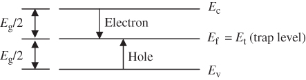
Figure 2.31 A trap level at the Fermi energy near mid‐gap
There is a simple argument for assuming that the trap is likely to exist at the Fermi level and near mid‐gap. At the surface of a semiconductor, approximately half the bonds normally formed will be broken or incomplete. This gives rise to electrons that are only held by half the atoms with which they usually are associated in the interior of a perfect crystal. These dangling bonds therefore comprise electrons that are likely to lie at approximately mid‐gap because the energy required to excite them into the conduction band is only approximately half as large as the energy E g required to remove an electron from the complete covalent bond of the relevant perfect crystal.
Now consider a large number of such dangling bonds at a semiconductor surface. Some of these dangling bonds will have lost electrons, and some of them will not. Since the Fermi level exists between the highest filled states and the lowest empty state, the Fermi level tends to fall right onto the energy level range of these traps. The Fermi energy gets pinned to this trap energy at ![]() . Figure 2.32 shows the pinning of a Fermi level due to surface traps in a p‐type semiconductor. Notice that at the semiconductor surface, the surface traps determine the position of the Fermi energy rather than the doping level. An electric field is established in the semiconductor normal to the surface and band bending occurs as shown.
. Figure 2.32 shows the pinning of a Fermi level due to surface traps in a p‐type semiconductor. Notice that at the semiconductor surface, the surface traps determine the position of the Fermi energy rather than the doping level. An electric field is established in the semiconductor normal to the surface and band bending occurs as shown.
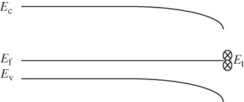
Figure 2.32
Surface traps at the surface of a p‐type semiconductor comprise electrons held in dangling bonds. The energy needed to release these electrons is approximately  . Since there are large numbers of dangling bond states, some being occupied and some not being occupied by electrons, the Fermi energy becomes pinned at this energy
If the semiconductor had been n‐type instead of p‐type, then the same reasoning would still pin the Fermi energy to mid‐gap; however, the band bending would occur in the opposite direction and the resulting electric field would point in the opposite direction, as illustrated in Figure 2.33.
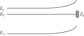
Figure 2.33 Surface traps at the surface of an n‐type semiconductor causing the Fermi level to be trapped at approximately mid‐gap. An electric field opposite in direction to that of Figure 2.32 is formed in the semiconductor
Since traps are often formed from defects other than free surfaces that also involve incomplete bonding such as a vacancy, a dislocation line, a grain boundary, or an interface between two layers, this simple picture is very useful and will be used in the context of the p–n junction to explain recombination processes in subsequent sections of this book.
There is a velocity associated with excess minority carriers at a semiconductor surface or at an interface between a semiconductor and another material. Consider diffusion current within a p‐type semiconductor having excess holes. Very close to a surface or interface,
Flux has units of particles per unit area per unit time. Since we can also define a flux as the product of concentration and velocity, we can write
where |S
n| is the surface recombination velocity of the electrons, and we evaluate δn and ![]() at the semiconductor surface. Note that if S
n = 0, we can conclude that
at the semiconductor surface. Note that if S
n = 0, we can conclude that ![]() is zero, there is no band bending, and surface states do not act as carrier traps. Conversely, if |S
n| → ∞, then δn = 0 at the surface, which implies that carriers very rapidly recombine at the surface. A similar situation exists at the surface or at an interface of an n‐type semiconductor in which holes may recombine, and we obtain
is zero, there is no band bending, and surface states do not act as carrier traps. Conversely, if |S
n| → ∞, then δn = 0 at the surface, which implies that carriers very rapidly recombine at the surface. A similar situation exists at the surface or at an interface of an n‐type semiconductor in which holes may recombine, and we obtain
In both Eqs. 2.69a and 2.69b, we assume that the excess carrier concentrations are much larger than the equilibrium minority carrier concentrations (see Example 2.6).
2.21 Alloy Semiconductors
An important variation in semiconductor compositions involves the use of partial substitutions of elements to modify composition. One example is the partial substitution of germanium in silicon that results in a range of new semiconductors of composition Si1−x Ge x , which are known as alloy semiconductors. The germanium atoms randomly occupy lattice sites normally occupied by silicon atoms, and the crystal structure of silicon is maintained. Note that Si and Ge are both in the group IV column of the periodic table and therefore have chemical similarities in terms of valence electrons and types of bonding. This means that provided no additional dopant impurities are introduced into the alloy semiconductor, alloy material with characteristics of an intrinsic semiconductor can be achieved. Of interest in semiconductor devices is the opportunity to modify the optical and electrical properties of the semiconductor. Since germanium has a smaller band gap than silicon, adding germanium decreases band gap as x increases. In addition, the average lattice constant of the new compound will increase since germanium is a larger atom than silicon. Since both germanium and silicon have the same diamond crystal structure, the available range of x is from 0 to 1 and the indirect band gaps of the alloy compositions Si1−x Ge x therefore range between 1.11 and 0.067 eV as x varies from 0 to 1, respectively.
Of more relevance to p–n junctions for solar cells and LEDs, alloy semiconductors may also be formed from compound semiconductors. For example, Ga1−x In x N is a ternary, or three‐component, alloy semiconductor in which a fraction of the gallium atoms in wurtzite GaN is replaced by indium atoms. The indium atoms randomly occupy the crystalline sites in GaN that are normally occupied by gallium atoms. Since In and Ga are both group III elements, the substitution does not act as either an acceptor or a donor. The direct band gap decreases as x increases. For x = 0, E g = 3.4 eV; and for x = 1, E g = 0.77 eV.
There are many other III–V alloy semiconductors. In Ga1−x Al x As alloys, the band gap varies from 1.43 to 2.16 eV as x goes from 0 to 1. In this system, however, the band gap is direct in the case of GaAs, but indirect in the case of AlAs. There is a transition from direct to indirect band gap at x ≅ 0.45. We can understand this transition if we consider the two conduction band minima in GaAs shown in Figure 2.17c. One minimum forms a direct energy gap with the highest energy levels in the valence band; however, the second minimum forms an indirect gap. When x ≅ 0.45, these two minima are at the same energy level. For x < 0.45, the alloy has a direct gap because the global conduction band minimum forms the direct gap. For x > 0.45, the global conduction band minimum is the minimum that forms the indirect gap.
A number of III–V alloy systems are illustrated in Figure 2.34a. An additional set of III–V nitride semiconductors is shown in Figure 2.34b, and a set of II–VI semiconductors is included in Figure 2.34c.
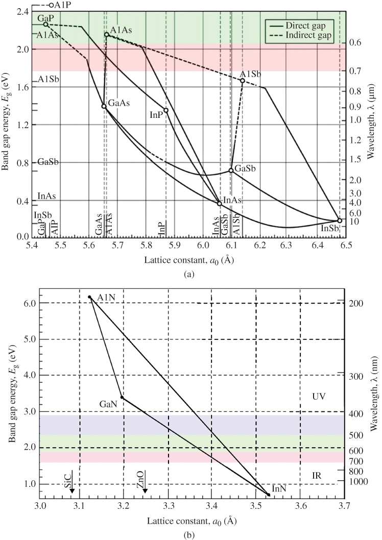
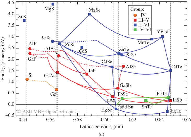
Figure 2.34 Band gap versus lattice constant for (a) phosphide, arsenide, and antimonide III–V semiconductors; (b) nitride; and other III–V semiconductors neglecting bowing (see Figure 6.20); (c) sulfide, selenide, and telluride II–VI semiconductors and phosphide, arsenide, and antimonide III–V semiconductors.
Source: (a,b) Fred Schubert (2006). Copyright 2006. Reprinted with permission of E. Fred Schubert; (c) Arizona State University (2018) with permission from Yong H. Zhang
To cover ranges of composition in the III–V alloy system, quaternary alloys may be formed such as (Al x Ga1−x ) y In1−y P. The use of ternary and quaternary semiconductor alloys in solar cells and LEDs will be discussed in Chapters 4 and 5.
2.22 Summary
- The band theory of solids permits an understanding of electrical and optical properties including electrical conductivity in metals and semiconductors, optical absorption and luminescence, and properties of junctions and surfaces of semiconductors and metals.
- The underlying form of electron wave functions in periodic potentials is found using Fourier series representations. Bloch's theorem is derived in one dimension. The existence of Brillouin zones follows directly from this, and the concept of a wave number k within the first Brillouin zone for electrons in a crystal is established.
- In the Kronig–Penney model, a periodic potential leads to energy bands and energy gaps by solving Schrödinger's equation for electrons in a periodic potential. The size of the energy gaps increases as the amplitude of the periodic potential increases. As the ionic character of the bonding in the semiconductor increases, the energy gap increases. As the size of the atoms decreases, the energy gap increases.
- The Bragg model identifies Brillouin zone boundaries as satisfying the Bragg condition for strong reflection. This condition is 2a = nλ. The reduced zone scheme, which shows only the first Brillouin zone, simplifies the representation of energy bands and energy gaps.
- The effective mass m * is used to quantify electron behaviour in response to an applied force. The effective mass depends on the band curvature. Effective mass is constant if the band shape can be approximated as parabolic.
- The number of states in a band n can be determined based on the number of unit cells N in the semiconductor sample. The result n b = 2N is obtained for a one‐dimensional, two‐dimensional, or three‐dimensional case.
- The filling of bands in semiconductors and insulators is such that the highest filled band is full and the lowest empty band is empty at low temperatures. In metals, the highest filled band is only partly filled. Semiconductors have smaller band gaps (E g = 0–4 eV) than insulators (E g > 4 eV).
- The Fermi energy E f is defined as the energy level at which an electron state has a 50% probability of occupancy at temperatures above 0 K. A hole can be created when an electron from the valence band is excited to the conduction band. The hole can move independently from the electron.
- Carrier concentration in an energy band is determined by (i) finding the probability of occupancy of the states in a band using the Fermi–Dirac distribution function F(E), and (ii) finding the density of states function D(E) for an energy band. Then the integral over the energy range of the band of the product of D(E) and F(E) will determine the number of carriers in the band. In the conduction band, the equilibrium electron concentration is n 0, and in the valence band, the equilibrium hole concentration is p 0. The product n 0 p 0 is a constant that is independent of the Fermi energy.
- A range of semiconductor materials includes group IV semiconductors, group III–V semiconductors, and group II–VI semiconductors listed in order of increasing ionic character. Band gap energies decrease for larger atoms that are lower down on the periodic table.
- Most important semiconductor crystals have lattices that are diamond, zincblende, or hexagonal structures. These structures lead to complex band diagrams. The band shapes in E versus k plots depend on crystallographic directions. In addition, there are sub‐bands in the valence band that correspond to distinct hole effective masses. Band gaps may be direct or indirect. Conduction bands generally exhibit two minima where one minimum corresponds to a direct gap transition and the other minimum corresponds to an indirect gap transition.
- Photon momentum is very small, and direct gap transitions in semiconductors are favourable for photon creation and absorption. In indirect gap transitions, the involvement of lattice vibrations or phonons is required. The absorption coefficient α is higher for direct gap semiconductors and lower for indirect gap semiconductors for photons above E g in energy. Whereas indirect gap silicon has an effective absorption depth of ≌100 µm for sunlight, the corresponding absorption depth in GaAs is only ≌1 µm.
- Pure semiconductors are known as intrinsic semiconductors. The incorporation of low levels of impurity atoms in a semiconductor leads to extrinsic semiconductors, in which the electron concentration n 0 and hole concentration p 0 are controlled by the impurity type and concentration. Donor impurities donate electrons to the conduction band in n‐type semiconductors, and acceptor impurities donate holes to the valence band in p‐type semiconductors. New shallow energy levels arise within the energy gap, which are called donor and acceptor levels. Carrier concentrations are temperature dependent; however, over a wide intermediate temperature range, carrier concentrations are relatively constant as a function of temperature. Minority carriers refer to the carriers having a low concentration in a specific semiconductor region, and majority carriers refer to the carriers having a significantly higher concentration in the same region.
- Carriers move through semiconductors in an electric field ε by a drift process, which is characterised by a drift velocity
 and mobility μ. Drift current density is given by J = σε, which is an expression of Ohm's law. The understanding of Ohm's law is based on the concept of a terminal velocity due to scattering events having a characteristic scattering time τ, which depends on impurities, defects, and temperature. At very high electric fields, drift velocity will eventually saturate.
 - Carrier concentrations are not necessarily at equilibrium levels. Photons or applied electric fields can give rise to non‐equilibrium excess carrier concentrations, which will return to equilibrium concentrations once equilibrium conditions are restored. EHP generation and recombination processes G th or G op and R define the resulting rate of generation and recombination. Under equilibrium conditions, G th = R where R ∝ np. The minority carrier lifetime time constants τ n or τ p characterise the recombination times of minority carriers.
- Carriers diffuse in semiconductors due to a concentration gradient. The diffusion coefficients D n and D p determine the diffusion currents J n and J p, respectively. The net current flow must include both drift and diffusion currents. In equilibrium, the net current is zero; however, drift and diffusion currents may be non‐zero. The Einstein relation is derived from the requirements for equilibrium conditions and allows D n and D p to be derived from μ n and μ p.
- In non‐equilibrium conditions, the Fermi energy is not defined; however, quasi‐Fermi energies F n and F p may be defined to characterise changes in carrier concentrations due to excess carrier generation.
- Combining the concepts of carrier recombination and carrier diffusion, the diffusion equation leads to the calculation of diffusion lengths
 and
and  and shows that carrier concentration decays exponentially as a function of distance from a region of excess carrier generation.
 - Traps can have a large effect on carrier lifetimes. The most important traps are deep traps that are at or near mid‐gap. A high density of such traps occurs at semiconductor interfaces and defects. This is frequently due to dangling bonds. Fermi level pinning occurs at or near mid‐gap due to dangling bonds. Surface recombination velocity is a measure of the rate of recombination at semiconductor surfaces.
- The band gap and direct/indirect nature of a semiconductor can be altered by alloying. Alloying may also change the lattice constant. Industrially important alloy semiconductors composed from group IV elements, group III–V elements, and group II–VI elements exist. Ternary and quaternary compound semiconductors are important for solar cells and LEDs.
References
- Chadov, S., Qi, X., Kübler, J. et al. (2010). Tunable multifunctional topological insulators in ternary Heusler compounds. Nature Materials 9: 541–545. doi: 10.1038/nmat2770.
- Fred Schubert, E. (2006). Light‐Emitting Diodes, 2. ISBN 978‐0‐521‐86538‐8e. Cambridge: Cambridge University Press.
- Levinstein, M., Rumyantsev, S., and Shur, M. (1996). Handbook Series on Semiconductor Parameters, vol. 1. London. ISBN 9810229348: World Scientific.
- Morkoc, H. (2008). Handbook of Nitride Semiconductors and Devices, vol. 1. Weinheim: Wiley‐VCH Verlag GmbH & Co. KGaA, ISBN 978‐3‐527‐40837‐5.
Further Reading
- Ashcroft, N.W. and Mermin, N.D. (1976). Solid State Physics. Holt, Rinehart and Winston.
- Eisberg, R. and Resnick, R. (1985). Quantum Physics of Atoms, Molecules, Solids, Nuclei and Particles, 2e. Wiley.
- Kittel, C. (2005). Introduction to Solid State Physics, 8e. Wiley.
- Neamen, D.A. (2003). Semiconductor Physics and Devices, 3e. McGraw‐Hill.
- Solymar, L. and Walsh, D. (2004). Electrical Properties of Materials, 7e. Oxford University Press.
Problems
- 2.1 Show that Eq. 2.13 may be obtained from Eqs. 2.9 to 2.12. Note that although this is basic algebra, it does require many steps to complete.
-
2.2 Show that Eq. 2.15 results from Eq. 2.14 if we define

and take b → 0 and U 0 → ∞ such that bU 0 is constant.
-
2.3 In Section 2.7, we showed that the number of states in an energy band is n
b = 2 N for a one‐dimensional semiconductor. Show that the number of states in an energy band in a three‐dimensional semiconductor is still n
b = 2 N where N is the number of unit cells in the three‐dimensional semiconductor.
Hint: Consider a semiconductor in the form of a rectangular box having N x , N y , and N z unit cells along the x‐, y‐, and z‐axes. Assume an infinite walled box with V = 0 inside the box. Use the allowed energy values for an electron in Eq. 2.30. Include spin.
- 2.4 A rectangular semiconductor crystal has dimensions 2 mm × 2 mm × 1 mm. The unit cell is cubic and has edge length of 2 Å. Find the number of states in one band of this semiconductor.
-
2.5 A rectangular silicon semiconductor bar of length 12 cm and cross‐section 1 mm × 5 mm is uniformly doped n‐type with concentration N
d = 5 × 1016 cm−3.
- Assuming that all donors are ionised, calculate the room temperature current flow if contacts are made on the two ends of the bar and 10 V is applied to the bar.
- Find the electric field in the bar for the conditions of (a).
- What fraction of the current flows in the form of hole current for the conditions of (a)?
- Find the resistivity of the silicon.
- If the silicon were replaced by gallium phosphide and the doping was still N d = 5 × 1016 cm−3, repeat (a), (b), and (c).
- If the silicon temperature was increased to 120 °C, repeat (a), (b), and (c). Assume that carrier mobility and band gap are not affected by the increase in temperature.
-
2.6 Now, instead of being uniformly doped, the bar mentioned in Problem 2.5 is doped with a linearly increasing donor doping concentration, such that the left end of the bar (LHS) is doped with a concentration of 1 × 1016 cm−3 and the right end of the bar (RHS) is doped with a concentration of 1 × 1017 cm−3.
- Determine the doping level at three points in the bar:
- at 3 cm from the LHS;
- at the midpoint;
- at 9 cm from the LHS.
- Assuming equilibrium conditions (no applied voltage), find the built‐in electric field in the bar at each of positions (i), (ii), and (iii). Hint: Find the gradient in the doping about each point.
- Find the electron drift current flowing in the bar at positions (i), (ii), and (iii).
- Explain how the bar can be in equilibrium given the existence of these electric fields and drift currents.
- Find the Fermi level relative to the top of the valence band for each of positions (i), (ii), and (iii).
- Sketch the band diagram as a function of position in equilibrium along the length of the bar showing the location of the Fermi energy.
- Determine the doping level at three points in the bar:
-
2.7 A square silicon semiconductor wafer 50 cm2 in area and 0.18 mm in thickness is uniformly doped with both acceptors (N
a = 5 × 1016 cm−3) and donors (N
d = 2 × 1016 cm−3).
- Assuming that all donors and acceptors are ionised, calculate the room temperature current flow if the silicon is contacted by narrow metal contact strips that run the full length of two opposing edges of the square silicon sheet. Ten volts is applied across the contacts.
- Repeat (a), but assume that the sheet is 100 cm2 in area instead of 50 cm2. Does the current change with area? Explain.
-
2.8 An undoped square silicon semiconductor wafer 50 cm2 in area and 0.18 mm in thickness is illuminated over one entire 50 cm2 surface and an EHP generation rate of 1021 cm−3 s−1 is achieved uniformly throughout the material.
- Determine the separation of the quasi‐Fermi levels. The carrier lifetime is 2 × 10⁻⁶ s.
- Calculate the room temperature current flow if the silicon is contacted by narrow metal contact strips that run the full length of two opposing edges of the square wafer. Ten volts is applied across the contacts under illumination conditions. The carrier lifetime is 2 × 10⁻⁶ s.
- Explain how a higher/lower recombination time would affect the answer to (b). How does the recombination time of 2 × 10⁻⁶ s compare with the transit time of the carriers, which is the time taken by the carriers to traverse the silicon sheet from one side to the other side? This silicon sheet is functioning as a photoconductive device since its conductivity depends on illumination. If the transit time is small compared to the recombination time, then gain can be obtained since more than one carrier can cross the photoconductive sheet before a recombination event takes place on average. Gains of 100 or 1000 may be obtained in practice in photoconductors. How long a recombination time would be required for a gain of 100 to be achieved? Repeat for a gain of 1000.
-
2.9 A sample of n‐type silicon is doped to achieve E
f at 0.3 eV below the conduction band edge at room temperature.
- Find the doping concentration.
- The n‐type silicon sample is in the form of a square cross‐section bar at room temperature, and it carries a current of 3 × 10⁻² A along its length. If the bar is 10 cm long and has a voltage difference of 100 V end to end, find the cross‐sectional dimensions of the bar.
- 2.10 A silicon sample is uniformly optically excited such that its quasi‐Fermi level for electrons F n is 0.419 eV above its quasi‐Fermi level for holes F p. The silicon is n‐type with donor concentration N d = 1 × 1014 cm−3. Find the optical generation rate. Assume carrier lifetime of 8 × 10⁻⁵ s.
-
2.11 An n‐type silicon wafer is 5.0 mm thick and is illuminated uniformly over its surface with blue light, which is absorbed very close to the silicon surface. Assume that a surface generation rate of holes of 3 × 1018 cm−2 s−1 is obtained over the illuminated surface and that the excess holes are generated at the silicon surface.
- Calculate the hole concentration as a function of depth assuming a hole lifetime of 2 × 10⁻⁶ s. Assume that the hole lifetime is independent of depth.
- Calculate the hole diffusion current as a function of depth.
- Calculate the recombination rate of holes as a function of depth. Hint: Note the difference in units between the given surface generation rate of holes (cm−2 s−1), which is expressed as a flux density and the recombination rate of holes near the surface (cm−3 s−1), which is expressed as a rate per unit volume. You need to think carefully about how to properly use these units.
-
2.12 Find:
- The n‐type doping concentration required to cause silicon at room temperature to have electrical conductivity 100 times higher than that of intrinsic silicon at room temperature.
- The p‐type doping concentration required to cause silicon at room temperature to have p‐type conductivity 100 times higher than that of intrinsic silicon at room temperature.
-
2.13 Intrinsic silicon is uniformly illuminated with 1014 photons cm−2 s−1 at its surface. Assume that each photon is absorbed very near the silicon surface and generates one EHP. Carrier lifetime is 6 × 10⁻⁶ s.
- Find the flux of electrons at a depth of 3 µm. Make and state any necessary assumptions.
- Find the total excess electron charge stored in the silicon, assuming that the silicon sample is very thick.
- 2.14 If the Fermi energy in an n‐type silicon semiconductor at 300 °C is 0.08 eV below the conduction band, and the donor energy level E d is 0.02 eV below the conduction band, then find the probability of ionisation of the donors.
-
2.15 For p‐type GaAs, the resistance of a rod of the material (measuring 1 mm in diameter and 40 mm in length) from end to end is measured as 4 × 10⁷ Ω at 300 K.
- Find the doping concentration.
- Find the doping concentration in an n‐type, but otherwise identical, GaAs rod having the same resistance at 300 K.
-
2.16 An intrinsic, planar, room‐temperature silicon sample is exposed to a steady flux of light at its surface. The electron concentration as a result of this is measured to be 100 times higher than n
i, the intrinsic equilibrium concentration, at a depth of 100 µm below the silicon surface. You may use the low‐level injection approximation. Carrier lifetime
τ
n = 2 × 10⁻⁶ s.
- Assuming that the light is all absorbed very near the silicon surface and that every incident photon excites one EHP, find the total photon flux.
- Find the quasi‐Fermi level for electrons relative to the Fermi level at a depth of 100 µm. Repeat for holes.
-
2.17 A famous experiment that involves both the drift and the diffusion of carriers in a semiconductor is known as the Haynes–Shockley experiment. Search for the experimental details of this experiment and answer the following:
- Make a sketch of the semiconductor sample used in the experiment as well as the location and arrangement of electrodes and the required voltages and currents as well as the connections of electrodes for the appropriate measurements to be made.
- Sketch an example of the time dependence of the output of the experiment.
- Explain how the Einstein relation can be verified using these data.
- 2.18 A silicon sample is uniformly optically excited such that its quasi‐Fermi level for electrons F n is 0.419 eV above its quasi‐Fermi level for holes F p. The silicon is n‐type with donor concentration N d = 1 × 1017 cm−3. Find the optical generation rate. Assume a carrier lifetime of 8 × 10⁻⁶ s.
- 2.19 A flash of light at time t = 0 is uniformly incident on all parts of a p‐type silicon sample with doping of 5 × 1017 cm−3. The resulting EHP concentration is 2 × 10¹⁶ EHP cm−3. Find the time‐dependent electron and hole concentrations for time t greater than zero. Assume carrier lifetime of 8 × 10⁻⁶ s.
- 2.20 Carriers are optically generated at an intrinsic silicon surface. The generation rate is 2 × 10¹⁹ EHP cm−2 s−1. Assume that all the photons are absorbed very close to the silicon surface. Find the diffusion current of electrons just below the surface, and state clearly the assumptions you used to obtain the result. Assume carrier lifetime of 8 × 10⁻⁶ s.
- 2.21 A silicon sample is doped with 6 × 10¹⁶ donors cm−3 and N a acceptors cm−3. If E f lies 0.4 eV below E f in intrinsic silicon at 300 K, find the value of N a.
- 2.22 Electric current flows down a silicon rod 1 cm in length and 0.3 mm in diameter. The silicon is n‐type with N d = 1 × 1017 cm−3. A potential difference of 10 V is applied to the rod, end to end. How many electrons drift through the rod in 60 s?
- 2.23 Find the energy difference between F n (quasi‐Fermi level for electrons under illumination) and E f (without illumination) for a silicon sample containing 1015 donors cm−3. Assume room temperature. The illumination is uniform such that 1018 EHP cm−3 s−1 are generated. Assume carrier lifetime of 8 × 10⁻⁵ s.
-
2.24
-
A p‐type silicon semiconductor is illuminated and excess carrier concentrations
δn = δp = 2 × 1016 cm−3
are generated. Find the surface recombination velocity of electrons at the semiconductor surface given the following:
- If the surface recombination velocity is zero for the same sample, calculate δn surface .
- If the surface recombination velocity is infinite for the same sample, calculate δn surface .
- Sketch a band diagram as a function of distance x from the semiconductor surface to a few diffusion lengths away from the surface. What additional carrier transport mechanism besides diffusion will be active near the silicon surface?
- Repeat (a) for a GaAs semiconductor with minority carrier lifetime τ = 100 ns.
-
A p‐type silicon semiconductor is illuminated and excess carrier concentrations
δn = δp = 2 × 1016 cm−3
are generated. Find the surface recombination velocity of electrons at the semiconductor surface given the following:
- 2.25 An n‐type silicon sample has a donor concentration of 1 × 1017 cm−3. We now illuminate this sample steadily and introduce a uniform EHP generation rate of G op = 3 × 1020 cm−3 s−1. Assume a carrier lifetime of 2.5 × 10⁻⁵ s. Find the surface recombination velocity of holes at the semiconductor surface if the surface hole concentration is 1 × 1014 cm−3 .
-
2.26 Assume a doped (extrinsic) silicon sample at room temperature.
- Calculate the separation between E c and E f for n‐type silicon having a phosphorus impurity concentration of 1 × 1015 cm−3. Find both electron and hole concentrations.
- Calculate the separation between E c and E f for p‐type silicon having an aluminium impurity concentration of 1 × 1015 cm−3. Find both electron and hole concentrations.
- Repeat (a) and (b) for germanium.
-
2.27 For semiconductor samples of silicon and germanium, assume that carrier mobility is temperature independent.
- Find the temperature at which the carrier concentration in intrinsic silicon becomes equal to 1 × 1015 cm−3.
- Repeat (a) for intrinsic germanium.
- Find the electrical conductivity σ for each of (a) and (b) at the temperatures you calculated.
- Find the electrical conductivity σ of intrinsic silicon and the electrical conductivity σ of intrinsic germanium at room temperature.
- Determine the upper temperature limits for the intermediate temperature ranges of n‐type doped silicon and n‐type doped germanium samples having doping N d = 1 × 1015 cm−3 . Use the criterion that the conductivity from thermally stimulated carriers is 10% of the conductivity due to carriers supplied by doping.
- We have assumed that carrier mobility is temperature independent. A more accurate model includes a temperature‐dependent mobility. Describe this dependence, and provide the explanation for it.