4
Photon Emission and Absorption
4.1 Introduction to Luminescence and Absorption
We have discussed the electronic aspects of a p–n junction in some detail. However, the processes by which light is absorbed or emitted are a crucial aspect of p–n junctions in solar cells and light‐emitting diodes (LEDs). The p–n junction is an ideal device to either absorb or emit photons, and these processes occur when an electron–hole pair is generated or annihilated, respectively. The p–n diode efficiently transports both electrons and holes towards a p–n junction for photon production or away from the junction for electric current generation due to photon absorption.
We will discuss the theory of luminescence in some detail, in which a photon is created by an electron–hole pair. These concepts can be readily understood in reverse to explain photon absorption as well.
Technologically important forms of luminescence may be broken down into several categories as shown in Table 4.1. Although the means by which the luminescence is excited varies; all luminescence is generated by means of accelerating charges. The portion of the electromagnetic spectrum visible to the human eye contains wavelengths from 400 to 700 nm. The evolution of the relatively narrow sensitivity range of the human eye is a complex subject, but it is intimately related to the solar spectrum, the absorbing behaviour of the terrestrial atmosphere, and the reflecting properties of terrestrial materials, green lying near the middle of the useful spectrum. Not surprisingly, the wavelength at which the human eye is most sensitive is also green.
Table 4.1 Luminescence types, applications, and typical efficiencies
| Luminescence type | Examples |
|
Blackbody radiation (light generated due to the temperature of a body) |
Sun Tungsten filament lamp (η = 5%) |
|
Photoluminescence (light emitted by a material that is stimulated by electromagnetic radiation) |
Fluorescent lamp phosphors (η = 80%) |
|
Electroluminescence (light emitted by a material that is directly electrically excited) |
Light emitting diode (η = 50%) |
Efficiency (η) is given in visible light output power as a fraction of input power.
Visible light emission is the most important wavelength range for both organic and inorganic LEDs since LEDs are heavily used for lighting and display applications. The display applications typically include red, green, and blue wavelengths in a trichromatic scheme that allows humans to perceive a wide range of colours from a set of only three primary colours.
Infrared (IR) and ultraviolet (UV) radiation must also be considered for both solar cells and LEDs. The sun includes IR and UV wavelengths, and solar cells are heavily dependent on IR absorption. Infrared LEDs are well developed and are used for remote control and sensing applications. UV‐emitting LEDs are used for industrial processing applications.
4.2 Physics of Light Emission
In order to understand the processes of light emission and light absorption in more detail, we will examine the behaviour of charges and moving charges. A stationary point charge q results in electric field lines that emanate from the charge in a radial geometry as shown in Figure 4.1. A charge moving with a uniform velocity relative to an observer gives rise to a magnetic field. Figure 4.2 shows the resulting magnetic field when the point charge moves away from an observer.

Figure 4.1
Lines of electric field  due to a point charge

Figure 4.2
Closed lines of magnetic field  due to a point charge
  moving into the page with uniform velocity
Since both electric and magnetic fields store energy, the total energy density is given by

This energy field falls off in density as we move away from the charge, but it moves along with the charge provided that the charge is either stationary or undergoing uniform motion. There is no flow of energy from the charge.
For a charge undergoing acceleration, however, energy continuously travels away from the charge. Consider the charge q in Figure 4.3. Assume that it is initially at rest in position A, then accelerates to position B, and stops there. The electric field lines now emanate from position B, but further out the lines had emanated from position A. The field lines cannot convey information about the location of the charge at speeds greater than the velocity of light c. This results in kinks in the lines of electric field, which propagate away from q with velocity c. Each time q accelerates, a new series of propagating kinks is generated. Each kink is made up of a component of ε that is transverse to the direction of expansion, which we call ε ⊥. If the velocity of the charge during its acceleration does not exceed a small fraction of c, then for large distances away from charge q,
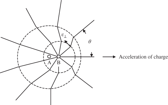
Figure 4.3 Lines of electric field emanating from an accelerating charge
Here, a is acceleration, r is the radial distance between the charge and the position where the electric field is evaluated, and θ is the angle between the direction of acceleration and the radial direction of the transverse field. The strongest transverse field occurs in directions normal to the direction of acceleration, as shown by Figure 4.3.
Similarly, a transverse magnetic field B ⊥ that points in a direction perpendicular to both acceleration and the radial direction is generated during the acceleration of the charge, as shown in Figure 4.4, and is given by
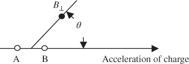
Figure 4.4
Direction of magnetic field  emanating from an accelerating charge.
  is perpendicular to both acceleration and the radial direction
The two transverse fields propagate outwards with velocity c each time q undergoes acceleration, giving rise to electromagnetic radiation. Note that ε ⊥ and B ⊥ are perpendicular to each other. The energy density of the radiation is

The Poynting vector, or energy flow per unit time (radiation intensity), is

where ![]() is a unit radial vector.
is a unit radial vector.
Maximum energy is emitted in a ring perpendicular to the direction of acceleration, and none is emitted along the direction of acceleration. To obtain the total radiated energy per unit time or power P leaving q due to its acceleration, we integrate S over a sphere surrounding q to obtain

or

Substituting for S(θ), we obtain

which can be integrated (see Problem 4.19) to obtain

4.3 Simple Harmonic Radiator
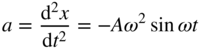
If a charge q oscillates about the origin along the x‐axis and its position is given by ![]() , then we can calculate the average power radiated away from the oscillating charge. Note that the acceleration a of the charge is given by
, then we can calculate the average power radiated away from the oscillating charge. Note that the acceleration a of the charge is given by
and using Eq. 4.1
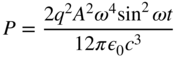
which varies with time as sin2 ωt.
To obtain average power, we integrate over one cycle to obtain

which yields

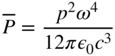
If we now consider that an equal and opposite charge is located at x = 0, then we have a dipole radiator with electric dipole moment of amplitude p = qA. This dipole may consist, for example, of an atom in which the nucleus constitutes an almost stationary charge while the electron oscillates about the nucleus. Now we may write
Radiation that does not rely on dipoles also exists. For example, a synchrotron radiation source is an example of a radiator that relies on the constant centripetal acceleration of an orbiting charge. In a synchrotron, the acceleration is in the direction of the orbit radius pointing to the centre of the orbit, and the radiation is strongest in a direction tangential to the orbit. There are also quadrupoles, magnetic dipoles, and other oscillating charge configurations that do not comprise dipoles; however, they have much lower rates of energy release, and by far, the dominant form of radiation is from dipoles.
An electron and a hole effectively behave like a dipole radiator when they recombine to create a photon. The photon is not created instantly, and many oscillations of the charges must occur before the photon is fully formed. The description of the photon as a wave packet is very relevant since the required photon energy is gradually built up as the dipole oscillates to complete the wave packet. Unless the wave packet is fully formed, no photon exists; the smallest unit of electromagnetic radiation is the photon.
Since we need to describe the positional behaviour of electrons and holes using quantum concepts, we will now proceed to introduce a simple quantum expression to incorporate in the calculation of dipole radiation.
4.4 Quantum Description
A charge q does not exhibit energy loss or radiation when in a stationary state or eigenstate of a potential energy field. This means that in a stationary state, no net acceleration of the charge occurs, in spite of its uncertainty in position and momentum within the stationary state. Experience tells us, however, that radiation may be produced when a charge moves from one stationary state to another; it will be the purpose of this section to show that radiation is produced if an oscillating dipole results from a charge moving from one stationary state to another.
Consider a charge q initially in normalised stationary state ψ n and eventually in normalised stationary state ψ n′. During the transition, a superposition state is created, which we shall call ψ s:
If
then we have normalised the superposition state. Here a and b are time‐dependent coefficients. Initially, a = 1 and b = 0 and finally, a = 0 and b = 1.
Quantum mechanics allows us to calculate the time‐dependent expected value of the position 〈r〉 (t) of a particle in a quantum state. For example, for stationary state ψ n,
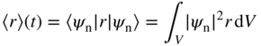
where V represents all space. For a stationary state, from Sections 1.7 and 1.8,
and hence,

This expression for 〈r〉 is therefore not a function of time, which is the fundamental idea underlying the name stationary state. A stationary state does not radiate, and there is no energy loss associated with the behaviour of an electron in such a state. Note that electrons are not truly stationary in a quantum state. It is therefore the quantum state that is described as stationary and not the electron itself. Quantum mechanics sanctions the existence of a charge that can move around in space but that does not possess a measurable acceleration. Classical physics fails to describe or predict this.
If we now calculate the expectation value of the position of q for the superposition state ψ s in the same manner we obtain, for real values of a and b

Of the four terms, the first two are stationary but the last two terms are not and therefore the time dependent part 〈r〉s(t) may be written using Eq. 4.4 as

Using the Euler formula e ix + e−ix = 2 cos x , this may be written as
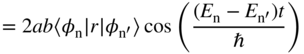
Defining ![]() and
and ![]() , we finally obtain
, we finally obtain
Here, ![]() is called the matrix element for the transition. It is seen that the expectation value of the position of the electron is oscillating with frequency
is called the matrix element for the transition. It is seen that the expectation value of the position of the electron is oscillating with frequency ![]() which is the required frequency to produce a photon having energy
which is the required frequency to produce a photon having energy ![]() . The term
. The term![]() also varies with time, but does so very slowly compared with the cosine term. This is illustrated in Figure 4.5.
also varies with time, but does so very slowly compared with the cosine term. This is illustrated in Figure 4.5.
Within matrix element ![]() , product
ab
is of order unity during most of the transition, and
, product
ab
is of order unity during most of the transition, and ![]() is the important term. For a dipole radiator,
is the important term. For a dipole radiator, ![]() can vary from zero in a dipole‐forbidden transition to a large value in a dipole radiator having a high oscillator strength.
can vary from zero in a dipole‐forbidden transition to a large value in a dipole radiator having a high oscillator strength.

Figure 4.5
A time‐dependent plot of coefficients  and
and  is consistent with the time evolution of wave functions
  and
and  . At
. At  ,
,  , and
, and  . Next, a superposition state is formed during the transition such that
  . Finally, after the transition is complete,
  and
and 
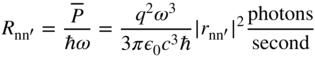
We may define a photon emission rate R nn′ of a continuously oscillating charge q. We use Eqs. 4.2 and 4.5 and E = ℏω to obtain
Note from Section 1.5 that the form of the uncertainty principle relevant to photons is ![]() . This would seem to contradict the time calculation for photon release from an oscillating dipole we have just presented. Since photon energy is defined,
ΔE
is zero, and hence, we expect time uncertainty
ΔT
for photon release to approach infinity. In fact, there is no contradiction since the time for a photon to be released from an oscillating dipole must be viewed as an expectation value. The release time for any specific photon is not known in advance, but the expected release time is known. Once again, classical physics fails to describe how certain photons emitted from an oscillating dipole can be created much more quickly or much more slowly than the expected time.
. This would seem to contradict the time calculation for photon release from an oscillating dipole we have just presented. Since photon energy is defined,
ΔE
is zero, and hence, we expect time uncertainty
ΔT
for photon release to approach infinity. In fact, there is no contradiction since the time for a photon to be released from an oscillating dipole must be viewed as an expectation value. The release time for any specific photon is not known in advance, but the expected release time is known. Once again, classical physics fails to describe how certain photons emitted from an oscillating dipole can be created much more quickly or much more slowly than the expected time.
We are now particularly interested in dipoles formed from a hole‐electron pair. A hole‐electron pair may produce one photon before it is annihilated, which leads us to examine the hole‐electron pair in more detail. Also of relevance is photon absorption, in which a hole‐electron pair is created by a photon.
4.5 The Exciton
A hole and an electron can exist as a valence band state and a conduction band state. In this model, the two particles are not localised, and they are both represented using Bloch functions in the periodic potential of the crystal lattice. If the mutual attraction between the two becomes significant, then a new description is required for their quantum states that are valid before they recombine but after they experience some mutual attraction.
The hole and electron can exist in quantum states that are actually within the energy gap. The band model in Chapter 2 does not consider this situation. Just as a hydrogen atom consists of a series of energy levels associated with the allowed quantum states of a proton and an electron, a series of energy levels associated with the quantum states of a hole and an electron also exists. This hole‐electron entity is called an exciton, and the exciton behaves in a manner that is similar to a hydrogen atom with one important exception: a hydrogen atom has the lowest energy state or ground state when its quantum number n = 1, but a exciton, which also has a ground state at n = 1, has an opportunity to be annihilated when the electron and hole eventually recombine.
The energy levels and Bohr radius for a hydrogen atom were presented in Section 2.14. For an exciton, we need to modify the electron mass m to become the reduced mass μ of the hole‐electron pair, which is given by

For direct gap semiconductors such as GaAs, this is about one order of magnitude smaller than the free electron mass m. In addition, the exciton exists inside a semiconductor rather than in a vacuum. The relative dielectric constant εr must be considered, and it is approximately 10 for typical inorganic semiconductors. Now using Eq. (2.41), we have the ground state energy for an exciton of
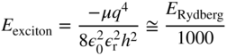
This yields a typical exciton ionisation energy or binding energy of under 0.1 eV. Using Eq. (2.42), the exciton radius in the ground state (n = 1) will be given by
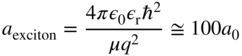
which yields an exciton radius of the order of 50 Å. Since this radius is much larger than the lattice constant of a semiconductor, we are justified in our use of the bulk semiconductor parameters for effective mass and relative dielectric constant.
Our picture is now of a hydrogen‐atom‐like entity drifting around within the semiconductor crystal and having a series of energy levels analogous to those in a hydrogen atom. Just as a hydrogen atom has energy levels ![]() where quantum number n is an integer, the exciton has similar energy levels but in a much smaller energy range, and a quantum number n is again used.
where quantum number n is an integer, the exciton has similar energy levels but in a much smaller energy range, and a quantum number n is again used.
The exciton must transfer energy to be annihilated. When an electron and a hole form an exciton, it is expected that they are initially in a high energy level with a large quantum number n. This forms a larger, less tightly bound exciton. Through thermalisation, the exciton loses energy to lattice vibrations and approaches its ground state. Its radius decreases as n approaches 1. Once the exciton is more tightly bound and n is a small integer, the hole and electron can then form an effective dipole, and radiation may be produced to account for the remaining energy and to annihilate the exciton through the process of dipole radiation. We can represent the exciton energy levels in a semiconductor as shown in Figure 4.6.
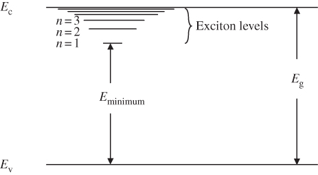
Figure 4.6
The exciton forms a series of closely spaced hydrogen‐like energy levels that extend inside the energy gap of a semiconductor. If an electron falls into the lowest energy state of the exciton corresponding to  , then the remaining energy available for a photon is
At low temperatures, the emission and absorption wavelengths of electron–hole pairs must be understood in the context of excitons in all p–n junctions. The existence of excitons, however, is generally not observable at room temperature and at higher temperatures in inorganic semiconductors because of the temperature of operation of the device. The exciton is not stable enough to form from the distributed band states, and at room temperature, kT is generally larger than the exciton binding energy. In this case, the spectral features associated with excitons will be masked, and direct gap or indirect gap band‐to‐band transitions occur. Nevertheless, photoluminescence or absorption measurements at low temperatures conveniently provided in the laboratory using liquid nitrogen (77 K) or liquid helium (4.2 K) clearly show exciton features, and excitons have become an important tool to study inorganic semiconductor behaviour. An example of the transmission as a function of photon energy of a semiconductor at low temperature due to excitons is shown in Figure 4.7.

Figure 4.7 Low‐temperature transmission as a function of photon energy for Cu2O. The absorption of photons is caused through excitons, which are excited into higher energy levels as the absorption process takes place. Cu2O is a semiconductor with a band gap of 2.17 eV.
Source: Reprinted from Kittel (1986). Copyright (1986) John Wiley and Sons, Australia
In a direct gap semiconductor dipole radiation can occur. The electron and hole in a direct gap semiconductor share the same average linear momentum and may therefore form an oscillating dipole. Electron–hole pair recombination in an indirect gap semiconductor crystal through dipole radiation is forbidden because the electron and hole have different momentum values and dipoles cannot be formed unless a phonon is involved (see Section 2.13). In an indirect gap inorganic semiconductor at room temperature, the hole–electron pair is likely to be fully annihilated through energy loss to phonons rather than through dipole radiation. The requirement of a direct gap for a band‐to‐band transition that conserves momentum is consistent with the requirements of dipole radiation.
Not all excitons are free to move around in a semiconductor. Bound excitons are often formed that associate themselves with defects in a semiconductor crystal such as vacancies and impurities. In organic semiconductors, molecular excitons form, which are very important for an understanding of optical processes that occur in organic semiconductors. This is because molecular excitons typically have high binding energies of approximately 0.4 eV. The reason for the higher binding energy is the confinement of the molecular exciton to smaller spatial dimensions and hence a smaller effective exciton radius. This keeps the hole and electron closer and increases the binding energy compared to free excitons. In contrast to the situation in inorganic semiconductors, molecular excitons are thermally stable at room temperature, and they determine emission and absorption characteristics of organic semiconductors. The molecular exciton will be discussed in Section 4.7. We will, however, first need to cover some interesting quantum physics associated with systems containing more than one electron.
4.6 Two‐Electron Atoms
Until now we have focused on dipole radiators that are composed of two charges, one positive and one negative. In Section 4.3, we introduced an oscillating dipole having one positive charge and one negative charge. In Section 4.5, we discussed the exciton in an inorganic semiconductor formed by an electron and a hole, which also therefore has a positive and a negative change. Photons can be produced as these excitons annihilate, or photons can be absorbed as they are created.
We also need to understand optical absorption and radiation from molecular systems containing two or more electrons per molecule. These electrons cooperate intimately during molecular dipole absorption and radiation events. This cooperation forms the basis of optically active organic semiconductors. Once a system has two or more identical particles (electrons), there are additional and very fundamental quantum effects that we need to consider.
The best starting point to gain further understanding is the helium atom, which has a nucleus with a charge of +2q as well as two electrons each with a charge of –q. A straightforward solution to the helium atom using Schrödinger's equation is not possible since this is a three‐body system; however, we can understand the behaviour of such a system by revisiting the Pauli exclusion principle and by including the spin states of the two electrons.
When two electrons at least partly overlap spatially with one another, their wave functions must conform to the Pauli exclusion principle; however, there is an additional requirement that must be satisfied. The two electrons must be carefully treated as indistinguishable because once they have even a small spatial overlap, there is no way to know which electron is which. We can only determine a probability density |ψ|2 = ψ * ψ for each wave function, but we cannot determine the precise location of either electron at any instant in time, and therefore, there is always a chance that the electrons exchange places. There is no way to label or otherwise identify each electron and the wave functions must therefore not be specific about the identity of each electron.
If we start with Schrödinger's equation and write it by adding up the energy terms from the two electrons, we obtain

Here ψ T (x 1 , y 1 , z 1 , x 2 , y 2 , z 2) is the wave function of the two‐electron system, V T (x 1 , y 1 , z 1 , x 2 , y 2 , z 2) is the potential energy for the two‐electron system, and E T is the total energy of the two‐electron system. The spatial coordinates of the two electrons are (x 1 , y 1 , z 1) and (x 2 , y 2 , z 2).
To simplify our treatment of the two electrons, we will start by assuming that the electrons do not interact with each other. This means that we are neglecting coulomb repulsion between the electrons. The potential energy of the total system is then simply the sum of the potential energy of each electron under the influence of the helium nucleus. Now the potential energy can be expressed as the sum of two identical potential energy functions V (x, y, z) for the two electrons, and we can write
Substituting this into Eq. 4.7, we obtain

If we look for solutions for ψ T of the form ψ T = ψ(x 1 , y 1 , z 1)ψ(x 2 , y 2 , z 2), then Eq. 4.8 becomes

Dividing Eq. 4.9 by ψ(x 1 , y 1 , z 1)ψ(x 2 , y 2 , z 2), we obtain
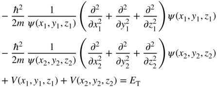
Since the first and third terms are only a function of (x 1 , y 1 , z 1) and the second and fourth terms are only a function of (x 2 , y 2 , z 2), and furthermore since the equation must be satisfied for independent choices of (x 1 , y 1 , z 1) and (x 2 , y 2 , z 2), it follows that we must independently satisfy two equations, namely
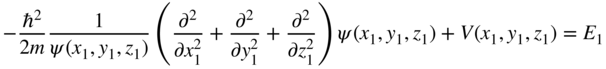
and

These are both identical one‐electron Schrödinger equations. We have used the technique of separation of variables.
We have considered only the spatial parts of the wave functions of the electrons; however, electrons also have spin. In order to include spin, the wave functions must define the spin direction of the electron.
We will write a complete wave function [ψ(x 1 , y 1 , z 1)ψ(s)] a , which is the wave function for one electron where ψ(x 1 , y 1 , z 1) describes the spatial part and the spin wave function ψ(s) describes the spin part, which can be spin up or spin down. 1 There will be four quantum numbers associated with each wave function of which the first three arise from the spatial part. A fourth quantum number, which can be +½ or −½ for the spin part, defines the direction of the spin part. Rather than writing the full set of quantum numbers for each wave function, we will use the subscript a to denote the set of four quantum numbers. For the other electron, the analogous wave function is [ψ(x 2 , y 2 , z 2)ψ(s)] b indicating that this electron has its own set of four quantum numbers denoted by subscript b.
Now the wave function of the two‐electron system including spin becomes
The probability distribution function, which describes the spatial probability density function of the two‐electron system, is |ψ T|2, which can be written as

If the electrons were distinguishable, then we would need to also consider the case where the electrons were in the opposite states, and in this case,
Now the probability density of the two‐electron system would be

Clearly Eq. 4.11b is not the same as Eq. 4.10b, because when the subscripts are switched, the form of |ψ T|2 changes. This specifically contradicts the requirement that measurable quantities such as the spatial distribution function of the two‐electron system must remain the same regardless of the interchange of the electrons.
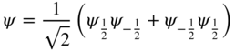
In order to resolve this difficulty, it is possible to write wave functions of the two‐electron system that are linear combinations of the two possible electron wave functions.
We write a symmetric wave function ψ S for the two‐electron system as
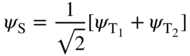
and an antisymmetric wave function ψ A for the two‐electron system as
If ψ
S is used in place of ψ
T to calculate the probability density function |ψ
S|2, the result will be independent of the choice of the subscripts. In addition, since both ![]() are valid solutions to Schrödinger's equation (Eq. 4.8) and since ψ
S is a linear combination of these solutions, it follows that ψ
S is also a valid solution. The same argument applies to ψ
A (see Problem 4.20).
are valid solutions to Schrödinger's equation (Eq. 4.8) and since ψ
S is a linear combination of these solutions, it follows that ψ
S is also a valid solution. The same argument applies to ψ
A (see Problem 4.20).
The antisymmetric wave function ψ A may be written using Eqs. 4.13, 4.10a, and 4.11a as

If, in violation of the Pauli exclusion principle, the two electrons were in the same quantum state ![]() , which includes both position and spin, then Eq. 4.14 immediately yields ψ
A = 0, which means that such a situation cannot occur. If the symmetric wave function ψ
S of Eq. 4.12 was used instead of ψ
A, the value of ψ
S would not be zero for two electrons in the same quantum state (see Problem 4.22). For this reason, a more complete statement of the Pauli exclusion principle is that the wave function of a system of two or more indistinguishable electrons must be antisymmetric.
, which includes both position and spin, then Eq. 4.14 immediately yields ψ
A = 0, which means that such a situation cannot occur. If the symmetric wave function ψ
S of Eq. 4.12 was used instead of ψ
A, the value of ψ
S would not be zero for two electrons in the same quantum state (see Problem 4.22). For this reason, a more complete statement of the Pauli exclusion principle is that the wave function of a system of two or more indistinguishable electrons must be antisymmetric.
We will now examine just the spin parts of the wave functions for each electron. We need to consider all possible spin wave functions for the two electrons. The individual electron spin wave functions must be multiplied to obtain the spin part of the wave function for the two‐electron system as indicated in Eqs. 4.10a and 4.10b or 4.11a and 4.11b, and there are four possibilities, namely ![]() or
or ![]() or
or ![]() or
or ![]() .
.
For the first two possibilities to satisfy the requirement that the spin part of the new two‐electron wave function does not depend on which electron is which, a symmetric or an antisymmetric spin function is required. In the symmetric case, we can use a linear combination of wave functions
This is a symmetric spin wave function since changing the labels does not affect the result. The total spin for this symmetric system turns out to be s = 1. There is also an antisymmetric case for which

Here, changing the sign of the labels changes the sign of the linear combination but does not change any measurable properties, and this is therefore also consistent with the requirements for a proper description of indistinguishable particles. In this antisymmetric system, the total spin turns out to be s = 0.
The final two possibilities are symmetric cases since switching the labels makes no difference. These cases therefore do not require the use of linear combinations to be consistent with indistinguishability and are simply
and
These symmetric cases both have spin s = 1.
In summary, there are four cases, three of which, given by Eqs. 4.15, 4.17, and 4.18, are symmetric spin states and have total spin s = 1, and one of which, given by Eq. 4.16, is antisymmetric and has total spin s = 0. Note that total spin is not always simply the sum of the individual spins of the two electrons, but must take into account the addition rules for quantum spin vectors (see Further Reading). The three symmetric cases are appropriately called triplet states, and the one antisymmetric case is called a singlet state. Table 4.2 lists the four possible states.
Table 4.2 Possible spin states for a two electron system
| State | Probability (%) | Total spin | Spin arrangement | Spin symmetry | Spatial symmetry | Spatial attributes | Dipole‐allowed transition to/from singlet ground state |
| Singlet | 25 | 0 |
|
Antisymmetric | Symmetric | Electrons close to each other | Yes |
| Triplet | 75 | 1 |
|
Symmetric | Antisymmetric | Electrons far apart | No |
|
or |
|||||||
|
|
In order to obtain an antisymmetric wave function, from Eq. 4.16, either the spin part or the spatial part of the wave function may be antisymmetric. If the spin part is antisymmetric, which is a singlet state, then the Pauli exclusion restriction on the spatial part of the wave function may be lifted. The two electrons may occupy the same spatial wave function, and they may have a high probability of being close to each other.
If the spin part is symmetric, this is a triplet state and the spatial part of the wave function must be antisymmetric. The spatial density function of the antisymmetric wave function causes the two electrons to have a higher probability of existing further apart because they are in distinct spatial wave functions.
If we now introduce the coulomb repulsion between the electrons, it becomes evident that if the spin state is a singlet state, the repulsion will be higher because the electrons spend more time close to each other. If the spin state is a triplet state, the repulsion is weaker because the electrons spend more time further apart (see Figure 4.8).
Now let us return to the helium atom as an example of this. Assume that one helium electron is in the ground state of helium, which is the 1s state, and the second helium electron is in an excited state. This corresponds to an excited helium atom, and we need to understand this configuration because radiation always involves excited states.
The two helium electrons can be in a triplet state or in a singlet state. Strong dipole radiation is observed from the singlet state only, and the triplet states do not radiate. We can understand the lack of radiation from the triplet states by examining spin. The total spin of a triplet state is s = 1. The ground state of helium, however, has no net spin because if the two electrons are in the same n = 1 energy level, the spins must be in opposing directions to satisfy the Pauli exclusion principle, and there is no net spin. The ground state of helium is therefore a singlet state. There can be no triplet states in the ground state of the helium atom (see Problem 4.21).
There is a net magnetic moment generated by an electron due to its spin. This fundamental quantity of magnetism due to the spin of an electron is the Bohr magneton. See Section 1.11. If the two helium electrons are in a triplet state, there is a net magnetic moment, which can be expressed in terms of the Bohr magneton since the total spin s = 1. This means that a magnetic moment exists in the excited triplet state of helium. Photons have no charge and hence no magnetic moment. Because of this, a dipole transition from an excited triplet state to the ground singlet state is forbidden. The triplet state has a magnetic moment but the singlet state does not, and the net magnetic moment cannot be conserved. In contrast to this, the dipole transition from an excited singlet state to the ground singlet state is allowed and strong dipole radiation is observed.
The triplet states of helium are slightly lower in energy than the singlet states because the electrons repel each other less. The excited state electron is therefore more strongly bound to the nucleus. Singlet states are slightly higher in energy because the electrons repel each other more and the excited state electron is therefore less bound. The observed radiation is consistent with the energy difference between the higher energy singlet state and the ground singlet state. As expected, there is no observed radiation from the triplet excited state and the ground singlet state. The energy levels of singlet and triplet states are shown in Figure 4.9.
Figure 4.8 A depiction of the symmetric and antisymmetric wave functions and spatial density functions of a two‐electron system. (a) Singlet state with electrons closer to each other on average. (b) Triplet state with electrons further apart on average

Figure 4.9 Energy levels associated with the ground singlet state and both excited singlet and triplet states of a two electron atom. The excited singlet state has the higher energy since the electrons are closer together on average which is less stable than the excited triplet state with electrons further apart on average
We have used helium atoms to illustrate the behaviour of a two‐electron system; however, we now need to apply our understanding of these results to molecular electrons, which are important for organic light‐emitting and absorbing materials. Molecules are the basis for organic electronic materials, and molecules always contain two or more electrons in a molecular system.
4.7 Molecular Excitons
In inorganic semiconductors, electrons and holes exist as distributed wave functions, which prevent the formation of stable excitons at room temperature. In contrast to this, holes and electrons are localised within a given molecule in organic semiconductors, and the molecular exciton is thereby both stabilised and bound within a molecule of the organic semiconductor. In organic semiconductors, which are composed of molecules, excitons are clearly evident at room temperature and also at higher operational device temperatures.
An exciton in an organic semiconductor is an excited state of the molecule. A molecule contains a series of electron energy levels associated with a series of molecular orbitals that are complicated to calculate directly from Schrödinger's equation due to the complex shapes of molecules. These molecular orbitals may be occupied or unoccupied. When a molecule absorbs a quantum of energy that corresponds to a transition from one molecular orbital to another higher energy molecular orbital, the resulting electronic excited state of the molecule is a molecular exciton comprising an electron and a hole within the molecule. An electron is said to be found in the lowest unoccupied molecular orbital (LUMO) and a hole in the highest occupied molecular orbital (HOMO), and since they are both contained within the same molecule, the electron‐hole state is said to be bound. A bound exciton results, which is spatially localised to a given molecule in an organic semiconductor. Organic molecule energy levels are discussed in more detail in Chapter 7.
These molecular excitons can be classified as in the case of excited states of the helium atom, and either singlet or triplet excited states in molecules are possible. The results from Section 4.6 are relevant to these molecular excitons, and the same concepts involving electron spin, the Pauli exclusion principle, and indistinguishability are relevant because the molecule contains two or more electrons.
If a molecule in its unexcited state absorbs a photon of light, it may be excited forming an exciton in a singlet state with spin s = 0. These excited molecules typically have characteristic lifetimes on the order of nanoseconds, after which the excitation energy may be released in the form of a photon and the molecule undergoes fluorescence by a dipole‐allowed process returning to its ground state.
It is also possible for the molecule to be excited to form an exciton by electrical means rather than by the absorption of a photon. This will be described in detail in Chapter 7. Under electrical excitation, the exciton may be in a singlet or a triplet state since electrical excitation, unlike photon absorption, does not require the total spin change to be zero. There is a 75% probability of a triplet exciton and a 25% probability of a singlet exciton, as described in Table 4.2. The probability of fluorescence is therefore limited under electrical excitation to 25% because the decay of triplet excitons is not dipole‐allowed.
Another process may take place, however. Triplet excitons have a spin state with s = 1, and these spin states can frequently be coupled with the orbital angular momentum of molecular electrons, which influences the effective magnetic moment of a molecular exciton. The restriction on dipole radiation can be partly removed by this coupling, and light emission over relatively long characteristic radiation lifetimes is observed in specific molecules. These longer lifetimes from triplet states are generally on the order of milliseconds, and the process is called phosphorescence, in contrast with the shorter lifetime fluorescence from singlet states. Since excited triplet states have slightly lower energy levels than excited singlet states, triplet phosphorescence has a longer wavelength than singlet fluorescence in a given molecule.
In addition, there are other ways that a molecular exciton can lose energy. There are three possible energy loss processes that involve energy transfer from one molecule to another molecule. One important process is known as Förster resonance energy transfer. Here a molecular exciton in one molecule is established, but a neighbouring molecule is not initially excited. The excited molecule will establish an oscillating dipole moment as its exciton starts to decay in energy as a superposition state. The radiation field from this dipole is experienced by the neighbouring molecule as an oscillating field and a superposition state in the neighbouring molecule is also established. The originally excited molecule loses energy through this resonance energy transfer process to the neighbouring molecule, and finally, energy is conserved after the initial excitation energy is transferred to the neighbouring molecule without the formation of a photon. This is not the same process as photon generation and absorption since a complete photon is never created; however, only dipole‐allowed transitions from excited singlet states can participate in Förster resonance energy transfer.
Förster energy transfer depends strongly on the intermolecular spacing, and the rate of energy transfer falls off as ![]() where R is the distance between the two molecules. A simplified picture of this can be obtained using the result for the electric field of a static dipole. This field falls off as
where R is the distance between the two molecules. A simplified picture of this can be obtained using the result for the electric field of a static dipole. This field falls off as ![]() . Since the energy density in a field is proportional to the square of the field strength, it follows that the energy available to the neighbouring molecule falls of as
. Since the energy density in a field is proportional to the square of the field strength, it follows that the energy available to the neighbouring molecule falls of as ![]() . This then determines the rate of energy transfer.
. This then determines the rate of energy transfer.
Dexter electron transfer is a second energy transfer mechanism in which an excited electron state transfers from one molecule (the donor molecule) to a second molecule (the acceptor molecule). This requires a wave function overlap between the donor and acceptor, which can only occur at extremely short distances typically of the order 10–20 Å. Triplet excitons are forbidden to use the Forster resonance energy transfer process but may undergo the Dexter process which does not rely on dipole interaction.
The Dexter process involves the transfer of the electron and hole from molecule to molecule. The donor's excited state may be exchanged in a single step or in two separate charge exchange steps. The driving force is the decrease in system energy due to the transfer. This implies that the donor molecule and acceptor molecule are different molecules. This will be discussed in Chapter 7 in the context of organic LEDs. The Dexter energy transfer rate is proportional to e−αR where R is the intermolecular spacing. The exponential form is due to the exponential decrease in the wave function density function with distance.
Finally, a third process is radiative energy transfer. In this case, a photon emitted by the host is absorbed by the guest molecule. The photon may be formed by dipole radiation from the host molecule and absorbed by the converse process of dipole absorption in the guest molecule (see Section 4.4).
4.8 Band‐to‐Band Transitions
In inorganic semiconductors, the recombination between an electron and a hole occurs to yield a photon, or conversely, the absorption of a photon yields a hole–electron pair. The electron is in the conduction band and the hole is in the valence band. It is very useful to analyse these processes in the context of band theory from Chapter 2.
Consider the direct‐gap semiconductor having approximately parabolic conduction and valence bands near the bottom and top of these bands, respectively, as in Figure 4.10. Parabolic bands were introduced in Section 2.6. Two possible transition energies, E 1 and E 2, are shown, which produce two photons having two different wavelengths. Due to the very small momentum of a photon, the recombination of an electron and a hole occurs almost vertically in this diagram to satisfy conservation of momentum. The x‐axis represents the wave number k, which is proportional to momentum (see Section 2.13).
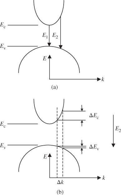
Figure 4.10
(a) Parabolic conduction and valence bands in a direct‐gap semiconductor showing two possible transitions. (b) Two ranges of energies  in the valence band and
  in the conduction band determine the photon emission rate in a small energy range about a specific transition energy. Note that the two broken vertical lines in (b) show that the range of transition energies at
  is the sum of
  and
and 
Conduction band electrons have energy
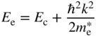
and for holes, we have

In order to determine the emission spectrum of a direct‐gap semiconductor, we need to find the probability of a recombination taking place as a function of energy E. This transition probability depends on an appropriate density of states function multiplied by probability functions that describe whether or not the states are occupied.
We will first determine the appropriate density of states function. Any transition in Figure 4.10 takes place at a fixed value of reciprocal space where k is constant. The same set of points located in reciprocal space or k‐space gives rise to states both in the valence band and in the conduction band. In the Kronig–Penny model presented in Chapter 2, a given position on the k‐axis intersects all the energy bands including the valence and conduction bands. There is therefore a state in the conduction band corresponding to a state in the valence band at a specific value of k.
Therefore in order to determine the photon emission rate over a specific range of photon energies we need to find the appropriate density of states function for a transition between a group of states in the conduction band and the corresponding group of states in the valence band. This means we need to determine the number of states in reciprocal space or k‐space that give rise to the corresponding set of transition energies that can occur over a small radiation energy range ΔE centred at some transition energy in Figure 4.10. For example, the appropriate number of states can be found at E 2 in Figure 4.10b by considering a small range of k‐states Δk that correspond to small differential energy ranges ΔE c and ΔE v and then finding the total number of band states that fall within the range ΔE. The emission energy from these states will be centred at E 2 and will have an emission energy range ΔE = ΔE c + ΔE v producing a portion of the observed emission spectrum. The density of transitions is determined by the density of states in the joint dispersion relation, which will now be introduced.
The available energy for any transition is given by
and upon substitution we can obtain the joint dispersion relation, which adds the dispersion relations from both the valence and conduction bands. We can express this transition energy E and determine the joint dispersion relation from Figure 4.10a as

where

Note that a range of k‐states Δk will result in an energy range ΔE = ΔE c + ΔE v in the joint dispersion relation because the joint dispersion relation provides the sum of the relevant ranges of energy in the two bands as required. The smallest possible value of transition energy E in the joint dispersion relation occurs at k = 0 where E = E g from Eq. 4.19, which is consistent with Figure 4.10. If we can determine the density of states in the joint dispersion relation, we will therefore have the density of possible photon emission transitions available in a certain range of energies.
The density of states function for an energy band was derived in Section 2.10. As originally derived, the form of the density of states function was valid for a box having V = 0 inside the box. In an energy band, however, the density of states function was modified. We replaced the free electron mass with the reduced mass relevant to the specific energy band, and we replaced m in Eq. (2.32) by m * to obtain Eq. (2.33a). This is valid because rather than the parabolic E versus k dispersion relation for free electrons in which the electron mass is m, we used the parabolic E versus k dispersion relation for an electron in an energy band as illustrated in Figure 2.8, which may be approximated as parabolic for small values of k with the appropriate effective mass. The slope of the E versus k dispersion relation is controlled by the effective mass, and this slope determines the density of states along the energy axis for a given density of states along the k‐axis. We can now use the same method to determine the density of states in the joint dispersion relation of Eq. 4.19 by substituting the reduced mass μ into Eq. (2.32). Recognising that the density of states function must be zero for E < E g we obtain
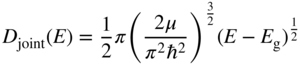
This is known as the joint density of states function valid for E ≥ E g.
To determine the probability of occupancy of states in the bands, we use Fermi–Dirac statistics, introduced in Chapter 2. The Boltzmann approximation for the probability of occupancy of carriers in a conduction band was previously obtained in Eq. (2.35) as
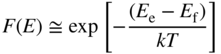
and for a valence band, the probability of a hole is given by
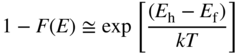
Since a transition requires both an electron in the conduction band and a hole in the valence band, the probability of a transition will be proportional to

Including the density of states function, we conclude that the probability p(E) of an electron–hole pair recombination applicable to an LED is proportional to the product of the joint density of states function and the function F(E)[1 − F(E)], which yields
Now using Eqs. 4.20 4.21 4.22, we obtain the photon emission rate R(E) as
The result is shown graphically in Figure 4.11.

Figure 4.11
Photon emission rate as a function of energy for a direct‐gap transition of an LED. Note that at low energies, the emission drops off due to the decrease in the density of states term  and at high energies, the emission drops off due to the Boltzmann term
The result expressed by Eq. 4.23 is important for direct‐gap semiconductors but differs fundamentally from the recombination rate R ∝ np previously presented in Section 2.16. This is because in Section 2.16 we assumed that carriers scattered and did not maintain a specific value of k for recombination, which is particularly relevant in an indirect gap semiconductor such as silicon. The recombination events in a semiconductor such as silicon are more likely to be non‐radiative than radiative and phonon interactions are possible. It is most likely that traps determine recombination processes and the consideration of specific values of k used to derive Eq. 4.23 is not relevant.
If we differentiate Eq. 4.23 with respect to E and set ![]() the maximum is found to occur at
the maximum is found to occur at ![]() . From this, we can evaluate the full width at half maximum to be 1.8 kT (see Problem 4.18). This will be further discussed in Chapter 6 in the context of LEDs.
. From this, we can evaluate the full width at half maximum to be 1.8 kT (see Problem 4.18). This will be further discussed in Chapter 6 in the context of LEDs.
For a solar cell, the absorption coefficient α provides the rate of absorption of photons which is the converse of the rate of emission R (see Section 2.13). We consider the valence band to be fully occupied by electrons and the conduction band to be empty. In this case, the absorption rate depends on the joint density of states function only and is independent of Fermi–Dirac statistics. Using Eq. 4.20 we obtain
The absorption edge for a direct‐gap semiconductor is illustrated in Figure 4.12.
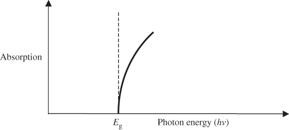
Figure 4.12 Absorption edge for direct‐gap semiconductor
This absorption edge is only valid for direct‐gap semiconductors and only when parabolic band‐shapes are valid. If hν > E g, this will not be the case and measured absorption coefficients will differ from this theory.
In an indirect‐gap semiconductor, the absorption α increases more gradually with photon energy hν until a direct‐gap transition can occur. This is discussed in more detail in Chapter 5 in the context of solar cells.
4.9 Photometric Units
The most important applications of LEDs – to be described in Chapter 6 – and organic light‐emitting diodes (OLEDs) – to be described in Chapter 7 – are for visible illumination and displays. This requires the use of units to measure the brightness and colour of light output. The power in watts and wavelengths of emission are often not adequate descriptors of light emission. The human visual system has a variety of attributes that have given rise to more appropriate units and ways of measuring light output. This human visual system includes the eye, the optic nerve, and the brain, which interpret light in a unique way. Watts, for example, are considered radiometric units, and this section introduces photometric units and relates them to radiometric units.
Luminous intensity is a photometric quantity that represents the perceived brightness of an optical source by the human eye. The unit of luminous intensity is the candela (cd). One candela is the luminous intensity of a source that emits 1/683 W of light at 555 nm into a solid angle of 1 sr. The candle was the inspiration for this unit, and a candle does produce a luminous intensity of approximately 1 cd.
Luminous flux is another photometric unit that represents the light power of a source. The unit of luminous flux is the lumen (lm). A candle that produces a luminous intensity of 1 cd produces 4π lm of light power. If the source is spherically symmetrical, then since there are 4π sr in a sphere, a luminous flux of 1 lm is emitted per steradian.
A third quantity, luminance, refers to the luminous intensity of a source divided by an area through which the source light is being emitted; it has units of cd m−2. In the case of an LED die (LED semiconductor chip) light source, the luminance depends on the size of the die. The smaller the die that can achieve a specified luminous intensity, the higher the luminance of this die.
The advantage of these units is that they directly relate to perceived brightnesses, whereas radiation measured in watts may be visible or invisible, depending on the emission spectrum. Photometric units of luminous intensity, luminous flux, and luminance take into account the relative sensitivity of the human vision system to the specific light spectrum associated with a given light source.
The eye sensitivity function is well known for the average human eye. Figure 4.13 shows the perceived brightness for the human visual system of a light source that emits a constant optical power that is independent of wavelength. The left scale has a maximum of 1 and is referenced to the peak of the human eye response at 555 nm. The right scale is in units of luminous efficacy (lm W−1), which reaches a maximum of 683 lm W−1 at 555 nm. Using Figure 4.13, luminous intensity can now be determined for other wavelengths of light.
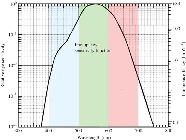
Figure 4.13 The eye sensitivity function. The left scale is referenced to the peak of the human eye response at 555 nm. The right scale is in units of luminous efficacy. International Commission on Illumination (Commission Internationale de l'Eclairage, or CIE), 1931
An important measure of the overall efficiency of a light source can be obtained using luminous efficacy from Figure 4.13. A hypothetical monochromatic electroluminescent light source emitting at 555 nm that consumes 1 W of electrical power and produces 683 lm has an electrical‐to‐optical conversion efficiency of 100%. A hypothetical monochromatic light source emitting at 410 nm that consumes 1 W of electrical power and produces approximately 5 lm also has a conversion efficiency of 100%. The luminous flux of a blue LED or a red LED that consumes 1 W of electric power may be lower than for a green LED; however, this does not necessarily mean that they are less efficient.
Luminous efficiency values for a number of light sources may be described in units of lm W−1, or light power divided by electrical input power. Table 4.3 adds the luminous efficiency values relevant to Table 4.1. Luminous efficiency can never exceed luminous efficacy for a light source having a given spectrum.
Table 4.3 Luminous efficiency values (in lm ![]() ) for a variety of light emitters
) for a variety of light emitters
|
Blackbody radiation (light generated due to the temperature of a body) |
Sun Tungsten filament lamp: η ≅ 5% or 15–20 lm W−1 |
|
Photoluminescence (light emitted by a material that is stimulated by electromagnetic radiation) |
Fluorescent lamp phosphors (η ≅ 80%) The fluorescent lamp achieves 50–80 lm W−1 and this includes the generation efficiency of UV radiation in a gas discharge |
|
Electroluminescence (light emitted by a material that is directly electrically excited) |
Light emitting diode (η ≅ 20–50%). For a 20% efficient LED this translates into the following approximate values: |
| Red LED at 625 nm 40 lm W−1 | |
| Green LED at 530 nm 120 lm W−1 | |
| Blue LED at 470 nm 12 lm W−1 |
The perceived colour of a light source is determined by its spectrum. The human visual system and the brain create our perception of colour. For example, we often perceive a mixture of red and green light as yellow even though none of the photons arriving at our eyes is yellow. For a LED, both the peak and the full width at half maximum (FWHM) of the emission spectrum determine the colour. More complex spectra due to phosphor‐converted LEDs introduced in Chapter 6 can produce perceived colours including white from more than one spectral emission peak.
The human eye contains light receptors on the retina that are sensitive in fairly broad bands centred at the red, the green, and the blue parts of the visible spectrum. Colour is determined by the relative stimulation of these receptors. For example, a light source consisting of a combination of red and green light excites the red and green receptors, as does a pure yellow light source, and we therefore perceive both light sources as yellow in colour.
Since the colours we observe are perceptions of the human visual system, a colour space has been developed and formalised that allows all the colours we recognise to be represented on a two‐dimensional graph called the colour space chromaticity diagram shown in Figure 4.14. The diagram was created by the International Commission on Illumination (Commission Internationale de l'Éclairage, or CIE) in 1931, and is therefore often referred to as the CIE diagram. CIE x and y colour coordinates are shown that can be used to specify the colour point of any light source. The outer boundary of this colour space represents monochromatic light having single wavelengths. Monochromatic light sources are considered fully saturated colours. As we move to the centre of the diagram to approach white, the light source becomes increasingly less monochromatic and less saturated. Hence, a source having a spectrum of a finite spectral width will be situated some distance inside the boundary of the colour space.

Figure 4.14 Colour space chromaticity diagram showing colours perceptible to the human eye. Numbers on the boundaries are wavelengths in nanometres. Colour saturation or purity is maximum at the boundaries, and it decreases towards the centre of the diagram, eventually becoming white. International Commission on Illumination (Commission Internationale de l'Eclairage, or CIE), 1931
If two light sources emit light at two distinct wavelengths anywhere on the CIE diagram and these light sources are combined into a single light beam, the human eye will interpret the colour of the light beam as existing on a straight line connecting the locations of the two sources on the CIE diagram. The position on the straight line of this new colour will depend on the relative radiation power from each of the two light sources (see Problem 4.23).
If three light sources emit light at three distinct wavelengths that are anywhere on the CIE diagram and these light sources are combined into a single light beam, the human eye will interpret the colour of the light beam as existing within a triangular region of the CIE diagram having vertices at each of the three sources. The position within the triangle of this new colour will depend on the relative radiation power from each of the three light sources. This ability to produce a large number of colours of light from only three light sources forms the basis for trichromatic illumination. Lamps and displays routinely take advantage of this principle. It is clear that the biggest triangle will be available if highly saturated red, green, and blue light sources are selected to define the vertices of the colour triangle. This colour triangle is often referred to as a colour space that is enabled by a specific set of three light emitters.
4.10 Summary
- Luminescence is created by accelerating charges, and examples of luminescence include blackbody radiation, photoluminescence, and electroluminescence.
- Accelerating charges emit energy through the Poynting vector, which carries electric and magnetic field energy. The total power radiated from an accelerating charge is found by integrating the radiated power over a sphere and is found to be proportional to the square of the acceleration.
- The simplest mode of charge acceleration is the oscillating dipole radiator in which a charge oscillates sinusoidally. The average power radiated by the dipole is calculated by performing a time average of the instantaneous power.
- Stationary quantum states do not radiate, whereas superposition states may radiate through dipole radiation. The expected value of the amplitude of the oscillation of the charge is determined by 〈ϕ n|r|ϕ n′〉, which may be calculated. If 〈ϕ n|r|ϕ n′〉 = 0, then radiation will not occur and the transition is forbidden.
- The exciton is formed by a hole and an electron that form a hydrogen‐like entity. Excitons in semiconductors give rise to absorption or emission lines that are observable at low temperatures. These lines exist inside the energy gap of the semiconductor. Excitons may either be free to travel through the semiconductor or they might be bound to a defect.
- The two‐electron atom involves the consideration of indistinguishable electrons. The wave functions for the two‐electron atom describe either symmetric or antisymmetric states. The resulting states are known as singlet states in which the electrons are relatively close to each other; dipole radiation is associated with singlet states and not triplet states.
- The molecular exciton comprises an electron and a hole that exist within one molecule. The exciton is bound within the molecule. The molecular exciton can be understood based on the two‐electron atom and a singlet or a triplet exciton can be achieved. Singlet molecular excitons result in a fast emission process (fluorescence). Triplet excitons are normally forbidden to radiate, but may undergo spin-orbit coupling to slowly emit photons (phosphorescence).
- Band‐to‐band transitions in a direct‐gap semiconductor produce a range of wavelengths depending on the position in the band. The distribution of electrons and holes in a band as a function of momentum may be determined by the density of states in the bands and the probabilities of occupancy of these states in the bands allowing the radiation spectrum of such a transition to be determined. In addition, the absorption spectrum in a direct‐gap semiconductor can be determined.
- The human eye perceives visible light in conjunction with the human brain, and a set of photometric units has been developed that allows our perception of brightness and colour to be quantified. Units of interest include luminance, luminous intensity, luminous flux and colour coordinates (x,y) in a two‐dimensional colour space.
References
- Kittel, C. (1986). Introduction to Solid State Physics, 6e. Australia: John Wiley and Sons. ISBN: 0‐471‐87474‐4.
Further Reading
- Ashcroft, N.W. and Mermin, N.D. (1976). Solid State Physics. Holt, Rinehart and Winston.
- Eisberg, R. and Resnick, R. (1985). Quantum Physics of Atoms, Molecules, Solids, Nuclei and Particles, 2e. Wiley.
- Griffiths, D. (2004). Introduction to Quantum Mechanics, 2e. Prentice Hall. ISBN: 0‐13‐111892‐7.
- Kittel, C. (2005). Introduction to Solid State Physics, 8e. Wiley.
- Schubert, E.F. (2006). Light Emitting Diodes, 2e. Cambridge University Press.
Problems
-
4.1 Consider an electron that oscillates in a dipole radiator and produces a radiation power of 1 × 10⁻¹² W. Find the amplitude of the oscillation of the electron if the radiation is at the following wavelengths:
- 470 nm (blue)
- 530 nm (green)
- 630 nm (red).
-
4.2 Find the time required to produce one photon from the radiator of Problem 4.1 if the radiation has wavelengths:
- 470 nm
- 530 nm
- 630 nm.
-
4.3 Find the number of photons per second required to produce an optical power of 1 W if the radiation has wavelengths:
- 470 nm
- 530 nm
- 630 nm.
-
4.4 Find the number of photons per second required to produce a luminous flux of 1 lm if the radiation has wavelengths:
- 470 nm
- 530 nm
- 630 nm.
-
4.5 Determine the luminous efficacy and the colour coordinates of light sources that emit at a single wavelength of:
- 470 nm
- 530 nm
- 630 nm.
- 4.6 Find the electric field ε ⊥ generated a distance of 100 nm from an electron that accelerates at 10 000 m s−2. Plot your result as a function of the angle between the acceleration vector and the line joining the electron to the point at which the electric field is measured. Repeat for the magnetic field B ⊥. Find the magnitude using appropriate units and the direction of the Poynting vector for the resulting travelling wave.
- 4.7 Find the total average power radiated from the charge of Problem 4.6.
-
4.8 Find the total average power radiated from an electron that oscillates at:
- A frequency of 1014 Hz with amplitude of oscillation of 0.2 nm.
- A frequency of 1015 Hz with amplitude of oscillation of 0.2 nm.
- A frequency of 1015 Hz with amplitude of oscillation of 0.5 nm.
- In what part of the electromagnetic spectrum will the radiation be for (a) and (b)? Find the wavelength in free space for the radiation of (a) and (b).
- 4.9 For each of (a), (b), and (c) in Problem 4.8, find the approximate expected length of time needed to produce one photon. What is the photon energy? What is the photon emission rate in photons per second? How many oscillations of the electron are required to produce one photon for each case?
- 4.10 Find the energy of an exciton that is formed from an electron and a hole in gallium arsenide using the appropriate effective masses and relative dielectric constant. Repeat for gallium nitride and cadmium sulfide.
- 4.11 Find the radius of an exciton in its ground state for each of the semiconductors in Problem 4.10.
- 4.12 Using a computer, plot the photon emission rate R(E) as a function of energy for a band‐to‐band recombination event in a direct‐gap semiconductor at room temperature. Cover an energy range that extends 10kT below and 10 kT above the band gap. Assume a band gap of 2 eV.
- 4.13 Silicon, being an indirect‐gap semiconductor, is very inefficient as an emission source from band‐to‐band radiation. Nevertheless, if highly purified and extremely low defect density silicon is prepared, then carrier lifetimes can become long enough for radiative recombination to compete effectively with non‐radiative emission. Search for information on this topic and prepare a short (2–3 pages) report on the state of the art on this topic. Some aspects of this topic will touch on LEDs, which are covered in Chapter 5. Keywords to consider: radiative emission in silicon; the silicon LED.
-
4.14 The colour space defined by three light emitters to form a trichromatic system in television is an important specification that contributes to the quality of the display. Find the colour coordinates of red, green, and blue emitters that are commercially accepted standards for television in both North America and in Europe, and plot these on a CIE diagram. Show the correct name for each standard. Show the triangular trichromatic colour space on the CIE diagram for each standard and comment on the limitation of this space in terms of all possible colours that the human visual system can interpret. Compare your answers to the answer to Problem 4.5. Comment on television colour coordinate standards and give possible reasons for them to be limited in colour gamut if you consider the eye sensitivity function.
Keywords to consider: CIE diagram; RGB colour coordinates; television colour gamut standards.
-
4.15 The colour coordinates of displays for portable electronics such as laptop computers generally provide smaller colour spaces than for television. Battery power is a critical limitation on the light sources used for the display and maximum display brightness is desired. Explain why a reduction in colour space is helpful with reference to the eye sensitivity function and the CIE diagram. See if you can obtain the colour spaces used in portable electronics
Keywords to consider: reduced colour coordinates; portable electronics; laptop displays.
-
4.16 Luminance of light sources and displays varies according to the application. For the following find the luminance levels in units of cd m−2 that have become standard in the industry:
- LED night light
- Cell‐phone display
- Movie screen in movie theatre
- Laptop display
- Desktop computer monitor
- Television
- Retail indoor LED advertising signage
- Outdoor electronic billboard.
-
4.17 The light output from small area sources that approximate a directed point source, such as an inorganic LED, is specified in terms of a plot of luminous intensity as a function of angle of emission
θ
, zero degrees corresponding to the central axis of the emission cone. The luminous intensity of the device is generally quoted along the central axis of the emission cone.

- Find a manufacturer's data sheet of the light spread from a high‐efficiency red LED light source specified as a 30° device and plot the luminous intensity as a function of angle of emission using units of candelas. Your plot should cover the angle range from θ = −90° to θ = +90°. The value on your graph at θ = 0 should correspond to the LED's quoted luminous intensity.
- Use the plot from (a) and integrate the total light output from the red LED to obtain the luminous flux in units of lumens. This luminous flux represents the total light output from the LED.
- Hint: The emission pattern is circular, and you must use a spherical‐polar coordinate system to perform this integral correctly. The area under the plot of luminous intensity as a function of angle is NOT the correct answer.
- Refer to the test conditions used to obtain the quoted luminous intensity for the LED of (a). Using typical values of voltage and current quoted by the manufacturer, calculate the electrical power in watts used by the device. Now divide the result of (b) by the electrical power in watts to obtain the LED efficiency. This efficiency is quoted in lumens per watt.
- Obtain the wavelength of emission of the red LED. Refer to Figure 4.13 and determine the luminous efficacy of the LED. Note that luminous efficacy is not the same as luminous efficiency. Divide the luminous efficiency of (c) by the luminous efficacy. This unit‐less quantity is the power efficiency of the LED and is a measure of the fraction of electrical input power that gets converted to light. By way of reference, high‐efficiency red LEDs can achieve a power efficiency of approximately 50% (see Chapter 6).
- Repeat (a)–(d) for high‐efficiency green and blue LEDs. Compare your results with data in Chapter 6.
-
4.18 Differentiate Eq. 4.23 with respect to E and set
 . Show that the maximum will occur at
  From this, show that the FWHM of the LED emission spectrum is ≅ 1.8kT.
 -
4.19 Integrate

to obtain Eq. 4.1.
- 4.20 Show that both the symmetric wave function ψ S and the antisymmetric wave function ψ A of Eqs. 4.12 and 4.13, respectively, will yield probability density functions that are not in any way affected by the labelling of the two electrons.
-
4.21 Explain why the ground (n = 1) state of an atom containing two electrons can only exist as a singlet state and the triplet state cannot occur.
Hint: Consider the options available for both the spatial and the spin portions of the wave function to ensure that labelling of the two electrons is consistent with the requirement that the electrons are indistinguishable.
- 4.22 Find an expression for ψ S using Eqs. 4.12, 4.10a, and 4.11a. Show that for two electrons in the same quantum state, ψ S does not become zero as required by the Pauli Exclusion Principle.
-
4.23 Consider a red light source having colour coordinates x = 0.65, y = 0.35 and a green source having colour coordinates x = 0.4, y = 0.6.
- If the two light sources are combined on a screen such that the screen luminance due to the red source is 50 cd m−2 and the screen luminance due to the green source is 50 cd m−2, find the resulting colour coordinates of the combined light at the screen. Hint: Use Figure 4.13 to determine the ratio r of the radiation power from each source. Plot the two colour coordinates on the colour space chromaticity diagram, and determine the colour coordinates of the resulting colour by dividing the line into two parts with lengths of this ratio r .
- Repeat (a), but now add a third blue light source having colour coordinates x = 0.15, y = 0.1 and screen luminance 20 cd m−2.