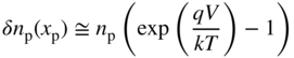
5
p–n Junction Solar Cells
- 5.1 Introduction
- 5.2 Light Absorption
- 5.3 Solar Radiation
- 5.4 Solar Cell Design and Analysis
- 5.5 Thin Solar Cells, G = 0
- 5.6 Thin Solar Cells, G > 0
- 5.7 Solar Cell Generation as a Function of Depth
- 5.8 Surface Recombination Reduction
- 5.9 Solar Cell Efficiency
- 5.10 Silicon Solar Cell Technology: Wafer Preparation
- 5.11 Silicon Solar Cell Technology: Solar Cell Finishing
- 5.12 Silicon Solar Cell Technology: Advanced Production Methods
- 5.13 Thin‐Film Solar Cells: Amorphous Silicon
- 5.14 Telluride/Selenide/Sulphide Thin‐Film Solar Cells
- 5.15 High‐efficiency Multi‐junction Solar Cells
- 5.16 Concentrating Solar Systems
- 5.17 Summary
- References
- Further Reading
- Problems
5.1 Introduction
We are now in a position to focus specifically on p–n junctions designed as solar cells for photovoltaic (PV) electricity production. In this chapter, we will study the basic operation of inorganic p–n junctions specifically designed and optimised for solar cells. Since silicon is the most important PV material we will focus on silicon; however, important alternative inorganic materials and their device structures will be introduced as well. The physics of the p–n junction solar cell is common to a wide range of semiconductor materials and is presented first in this chapter. Organic solar cells are currently being developed and dramatic progress is taking place in this field, which is presented in Chapter 7.
Solar cells may be small, such as the solar cells in rechargeable pocket calculators; however, the more important large‐scale deployment of solar cells for electricity production is now underway and as a result the PV industry is experiencing very high growth rates. Since 2002 PV production has been increasing by an average of more than 20% annually. At the end of 2017 the cumulative global PV installation capacity approached 400 GW. PVs has become the fastest growing sector of the energy production industry. The global solar cell market is expected to expand to nearly 70 GW yr−1 in 2017, up from 7.7 GW y−1 in 2009.
Bulk crystalline silicon solar panels currently dominate the market. Thin‐film solar cells have a small but continuing presence in the industry with approximately 5% of the market. Bulk silicon costs are dropping steadily and solar cells may now be produced at a cost of under US $0.35 W−1.
The solar cell functions as a forward‐biased p–n junction; however, current flow occurs in a direction opposite to a normal forward‐biased p–n diode. This is illustrated in Figure 5.1. Light that enters the p–n junction and reaches the depletion region of the solar cell generates electron–hole pairs (EHPs). The generated minority carriers will drift across the depletion region and enter the n‐ and p‐regions as majority carriers as shown. It is also possible for EHPs to be generated within about one diffusion length on either side of the depletion regions and through diffusion to reach the depletion region, where drift will again allow these carriers to cross to the opposite side. It is crucial to minimise carrier recombination, allowing carriers to deliver as much as possible of the available energy to the external circuit. This means that the carriers must cross the depletion region and become majority carriers on the opposite side of the junction. If they are generated and recombine on the same side of the junction they will not contribute to the flow of current.

Figure 5.1 Band diagram of a solar cell showing the directions of carrier flow. Generated electron–hole pairs drift across the depletion region. e, electron; h, hole
The available energy may also be optimised by minimising the potential barrier q(V 0 − V) that is required to facilitate carrier drift across the depletion region. The magnitude of q(V 0 − V) is subtracted from the semiconductor bandgap, which reduces the available energy difference between electrons and holes travelling in the n‐type and p‐type semiconductors, respectively. This causes a reduction in the operating voltage of the solar cell. If q(V 0 − V) is too small, however, excessive diffusion current will flow in the direction opposite to the desired drift current.
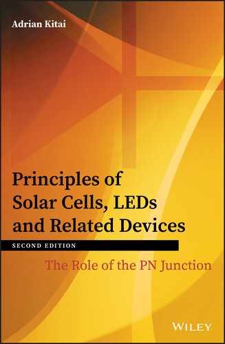
A useful way to think about solar cell operation is as follows: A p–n junction exhibits current–voltage behaviour as in Figure 3.7. If the p–n junction is illuminated in the junction region, then in reverse bias the reverse current increases substantially due to the EHPs that are optically generated. Without optical generation, the available electrons and holes that comprise reverse saturation current are limited to thermally generated minority carriers, which are low in concentration.
In forward bias the reverse current still flows but it is usually smaller than diffusion current. In a solar cell, however, the optically generated current is larger than diffusion current and it continues to dominate current flow until stronger forward‐bias conditions are present. The I–V characteristic of a solar cell is shown in Figure 5.2. The appropriate operating point for a solar cell is shown in which current flows out the positive terminal of the p–n junction (p‐side), through the external circuit, and then into the negative (n‐side) terminal. At this operating point the current flow is still dominated by optically generated carrier drift rather than by majority carrier diffusion.
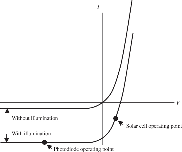
Figure 5.2
The  characteristic of a solar cell or photodiode without and with illumination. The increase in reverse current occurs due to optically generated electron–hole pairs that are swept across the depletion region to become majority carriers on either side of the diode
A photodiode is a light detector that operates in reverse bias, as shown in Figure 5.2. In this case, current flow is in the same direction as for solar cells, but energy is consumed rather than generated because they are reverse‐biased. Photodiodes are closely related to solar cells in spite of their energy‐consuming mode of operation and are important as optical detectors used in applications such as infrared remote controls and optical communications.
5.2 Light Absorption
In order to efficiently generate EHPs in a direct‐gap solar cell, light must reach the junction area and be absorbed effectively. Total energy will be conserved during the absorption process. Photons have energy E = hν, which must be at least as large as the semiconductor bandgap.
Total momentum will also be conserved. Photon momentum p photon = h/λ is very small compared to electron and hole momentum values in typical semiconductors. From Figure 2.8, for example, the band states range in momentum p = ℏk from p = 0 to p = ±(ℏπ/a). Since the lattice constant a is generally in the range of a few angstroms whereas visible light has wavelengths λ in the range of 5000 Å, it is clear that p photon is much smaller than the possible electron and hole momentum values in a band. The absorption coefficient for a given photon energy therefore proceeds as an almost vertical transition, as illustrated in Figure 5.3. This was discussed in detail in Chapter 4.

Figure 5.3 The absorption of a photon in a direct‐gap semiconductor proceeds in an almost vertical line since the photon momentum is very small on the scale of the band diagram. There are many possible vertical lines that may represent electron–hole generation by photon absorption as shown. These may exceed the bandgap energy
Photon absorption for a direct‐gap semiconductor was obtained in Eq. (4.24), and therefore
where A is a constant that depends on the material. Examples of direct‐gap semiconductors are shown in Figure 2.14. These include the III–V semiconductor gallium arsenide and the II–VI semiconductor cadmium telluride. Several other important direct‐gap solar cell semiconductor materials will be discussed later in this chapter.
In indirect‐gap semiconductors, the direct absorption of a photon having energy hν ≈ E g is forbidden due to the requirement of momentum conservation and is illustrated in Figure 5.4 and discussed in Section 2.13. Absorption is possible, however, if phonons are available to supply the necessary momentum. Typical phonons in crystalline materials can transfer large values of instantaneous momentum to an electron since atomic mass is much higher than electron mass. Phonon energies are small, however. At temperature T the phonon energy will be of the order of kT, or only 0.026 eV at room temperature. The absorption process involving a phonon is a two‐step process, as shown in Figure 5.4, along with a single‐step absorption for higher energy photons. The result is a low but steadily increasing absorption coefficient as photon energy increases above E g followed by a much steeper increase in absorption, once photon energies are high enough for direct absorption.
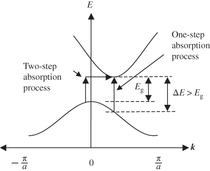
Figure 5.4 Indirect‐gap semiconductor showing that absorption near the energy gap is only possible if a process involving phonon momentum is available to permit momentum conservation. The indirect, two‐step absorption process involves a phonon to supply the momentum shift that is necessary to absorb photons. For higher energy photons, one of many possible direct absorption processes is shown.
The absorption coefficients for a number of important semiconductors are shown in Figure 5.5. Note the long absorption tails for silicon and germanium, which are indirect‐gap materials. The other semiconductors are direct‐gap materials that exhibit much sharper absorption edges.
Figure 5.5 Absorption coefficients covering the solar spectral range for a range of semiconductors. Note the absorption tails in silicon and germanium arising from two‐step absorption processes. Amorphous silicon is a non‐crystalline thin film that has different electron states and hence different absorption coefficients compared with single‐crystal silicon.
Note that absorption curves for Si, Ge, GaAs and CdTe are consistent with their band diagrams shown in Figure 2.17.
5.3 Solar Radiation
Sunlight is caused by blackbody radiation from the outer layer of the sun. At a temperature of approximately 5250 °C, this layer emits a spectrum as shown in Figure 5.6, which represents the solar spectrum in space and is relevant to solar cells used on satellites and space stations. Terrestrial solar cells, however, rely on the terrestrial solar spectrum, which suffers substantial attenuation at certain wavelengths. In particular, water molecules absorb strongly in four infrared bands between 800 and 2000 nm as shown.

Figure 5.6 Solar radiation spectrum for a 5250 °C blackbody, which approximates the space spectrum of the sun, as well as a spectrum at the earth's surface that survives the absorption of molecules such as H2O and CO2 in the earth's atmosphere. Note also the substantial ozone (O3) absorption in the UV part of the spectrum.
Source: Reproduced from www.global warmingart.com/wiki/File:Solar_Spectrum_png. Copyright 2011. globalwarmingart.com
5.4 Solar Cell Design and Analysis
The design of a practical silicon solar cell can now be considered. In order for light to reach the junction area of the p–n junction, the junction should be close to the surface of the semiconductor. The junction area must be large enough to capture the desired radiation. This dictates a thin n‐ or p‐region on the illuminated side of the solar cell. A significant challenge is to enable the thin region to be sufficiently uniform in potential to allow the junction to function over its entire area. If a contact material is applied to the surface of the cell, sunlight will be partly absorbed in the contact material. The common solution to this is to make the thin region of the silicon as conductive as possible by doping it heavily. In this way, the highly doped thin region simultaneously serves as a front electrode with high lateral conductivity (conductivity in a plane parallel to the plane of the junction) and as one side of the p–n junction. Since n‐type silicon has higher electron mobility and therefore higher conductivity than is achieved by the lower mobility of holes in p‐type material, the thin top layer in silicon solar cells is frequently n‐type in practice.
A crystalline silicon solar cell is shown in Figure 5.7. It consists of a thin n+ front layer. A metal grid is deposited on this layer and forms an ohmic contact to the n+ material. The areas on the n+ front layer that are exposed to sunlight are coated with an anti‐reflection layer. The simplest such layer is a quarter wavelength in thickness such that incident light waves reflecting off the front and back surfaces of this layer can substantially cancel each other (see Problem 5.3). The metal grid does block some sunlight; however, in practice the grid lines are narrow enough to prevent excessive light loss. A thick p‐type region absorbs virtually all the remaining sunlight, and is contacted by a back metal ohmic contact.
Figure 5.7
Cross‐section of a silicon solar cell showing the front contact metal grid that forms an ohmic contact to the n+‐layer. The depletion region at the junction has width 
Since most of the photons are absorbed in the thick p‐type layer, most of the minority carriers that need to be collected are electrons. The goal is to have these electrons reach the front contact. There will, however, also be some minority holes generated in the n+ region that reach the p‐region.
Sunlight entering the solar cell will be absorbed according to the relationship introduced in Section 2.13.
In order to simplify the treatment of the solar cell, we will assume that the optical generation rate G is uniform throughout the p–n junction. This implies that the absorption constant α is small. Real solar cells are approximately consistent with this assumption for photons of longer wavelengths of sunlight very close in energy to the bandgap. Shorter wavelengths, however, should really be modelled as a rapidly decaying generation rate with depth. We will return to this issue in Section 5.7.
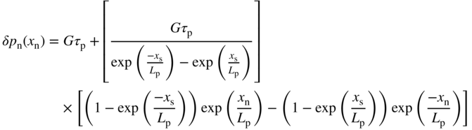
We will also start by assuming that the relevant diffusion lengths of minority carriers in both the n‐type and p‐type regions are much shorter than the thicknesses of these regions. This means that the p–n junction may be regarded as possessing semi‐infinite thickness as far as excess minority carrier distributions are concerned, and in Figure 5.7 the front surface and back surface at x n = x s and x p = x b, respectively, are far away from regions influenced by the junction.
For the n‐side, the diffusion equation (2.66a) for holes may be rewritten as

The term G must be subtracted from the hole recombination rate ![]() because
G
is a hole generation rate. The solution to this equation where
because
G
is a hole generation rate. The solution to this equation where
is

Note that the solution is the same as Eq. (2.67a) except for the added term Gτ p. See Problem 5.4.
The boundary conditions we shall satisfy are:

and
The first boundary condition is as discussed in Section 3.5. The dynamic equilibrium in the depletion region still determines the carrier concentrations at the depletion region boundaries. For the second boundary condition Gτ p is the excess carrier concentration optically generated far away from the depletion region (see Eq. (2.53)).
Substituting these two boundary conditions into Eq. 5.2 we obtain (see Problem 5.4)
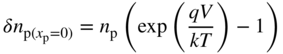
The analogous equation for the p‐side is

Note that if V = 0, Eqs. 5.3a and 5.3b yield δ p n(x n) = Gτ p and δ n p(x p) = Gτ n for large values of x n and x p, respectively. In addition, at V = 0 these equations give zero for both δ p n(x n = 0) and δ n p(x p = 0). We can show this more clearly in Figure 5.8 for an illuminated p–n junction under short‐circuit conditions (V = 0). We use Eq. 5.3a to plot p(x n) = δp(x n) + p n and n p(x p) = δn p(x p) + n p, where p n and n p are the equilibrium minority carrier concentrations.

Figure 5.8
Concentrations are plotted on a log scale to allow details of the minority carrier concentrations as well as the majority carrier concentrations to be shown on the same plot. Note that the n+‐side has higher majority carrier concentration and lower equilibrium minority carrier concentration than the more lightly doped p‐side corresponding to Figure 5.7. Diffusion lengths are assumed to be much smaller than device dimensions. The p–n junction is shown in a short‐circuit condition with 
Having determined the minority carrier concentrations we can now determine diffusion currents I n(x) and I p(x) using the equations for diffusion currents (Eqs. (2.56)). By substitution of Eqs. 5.3a and 5.3b into Eqs. (2.56) we obtain,

for holes diffusing in the n‐side and

for electrons diffusing in the p‐side (see Problem 5.5). Note that the first terms in these equations are identical with Eqs. (3.22b) and (3.22a) for an unilluminated diode.
Using Eqs. 5.4a and 5.4b evaluated at either edge of the depletion region, the two currents that enter the depletion region and contribute to the total solar cell current are given by

and
Since there is uniform illumination, we need also to consider generation in the depletion region. We shall neglect recombination of EHPs since W is much smaller than the carrier diffusion lengths. This means that every electron and every hole created in the depletion region contributes to diode current. The generation rate G must be multiplied by depletion region volume WA to obtain the total number of carriers generated per unit time in the depletion region. Carrier current optically generated from inside the depletion region, therefore, becomes the total charge generated per unit time or
Although both an electron and a hole are generated by each absorbed photon, each charge pair is only counted once: one generated electron drifts to the n‐side metal contact, flows through the external circuit, and returns to the p‐side. In the meantime, one hole drifts to the p‐side metal contact and is available there to recombine with the returning electron.
It now follows that using Eqs. 5.5a, 5.5b, and 5.6, the total solar cell current I , defined by convention as a current flowing from the p‐side to the n‐side, is given by the sum of three currents:
No negative sign is required in front of I p(0) because the x n axis is already reversed. Using Eq. (3.23b) the total diode current I may be written as:

where I L, the current optically generated by sunlight, is
This confirms that Figure 5.2 is valid and the I–V characteristic is shifted vertically (by amount I L) upon illumination. Of the three terms in Eq. 5.7b, the second term is generally smallest due to small values of W compared to carrier diffusion lengths, and since electron mobility and diffusivity values are higher than for holes the first term will be larger than the third term. It is reasonable that diffusion lengths L n and L p appear in Eq. 5.7b: carriers must cross over the depletion region to contribute to solar cell output current. They have an opportunity to diffuse to the depletion region before they drift across it, and the diffusion lengths are the appropriate length scales over which this is likely to occur.
The solar cell short‐circuit current I SC can now be seen to be the same as I L by setting V = 0 in Eq. 5.7a. Hence,
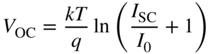
In addition, the solar cell open circuit voltage V OC can be found by setting I = 0 in Eq. 5.7a and solving for V to obtain

These quantities are plotted in Figure 5.9 together with the solar cell operating point.

Figure 5.9
Operating point of a solar cell. The fourth quadrant in Figure 5.2 is redrawn as a first quadrant for convenience. Open‐circuit voltage  and short‐circuit current
  as well as current
  and voltage
  for maximum power are shown. Maximum power is obtained when the area of the shaded rectangle is maximised
The fill factor FF is defined as

In crystalline silicon solar cells FF may be in the range of 0.7–0.85.
5.5 Thin Solar Cells, G = 0
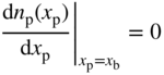
Since practical solar cells have a very thin n+ layer, as shown in Figure 5.7, and even the p‐side may be small in thickness, we will now take this into consideration in the device model. We will remove the restriction that the relevant diffusion lengths of minority carriers in both the n‐ and p‐type regions are much shorter than the thicknesses of these regions. This means that in Figure 5.7 the front surface and back surface at x n = x s and x p = x b, respectively, must be assigned suitable boundary conditions in order to calculate minority carrier concentrations.
We have discussed semiconductor surfaces in Section 2.20. We can apply Eq. (2.69b) to the front interface at x n = x s and we can write
where S f is the effective front surface recombination velocity, which is a modified value of surface recombination velocity because the front surface is not a free surface and surface states will be influenced by the anti‐reflection layer as well as the small areas occupied by the ohmic contacts. The minority carriers in the n+‐region are holes.
The back metal interface must also be modelled. As with the front surface, we will use an effective back surface recombination velocity S b to describe this and hence at the back surface,
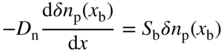
where the minority carriers in the p‐region are electrons.
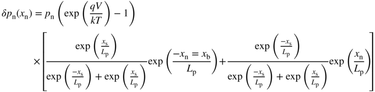
Consider the p‐type material as shown in Figure 5.7. At x p = 0 the excess minority carrier concentration in an unilluminated junction at voltage V is given from Eq. (3.20b) as

and at x p = x b, δn p will depend on the value of S b. If we examine the case in which S b is very large, then from Eq. 5.12 it follows that
These two boundary conditions may be substituted into the general solution of the diffusion equation for electrons. In Eq. (2.67a) we have written this for holes. For electrons it becomes
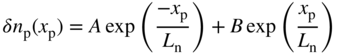
where ![]() . We now need to consider both terms since the length of the p‐type material is finite and we are not justified in assuming that B = 0. The two boundary conditions give us two equations:
. We now need to consider both terms since the length of the p‐type material is finite and we are not justified in assuming that B = 0. The two boundary conditions give us two equations:

and

Multiplying Eq. 5.14 by exp ![]() and subtracting it from Eq. 5.15 we can solve for A and obtain,
and subtracting it from Eq. 5.15 we can solve for A and obtain,

By multiplying Eq. 5.14 by exp ![]() we can similarly solve for B and obtain,
we can similarly solve for B and obtain,

Substituting A and B into Eq. 5.13 we obtain,
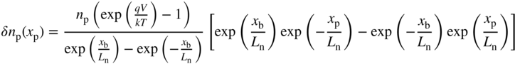
The identical method may be used to find the minority hole concentration in the n+ material. We will assume that S f is very large, which implies that
and we obtain,

Note that in the p‐side, ![]() and
δn
p(x
b) = 0 as expected. If we assume that
and
δn
p(x
b) = 0 as expected. If we assume that ![]() (the p‐region is much thinner than the diffusion length of minority electrons in the p‐side) we can apply a Taylor series expansion for small values of
α
(the p‐region is much thinner than the diffusion length of minority electrons in the p‐side) we can apply a Taylor series expansion for small values of
α
to all the exponential functions having arguments ![]() or
or ![]() in Eq. 5.16a. See Problem 5.14. The result is,
in Eq. 5.16a. See Problem 5.14. The result is,

The first two terms in the square brackets represent a straight line with negative slope, which satisfies the required boundary conditions ![]() and
δn
p(x
b) = 0. The second two terms in the square brackets add to zero at
x
p = 0 and at
x
p = x
b
and represent a positive parabola. This parabola is small in amplitude and is shown in Figure 5.10 superimposed on the straight line from the first two terms.
and
δn
p(x
b) = 0. The second two terms in the square brackets add to zero at
x
p = 0 and at
x
p = x
b
and represent a positive parabola. This parabola is small in amplitude and is shown in Figure 5.10 superimposed on the straight line from the first two terms.

Figure 5.10
Excess minority carrier concentrations for a solar cell having dimensions  and
and  that are small compared to the carrier diffusion lengths. Very high values of surface recombination velocity are present. Note that a forward bias is assumed, and there is no illumination. The straight dotted lines correspond to the first two terms in the square brackets of Eqs. 5.18a and 5.18b and the small parabolas that correspond to the second two terms in the square brackets are superimposed as solid lines
A similar analysis can be applied to the n‐side using Eq. 5.16b yielding

The resulting graph is also shown in Figure 5.10.
It is clear that the carrier concentrations of both minority electrons and minority holes decrease rapidly as we move away from either side of the depletion region. This means that minority diffusion fluxes are enabled that flow away from the junction. The thinner the solar cell becomes, the steeper these decreases become. Minority carriers flow in the opposite directions to the directions that we require: In a solar cell the minority carriers should flow towards the junction.
For this reason, thin solar cells having high values of S b and S f are inefficient. We will now examine a second limiting case in which S b and S f are assumed to be zero. If we examine the p‐side of the junction, then using Eq. (5.12) we can conclude that at the back surface,
Inserting this boundary condition along with the previous boundary condition of
into Eq. 5.13 and solving for A and B we obtain,
and

Therefore from Eq. (5.13) we have,

And in the n‐side we would obtain,
Note that if ![]() then, approximating
then, approximating ![]()
![]() ,
, ![]() and
and ![]() we obtain,
we obtain,
which shows that carrier concentration is independent of x p . Without the Taylor series approximation a more accurate plot would show that the carrier concentration would drop slightly away from the edge of the depletion region depending on x b/L n and x s/L p. See Problem 5.15. In the n‐side the analogous result is

These straight lines are shown in Figure 5.11 for a solar cell without illumination in a forward bias condition. Note that if the solar cell were connected to an electrical load and illuminated, the minority carrier concentrations would slope downwards towards the depletion region to approach (but not reach) the condition at V = 0 of Figure 5.8, and the generated minority carriers would have an opportunity to diffuse towards the junction without competition from surface recombination. The situation here is much more conducive to minority carrier flow towards the depletion region than that shown in Figure 5.10.
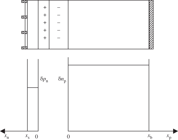
Figure 5.11
Excess minority carrier concentrations for a solar cell having dimensions  and
and  that are small compared to the carrier diffusion lengths. Zero surface recombination velocity is assumed, which means that there is little drop‐off of carrier concentrations towards the front and back surfaces. The graph shows the case for the approximation of Eq. 5.19a
The thickness of the solar cell must be sufficient to allow for adequate optical absorption of the sunlight. Techniques to minimise effective surface recombination velocities are important and will be discussed in Section 5.8.
5.6 Thin Solar Cells, G > 0
We can also consider the thin solar cell model to include a uniform generation rate G under short‐circuit conditions. The general solution of Eq. 5.2 rewritten for the p‐side of the solar cell gives us

From Section 5.5, the boundary conditions for the thin solar cell under short‐circuit conditions and a very high surface recombination velocity are

and
Applying these boundary conditions to Eq. 5.20 we have
and

Solving for A and B and substituting them back into Eq. 5.20 we obtain,

and in the n‐side we obtain,
Note that δn p(x p) = 0 at both x p = 0 and at x p = x b as required by the boundary conditions.
Once again we can use a Taylor series to approximate this. Substituting the first three terms of Taylor series ![]() for all the exponential functions in Eq. 5.21a (see Problem 5.16) we obtain,
for all the exponential functions in Eq. 5.21a (see Problem 5.16) we obtain,

and in the n‐side,

which again satisfy the boundary conditions and represent negative parabolas. A graph of this is shown in Figure 5.12. Note that minority electrons may diffuse in two directions since some portions of δn p(x p) have a positive slope and some portions have a negative slope. Only those electrons that reach the edge of the depletion region at x p = 0 will contribute to solar cell current. This clearly illustrates unwanted competition from the surface at x p = x b having high surface recombination velocity.

Figure 5.12
Plot of  versus
  using Eq. 5.22a with generation rate
  . The boundary conditions are for short‐circuit conditions and a very high surface recombination velocity at
  . The curve is a negative parabola
5.7 Solar Cell Generation as a Function of Depth
The efficiency of electron and hole pair collection in a solar cell can be analysed as a function of the depth at which carriers are generated by an absorbed photon. We can initially assume that generation occurs at only one depth, and then determine the probability that carriers are collected and cross over the junction. We will simplify the problem by assuming that:
- The solar cell is operating under short‐circuit conditions.
- The diffusion length is much smaller than the solar cell thickness.
Since most carriers are absorbed in the p‐type layer we will confine our attention to the p‐side of the junction, although the analysis may readily be extended to the n‐side and to the depletion region. The assumed generation rate will resemble a delta function, as shown in Figure 5.13. Note that although this situation is physically not realisable it does serve to illustrate how the ability to collect minority carriers depends on depth. We will also see that it leads to a method to derive solar cell current when generation rate G varies with depth.

Figure 5.13
Generation rate as a function of depth showing zero generation except at a specific depth 
For 0 ≤ x p ≤ x G, we can determine the carrier concentration using the diffusion equation and the general solution of Eq. 5.13:

Under short‐circuit conditions, excess carrier concentration at x p = 0 will be zero and hence
Now,
For x G ≤ x p ≤ x b the general solution to the diffusion equation will be
because the function must fall to zero for large values of x p. To be a continuous function we require that Eqs. 5.23 and 5.24 are equal at x p = x G and

Therefore,
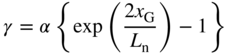
which may be used to replace γ in Eq. 5.24 resulting, for x G ≤ x p ≤ x b, in
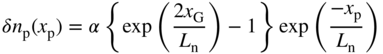
The functions δn p(x p) from Eqs. 5.23 and 5.25 are plotted in Figure 5.14.
Now the diffusion current density arising from these carrier concentrations may be calculated in the normal manner using

At x p = 0 the diffusion current is determined using the derivative of Eq. 5.23, and we obtain,

At x p = x G there are two components of the diffusion current, both flowing towards the generation zone at x p = x G. (The fluxes of excess electrons actually flow away from x G in the directions of decreasing carrier concentration; however, the currents flow in directions opposite to the fluxes.) The magnitudes of these currents are shown in Figure 5.14 and are determined using the slopes at x p = x G of Eqs. 5.23 and 5.25, respectively.

Figure 5.14
Generation rate, excess carrier concentration, and magnitude of the diffusion current density as a function of position in the p‐side of the solar cell. Note that the diffusion current is positive for  and negative for
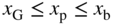
From Eq. 5.23 we obtain a current magnitude due to the electron flux flowing to the left of x G of
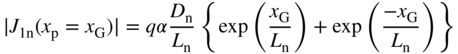
and using Eq. 5.25 we obtain a current magnitude due to electron flux flowing to the right of x G of
The total generated current density at x G is the sum of these two current magnitudes, or

The fraction η of this total current that reaches the depletion region is obtained by dividing Eq. 5.26 by Eq. 5.27 to yield:
This means that the contribution to the usable current flow decreases exponentially as a function of the distance between the depletion region and the position of EHP generation in the p‐type region. For optimum performance in solar cells of semi‐infinite thickness (x b > L n), we therefore require that the absorption depth of photons is smaller than the diffusion length L n.
This analysis is very powerful since it allows us to calculate the total current reaching the depletion region from a set of EHP generation sources at different depths. For example, consider the case of two sources as shown in Figure 5.15: A silicon solar cell operates with generation rates G1 at depth x 1 and G2 at depth x 2 .

Figure 5.15
EHP generation rate is  at depth
  and
and  and depth
The total minority electron current reaching the edge of the depletion region is the sum of the currents arising from each generation depth as calculated using a unique value of η from Eq. 5.28 for each depth. This approach which relies on the principle of superposition is valid for linear differential equations such as the diffusion equation we are using. See Problem 5.17.
This method can be extended to more than two sources to allow for the determination of total current available due to many generation depths and can therefore account for an exponential reduction of generation rate as a function of depth. This leads to solar cell models that are more realistic than the model of Section 5.4 that assumed a uniform generation rate. See Problem 5.18.
5.8 Surface Recombination Reduction
In silicon, diffusion lengths in the range of 1 mm are achievable. Since silicon wafers, well under 0.2 mm in thickness are cut and processed into solar cells in volume production it is clear that a low effective surface recombination velocity at the rear contact is required. Methods to reduce effective surface recombination velocity are called surface passivation techniques.
This may be achieved by forming a p+ doped region near the back contact. Figure 5.16 shows the resulting solar cell band diagram. A potential step near the back contact is formed that helps to prevent minority electrons from reaching the back silicon–metal interface due to the back surface electric field that is created at the step. Much lower effective rear surface recombination velocities result from this and the rear p+‐region is therefore part of standard solar cell design used for the majority of production bulk silicon solar cells achieving up to approximately 21% conversion efficiency.
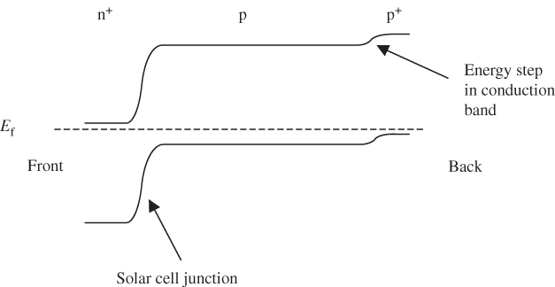
Figure 5.16 Back surface field formed by a p+‐doped region near the back of the solar cell. A potential energy step that generates a built‐in electric field decreases the likelihood of electrons reaching the back surface of the silicon
A yet more efficient solar cell design is called the passivated emitter and rear contact (PERC) solar cell that enables single‐crystal silicon solar cells that can achieve 21–25% conversion efficiency. The structure used is shown in Figure 5.17. Instead of the rear electrode making contact with the entire area of the silicon p‐type layer, it only makes spatially selective contact points and the majority of the back surface of the silicon is coated with electrically insulating and optically transparent oxide or nitride layers. The material in direct contact with the silicon will be silicon oxide. This material can be grown or deposited on the back of the cell to yield a highly passivated surface. The passivation is a consequence of a reduction in the density of dangling silicon bonds and hence a reduction in deep traps at the silicon–silicon oxide interface. Additional oxide and nitride layers may be deposited to optimise optical reflection off the back of the cell in conjunction with the aluminium rear contact. This reflection can thereby enable a longer total optical path length through the cell to increase the absorption of longer wavelengths of sunlight where the absorption coefficient is small. Note that the back surface field is still employed to minimise recombination at the contact points.

Figure 5.17 Passivated emitter and rear contact (PERC) solar cell. Oxide/nitride layers may include aluminium oxide and silicon nitride layers in addition to a thin silicon oxide layer that forms at the silicon surface. The p‐type material is often called the emitter because in normal operation it emits minority electrons towards the depletion layer
In order to obtain the very highest conversion efficiencies of close to 25% achievable in production silicon solar cells, the PERC design must be combined with several other optimisation measures including textured and anti‐reflection‐coated front surfaces as well as high‐purity, long‐carrier‐lifetime silicon. See Section 5.10. Provided the additional costs for these cells can be managed they will increasingly penetrate the silicon solar cell market.
5.9 Solar Cell Efficiency
There are some fundamental constraints that set an upper limit on the efficiency that can be achieved from a single‐junction solar cell.
There are two major contributions to efficiency loss in p–n junction solar cells that arise from optical absorption of the solar spectrum. The first arises from photons having energies lower than E g. These photons are not absorbed and do not contribute to current output. The second loss arises from photons having energy higher than E g. The extra photon energy in excess of E g becomes carrier kinetic energy, which quickly gets converted to heat as the carriers relax or thermalise to their lower energy states within the band. This happens before the carriers can be collected and utilised. These two efficiency loss processes would not be an issue if the solar spectrum was monochromatic, but the broad blackbody solar spectrum immediately limits efficiency values to under 50% for a single‐junction solar cell.
A third loss results from the discrepancy between the optimum operating voltage V
MP and the bandgap E
g of the semiconductor used. A minimum photon energy corresponding to E
g is needed to create EHPs; however, V
MP is less than E
g. For example, in silicon, ![]() , or about 55%. The open circuit voltage V
OC should be as large as possible for maximum efficiency. From Eq. 5.9,
, or about 55%. The open circuit voltage V
OC should be as large as possible for maximum efficiency. From Eq. 5.9,
which means that I
0 should be as small as possible. It also means that
I
SC
should be as large as possible. We can rewrite I
0 from Eq. (3.23), and using ![]() and
and ![]() we obtain,
we obtain,
which clearly shows the sensitivity of I 0 on n i. Using Eq. (2.39),

we see that n i decreases exponentially as energy gap E g increases and as T decreases. This therefore limits the maximum value of V OC.
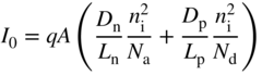
If the intensity of solar radiation is increased by focusing sunlight onto a solar cell, there will be a proportional increase in I SC = I L . But from Eq. 5.9, V OC will also increase and hence overall efficiency increases. Efficiency analysis is dominated by the three loss mechanisms just described and the result is well‐known as the Shockley–Queisser limit. As expected, there is an optimal energy gap for a solar cell as shown in Figure 5.18. The limiting efficiency of a single‐junction solar cell is approximately 30% for 1 sun of solar radiation and rises to approximately 37% for 1000 suns. Energy gaps of a number of semiconductors are also indicated. The practical overall efficiency of a single‐junction solar cell under 1 sun will be under 30%. Silicon solar cells have reached approximately 26% efficiency for 1 sun in the lab, and 24–25% in production. GaAs‐based solar cells having a slightly more optimal direct gap have reached higher values of 28–29%.
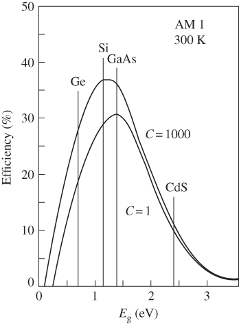
Figure 5.18 Efficiency limit of solar cells based on a number of well‐known semiconductors. Note the increase in efficiency potentially available if the sunlight intensity is increased to 1000 times the normal sun intensity.
Source: Sze (1985). Copyright 1985. Reprinted with permission from John Wiley & Sons
Figure 5.19 shows the trend towards higher efficiencies from a wide range of solar cell technologies as time progresses. Note that the highest efficiency solar cell types are multi‐junction solar cells that can exceed the Shockley–Queisser limit. These will be covered in Section 5.15. Most production crystalline silicon solar cells are in the range of 16–24% efficient.
Figure 5.19 Best research solar cell efficiencies achieved in a given year.
Source: Courtesy of United States Department of Energy, Property of the U.S Federal Government. Data compiled by National Renewable Energy Laboratory (NREL)
Solar cell efficiency also depends on the operating temperature of the solar cell p–n junction. In general, there will be a decrease in efficiency at higher temperatures due to the increase in I 0. This means that it may be advantageous to generate solar power at higher latitudes where ambient temperatures are lower. The disadvantage, however, is the lower angle of the sun relative to locations near the Equator. See Example 5.2.
5.10 Silicon Solar Cell Technology: Wafer Preparation
The most widely manufactured solar cells are based on the use of silicon. There are three main types of silicon solar cell materials. They are single‐crystalline silicon, multicrystalline silicon, and amorphous silicon. Each material has a strong niche in the solar cell market, but the performance levels and other attributes differ dramatically. The manufacture and design aspects of silicon‐based solar cell types will be reviewed in this chapter, and solar cells made using other materials will be covered in Sections 5.13-5.15.
Single‐crystal silicon cells have efficiency values that can well exceed 20% in production. The starting materials must be highly purified. To achieve the highest purity of silicon, naturally occurring quartz (SiO2) is reduced by the reaction:
The reaction occurs in a furnace in which carbon in the form of coke is introduced along with the SiO2 at temperatures well above 1414 °C, which is the melting point of silicon. In addition, to react and remove aluminium and calcium in the silicon, oxygen is blown into the furnace. The resulting metallurgical grade silicon, or MG silicon, is 98–99% pure and typically contains atomic percentages of metal impurities in the range of 0.3% Fe, 0.3% Al, 0.02% Ti, and under 0.01% of each of B, Cr, Mn, Ni, P, and V. There is also some residual oxygen incorporated.
To achieve semiconductor grade silicon, further purification is required. The standard process is the Siemens process. Fine MG silicon powder is reacted with HCl to produce gaseous trichlorosilane through the reaction:
The trichlorosilane (melting point −126.2 °C, boiling point 31.8 °C) is condensed to a liquid and then distilled several times to upgrade its purity. Upon reacting it with hydrogen at elevated temperature, the reduction reaction
takes place at the hot surface of a high‐purity silicon rod. The rod is continuously coated with the resulting semiconductor grade silicon in the form of a fine‐grained polycrystalline deposit. Eventually thicknesses of silicon in the range of 10 cm may be deposited onto the rod. The purity available is in the parts per billion range, and the semiconductor industry relies on this process for its supply of silicon.
This process is high in energy consumption, involves environmentally hazardous chloride chemistry and adds significantly to the ultimate cost of silicon solar cells. In spite of this, it remains the dominant process used for the final purification of standard solar‐grade silicon in the industry.
There are lower cost processes that have been developed to partially purify MG silicon. For example, MG silicon may be mixed with aluminium and a molten solution of silicon and aluminium may be cooled to precipitate purified crystalline platelets of silicon having purity in the parts per million range. The aluminium phase may be removed from the platelets by melting it and pouring it off, followed by an acid‐washing step in which remaining aluminium is dissolved away. Further purification can then be carried out as required.
The purity requirement of solar‐grade silicon is lower than that for semiconductor grade silicon, and the purification process may be optimised to provide adequate solar cell performance. This depends on the desired specifications of the solar cells, which range from 14 to 24% efficiency. The precise optimisation of the purification process is a highly competitive aspect of solar cell manufacturing and is typically not disclosed by manufacturers. The resulting silicon is called solar‐grade material. Regular measurement of minority carrier lifetime during production is an important and very useful probe of the impurity level achieved since this lifetime is highly sensitive to impurity concentration. See Section 3.8.
The highest efficiency silicon solar cells are single crystal. Solar‐grade silicon is melted and a suitable concentration of boron is intentionally added to produce the p‐type silicon required for the thick p‐type layer of the solar cell of Figure 5.7. A single‐crystal silicon seed is lowered to the liquid surface and slowly pulled from the melt, resulting in the growth of a single‐crystal boule or circular rod of single‐crystal silicon having a diameter in the 15–20 cm range and a length of 1–2 m. This is known as the Czochralski growth process (see Figure 5.20).

Figure 5.20 Czochralski growth system.
Source: Reprinted from http://www.learningelectronics.net/vol_3/chpt_2/12.html. Learning Electronics
The boule is then sliced into silicon wafers that are approximately 150 μm (0.15 mm) thick using a wire saw process. An array of closely spaced, tensioned metal wires is continuously pulled against the side of a silicon boule in the presence of an abrasive slurry. The rubbing action of the wire against the boule wears away the silicon and a series of cuts is made. The kerf of these cuts is primarily determined by the diameter of the wire and may be in the range of 100 μm. Hundreds of silicon wafers may be cut at one time as the array of wires slowly passes through the boule. The advantages of this process include the low stress caused by any one wire, which prevents damage to the silicon, and the ability to prepare a large number of wafers per cycle. The steady replacement of the abrasive slurry is provided by a pumping system, which ensures that the cutting speed is maintained. A disadvantage of this cutting process is the loss of approximately 50% of the available silicon. In spite of this loss the wire saw approach is the predominant silicon wafering method and it is improving steadily. Over the past decade, the ability to cut thinner wafers has progressed through improvements to all aspects of this process. Wafers have reduced in thickness from 300 μm to under 200 μm, and there is an opportunity to reduce this further to approach the limiting 100 μm thickness required for absorption of sunlight in silicon. Slurries containing diamond abrasives can further improve cutting speed and quality. It is also interesting to note that whereas the semiconductor industry currently uses 30 cm diameter boules of silicon and wafer thicknesses of 300–600 μm, the solar cell industry has maintained its use of smaller diameter boules since they assist in the reduction of wafer thickness and also prevent excessive electric currents being generated in a single silicon wafer.
The market share of multicrystalline silicon in solar cells has grown to rival the use of single‐crystal silicon. This is a result of cost reduction associated with the elimination of the Czochralski growth process as well as a steady improvement in the efficiency of multicrystalline silicon solar cells, which are typically in the range of 15–20% efficient versus 18–25% for single‐crystal silicon. Rather than pulling a single crystal from the melt, a casting process is used in which molten solar‐grade silicon is poured into a mould. Solidification takes place in a very slow and controlled manner to optimise the growth of very large grained silicon. Grain sizes in the range of 1 cm may be achieved. Square cross‐section ingots of multicrystalline silicon formed in this manner may be sliced using wire saws to produce square silicon wafers. The square wafers may be assembled into solar cell modules more efficiently than the wafers from the single‐crystal process. After cutting, the wafers may be polished and are then ready for cell fabrication steps. Multicrystalline silicon is shown in Figure 5.21.
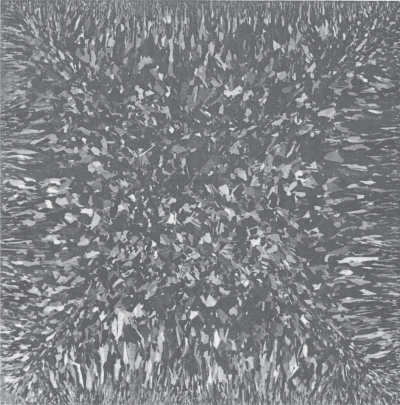
Figure 5.21 A 10 × 10 cm2 multicrystalline silicon wafer. Note the large single‐crystal grains that can be up to approximately 1 cm in dimension.
Source: Green (1981). Copyright 1981. Reprinted with permission from M. A. Green
The grain boundaries of multicrystalline silicon must be treated to make them behave like low recombination velocity surfaces. In the p‐type material it is therefore appropriate to introduce p+ doping into the grain boundaries. This forms the equivalent of a back surface field at each grain boundary. Elements such as boron or aluminium can be used, provided they are preferentially introduced into the grain boundaries of the multicrystalline silicon by either grain boundary diffusion or grain boundary segregation.
5.11 Silicon Solar Cell Technology: Solar Cell Finishing
An important and widely used first step achieves texturing of the silicon surface. If the silicon wafers are cut with (100) orientation, a selective etch may be used to achieve a surface covered with square‐based pyramids of silicon, as shown in Figure 5.22. These pyramids are typically 10 μm high and improve the light absorption of the silicon surface. Light reaching the silicon surface may enter the solar cell through the pyramid side facets or it may reflect off the side facet of one pyramid and enter the solar cell through another pyramid as shown.

Figure 5.22 The possible paths of light beams reaching the solar cell surface are shown. At least two attempts to enter the silicon are achieved for each light beam. The angle of the sides of the pyramids may be calculated from the known crystal planes of silicon
Silicon solar cells are bonded behind low‐iron‐content, high‐transmission solar‐grade glass using transparent polymer bonding material that is capable of filling in voids between the silicon and the glass. Iron impurities found in standard float glass absorb sunlight and solar‐grade glass therefore has lower iron content to improve solar panel efficiency. The reflectivity of sunlight off an untreated silicon surface embedded in a polymer behind a glass plate is approximately 20%. If, on average, every reflected light beam is directed back to the silicon surface once again, as shown in Figure 5.22, then the reflectivity is reduced to 20% × 20% = 4%, which is achieved in practice. Even lower reflectivity may be obtained using an anti‐reflection coating; however, this would be applied after other fabrication steps are complete. A micrograph of pyramids formed in an etched silicon surface is shown in Figure 5.23.
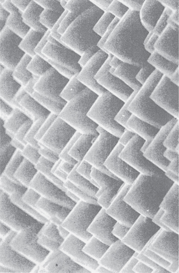
Figure 5.23 Micrograph of pyramids selectively etched in the surface of a (100) silicon wafer. Sides of the pyramids are {111} planes, which form automatically in, for example, a dilute NaOH solution. Note the scale showing that the pyramids are approximately 10 μm in height although there is a range of pyramid heights. The pyramids are randomly placed on the surface; however, they are all orientated in the same direction due to the use of single‐crystal silicon.
Source: Green (1981). Copyright 1981. Reprinted with permission from M. A. Green
Once the desired texturing is complete the front surface of the wafer must be doped n‐type. This requires a phosphorus diffusion, which may be achieved using commercially available printable paste containing phosphorus, which is applied using a screen printing process to the front surface of the wafer. A paste having a suitable viscosity is deposited on the surface of a fine mesh or screen. The silicon wafer is placed just below but not touching the screen, and a flexible blade is passed over the screen forcing contact between the wafer and the screen and causing a well‐controlled layer of paste to pass through the screen and onto the wafer. After a low‐temperature bake, the volatile components of the paste are released leaving only the desired phosphorus on the silicon. A high‐temperature diffusion step is then used to diffuse the phosphorus to the desired depth in the silicon, which is typically set to form the p–n junction about 1 μm below the surface. The result is an n+‐layer with N d > 1018 cm−3 near the front surface.
The back contact for a standard back surface field solar cell is achieved using an aluminium dopant that forms a p+‐doped layer. This layer serves two functions. It creates the back surface field for a low recombination velocity back surface, and it also allows for a tunnelling‐type ohmic contact to the back aluminium metal contact. Commercially available aluminium pastes are available that contain the aluminium in a paste suspension. A low‐temperature bake volatilises the unwanted components and subsequently the aluminium is diffused into the silicon in a high‐temperature anneal.
Silver paste containing a small percentage of aluminium is also available, which forms a silver back metallisation. This permits soldering to the back of the solar cell during module manufacture. The screen printing method allows the silver paste to be deposited selectively onto small areas of the back of the wafer, which is done to enable soldering while minimising the amount of silver required. If the screen is only porous in the areas in which a deposit is desired, then when the rubber blade is passed over the screen during printing, paste is only applied to the silicon in these areas. Such screens are prepared with a spatially patterned polymer masking layer that blocks the pores of the screen in selected areas. A suitably masked screen may be used to print a given pattern onto thousands of wafers.
The front contact of the solar cell may now be printed. This requires a set of narrow conductors that are typically connected by bus bars, as shown in Figure 5.24. Since light loss increases with front contact area, conductor width must be minimised and is routinely in the range of 200 μm. Spacing between the conductors is determined by the sheet resistance of the n+ layer. The sheet resistance depends upon the phosphorus doping level, which is optimised to avoid excessive doping levels that exceed the solubility limit of the dopant in the silicon. The thickness of the n+ layer must also be minimised to reduce light absorption in the n+ silicon. Since the front surface recombination velocity of the solar cell is typically high, it is better to absorb the bulk of the light in the depletion layer and in the p‐type silicon layer.

Figure 5.24 Pattern of conductors used for the front contacts of a silicon solar cell showing bus bars as well as the narrow conducting fingers. The electrode was screen‐printed.
Source: https://en.wikipedia.org/wiki/Solar_cell#/media/File:Solar_cell.png
As a result there is an upper practical limit to the conductivity achievable in the n+ layer. This is defined by the sheet resistance R s of the layer, expressed in units of ohms, where
ρ and T being layer resistivity and layer thickness respectively. R s is the resistance of a square unit of the layer measured across conductive contact strips running along two opposing edges of the square unit. The value of R s determines the spacing between the narrow conductors. A typical spacing is approximately 3 mm, as shown in Figure 5.24. An effective method of forming these contacts is through the use of silver‐based paste containing n‐type dopant phosphorus to ensure a good ohmic contact. The paste is screen‐printed through a suitable masked screen. The narrow conductors and bus bars may then be printed in one step. As with the back contact metallisation, low‐ and then high‐temperature annealing steps are performed.
An anti‐reflection layer applied to silicon solar cells should have a thickness of
λ/4 and a refractive index of ![]() where n
Si and n
polymer are the indices of refraction of the silicon and the polymer bonding material. A suitable material is TiO
x
, which is usually deposited by sputtering. See problem 5.3.
where n
Si and n
polymer are the indices of refraction of the silicon and the polymer bonding material. A suitable material is TiO
x
, which is usually deposited by sputtering. See problem 5.3.
The solar cell is now ready for soldering to conductors. Bonding and packaging materials for cell mounting onto a front glass substrate have been well developed for this process. A completed solar module containing multiple wafers and capable of withstanding the outdoor environment for over 25 years is the result.
5.12 Silicon Solar Cell Technology: Advanced Production Methods
Since by far the majority of solar cells are made from crystalline silicon, it is not surprising that a variety of production techniques have been developed and implemented in order to lower the cost of production.
Single‐crystal silicon continues to lead in silicon solar cell efficiency. This is partly due to a purification process that is inherent in the Czochralski growth process: impurities in the molten feedstock segregate into the remaining liquid silicon since the liquid has a higher solubility for impurities than the crystalline material. The crystallised silicon is therefore higher in purity than the feedstock. The most important impurity is generally iron, and impurity levels below 1012 atoms cm−3 of iron are required to achieve carrier diffusion lengths well above 150 μm. The speed of Czochralski growth may be increased beyond the speed used in the microelectronics industry to values in the range of 1 mm min−1. The resulting carrier diffusion length is carefully monitored and process speed is optimised to minimise cost. The simplicity of the growth method allows for highly repeatable and dependable growth of high‐quality silicon. In multicrystalline silicon typical ingot sizes have reached over 250 kg. Wafer thicknesses of approximately 150 μm are standard. In polycrystalline solar cells the casting of silicon does not permit this purification process and the purity of the feedstock is more carefully controlled.
Although the boule and ingot‐based methods of silicon wafer production are well developed and are the dominant methods of production of silicon solar cells, they both require sawing with the associated material loss. An interesting alternative to this is silicon ribbon technology, which results in the direct solidification of molten silicon into thin silicon sheets or ribbons. The best‐known approach is called the string ribbon growth method. Two parallel strings separated by several centimetres are pulled vertically through a crucible of molten silicon. As the liquid wets the strings, a thin web of liquid is maintained between the strings through surface tension, which solidifies into a polycrystalline silicon sheet upon cooling, as shown in Figure 5.25.

Figure 5.25 String ribbon growth of a silicon ribbon. Surface tension in liquid silicon forms a silicon sheet upon cooling. Thickness of the ribbon is controlled by pull rate and rate of cooling of the silicon web.
Source: Luque and Hegedus (2003). Copyright 2003. Reprinted with permission from John Wiley & Sons
Challenges associated with silicon ribbon growth include:
- removal of the strings by cutting off the edges of the ribbon;
- the degree of flatness achievable in production;
- the ultimate solar cell performance;
- impurity incorporation due to the molten silicon in contact with its container;
- the energy used in maintaining molten silicon temperatures during pulling;
- the low production rate per pull due to the small cross‐sectional ribbon area compared to conventional Czochralski boule growth.
Cell efficiency is in the range of 14%, which is lower than wafered cells due to the incorporation of impurities and the multicrystalline nature of the ribbon. Ribbon‐grown silicon solar cells are no longer commercially available.
5.13 Thin‐Film Solar Cells: Amorphous Silicon
There are strong driving forces to lower production costs of solar cells. There is a keen desire to further reduce the cost of solar cells to compete effectively with traditional fossil fuels and nuclear power. The most important approach to lowering cost is thin‐film PV. Rather than bulk or ribbon growth of the active material, thin films of semiconductor layers are deposited on a substrate that supports the thin films. The substrate is low in cost and becomes an integral part of the finished product.
In the early 1970s the semiconductor properties of a new form of silicon were discovered. Known as amorphous silicon, often written a‐Si, this is a disordered form of silicon, generally prepared in thin‐film form. The normal long‐range bonding in silicon becomes disordered or random; however, local bonding remains largely tetrahedral as in single‐crystal material. This a‐Si material may be grown in thin‐film form onto a supporting substrate.
Several percent of the tetrahedral silicon bonds are incomplete or dangling due to the lack of long‐range order. If a suitable amount of hydrogen is incorporated with the a‐Si thin‐film, hydrogen atoms effectively complete or terminate these silicon bonds. The optimum incorporation of hydrogen turns out to be achieved using a growth technique known as plasma‐enhanced chemical vapour deposition (PECVD), in which a gas mixture of SiH4 (silane) and H2 is subjected to an RF (radio frequency) discharge, which breaks the molecules apart to form radicals. These radicals then deposit onto a substrate placed in the discharge resulting in the growth of the desired thin film on the substrate. The resulting hydrogen‐terminated film is known as a‐Si:H material. The atomic structure of a‐Si:H is shown in Figure 5.26.

Figure 5.26 Atomic structure of a‐Si:H in which H atoms terminate dangling Si bonds, which are generally isolated but may also be clustered (two dangling bonds in one silicon atom).
Source: Luque and Hegedus (2003). Copyright 2003. Reprinted with permission from John Wiley & Sons
It is of significance that the absorption of sunlight in a‐Si:H is very different from the absorption in crystalline silicon. Figure 5.27 compares the absorption spectrum of single‐crystal silicon with that in a‐Si:H material. The effective bandgap of a‐Si‐H is higher than that of crystalline Si, which is evident from the solid curve that rises rapidly in an energy range about 0.5 eV higher compared to the dashed curve. Above 1.9 eV, however, the absorption coefficient in a‐Si:H becomes higher by over one order of magnitude compared to crystalline silicon, which means that a thin film of a‐Si:H in the thickness range of 1 μm is enough to absorb considerable sunlight. This may be understood from a band model for a‐Si:H in which the indirect‐gap properties of silicon are relaxed by the lack of long‐range order, which makes a:Si behave somewhat more like a direct‐gap semiconductor.
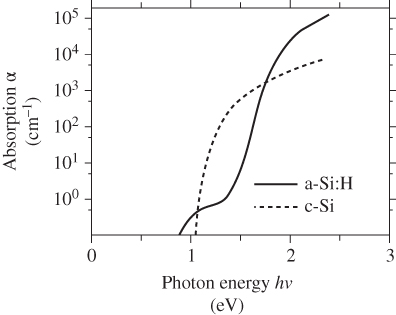
Figure 5.27 Absorption edge of amorphous silicon compared to crystalline silicon. There is about a half electronvolt energy difference in absorption edge between the two materials.
Source: Luque and Hegedus (2003). Copyright 2003. Reprinted with permission from John Wiley & Sons
Interesting features of the energy band diagram for amorphous silicon are shown in Figure 5.28. Owing to long‐range disorder the values of conduction band edge E c and valence band edge E v are not clearly defined as in crystalline silicon. This occurs because small variations in bonding energy exist for different bond angles and configurations associated with the structure in Figure 5.26. Density of states functions exist both for electrons below E c and for holes above E v that exponentially decrease in density into the energy gap. These are called bandtails. The bandgap is therefore not precisely defined, but may be approximated as in Figure 5.28 to be about 1.75 eV, although it does depend upon the preparation conditions of the material. There is an important distinction between states in bandtails within the bandgap and states outside the bandgap: the former are localised whereas the latter are delocalised. In ideal crystalline semiconductor material, all the band states are delocalised. Bandtails arise from localised disorder, which results in localised states. Conduction in a‐Si:H is essentially due to the delocalised states outside the bandgap.
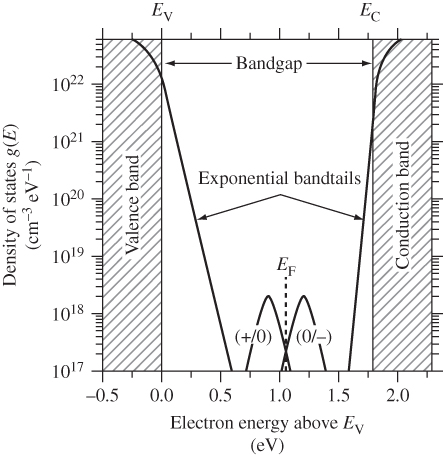
Figure 5.28 Density of electron states in a‐Si:H. Note the bandtails as well as the mid‐gap states due to defects.
Source: Luque and Hegedus (2003). Copyright 2003. Reprinted with permission from John Wiley & Sons
There are also states closer to mid‐gap. These are states that arise due to defects such as dangling silicon bonds. Dangling bonds were discussed in the context of surfaces and interfaces in Chapter 2, but they can also exist in a‐Si:H throughout the semiconductor. The density of these defects is strongly related to the degree of hydrogen termination of dangling bonds. As‐prepared material may have a low defect density below 1016 cm−3. Unfortunately, extended exposure to sunlight is well known to increase the defect density to about 1017 cm−3, which degrades the performance of solar cells over time until the new, higher defect density is stabilised. This process is known as the Staebler–Wronski effect, and is explained by the rearrangement of hydrogen atoms within the a‐Si:H.
Doping in a‐Si:H may be achieved by the incorporation of impurities such as phosphorus and boron as in crystalline silicon. In n‐type a:Si:H the measured free electron concentration is much smaller than the P‐doping level. This may be explained because a significant fraction of doped P atoms will occupy sites that are only bonded to three nearest silicon neighbours and the extra two P valence electrons remain in pairs tightly attached to the P atom. This does not lead to an additional localised shallow electron state and therefore does not result in n‐type doping. Occasionally, however, the P atom occupies a site that is bonded to four nearest silicon neighbours and n‐type doping is achieved.
Since there is a relatively high density of electron pairs bound to inactive P atoms in n‐type a‐Si:H, this material does not allow for effective hole transport because holes are trapped by these electron pairs. This puts constraints on the design and structure of an effective a‐Si:H solar cell.
The best structure for an amorphous silicon solar cell is suitably named the p–i–n structure. This is a p–n diode with a thick intrinsic layer sandwiched between thin p‐ and n‐layers. Typical devices have ≅20 nm thick p‐ and n‐layers and an intrinsic layer approximately 500nm in thickness. The reason for the insertion of the intrinsic layer relates to the problem of achieving both adequate hole and electron mobility in doped a‐Si:H material. The goal is to ensure that virtually all the photon absorption occurs in the intrinsic layer. This is in contrast to the crystalline solar cell, in which most absorption occurs in doped material. Mobilities of approximately 1 cm2 V−1 s−1 are typical in the intrinsic layer. This mobility value is small compared to crystalline silicon carrier mobility of the order of magnitude 1000 cm2 V−1 s−1; however, the typical thickness of amorphous solar cells of 0.5 μm is much thinner than a typical crystalline cell thickness of over 100 μm. This allows relatively small mobilities to be adequate.
The intrinsic layer in the thin‐film solar cell effectively establishes the width of the depletion region in the cell. The built‐in electric field is established across this intrinsic layer, and a key requirement is that carriers optically generated in this layer should reach the appropriate n‐ and p‐layers before recombining. The magnitude of this built‐in field can be estimated as follows: a 500 nm layer in a built‐in potential of 0.5 V results in an electric field of 104 V cm−1. Using ν = με and taking μ = 1 cm2 V−1 s−1 and ε = 104 V cm−1 we obtain ν = 104 cm s−1. If the intrinsic layer is L = 5 × 10⁻⁵ cm in thickness the carrier transit time to cross over the intrinsic layer becomes L/ν = 5 ns, and is clear that carrier lifetimes in amorphous silicon can be much shorter than carrier lifetimes in the microsecond range required for crystalline silicon solar cells.
The open‐circuit voltage of amorphous silicon cells is higher than in crystalline cells by about half a volt. This is explained by the increase in the absorption edge by a corresponding 0.5 eV in Figure 5.27. Typical measured open‐circuit voltages are close to 1 V.
There are two basic a‐Si:H device designs in which illumination is either incident through the substrate onto the lower surface of the cell or directly incident onto the upper surface of the cell.
In the transparent substrate design, a glass substrate is used and is coated first with a transparent electrode composed of a transparent conductive oxide (TCO) material such as tin‐doped In2O3 (ITO) or aluminium‐doped ZnO followed by the p‐type layer, which acts as a window, the intrinsic layer, the n‐type layer, and finally a rear electrode. It is usual for this rear electrode to be reflective since it allows light that was not absorbed to reflect back and once again have an opportunity to be absorbed. This design lends itself to low‐cost rigid solar panels. In the direct illumination design, the substrate may be non‐transparent. A practical material is a thin stainless‐steel sheet, which serves as the rear electrode and yields a flexible solar cell. The deposition sequence includes an n‐type layer, the intrinsic layer, and then the p‐type layer followed by a transparent front electrode. This type of design features bendability and low weight. See Figure 5.29.

Figure 5.29 Structures of a‐Si:H solar cells (not to scale). (a) Glass substrate structure with illumination through the substrate. (b) Stainless‐steel substrate structure with direct illumination. TCO, transparent conductor layer
An opportunity exists to further increase the percentage of light absorbed in the structures of Figure 5.29. This is accomplished using back reflectors that are not planar, but light scattering instead. Light that has traversed the active layers once has a high chance to reflect off the back reflector and back into the active layers at high angles relative to the thin‐film normal axis, which means that the optical path length through the active intrinsic layer is higher. In addition, light that has made a round trip and reaches the front electrode may exceed the critical angle and again reflect by total internal reflection and remain trapped inside the solar cell. Texturing of reflectors and TCO (transparent conducting) layers is used to maximise conversion efficiency in commercial devices.
The commercially achievable conversion efficiency of single‐junction a‐Si:H solar cells is approximately 7% for un‐aged devices and approximately 5% after 1000 h of exposure to sunshine, which allows the Staebler–Wronski degradation to stabilise. This is three to five times lower than crystalline silicon solar cell efficiency values. The application of single‐junction amorphous silicon solar cells is therefore limited to applications where low power and low cost are needed.
To increase the conversion efficiency of a‐Si:H solar cells, the most effective approach is to form a multiple junction device. Two or more thin‐film p–i–n junctions are stacked and effectively connected in series. Light that is not absorbed in the first junction passes to the second junction, and to subsequent junctions if present. The total voltage becomes the sum of the open‐circuit voltages from each p–i–n junction.
The key to success is to change the energy gap of each junction such that the first junction has the highest energy gap, which absorbs high‐energy photons but transmits lower energy photons to subsequent junctions that have decreasing energy gaps. In this scheme the open‐circuit voltage of the first p–i–n junction is highest, and takes better advantage of the higher energy photons, whereas in a single‐junction solar cell with a smaller bandgap these high‐energy photons generate EHPs that lose their excess energy in the form of heat before they get collected. This concept is known as spectrum splitting.
Tandem cells have two p–i–n junctions, and triple‐junction cells have three p–i–n junctions. The maximum amount of energy available increases with the number of cells in the stack since carrier energy loss through thermalisation decreases as the number of junctions increases. The optimum energy gaps required depend on the solar spectrum. For tandem cells an optimised stack included a first gap of ≅1.8 eV and a second gap of ≅1.2 eV.
There are other benefits that arise through the use of multiple junction cells. Total current for a given electrical output power decreases due to the higher output voltage. This decreases resistive losses. Also the thickness of each junction is less than for a single‐junction device. This lowers carrier recombination losses and effectively increases the fill factor of the overall device.
In order to achieve the required bandgap adjustments, Si must be combined with other elements during the formation of the amorphous layers. The best understood alloy is a‐Si1−x Ge x :H. By changing the value of x the bandgap may be adjusted from 1.1 eV (x = 1) to 1.7 eV (x = 0). This would appear to be an almost ideal way to prepare a tandem device; however, there are challenges. Germanium is much more expensive than silicon, and more importantly the effective defect density in a p–n junction increases as x increases, which lowers the fill factor of these p–n junctions. The defects trap carriers (holes in particular) in the intrinsic layer preventing them from being collected. In practice the minimum achievable bandgap is 1.4 eV.
One interesting way to reduce this problem is to vary the germanium concentration as a function of depth within the intrinsic layer of a given p–n junction. If the germanium content is raised towards the p‐side of the junction then holes photogenerated in the i‐layer will have a shorter distance to travel to the p‐side, effectively decreasing their chance of being trapped.
An effective triple‐junction amorphous cell has the structure a‐Si(1.8 eV)/a‐SiGe(≅1.6 eV)/a‐SiGe(≅1.4 eV), and after stabilisation over 10% efficiency is commonly achieved. To reach these efficiency values the operating points shown in Figure 5.9 must be matched in all three junctions. Specifically I MP for each junction must be the same under normal sunlight conditions. This requires careful optimisation of the thicknesses of each p–i–n junction. Back reflectors are incorporated, which influence the optimum layer thicknesses of each junction.
A key requirement for the successful operation of multiple junction solar cells is adequate conduction between each junction in the stack. In Figure 5.30 the structure of a tandem cell is shown. The n–p junction formed between the two p–i–n junctions is reverse‐biased during normal operation; however, it does allow current to flow because it operates as described for a tunnel diode in Figure 3.22. Tunnelling current can flow, provided degenerate doping levels are applied to both the n‐ and p‐layers, and these layers are therefore very heavily doped. Fortunately, this does not compromise the operation of the p–i–n devices since the critical light‐absorbing layer is the intrinsic layer.
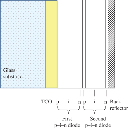
Figure 5.30 Tandem solar cell structure on glass substrate. The n–p junction formed at the interface between the first and second p–i–n diodes must be an effective tunnelling junction to allow carriers to flow to the next diode. The bandgap of the first p–i–n diode is higher than the bandgap of the second p–i–n diode. Similar tandem and triple‐junction structures may be formed on stainless‐steel substrates. TCO is a transparent conductive oxide layer
There is also a development in silicon thin‐film multiple junction solar cells in which one back layer of silicon is crystallised and is referred to as polycrystalline or microcrystalline rather than amorphous. These cells may be grown on glass substrates and crystallisation is achieved by rapid thermal annealing. The polycrystalline silicon layer has an absorption edge that is lower in energy allowing better utilisation of long wavelengths. However, the challenges are the following:
- Owing to the smaller absorption coefficient of crystalline silicon the recycling of light is critical, and highly reflective electrodes and light‐trapping schemes are essential.
- The polycrystalline silicon presents a large number of grain boundaries that act as recombination centres. The density of these grain boundaries can be decreased by increasing the silicon grain size, and grains of several microns are achievable. Increasing the grain size requires novel growth methods to avoid processing temperatures that exceed the glass softening temperature. Rapid thermal annealing may be performed using laser recrystallisation, in which rapid heating of the silicon without melting the glass substrate is possible. In addition, a suitable grain boundary surface treatment must be performed to minimise grain boundary surface recombination velocity.
Silicon tandem solar cells based on amorphous silicon as well as microcrystalline silicon yield approximately 10% conversion efficiency in production. See Problem 5.10.
5.14 Telluride/Selenide/Sulphide Thin‐Film Solar Cells
The best‐known large‐area thin‐film solar cells for power generation are not silicon‐based. Instead, the group II–VI semiconductor CdTe has been successfully developed and commercialised, and thin‐film cells with over 17% conversion efficiency are in large‐scale production.
CdTe may be grown either n‐type or p‐type. One method of achieving n‐type CdTe is to introduce excess Cd, whereas for p‐type CdTe excess Te is used. Dopants such as In and Au can also be used to achieve n‐type and p‐type doping, respectively; however, solar cells based on n‐type and p‐type CdTe have not demonstrated the highest solar cell efficiencies. A large number of heterojunction CdTe‐based solar cells have been investigated and p‐type single‐crystal CdTe in conjunction with n‐type In2O3:Sn, ZnO, SnO2, or CdS have been extensively investigated. The most effective thin‐film device is experimentally found to employ the p‐CdTe/n‐CdS structure. The thin‐film format gives CdTe solar cells the opportunity to be low in cost.
CdTe is a direct‐gap semiconductor with a bandgap of approximately 1.5 eV. Since it is a direct‐gap material it has a high optical absorption coefficient of 5 × 105 cm−1 for photons with energy greater than 1.5 eV. See its band diagram in Figure 2.17f and its absorption curve in Figure 5.5. Electron mobility in CdTe is 1000 – 1200 cm2 V−1s−1 and hole mobility is 50–100 cm2 V−1s−1 .
The form of these semiconductors used in thin‐film devices is polycrystalline. For CdTe cells, a thin film of p‐type CdTe of about 5 μm in thickness is grown and it absorbs sunlight to generate minority electrons. The film is composed of a large number of columnar single‐crystal grains. The size of a grain is typically in the range of 1.0 μm in cross‐section, and grain height is similar to the film thickness. In addition to the p‐type CdTe layer, there are other thinner layers in CdTe solar cells including the n‐type CdS layer and a TCO layer. CdS has a wider bandgap than CdTe and therefore acts simultaneously as a window material that offers minimal light absorption and as the n‐side of the p–n junction. A band diagram of the heterojunction is shown in Figures 5.31 and 5.32 show the device structure and morphology.

Figure 5.31 Band diagram of CdTe/CdS heterojunction. Note that the CdS is n‐type while the CdTe is p‐type. Since minority carriers are virtually all collected from the CdTe side as conduction band electrons, the large valence band offset does not play a significant role.
Source: Data from Kumar and Rao (2014)

Figure 5.32 Grain structure of CdTe solar cell also showing the CdS layer and device structure. TCO, transparent conductor oxide layer. The term ‘superstrate’ is used since the glass faces the incoming sunlight.
Source: Luque and Hegedus (2003). Copyright 2003. Reprinted with permission from John Wiley & Sons
Grain boundaries in the polycrystalline CdTe layer lower the minority carrier electron lifetime; however, since the layer is only approximately 5 μm thick, this is acceptable. Doping is challenging in CdTe because of complexes that form between dopants and vacancies, which tend to cancel the effect of doping. For example, Cl is expected to replace Te as a donor dopant; however, a chlorine ion has a high probability of forming a complex with a Cd vacancy. This Cl/Cd vacancy complex acts as an acceptor rather than a donor. This is an example of a self‐compensation mechanism. As a result, only approximately 1015 cm−3 n‐type doping in CdTe is achievable. In commercial devices, p‐type CdTe is employed to take advantage of the high mobility of minority electrons in this material.
The rear ohmic contact to the CdTe layer is problematic due to the doping self‐compensation effect. Copper‐doped ZnTe was used as a back contact for early CdTe solar cells but was abandoned due to copper's tendency to diffuse into the CdS layer. Copper is notorious for diffusion in a wide range of electronic applications due to its mixed valence states of +1 and +2, which result in weak ionic bonding and high densities of vacancies. The copper‐free compound material Sb2Te3 with a molybdenum capping layer is now well known and has shown stable performance. Manufacturers avoid publishing details of their specific contact materials and production methods.
The most successful growth method for the low‐cost production of high‐efficiency CdTe solar cells is a form of vapour deposition in which bulk CdTe is heated to approximately 500 °C causing it to sublime. The vapours then condense onto the glass substrate.
There is considerable controversy surrounding the long‐term viability of CdTe solar cells. An increasing number of countries are restricting the use of Cd, which is toxic.
In spite of these challenges, thin‐film CdTe solar cells were the first technology to break the long‐standing cost barrier of US $1.00 W−1 in 2008–2009 and are currently the leading thin‐film solar cell technology. CdTe is feasible for large‐scale solar farms.
More recently, a cadmium‐free, selenide‐based semiconductor material has been developed and solar cells using this material are in production. The material is a solid solution of CuInSe2 (CIS) and CuGaSe2 (CGS) that forms Cu(In x Ga1−x )Se2 (CIGS). The bandgap of CIGS varies continuously with x from about 1.0 eV for x = 1 to about 1.7 eV for x = 0.
CIGS is yielding thin‐film solar cells with 22% conversion efficiency in the lab and 15% in production as of 2017. The valence states of the elements are +1 (Cu), +3 (In, Ga), and −2 (S). CIGS has a very high optical absorption coefficient of more than 105 cm−1 for photon energies of 1.5 eV and higher, allowing layer thicknesses of only 1–3 μm to be sufficient for solar absorption.
As with CdTe solar cells, CIGS solar cells use a heterojunction with p‐type CIGS and a wide bandgap n‐type layer. The band diagram for a typical CIGS solar cell is illustrated in Figure 5.33. Note that CdS is shown as the n‐type layer; however, cadmium‐free substitutes for the CdS layer such as zinc oxysulphide, zinc magnesium oxide, and/or proprietary materials are also used to enable completely cadmium‐free CIGS solar cells. Figure 5.34 shows the cross‐section of a fabricated CIGS solar cell.
As of 2017, crystalline silicon solar cell costs have dropped dramatically, allowing crystalline and multicrystalline silicon solar cells to dominate the overall solar cell market. Silicon solar cell costs are at approximately US $0.30 W−1 putting intense pressure on all thin‐film technologies.
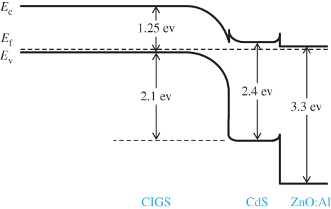
Figure 5.33 Band diagram of basic CIGS cell with a CdS n‐type layer. Alternative materials for the CdS layer are used in CIGS solar cells currently in production yielding Cd‐free CIGS thin‐film solar cells.
Source: Data from Płaczek‐Popko (2017)
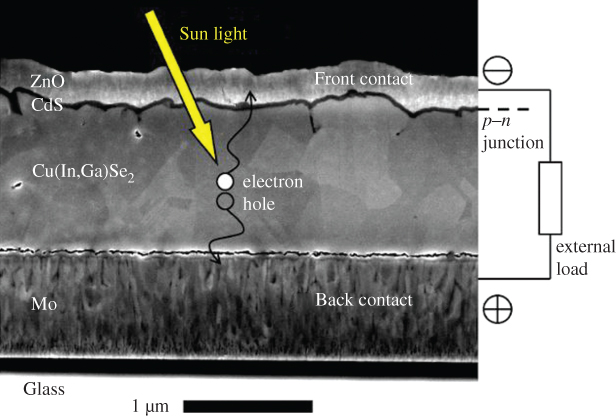
Figure 5.34 Scanning electron microscope cross‐section of a CIGS solar cell. Note that unlike CdTe thin‐film cells, the glass substrate is at the rear of the cell and light enters through the ZnO transparent front electrode.
Courtesy of D. Abou‐Ras, Helmholtz‐Zentrum Berlin.
5.15 High‐efficiency Multi‐junction Solar Cells
An important area of active development of solar cells involves increasing efficiency. The motivation for this comes from several factors. For space applications, weight is crucial. For terrestrial applications, the opportunity to concentrate sunlight onto smaller solar cells is attractive (see Section 5.16). A premium price per watt can therefore be charged for higher efficiency solar cells. In addition, cost reductions in substrate and packaging materials and transportation and installation are attractive motivators.
The achievement of 30–40% conversion efficiency in single‐crystal multi‐junction solar cells has been an important milestone in solar cell development (Figure 5.19) and the single junction Shockley–Queisser limit can be exceeded. In addition to space applications, these high‐efficiency cells are also useful in spite of their high cost for terrestrial concentrating solar cell installations in which sunlight is concentrated using mirrors or lenses to yield more power per unit area of solar cell. Concentration factors of several hundred are achievable, although tracking or angular movement of the solar cell is required to follow the sun's position. See Section 5.16.
The best‐known tandem single‐crystal solar cell uses germanium as a substrate. Germanium has a convenient lattice constant since it almost perfectly matches the lattice constant of GaAs. See Figure 2.34c. In addition, Ge has a small bandgap allowing it to absorb longer wavelengths of light than silicon. By growing thin‐film epitaxial layers of III–V semiconductors on the Ge substrate, a tandem cell with two or three junctions can be formed that absorbs effectively over a wide wavelength range of solar radiation.
The structure of a triple‐junction solar cell is shown in Figure 5.35. The GaAs thin‐film cell is epitaxially grown on the Ge substrate. A third semiconductor, Ga1−x In x P, is grown epitaxially on the GaAs. From Figure 2.34a it can be appreciated that the lattice constant of Ga1−x In x P can be set to match GaAs provided the appropriate value of x is chosen. This value of x is close to 0.5 and the resulting bandgap is about 1.95 eV. The triple‐junction solar cell therefore has three bandgaps of approximately 0.7 eV (Ge), 1.43 eV(GaAs), and 1.95 eV(Ga1−x In x P). A useful way to visualise the principle behind multi‐junction solar cells is shown in Figure 5.36. Current flow through each cell is the same due to the series connection between cells. Therefore current matching between cells is critical to prevent a weak link in the series connection of cells. This places constraints on the bandgaps of the cells in the stack which are further optimized compared to those in Figure 5.35.

Figure 5.35 Structure of triple‐junction solar cell showing germanium wafer upon which two larger bandgap semiconductors are deposited epitaxially. The total output voltage is obtained between the metal grid and the rear electrode

Figure 5.36 Multi‐junction solar cell showing the portions of the spectrum that are covered by each material. Note that the infrared wavelengths above 2000 nm are not absorbed. The GaAs junction is modified and further optimised by the addition of a small indium component. Note that the three cell voltages add together; however, the cell current is controlled by the minimum current that is supplied by each of the cells. This means that current matching between the multiple cells in a multi‐junction cell is important.
Source: Yastrebova (2007)
Reversed p–n junctions exist between each solar cell p–n junction in the tandem cell. These reversed junctions are shown as tunnel junctions in Figures 5.35 and 5.36. Tunnelling allows effective current flow with minimal voltage drop from one cell to the next. A band diagram showing a tunnelling junction situated between two p–n junctions is shown in Figure 5.37.

Figure 5.37 Tunnelling between the InGaP and GaAs cells in a tandem solar cell shown in a band diagram.
Source: Wikimedia Commons
Applications of crystalline high‐efficiency tandem cells are limited to niche markets including space, avionics and concentrator systems due to their high cost.
The use of germanium wafers is not cost‐effective for non‐concentrating terrestrial applications. The multi‐junction solar cell is an area of active development driven by the promise of still higher efficiencies and lower production cost per watt. Theoretical models show that efficiencies of over 60% are possible in a multi‐junction cell provided the number of junctions is increased to five or more junctions in tandem. The desire exists eventually to achieve cost‐effective high‐efficiency multi‐junction solar cells for terrestrial use without the need for optical concentration, but currently the high materials and fabrication costs far outweigh the improvement is efficiency compared to single‐junction solar cells.
One approach under development for tandem solar cells is the use of a graded composition strain‐accommodation layer. For example, a 4% lattice mismatch between silicon and germanium causes a high density of dislocations if germanium is grown directly on silicon substrates; however, dislocations can be minimised by growing a layer of Si x Ge1−x. The graded layer is initially silicon‐rich to accommodate to the silicon substrate, and as growth proceeds, the germanium concentration increases. Dislocation densities low enough for high performance solar cells are achievable. Graded layers in III–V semiconductors are also possible allowing for changes in lattice constant between successive cells having different bandgaps to be possible. The additional cost of growing graded layers is a challenge for solar cell applications, which are almost always very cost‐sensitive.
Direct‐gap III–V semiconductors can replace germanium substrates in tandem solar cells. Double‐, triple‐, or quadruple‐junction tandem cells using GaAs and InP substrates may be fabricated even in the absence of lattice matching between all the layers. A technique known as wafer bonding may be employed to achieve the required tunnelling junctions between cells even if the lattice constants of the semiconductors used for successive cells change. During fabrication a first solar cell p–n junction having a first lattice constant may be epitaxially grown on a first substrate. A second solar cell grown on a second substrate having a second lattice constant may also be epitaxially grown. Next the two cells may be bonded together face‐to‐face by applying heat and pressure. Chemical bonds are formed between the two lattice‐mismatched layers. Extreme care to maintain cleanliness, flatness, and smoothness is essential for wafer bonding to be successful. Finally, the substrate of one of the bonded cells may be removed by polishing and/or etching.
The wafer bonding technique adds costs. It is a widely used process for light emitting diode (LED) fabrication and will be further discussed in Chapter 6 where the costs can be justified; however, for solar cells it is not currently economical for mass production. See Problem 5.19.
5.16 Concentrating Solar Systems
Concentrator solar technology concentrates sunlight onto solar cells using either reflective optics in the form of curved mirrors, or refractive optics in the form of traditional lenses or Fresnel lenses. Concentration of sunlight intensity by factors of hundreds or even a thousand are possible. This approach can reduce the size requirements of solar cells and is even more attractive since the Shockley–Queisser limit is higher for concentrated sunlight as shown in Figure 5.18. Nevertheless, concentrating solar systems suffer from several difficulties:
- The optical system must be aimed at the sun to maintain maximum solar power on the solar cell at all times of the day and over all seasons. This requires tracking devices that move the optical system mechanically. Single‐axis trackers only move in one axis and can follow the sun over the course of one day; however, it is more optimal to use dual‐axis tracking to allow for seasonal variations of sunlight. The higher the solar cell gain, the more precise the tracking needs to be since the focus of the sunlight will fall onto a smaller area.
- The high intensity will cause a temperature increase at the solar cell due to light that is absorbed but does not directly contribute to electrical power. Since even the best commercial multi‐junction solar cells have efficiency values of under 40%, more heat energy than electrical energy is produced and cooling is generally required. For high concentration factors of several hundred, liquid cooling may be used. Cooling systems add to system cost, although thermal storage of heated liquids is possible as a secondary source of energy.
- The efficiency of crystalline silicon solar cells decreases as temperature rises, which will offset some of the benefits of solar concentration including the efficiency gain noted in Figure 5.18 (see Example 5.2 and Problem 5.7). This, although not as significant as in silicon, is also an issue for wider bandgap III–V semiconductor solar cells and multi‐junction cells.
- In the case of high solar concentrations, the resulting minority carrier density can be high enough for Auger recombination to occur. In this process, high concentrations of EHPs suffer increasingly high probabilities of recombination, thereby reducing minority carrier lifetime. Auger recombination involves energy exchange between two electrons that enables energy released due to the recombination of a first electron with a hole to excite a second electron into a higher energy state within a band. The relaxation of this second electron occurs by thermalisation and no solar cell current flow occurs from the initial EHP. See Figure 5.38. Auger recombination is also an important issue in LEDs and will be further discussed in Chapter 6.
- On cloudy days, non‐concentrating solar cells will still generate a sizeable fraction of their power output; however, concentrator systems will not function well due to the diffuse sunlight, which cannot be focused.
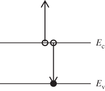
Figure 5.38 Auger recombination process. Two electrons are involved. A first electron recombines with a hole but instead of producing a photon, energy is conserved by a second electron that is excited high up into the conduction band. This second electron then thermalises rapidly and heat is produced. Indirect‐gap transitions can also occur since the second electron can undergo a momentum change that allows for overall momentum conservation
For these reasons the deployment of concentrating solar cell installations is not very popular. Concentrator‐based solar farms do exist but they are not currently cost‐competitive compared to non‐tracking installations. Some of these aspects are further explored in Problem 5.8.
5.17 Summary
- A solar cell consists of a p–n junction in which sunlight generates electron–hole pairs that are collected by the external circuit and provide electrical power. Carrier flow occurs by drift across the depletion region in the solar cell and operation is in the fourth quadrant of an I–V diagram. The potential barrier in a solar cell p–n junction at the operating point should be as small as possible to maximise the output voltage of a solar cell, but must be large enough to maintain a suitable reverse current.
- Light absorption in a solar cell is sensitive to the type of bandgap. Indirect‐gap semiconductors have weaker absorption than direct‐gap semiconductors over a range of photon energies. The absorption in indirect‐gap material requires the participation of phonons and thicker cells are required.
- The solar spectrum is based on the blackbody radiation spectrum at a temperature corresponding to the surface of the sun at 5250 °C. This spectrum is affected by atmospheric absorption due principally to oxygen, water vapour, and carbon dioxide.
- A crystalline silicon solar cell consists of a thin n‐type front layer and a thick p‐type layer. A front electrode metal grid, back‐contact metallisation, and an anti‐reflection layer complete the device. Sunlight that is absorbed within the depletion region or within a diffusion length on either side of the depletion region has the best chance of generating power in an external circuit. Short‐circuit current, open‐circuit voltage, and fill factor are useful characterisation parameters.
- In ‘thin’ solar cells diffusion lengths exceed the thickness of the cell. Surface recombination velocity is an important parameter that allows us to quantify the chances of carriers recombining at surfaces instead of through the external circuit. Methods to minimise surface recombination velocity include a back surface field and oxide‐layer passivation.
- The generation of usable current as a function of depth in a solar cell may be determined by assuming that light is absorbed at a specific depth and then determining the collection of holes and electrons from this depth. The total resulting current due to generation from all depths may be calculated by superposition.
- The limiting solar cell efficiency is dependent on the bandgap of the solar cell. Limitations in efficiency arise from photons that are too low in energy to be absorbed or photons with too much energy that must thermalise before they can be collected. In addition, the operating voltage is lower than the bandgap energy, which represents a further energy loss. Silicon has achieved a conversion efficiency of approximately 25%. Maximum efficiencies are predicted by the Shockley–Queisser limit.
- Silicon for silicon solar cells starts with metallurgical grade material that is most commonly refined using the Siemens process. The resulting solar‐grade materials may be cast into multicrystalline ingots or grown into boules by the Czochralski method. Wire sawing is used to cut wafers. Single‐crystal silicon is a few percent more efficient that multicrystalline silicon.
- Solar cell wafer processing includes texturing, back and front surface doping and contacting, and the deposition of an anti‐reflection layer. Screen printing offers a low‐cost approach to processing.
- Silicon ribbon technology is an alternative to wafer dicing for solar cells. Silicon is pulled directly from the melt as a liquid held between two wires by surface tension.
- Thin‐film silicon amorphous solar cells use a random silicon structure with no long‐range order but predominantly tetrahedral bonding. Dangling bonds are terminated by hydrogen. The bandgap of amorphous silicon is about 1.75 eV and it behaves more like a direct‐gap semiconductor. The p–i–n structure is used to fabricate solar cells due to short carrier lifetimes in doped material. Tandem and triple‐junction designs can increase conversion efficiency up to approximately 10%.
- Thin‐film solar cells based on CdTe and CIGS achieve over 15% efficiency without the need for multi‐junction architectures. Both CdTe and CIGS are direct‐gap semiconductors. CdTe solar cells were the first to break the US $1 W−1 cost barrier. CIGS cells can be designed to eliminate the use of cadmium.
- Multi‐junction solar cells have achieved over 30% conversion efficiency. The best‐known devices are grown by epitaxial layer growth of III–V semiconductors lattice matched to a germanium substrate. The solar spectrum is more efficiently utilised than in single‐junction solar cells and the maximum theoretical efficiency is above 60%. Wafer bonding or graded composition strain‐accommodation layers can be used to allow for changes in lattice parameter.
- Concentrating solar systems allow for sunlight to be concentrated onto smaller, high‐efficiency solar cells. This can help to justify the cost of multi‐junction solar cells; however, tracking systems are required to maintain optimum system efficiency, and sunlight diffused by clouds does not concentrate effectively.
References
- Green, M.A. (1981). Solar Cells. New Jersey: Prentice Hall. pp. 128, 130, 189. ISBN 0‐85823‐580‐3.
- Kumar, S.G. and Rao, K.S.R. (2014). Physics and chemistry of CdTe/CdS thin‐film heterojunction photovoltaic devices: fundamental and critical aspects. Energy & Environmental Science 7: 45–102.
- Luque, A. and Hegedus, S. (2003). Handbook of Photovoltaic Science and Engineering. John Wiley & Sons. ISBN: 978‐0‐471‐49196‐5.
- Płaczek‐Popko, E. (2017). Fabrication of CdMgTe/Cd(Mn)Te nanostructures with the application of high‐resolution electron‐beam lithography. Opto‐Electronics Review 25 (2): 55–64.
- Shockley, W. and Queisser, H.J. (1961). Detailed balance limit of efficiency of p–n junction solar cells. Journal of Applied Physics 32: 510.
- Sze, S.M. (1985). Semiconductor Devices: Physics and Technology. New York: John Wiley & Sons. ISBN: 9780471837046.
- Yastrebova, N.V. (2007). High‐Efficiency Multi‐Junction Solar Cells: Current Status and Future Potential. Wikimedia Commons.
Further Reading
- Green, M.A. (1992). Solar Cells, Operating Principles, Technology and System Applications. University of New South Wales.
- Luque, A. and Hegedus, S. (ed.) (2003). Handbook of Photovoltaic Science and Engineering. Wiley.
- Streetman, B.G. and Banerjee, S.K. (2006). Solid State Electronic Devices, 6e. Prentice Hall.
Problems
-
5.1 Write a short two‐to‐three‐page qualitative description in your own words of the processes involved in producing electric power from a p–n junction solar cell. Include diagrams as necessary. You should refer specifically to the following:
Optical absorption
EHP production
Carrier drift/diffusion
Recombination
Diffusion length
Open‐circuit voltage
Short‐circuit current
-
5.2 Solar radiation is fundamentally determined by blackbody radiation. Blackbody radiation produces a radiation spectrum described by Planck's law. Planck's law describes the radiance as a function of frequency ν of electromagnetic radiation emitted from a non‐reflective surface of a body in thermodynamic equilibrium at temperature T. As a function of ν in cycles per second and T in kelvins, Planck's law is

and represents the emitted power in watts per unit area of an emitting surface at temperature T per unit solid angle per unit frequency. It provides what is referred to as a specific radiative intensity.
- Using a computer, plot I (ν, T) as a function of ν on a single set of coordinates for the following temperatures: T = 1500 K, T = 2500 K, T = 3500 K, T = 4500 K, and T = 5500 K. For each plot, estimate the perceived colour of the observed emission and find the wavelength at which I (ν) is a maximum. At what wavelength is sunlight a maximum?
- For each temperature, find the fraction of total radiated power that falls in the visible light range between 400 and 700 nm. Hint: Use the area under the curve of I (ν, T).
- The CIE diagram of Figure 4.14 shows the locus of colour coordinates x and y due to blackbody radiation. Show the point on this locus corresponding to a tungsten filament lamp operating at 3500 K. How much below the melting point of tungsten is this? Also show the point on the locus corresponding to the light emitted by the sun.
-
5.3 Anti‐reflection layers applied to silicon solar cells function in a manner similar to those used on camera lenses and eyeglass lenses. If light is incident normal to a first interface between two transparent optical media with different indices of refraction, reflection will take place. If the reflection at a second interface is arranged to cancel out the first reflection by ensuring that both the magnitude and the phase of the reflections will cancel out the first reflection, then overall reflection is reduced or eliminated. The reflection coefficient R is
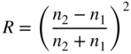
A simple example of this is the interface between air and glass shown below:
Air has index of refraction n 1 ≅ 1.0 and glass has index of refraction n 2 ≅ 1.5. Therefore,
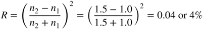
Note that the same reflectivity is obtained from the air–glass interface whether the light is incident from air onto the air–glass interface or from the glass onto the glass–air interface.
An anti‐reflection layer having index of refraction n 2 as shown below creates two interfaces, one between media 1 and 2, and one between media 2 and 3:
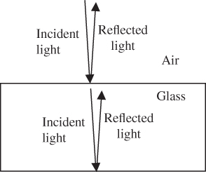
-
Regard n
1 and n
3 as given, but n
2 as an adjustable parameter. Find the value of n
2 in terms of n
1 and n
3 that will cause the reflection from the interface between 1 and 2 to be the same in magnitude as the reflection from the interface between 2 and 3.

- If medium 1 is air and medium 3 is glass, find the numerical value for n 2 that satisfies the criterion of (a).
-
In order for the reflections to cancel out, the phases of the light waves leaving the interfaces must also be arranged to be 180° out of phase with each other. Show that the smallest possible thickness δ of medium 2 is
 , where λ is the wavelength of the light in medium 2.
 - For the conditions in (b) find the smallest possible thickness of medium 2 to allow for cancellation of reflection for light having wavelength 600 nm. Hint: Wavelength in a medium having index of refraction n is reduced relative to its wavelength in vacuum by a factor of n.
- Assuming that silicon is a transparent medium, and using information in the appendices, find both the thickness and index of refraction of an anti‐reflection layer that could be deposited on silicon if it is situated in air.
- Tantalum oxide is a popular anti‐reflection material for silicon solar cells. Look up the refractive index of tantalum oxide and compare with your answer to (e).
- Since silicon solar cells are generally bonded to a glass front sheet with n ≅ 1.5, repeat steps (e) and (f) if the air is replaced with glass. In which case (air or glass) does tantalum oxide best match the calculated refractive index? You may neglect the front reflection off the glass sheet at the air interface.
- Compare the expected efficiency of a silicon solar cell with an anti‐reflection layer to that without an anti‐reflection layer. Hint: Light that is not reflected will be transmitted into the silicon. Assume a wavelength of 550 nm.
- Silicon solar cells with an anti‐reflection coating generally have a deep‐blue colour. Explain this based on your understanding of anti‐reflection layers.
-
Regard n
1 and n
3 as given, but n
2 as an adjustable parameter. Find the value of n
2 in terms of n
1 and n
3 that will cause the reflection from the interface between 1 and 2 to be the same in magnitude as the reflection from the interface between 2 and 3.
- 5.4 Show that Eq. 5.2 is the solution to Eq. 5.1 by substituting it into the differential equation. Also show that Eq. 5.3a is obtained from Eq. 5.2 by applying the appropriate boundary conditions.
-
5.5 Using the expressions for diffusion current,

and

show that Eqs. 5.4a and 5.4b are obtained from Eqs. 5.3a and 5.3b.
-
5.6 The optical generation rate inside a silicon solar cell at room temperature in a certain flux of sunlight is assumed to be a constant value G = 5 × 10¹⁹ EHP cm−3 s−1. If W = 1.0 μm, the electron and hole lifetimes are 2 × 10⁻⁶ s, I
0 = 1 × 10⁻⁹ A and the cell area is 100 cm2, calculate the following:
- The optically generated current I L.
- The short‐circuit current I SC.
- The open‐circuit voltage V OC.
- The maximum output power if the fill factor is 0.8.
-
5.7 A silicon solar cell of area 100 cm2 has doping of N
a = 5 × 1018 cm−3 and N
d = 5 × 1016 cm−3. If the carrier lifetimes are 5 × 10⁻⁶ s and the optical generation rate inside the silicon solar cell is assumed to be a constant value of G = 3 × 10¹⁹ EHP cm−3 s−1, calculate the following:
- The optically generated current I L. State and justify any assumptions you used to obtain your solution.
- The short‐circuit current I SC.
- The open‐circuit voltage V OC at room temperature.
- The open‐circuit voltage at 100 °C and at −50 °C.
- The maximum output power if the fill factor is 0.8 at both room temperature and at 100 °C.
- If G is increased by a factor of 100 by a solar concentration system to 3 × 10²¹ EHP cm−3 s−1, calculate the maximum power output. Confirm that it rises by more than a factor of 100, and state the assumptions you are making in this calculation.
-
5.8 Concentrating solar cells require an optical means of concentrating sunlight onto solar cells.
- Research concentrator solar cells and find three designs that have been used for concentration of sunlight. Explain their optical design using a diagram. You should make sure you have at least one reflective design and one refractive design, although there are designs that use both reflection and refraction.
- The concentrator designs allow for the use of high‐efficiency multi‐junction cells. If concentration by a factor of 200 is achievable and multi‐junction solar cells with efficiency of 30% are used in place of silicon cells having 15% efficiency, how many cloudy days per year would cancel out the benefit of the efficiency improvement in terms of energy produced over one year? Assume that a cloudy day reduces the power output from a non‐tracking cell by a factor of 3, and assume that the concentration factor is eliminated by the clouds. Make and justify any additional assumptions you use.
- Deserts are locations with little rainfall. Look up the average number of cloudy days per year present in major deserts and compare the results with your answer to (b).
- Look up the global total installed concentrator solar cell capacity relative to the non‐concentrated solar cell capacity and try to justify the lack of popularity of concentrator installations.
-
5.9 A solar panel consists of 80 circular, 15‐cm diameter silicon wafer‐based cells laminated onto a glass plate.
- Calculate the maximum power output from the panel. Assume that the silicon cells are 18% efficient.
- Sunlight, over the course of one day, is modelled as a light source that rises and sets and at noon the sunlight is incident normal to the cell, whereupon it provides 1000 W m−2 of optical power. Calculate the total energy output in units of watt‐hours over the course of one day. Make and justify any other assumptions needed.
- A typical family home is frequently assumed to require approximately 3000 W of solar panel capacity to satisfy its energy needs. Justify this based on your answer to (b) by considering the energy requirements of a home including heating, hot water, and lighting. How many solar panels would be required? Make a table to show energy consumption for a range of uses in kWh (kilowatt‐hours).
-
5.10 One thin‐film solar technology is based on amorphous/microcrystalline silicon. Efficiency levels of approximately 9% are achieved in production. A triple‐junction version of this architecture achieves a cell conversion efficiency ranging from 11 to 13%.
- Sketch your understanding of the device structure. What would you estimate the open‐circuit voltage to be?
- Look up the appropriate information on the web and summarise the performance values published in the literature. Recommended key words: triple‐junction thin‐film silicon, Sharp Corporation (Japan).
- What advantages does this technology have compared to CdTe thin‐film solar cells?
- What disadvantages does it have compared to CdTe thin‐film solar cells?
-
5.11 Cadmium telluride thin‐film solar cells require only 2% of the semiconductor content of crystalline silicon solar cells. Read the literature available from the thin‐film CdTe industry. Summarise the available modules and their efficiency and power output specifications. Recommended key words: First Solar Corporation (USA), CdTe thin‐film solar cells.
- How are toxicity and potential environmental issues addressed by the manufacturer?
- List and explain two other positive attributes of CdTe thin‐film solar panels as presented by CdTe PV manufacturers.
- The installation of solar farms is the biggest use of CdTe technology. Find the 10 largest solar farms globally in terms of peak power output and list the solar cell technology used for each farm. What percentage of these are CdTe‐based?
- The average output of these 10 largest solar farms may be exceeded by solar farms currently either under construction or planned for construction. Find information on these near‐term projects and repeat part (c) for these future farms.
-
5.12 The prospect exists for obtaining over 50% conversion efficiency in a multi‐junction solar cell with more than three solar cells in tandem. If both the II–VI and the III–V solar cell materials are used, a set of five junctions using direct‐gap semiconductors is available; see Figure 2.34c.
- Explain why an increasing number of junctions in tandem could, in principle, allow for a higher overall efficiency for a PV solar cell operating with illumination from the sun.
- Using Figure 2.34c describe the possible structure of a solar cell with five tandem junctions. What substrate could be used to provide a lattice constant suitable for all the layers? Is such a substrate available?
- 5.13 The single‐crystalline silicon solar cell may be further optimised by a back electrode structure in which both the anode and cathode contacts are attached to the rear of the cell in closely spaced stripes. This cell architecture has the advantage that the front of the silicon solar cell is completely available for sunlight absorption and no power is blocked by front electrodes. Since the electrodes are all on the back of the wafer, carriers must flow laterally inside the wafer and electrons and holes will drift to adjacent electrode stripes on the back of the wafer. The overall efficiency of these cells is a remarkable 24–25% in production quantities. Find additional information on this type of solar cell. Prepare a two‐to‐three‐page summary of the cell structure and the important distinctions between these rear electrode cells compared to the traditional front/rear electrode cells. Hint: Use the following search terms: SunPower rear electrode solar cell.
-
5.14 Derive Eqs. 5.16a and 5.16b using the appropriate boundary conditions.
-
Using the first three terms of Taylor series expansion
 … simplify Eqs. 5.16a and 5.16b. You may assume that the thicknesses of the n‐ and p‐sides are both much smaller than the diffusion lengths of holes and electrons, respectively. You should obtain Eqs. 5.17a and 5.17b.
 - Show that your resulting equations satisfy the required boundary conditions.
-
Using the first three terms of Taylor series expansion
-
5.15
- Derive Eqs. 5.18a and 5.18b using the appropriate boundary conditions.
-
Using the first one or two terms of Taylor series expansion
 … simplify Eqs. 5.18a and 5.18b. You may assume that the thicknesses of the n and p sides are both much smaller than the diffusion lengths of holes and electrons, respectively. You should obtain Eqs. 5.19a and 5.19b.
 - Show that your resulting equations satisfy the required boundary conditions.
- Plot Eqs. 5.18a and 5.18b for the following case: Silicon at room temperature, n p = 1000 cm−3 , p n = 100 cm−3 , x b = 100 μm, x s = 1 μm, and V = 0.6 V. Compare your plot to the shape of Figure 5.11 and explain. Assume τn = τp = 100 μs.
-
5.16
- Derive Eqs. 5.21a and 5.21b using the appropriate boundary conditions.
-
Using the first three terms of Taylor series expansion
 … simplify Eqs. 5.21a and 5.21b. You may assume that the thicknesses of the n‐ and p‐sides are both much smaller than the diffusion lengths of holes and electrons, respectively. You should obtain Eqs. 5.22a and 5.22b.
 - Show that your resulting equations satisfy the required boundary conditions.
-
5.17 Consider that electron–hole‐pair generation occurs at two depths in the p‐side of a silicon solar cell as illustrated in Figure 5.15. Assume the following parameters:
G 1 = 1022 EHP cm−3 s−1 and x 1 = 25 μm
G 2 = 6 × 10²¹ EHP cm−3 s−1 and x 2 = 125 μm
Assume that G 1 occurs over a depth range of 1 μm centred at 25 μm or from 24.5 to 25.5 μm. Assume G 2 occurs over a depth range of 1 μm centred at 125 μm or from 124.5 to125.5 μm. The generation depth range at each of x 1 and x 2 can be considered very small. This means that you can determine the total excess hole flux flowing away from depth x 1 by multiplying G 1 by 1 μm. The units will represent a flux density J 1 . The same approach is applicable at depth x 2 to obtain flux density J 2 .
Minority electron lifetime τ = 1 × 10⁻⁵ s. Assume an infinitely thick p‐region.
- Find the solar cell short‐circuit current density if only G 1 is present.
- Find the solar cell short‐circuit current density if only G 2 is present.
-
Assume that both
G
1
and
G
2
are simultaneously present. Solve the diffusion equation in three regions:
-

- x 1 ≤ x p ≤ x 2
- x p ≥ x 2
-
- Apply suitable boundary conditions to the results of (c). Sketch the excess minority carrier concentration as a function of x p.
- Using your results of (d) calculate the total solar cell current density.
Compare the result of (e) to the sum of the results of (a) and (b). Comment on your comparison as it pertains to superposition described in Section 5.7. Hint: Work out answers to (b), (d), and (e) using variables J 1 and J 2 first.
- 5.18 How could the superposition approach discussed in Section 5.7 be used to calculate the total current supplied by a conventional silicon solar cell? Think about the solar spectrum and the fact that the optical absorption coefficient of silicon is wavelength‐dependent.
- 5.19 Look up details on wafer bonding for tandem solar cells using the Internet. What substrates are used? Wafer bonding has enabled quadruple‐junction experimental tandem cells. Describe the sequence of layers and bandgaps as well as the resulting performance values of completed tandem solar cells.
-
5.20 Obtain a copy of the original paper presenting the Shockley–Queisser limit:
Shockley and Queisser (1961).
- Read the paper carefully.
- Write a well‐constructed summary of the physics used to obtain the results and the efficiency limiting aspects for each of the following:
- Spectral absorption losses
- Thermalisation losses
- Potential losses
- Thermodynamic limit.