
8
Junction Transistors
8.1 Introduction
The understanding we have now acquired of p–n junction diodes allows us to explain and model the first commercialised transistors, the bipolar junction transistor ( BJT ) developed in the 1950s at Bell Labs and the junction field‐effect transistor ( JFET ) developed about 10 years later. Both of these p–n junction–based transistors are still in use today.
8.2 Bipolar Junction Transistor
In Section 5.1, we explained the I–V curves for a p–n junction illuminated by a light source. Figure 5.2 as described by Eq. (5.7) shows how the reverse saturation current of a p–n junction is increased by the optical generation of minority carriers at or near the depletion region. Consider a reverse‐biased p–n junction with a power supply and a load resistor connected as shown in Figure 8.1.

Figure 8.1 Reverse‐biased p–n junction in series with a resistive load
If light shines on this junction, the reverse saturation current increases and the power flowing through the load increases. The magnitude of the reverse bias voltage across the diode is the supply voltage less the voltage across the resistor:
Figure 8.2 shows a load line based on resistor R. The voltage VR across the resistor can be varied by the intensity of the light and can range from almost zero if only the reverse saturation current flows through the diode (no illumination) to almost V S if illumination is strong enough. If we regard the resistor as a load, the photodiode becomes a way to control a voltage VR and a resulting current I = VR /R across the load.

Figure 8.2 Current‐voltage characteristics of photodiode connected to resistive load as in Figure 8.1
A transistor is a device that controls a voltage and a resulting current across a load in response to an electrical input rather than by using light intensity as an input. In order to achieve this, we can consider how to vary minority carrier concentration in a reverse‐biased diode in response to an electrical input voltage or current.
We will now show that a controllable concentration of minority holes can be electrically produced in the n‐type material of the reverse‐biased p–n junction. Since only one minority carrier type is required for reverse diode current to flow, it is acceptable to only generate holes. Later we will also show that minority electrons could also be electrically generated in the p‐type material of a reverse‐biased p–n junction.
In Chapter 3, we concluded that the p–n junction in forward bias causes minority carriers to be injected into both the p‐side and the n‐side of the junction. If one side of the junction has much higher doping than the other side, then most of the minority carrier injection and hence most of the overall current flow are attributable to only one minority carrier type.
We will now consider a p + –n junction. Since the p‐side is heavily doped, the equilibrium minority electron concentration n p in the p‐side will be small compared to the equilibrium minority carrier concentration p n in the n‐side. From Section 3.5, we see that minority carriers exist as excess holes in the n‐side of a p–n junction and from Eq. (3.21b) we obtain

The excess hole concentration δp(x n) is exponentially related to applied voltage V, and therefore, only a small change of V in forward bias across this p–n junction can lead to orders of magnitude of change in δp(x n). If these minority holes could somehow be made available to the reverse‐biased p–n junction of Figure 8.1, then we would have the ability to control the current flow through the reverse‐biased p–n junction by varying the voltage V across a forward‐biased p–n junction.
Since the excess minority holes in the n‐side of a forward‐biased p–n junction drop off exponentially with distance away from the edge of the depletion region, we could position the reverse‐biased p–n junction as closely as possible to the forward‐biased junction and preferably well within a diffusion length of the forward biased junction. The resulting device is shown in Figure 8.3 with a forward bias connected to a first junction and a reverse bias connected to a second junction. This is the structure of a BJT.

Figure 8.3 Voltages and currents in a PNP BJT
Since we produce excess holes in the n‐type region due to the p+–n junction, this p+ region is called the emitter. Since we remove the minority holes from the reverse‐biased junction using the p‐type material on the right side, we call this the collector. The n‐type region is called the base for historical reasons since the first BJT was mechanically supported by this n‐type layer.
The most important region to understand is the base of the transistor because holes injected from the emitter–base junction diffuse through the base and then drift across the base–collector junction into the collector.
We can establish a coordinate system as shown in Figure 8.4. Here the excess minority electron concentration in the base
δp
n(x
n) at the base–emitter depletion boundary is ![]() and in the base at the base–collector depletion boundary, it is
and in the base at the base–collector depletion boundary, it is ![]() .
.

Figure 8.4
Base region of width  is located between two depletion regions
We can now determine two boundary conditions relevant to the base region at x n = 0 and at x n = W b .
![]() is obtained from the excess carrier concentration that exists on the p‐side of the base–emitter p–n junction for a given base–emitter bias voltage. Using Eq. (3.21b) we obtain
is obtained from the excess carrier concentration that exists on the p‐side of the base–emitter p–n junction for a given base–emitter bias voltage. Using Eq. (3.21b) we obtain

where
V
BE
is the base–emitter voltage. If ![]() for a forward biased base–emitter junction, then we can write
for a forward biased base–emitter junction, then we can write

We can also determine ![]() by considering the base–collector p–n junction:
by considering the base–collector p–n junction:

where
V
CB
is the collector–base voltage. If ![]() for a reverse‐biased base–collector junction, then we can write
for a reverse‐biased base–collector junction, then we can write
Since p n is a very small number, we will approximate this to zero and hence,
The excess minority carrier concentration in the base can now be obtained by solving the diffusion Eq. (2.66a) to obtain the general solution
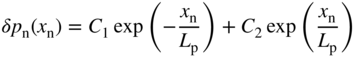
where C 1 and C 2 are constants. Since the base is finite in extent, we cannot argue the elimination of one term and both terms must be used. Applying our two boundary conditions to Eq. 8.2 we obtain
and
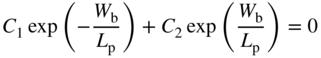
Solving for C 1 and C 2 we obtain
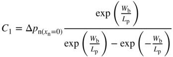
and

Substituting C 1 and C 2 into Eq. 8.2 we have

This can be plotted as shown in Figure 8.5.
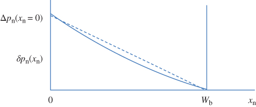
Figure 8.5 Plot of excess carrier concentration in the base under normal operating conditions for a PNP BJT
In order to calculate the current flow through the base, we consider minority hole diffusion current density (Eq. (2.65)) and we assume a BJT junction area A to obtain

Substituting δp(x n) from Eq. 8.2 and evaluating I p(x n) at x n = 0 we obtain

and evaluating I p(x n) at x n = W b we obtain

Using Eqs. 8.3 and 8.4 we can write I p(0) and I p(W b) as
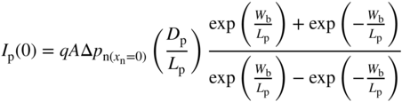
and

Note that
I
p(0) and
I
p(x
n) are determined by the slopes of the curve in Figure 8.5 at
x
n = 0 and at
x
n = W
b,
respectively. We require that ![]() and only a small fraction of the holes entering the base from the emitter junction recombine before they reach the base–collector junction. This therefore implies that the two slopes are similar. As a BJT becomes more close to ideal in performance, the shape of the curve approaches a straight line shown as a dotted line in Figure 8.5.
and only a small fraction of the holes entering the base from the emitter junction recombine before they reach the base–collector junction. This therefore implies that the two slopes are similar. As a BJT becomes more close to ideal in performance, the shape of the curve approaches a straight line shown as a dotted line in Figure 8.5.
The holes that do recombine in the base cause a base current to flow. This is because for every hole that recombines in the base, an electron must be supplied to the base to maintain base change neutrality. These electrons are supplied to the base from the external circuit resulting in base current flowing out of the base. Another contribution to base current exists due to electrons being injected from the base into the emitter. Since we have intentionally specified base doping much lower than emitter doping in the p+–n emitter–base junction, this electron injection current will be small. See Example 3.4 in which holes injected from a heavily doped p‐side into a lightly doped n‐side dominate current flow. The goal in BJT transistor design is to minimise total base current.
We will define the total base current as i B = I B + I n where I B represents electrons required for hole recombination in the base and I n represents electrons injected from the base to the emitter. We can quantify I B as the difference between the hole current entering the base and the hole current leaving the base and therefore
Using Eqs. 8.5 and 8.6, we obtain
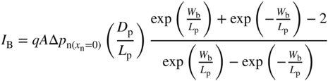
Since ![]() , a Taylor series expansion may be used for the exponential functions. To the second order,
, a Taylor series expansion may be used for the exponential functions. To the second order,
Upon substitution we obtain the approximation

This can be rewritten in terms of minority hole lifetime using L p 2 = D p τ p to yield

As expected, if the minority hole lifetime increases, less recombination will occur and base current decreases.
There is another way to approximate the base current. Using Figure 8.5 we can obtain the total charge in the base due to minority holes using the area under the curve. To simplify this, we will assume that the dotted line forming a triangular region allows us to use the area of a triangle ![]() to obtain
to obtain
Since this charge recombines on average in time τ p, the recombination current or base current becomes
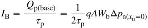
which is identical to Eq. 8.8.
We can now obtain a more complete view of the BJT and its performance and express this using a few key parameters.
The base transport factor B is the fraction of holes injected by the base–emitter junction that make it across the base to the base–collector junction and we therefore define B as

Typical values of base transport factor in a good BJT transistor approach unity. The value is maximised by minimising the base width and by doping the base lightly since increased doping causes undesirable carrier scattering and lowers minority carrier lifetimes and diffusion lengths in semiconductors. Note also that we can express I B in terms of B from Eq. 8.7 as
Since not all the current flowing through the base–emitter junction is hole current, we define the emitter injection efficiency γ as

where I n is due to electron injection into the emitter from the emitter–base junction. The value of emitter injection efficiency also approaches unity and is maximised by having a high emitter doping level and a low base doping level.
The ratio between collector current and emitter current is called the current transfer ratio α and is given by

which also approaches unity for a good BJT transistor. The terminal currents flowing in or out of the BJT terminals are labelled using lower case symbols as shown in Figure 8.3.
The total base current i B is now attributable to both minority hole recombination in the base and electron injection from base to emitter. Hence,
An important parameter that determines the current amplification available in a transistor is the collector current amplification factor β defined as

Dividing both numerator and denominator on the right‐hand side by I p(0) + I n we obtain

Since α is almost unity, typical values of β are large and can be on the order of 100. In this case a base current of 1 mA for a BJT would result in a collector current of 100 mA.
The resulting electrical behaviour of a PNP transistor may now be presented by a family of characteristic curves shown in Figure 8.6. Each curve shows the collector current for a given value of base current.

Figure 8.6
Plot of collector current  versus collector–emitter voltage
  for a typical PNP BJT.
  is negative since the base–collector junction is reverse‐biased. See Figure 8.3. The collector current amplification factor
  for this transistor can be read from the graph to be approximately 45. Note that collector current slightly increases with increasing collector voltage: As the reverse bias on the collector–emitter junction increases, the effective base width
  narrows which slightly increases base transport factor
Although we have presented a PNP transistor, the converse transistor type, the NPN transistor, operates in a completely analogous manner. In the NPN transistor, the minority carriers crossing the p‐type base are electrons rather than holes. Since electrons have higher diffusion lengths than holes in silicon, NPN transistors generally outperform PNP transistors, although both transistor types are used.
8.3 Junction Field‐Effect Transistor
The JFET is also built on the basis of the p–n junction, but its operating principle is quite different from that of a BJT. Instead of using minority carriers, it relies on current flow due to majority carriers. Control of current flow is provided by changing the cross‐sectional area of a channel through which majority carriers flow. By reducing the channel width to virtually zero, the flow of current can be minimised and by maximising the channel width, a maximum current can flow.
In Chapter 3, we saw that the depletion width of a p–n junction depends on a reverse bias. If reverse‐biased junctions are arranged on either side of a channel, the effective width of the channel can be controlled by means of the reverse bias voltage applied to the p–n junctions.
Figure 8.7 shows an n‐type channel of width h located between two p+ regions. The equilibrium depletion regions of width W for the two resulting p+n junctions are shown using dashed lines. They extend further into the n‐type region than into the p+ regions as expected. See Example 3.2.

Figure 8.7
Diagram of n‐channel JFET. Channel width  is defined as the portion of the n‐region of thickness
  that remains un‐depleted between two depletion regions each having width
  . The depletion region boundaries are shown as dotted lines. For convenience, we define source voltage
The n‐type material has ohmic contacts at the beginning and end of the channel. These are labelled source (S) and drain (D), and the channel carries the load current. The two p‐type regions are connected together, and they are connected to a gate (G) electrode using two ohmic contacts.
The resulting JFET characteristic curves are shown in Figure 8.8.
Figure 8.8 Family of characteristic curves for the n‐channel JFET of Figure 8.7
To understand and model this graph, we will start by confining our analysis to the behaviour closer to the origin. Consider the case in which V S = 0 and V D is small. As the gate voltage is made negative relative to the source region and the drain region, the two p–n junctions become reverse‐biased and the depletion regions of the two p–n junctions increase in width. See Figure 3.19. This decreases the effective channel width h. As gate voltage continues to become more negative, h will reach zero and the channel width reaches zero.
An expanded version of Figure 8.8 is shown in Figure 8.9 in which V DS = V D − V S is small. In this regime, we can consider the width h of the channel to be constant along the channel. For convenience, we shall again set V S = 0 and therefore we can state that V D ≅ V S = 0. The width W of a depletion region with bias was derived in Chapter 3 and using Eq. (3.26) we obtain


Figure 8.9
Detail of Figure 8.8 for small values of  . The approximately straight lines have slopes that depend on
  according to Eq. 8.9. This is often referred to as the linear region of JFET operation
If the doping in the p+ regions is much higher than the doping in the n‐type channel, we can assume that the depletion regions exist almost entirely within the n‐type region. Hence, from Figure 8.7, we can express channel width h as
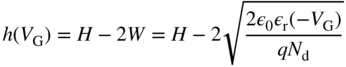
Note that the channel width h reaches zero when H = 2W . We define this condition as pinch‐off which is achieved if H − 2W = 0. Solving for the corresponding gate voltage we obtain

where pinch‐off voltage V p is defined as the magnitude of gate voltage at pinch‐off.
The electrical resistance R between source and drain of a channel of length L is therefore
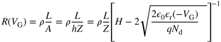
where A is the cross‐sectional area of the channel and Z is the channel depth. For the JFET of Figure 8.9 the curve having the smallest slope is for the case of a channel very close to the pinch‐off condition and hence V p ≅ 4 V for this JFET. Since the slope of each line in Figure 8.9 is equal to 1/R , we can express it as
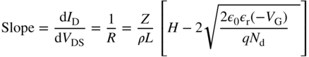
Equation 8.9 and corresponding Figure 8.9 represent widely applicable voltage‐controlled resistor behaviour. Depending on gate voltage, the resistance between drain and source varies. If the FET is connected such that drain current I D flows through a load, then the FET can control load current. A particular advantage of a JFET is that gate current is negligible since the p+n junctions are never forward‐biased during normal operation.
We can also consider larger values of V DS which are included in Figure 8.8. Modelling a JFET over a wide range of voltages is more complicated since the channel width is no longer uniform from source to drain. As the drain voltage shown in Figure 8.7 becomes more positive, it adds a further reverse bias to the p+n junctions near the drain contact thereby narrowing the channel width at the drain end of the JFET. Figure 8.10 shows the tapered shape of a channel with V G = 0 under these circumstances that reaches pinch‐off at the drain. Further increasing V DS will no longer substantially increase drain current and the JFET is said to be in saturation. Figure 8.11 shows the point on each characteristic curve of the JFET at the onset of saturation.

Figure 8.10
The tapered shape of a channel with  sufficient to cause the onset of pinch‐off at the drain.
  and
and  V for the JFET of Figure 8.8. Further increasing
  will no longer substantially increase drain current and the JFET is said to be in saturation

Figure 8.11
Black circles show the onset of saturation for each characteristic curve of Figure 8.8. Note that when  pinch‐off occurs at
  V. For
  V there is saturation and little increase in drain current. Corresponding points in the case of
  ,
,  , and
, and  V occur at
  ,
,  , and 1 V respectively. When
  V the channel is almost completely pinched off for all values of
More complete JFET modelling requires two‐dimensional treatment of the tapered channel to obtain the conductivity of the channel of varying cross‐sectional area. It is made still more complex due to carrier velocity effects since at pinch‐off, drain current I D is crowded into a very narrow channel. Electric fields in this portion of the channel can be sufficiently high that carrier velocity saturation occurs, especially in short channel JFETs. See Figure 2.24.
The converse JFET device has a p‐type channel between two n+p junctions, and its modes of operation are completely analogous to the n‐channel JFET. Both n‐channel and p‐channel JFETs are in use. Variations on the JFET design we have described also exist. For example, JFETs may be fabricated in which the channel is formed between only one p–n junction and an insulating layer on the opposing side of the channel. The same operating principle still applies.
8.4 BJT and JFET Symbols and Applications
Figure 8.12 shows both PNP and NPN BJT transistor symbols as well as n‐channel and p‐channel JFET symbols.

Figure 8.12 Symbols for BJT and JFET transistors
Today's electronics industry is dominated by digital electronics and the MOSFET (metal oxide field‐effect transistor) serves almost all of this market. The MOSFET is a variation of the JFET and is covered in detail in semiconductor device books. See Further Reading.
There are, however, many other more specialised applications of transistors in linear amplifiers, temperature sensors, low‐noise amplifiers, analogue switches, and power electronics for which BJTs and JFETs can outperform MOSFETs. The p–n junctions common to both the BJT and the JFET are very robust, and these devices are more rugged and less prone to damage than are MOSFETs. JFETs have inherently lower noise operation than MOSFETs. The BJT is widely used in discrete applications due to the very broad selection of individually packaged BJT types available covering a wide spectrum of applications from small signal amplifiers to power electronics. The BJT is also used in very high frequency applications, such as radio frequency circuits for wireless communications systems. As a temperature sensor, the BJT, due to its well understood temperature dependence, is widely used.
8.5 Summary
- Two well‐known transistor types include the BJT and the JFET. These devices both take advantage of the detailed properties of p–n junctions.
- The BJT uses a reverse‐biased p–n junction and controls the reverse current through this diode by means of another forward‐biased p–n junction in close proximity to the reverse‐biased p–n junction
- Modelling the BJT requires examining the base region of the device. The base region is common to both p–n junctions in the device. The minority carrier concentration must be calculated within this base region in order to calculate the current flow through the device.
- Current flow between the emitter and the collector of the BJT is shown to be controlled using the base electrode. Base current can be calculated and by suitably designing the BJT, base current can be minimised. Collector current is related to base current by the collector current amplification factor β .
- The JFET operates on a very different principle from the BJT. A channel formed laterally between two p–n junctions carries current between a source electrode and a drain electrode. A gate electrode allows reverse bias to be simultaneously applied to both p–n junctions.
- Increasing the reverse bias on the two p–n junctions causes their depletion widths to increase. This causes the channel to be narrowed, thereby restricting the current flow between source and drain. In this manner, the JFET operates as a voltage‐controlled resistor provided drain voltages are small.
- For higher drain voltages, the JFET channel becomes tapered and current flow between source and drain is more complicated to calculate. Above a pinch‐off voltage, the device goes into saturation. Beyond saturation, the channel remains pinched off and drain current does not significantly increase further with increasing drain voltage.
- Both PNP and NPN versions of the BJT exist, and both n‐channel and p‐channel JFETs exist. Although not as widely used as MOSFETS, BJTs and JFETs remain popular in a variety of specialised electronics applications such as low‐noise amplifiers and very high frequency circuits. The BJT, in particular, is widely used as a discrete transistor component.
Further Reading
- Neamen, D.A. (2003). Semiconductor Physics and Devices, 3e. McGraw Hill.
- Roulston, D.J. (1999). An Introduction to the Physics of Semiconductor Devices. Oxford University Press.
- Streetman, B.G. and Banerjee, S.K. (2015). Solid State Electronic Devices, 7e. Pearson.
Problems
-
8.1 A PNP BJT has emitter doping 100 times larger than base doping. The base width is much smaller than the carrier diffusion length.
- Assuming that we increase base doping by a factor of 10. Qualitatively, what effect will this have on the collector current if any? Why?
- Assume that we decrease base width by a factor of 2. Qualitatively, what effect will this have on collector current?
- 8.2 Calculate and plot the excess hole concentration in the base of a PNP BJT as a function of position assuming W b/L p = 0.2. Use spreadsheet software. You can assume a value of Δp E = 1 × 1015 cm−3 and assume Δpc = 0. Your horizontal axis can be expressed in dimensionless units of W b/L p and range between 0 and 0.2.
-
8.3 A PNP BJT has the following properties at room temperature:
Carrier lifetimes of 0.1 μs
Emitter doping 1019 cm−3
Collector doping 1017 cm−3
Base doping 1017 cm−3
Metallurgical base width (junction to junction based on a step doping profile): 4 μm
Cross‐sectional area 10−3 cm2
- Calculate the depletion width at the collector–base junction with V CB = −50 V
- Calculate B for the transistor with V CB = −50 V
- Calculate γ for the transistor with V CB = −50 V
- Calculate β for the transistor with V CB = −50 V
-
Plot the excess hole concentration in the base region for the following conditions:
- I C = 1 μA
- (ii) I C = 1 mA
- (iii) Calculate the hole charge in the base for each of (i) and (ii). Use these values to estimate β and compare this to the answer you obtained in part (d). Explain any discrepancy carefully.
- Sketch the ideal collector characteristics for the transistor ( i C versus V CE). Let i B vary from zero to 0.2 mA in increments of 0.02 mA. Let V CE vary from 0 to −50 V.
- Explain how it is possible for the average time an injected hole spends in transit across the base to be shorter than the hole lifetime in the base.
- Repeat parts (a)–(d) for an NPN transistor with the same doping levels.
- Why are NPN transistors preferred if there is a choice?
-
8.4 Look up further information as needed in Further Reading or using the internet to answer the following questions:
- Find the meanings of ‘saturation’ and ‘oversaturation’ as applied to the BJT.
- Explain why the turn‐on time of a BJT is faster when the transistor is driven into oversaturation.
- Explain why the turn‐off time of a BJT is slower after it had been driven into oversaturation.
- Explain why PNP transistors are frequently needed in circuits that also contain NPN transistors.
-
8.5 A symmetrical P+ NP+ transistor is connected in four ways to a DC voltage source producing voltage V between +V and ground as shown in the table. Assume that V > kT/q.
Configuration Collector Base Emitter 1 ground No connection +V 2 ground ground +V 3 +V ground No connection 4 +V ground +V - Sketch a diagram for each connection scheme using the appropriate BJT symbol in Figure 8.12.
- Sketch δp n(x n) in the base region for each case.
- Explain how you can justify each sketch in part (b).
- Which situation is most likely to exist in a real transistor application? Why?
-
8.6 An n‐channel JFET is described as follows:
Semiconductor is silicon at room temperature
p+ doping: 5 × 1018 cm−3
n doping: 2 × 1016 cm−3
L = 100 μm
The JFET is biased such that V S = V D = 0
- Find the value of H in Figure 8.7 that would cause the channel to reach pinch‐off when V G = − 4 V.
-
Using the value of
H
obtained in (a), calculate the resistance of the channel from source to drain for each of the following voltages:
- V G = − 3 V
- V G = − 2 V
- V G = − 1 V
- V G = 0
- Calculate the maximum drain voltage V D that could be applied to the FET with V G = − 2 V such that the channel width h remains at 90% of its width at the source‐end of the JFET. Use the value of H obtained in (a) and continue to assume that V S = 0.
- 8.7 Look into Further Reading or similar resources to find a full derivation of JFET channel resistance for a tapered channel. Obtain a good understanding of the model and its limitations and understand the mathematical justification for the range of validity of the model. Present and explain the model in your own written document.
-
8.8 Look up further information as needed in Further Reading or using the Internet and answer the following questions:
- The JFET is often referred to a depletion mode transistor. Explain the origin of this terminology.
- Explain why the JFET has a much higher input impedance than the BJT. What values of input impedance are typical for JFETs? Why is this important?