
CHAPTER 4
Interfacing Electronics
This chapter introduces you to the type of practical electronics that you need to work correctly and effectively in interfacing electronic circuits with the Beagle boards. The chapter begins by describing some equipment that can be helpful in developing and debugging electronic circuits. It continues with a practical introductory guide to circuit design and analysis, in which you are encouraged to build the circuits and utilize the equipment that is described at the beginning of the chapter. The chapter continues with a discussion on the typical discrete components that can be interfaced to the general-purpose input/outputs (GPIOs) on the Beagle boards, including diodes, capacitors, transistors, optocouplers, switches, and logic gates. Finally, the important principles of analog-to-digital conversion (ADC) are described, as such knowledge is required to interface to the Beagle board ADCs.
EQUIPMENT REQUIRED FOR THIS CHAPTER:
- Components for this chapter (if following along): The full list is provided at the end of this chapter.
- Digilent Analog Discovery (version 1 or 2) or access to a digital multimeter, signal generator, and oscilloscope.
Further details on this chapter are available at www.exploringbeaglebone.com/chapter4/.
Analyzing Your Circuits
When developing electronics circuits for the Beagle boards, it is useful to have the following tools so that you can analyze a circuit before you connect it to the board's inputs/outputs to reduce the chance of damaging your board. In particular, it is useful to have access to a digital multimeter and a mixed-signal oscilloscope.
Digital Multimeter
A digital multimeter (DMM) is an invaluable tool for measuring the voltage, current, and resistance/continuity of circuits. If you don't already have one, try to purchase one with the following features:
- Auto power off: It is easy to waste batteries.
- Auto range: It is vital that you can select different measurement ranges. Midprice meters often have automatic range selection functionality that can reduce the time required to take measurements.
- Continuity testing: This feature should provide an audible beep unless there is a break in the conductor (or excessive resistance).
- True RMS readings: Most low-cost meters use averaging to calculate AC(~) current/voltage. True RMS meters process the readings using a true root mean square (RMS) calculation, which makes it possible to account for distortions in waveforms when taking readings. This feature is useful for analyzing phase controlled equipment, solid-state devices, motorized devices, etc.
- Other useful options: These options are not strictly necessary but are helpful: backlit display, a measurement hold, large digit displays, a greater number of significant digits, PC connectivity (ideally optoisolated), temperature probe, and diode testing.
- Case: Look for a good-quality rubberized plastic case.
Generally, most of the preceding features are available on midprice DMMs with a good level of accuracy (1 percent or better), high input impedances (>10 MΩ), and good measurement ranges. High-end multimeters mainly offer faster measurement speed and greater levels of measurement accuracy; some may also offer features such as measuring capacitance, frequency, temperature using an infrared sensor, humidity, and transistor gain. Some of the best known brands are Fluke, Tenma, Agilent, Extech, and Klein Tools.
Oscilloscopes
Standard DMMs provide you with a versatile tool that enables you to measure average voltage, current, and resistance. Oscilloscopes typically only measure voltage, but they enable you to see how the voltage changes with respect to time. Typically, you can simultaneously view two or more voltage waveforms that are captured within a certain bandwidth and number of analog samples (memory). The bandwidth defines the range of signal frequencies that an oscilloscope can measure accurately (typically to the 3 dB point, i.e., the frequency at which a sine wave amplitude is ~30 percent lower than its true amplitude). To achieve accurate results, the number of analog samples needs to be a multiple of the bandwidth (you will see why later in this chapter when the Nyquist rate is discussed); and for modern oscilloscopes, this value is typically four to five times the bandwidth, so a 25 MHz oscilloscope should have 100 million samples per second or greater. The bandwidth and number of analog samples have the greatest influence on the cost of an oscilloscope.
Several low-cost two-channel oscilloscopes are available, such as those by Owon PDS5022S 25 MHz (~$200), feature-rich Siglent SDS1022DL 25 MHz (~$325), Rigol DS1052 50 MHz (~$325), and Owon SDS6062 60 MHz (~$349). Prices rise considerably as the bandwidth increases, to around $1,500 for a 300 MHz scope. Agilent digital storage (DSOX) and mixed-signal (MSOX) series scopes would be considered to be mid/high range and cost $3,000 (100 MHz) to $16,000 (1 GHz). Mixed-signal scopes also provide you with digital bus analysis tools.
The Digilent Analog Discovery 2 with Waveforms (see Figure 4-1) is used to test all the circuits in this book. The Analog Discovery (and similar Analog Discovery 2) is a USB oscilloscope, waveform generator, digital pattern generator, and logic analyzer for the Windows environment. The recently released Waveforms software now has support for Linux (including ARM) and macOS. The Analog Discovery 2 is generally available for $279. If you are starting out or refreshing your electronics skills, it is a really great piece of equipment for the price.
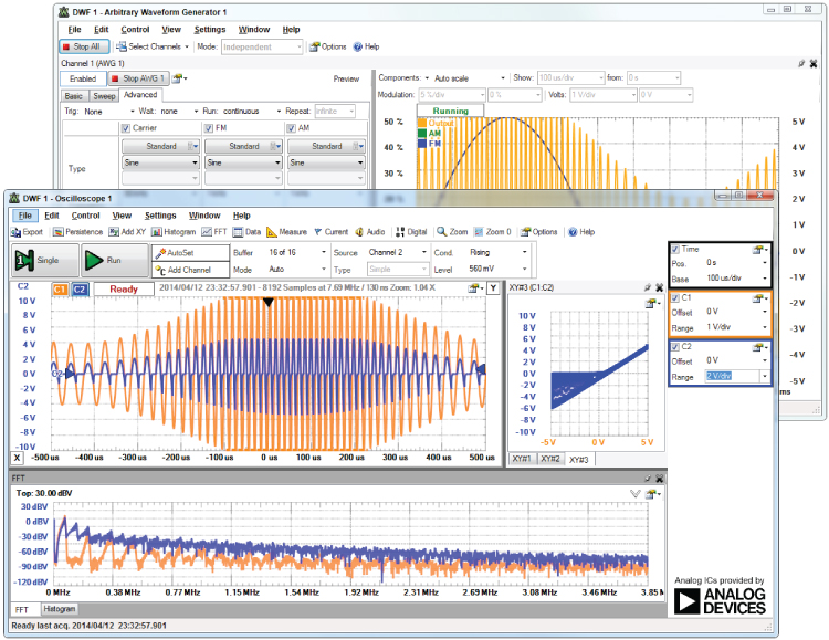
Figure 4-1: The Waveforms application generating a signal and displaying the response from the physical circuit
The Analog Discovery is used to generate all the oscilloscope plots that are presented in this book, as all examples have been implemented using real circuits. The scope is limited to two channels at 5 MHz per channel and 50 million samples per second, for both the waveform generator and the differential oscilloscope. As such, the Analog Discovery is mainly focused on students and learners; however, it can also be useful in deciding upon “must-have” features for your next, more expensive, equipment.
There are alternative mixed-signal USB scopes, such as PicoScopes, which range from $160 to $10,000 (www.picotech.com), and the BitScope DSO, from $150 to $1,000 (www.bitscope.com), which has Linux support. However, based on the feature set that is currently available on USB oscilloscopes, it may be the case that a bench scope with a USB logic analyzer provides the best “bang for your buck.”
Basic Circuit Principles
Electronic circuits contain arrangements of components that can be described as being either passive or active. Active components, such as transistors, are those that can adaptively control the flow of current, whereas passive components cannot (e.g., resistors, capacitors, diodes). The challenge in building circuits is designing a suitable arrangement of appropriate components. Fortunately, there are circuit analysis equations to help you.
Voltage, Current, Resistance, and Ohm's Law
The most important equation that you need to understand is Ohm's law. It is simply stated as follows:
where:
- Voltage (V), measured in volts (V), is the difference in potential energy that forces electrical current to flow in the circuit. A water analogy is useful when thinking of voltage; many houses have a buffer tank of water in the attic that is connected to the taps in the house. Water flows when a tap is turned on due to the height of the tank and the force of gravity. If the tap were at the same height as the top of the tank of water, no water would flow because there would be no potential energy. Voltage behaves in much the same way; when a voltage on one side of a component, such as a resistor, is greater than on the other side, electrical current can flow across the component.
- Current (I), measured in amps (A), is the flow of electrical charge. To continue the water analogy, current would be the flow of water from the tank (with a high potential) to the tap (with a lower potential). Remember that the tap still has potential and water will flow out of the drain of the sink, unless it is at ground level (GND). To put the level of current in context, when we build circuits to interface with the Beagle board's GPIOs, they usually source or sink only about 5 mA, where a milliamp is one thousandth of an amp.
- Resistance (R), measured in ohms (Ω), discourages the flow of charge. A resistor is a component that reduces the flow of current through the dissipation of power. It does this in a linear fashion, where the power dissipated in watts (W), is given by
 or, alternatively, by integrating Ohm's law:
 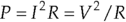 . The power is dissipated in the form of heat, and all resistors have a maximum dissipated power rating. Common metal film or carbon resistors typically dissipate 0.125 W to 1 W, and the price increases dramatically if this value has to exceed 3 W. To finish with the water analogy, resistance is the friction between the water and the pipe, which results in a heating effect and a reduction in the flow of water. This resistance can be increased by increasing the surface area over which the water has to pass, while maintaining the pipe's cross-sectional area (e.g., placing small pipes within the main pipe).
As an example, if you had to buy a resistor that limits the flow of current to 100 mA when using a 5 V supply, as illustrated in Figure 4-2(a), which resistor should you buy? The voltage dropped across the resistor, VR
, must be 5 V, as it is the only component in the circuit. Because ![]() , it follows that the resistor should have the value
, it follows that the resistor should have the value ![]() , and the power dissipated by this resistor can be calculated using any of the general equations
, and the power dissipated by this resistor can be calculated using any of the general equations ![]() as 0.5 W.
as 0.5 W.
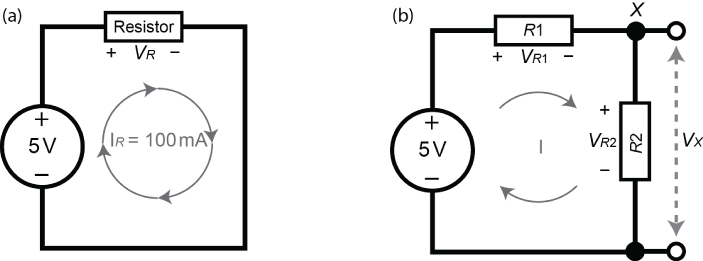
Figure 4-2: (a) Ohm's law circuit example, and (b) a voltage divider example
Buying one through-hole, fixed-value ![]() metal-film resistor with a 1 percent tolerance (accuracy) costs about $0.10 for a 0.33 W resistor and $0.45 for a 1 W power rating. You should be careful with the power rating of the resistors you use in your circuits, as underspecified resistors can blow. A 30 W resistor will cost $2.50 and can get extremely hot—not all resistors are created equally!
metal-film resistor with a 1 percent tolerance (accuracy) costs about $0.10 for a 0.33 W resistor and $0.45 for a 1 W power rating. You should be careful with the power rating of the resistors you use in your circuits, as underspecified resistors can blow. A 30 W resistor will cost $2.50 and can get extremely hot—not all resistors are created equally!
Voltage Division
If the circuit in Figure 4-2(a) is modified to add another resistor in series, as illustrated in Figure 4-2(b), what will be the impact on the circuit?
- Because one resistor is after the other (they're in series), the total resistance that the current must pass through to circulate in the circuit is the sum of the two values:
 .
. - The supply voltage must drop across the two resistors, so you can say that
 . The voltage that drops across each resistor is inversely proportional to the resistor's value. This circuit is called a voltage divider.
Suppose you want to calculate on paper the voltage value at point X in Figure 4-2(b) if R1 = 25 Ω and R2 = 75 Ω. The total resistance in the circuit is ![]() , and the total voltage drop across the resistors must be 5 V; therefore, by using Ohm's law, the current flowing in the circuit is I = V/R = 5 V/100 Ω = 50 mA. If the resistance of R1 is 25 Ω, then the voltage drop across
, and the total voltage drop across the resistors must be 5 V; therefore, by using Ohm's law, the current flowing in the circuit is I = V/R = 5 V/100 Ω = 50 mA. If the resistance of R1 is 25 Ω, then the voltage drop across ![]() and the voltage drop across
and the voltage drop across ![]() . You can see that the sum of these voltages is 5 V, thus obeying Kirchoff's voltage law, which states that the sum of the voltage drops in a series circuit equals the total voltage applied.
. You can see that the sum of these voltages is 5 V, thus obeying Kirchoff's voltage law, which states that the sum of the voltage drops in a series circuit equals the total voltage applied.
To answer the question fully, in this circuit, 1.25 V is dropped across R1 and 3.75 V is dropped across R2, so what is the voltage at X? To know that, you have to measure X with respect to some other point! If you measured X with respect to the negative terminal of the supply, the voltage drop is VX in Figure 4-2(b), and it is the same as the voltage drop across R2, so it is 3.75 V. However, it would be equally as valid to ask the question, “What is the voltage at X with respect to the positive terminal of the supply?” In that case, it would be the negative of the voltage drop across R1 (as X is at 3.75 V with respect to the negative terminal and the positive terminal is at +5 V with respect to the negative terminal); therefore, the voltage at X with respect to the positive terminal of the supply is −1.25 V.
To calculate the value of VX in Figure 4-2(b), the voltage divider rule can be generalized to the following:
You can use this rule to determine a voltage VX, but unfortunately this configuration is quite limited in practice, because it is likely that the circuit to which you connect this voltage supply, VX, will itself have a resistance (or load). This will alter the characteristic of your voltage divider circuit, changing the voltage VX. However, most circuits that follow voltage dividers are usually input circuits that have very high input impedances, and therefore the impact on VX will be minimal.
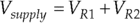
Figure 4-3(a) captures a variable resistor, or potentiometer (pot), and an associated circuit where it is used as a stand-alone voltage divider. The resistance between pins 1 and 3 is a fixed value, 10 kΩ in the case of the multiturn pot; however, the resistance between pins 3 and the wiper pin (pin 2) varies between 0 Ω and 10 kΩ. Therefore, if the resistance between pins 2 and 3 is 2 kΩ, then the resistance between pins 1 and 2 will be 10 kΩ − 2 kΩ = 8 kΩ. In such a case, the output voltage, Vout , will be 1 V, and it can be varied between 0 V and 5 V by turning the small screw on the pot, using a trim tool or screwdriver.
Figure 4-3: (a) Potentiometers and using a variable voltage supply, and (b) a current divider example
Current Division
If the circuit is modified as in Figure 4-3(b) to place the two resistors in parallel, you now have a current divider circuit. Current will follow the path of least resistance, so if R1 = 100 Ω and R2 = 200 Ω, then a greater proportion of the current will travel through R1. So, what is this proportion? In this case the voltage drop across R1 and R2 is 5 V in both cases. Therefore, the current I1 will be I = V/R = 5 V/100 Ω = 50 mA, and the current I2 will be I = 5 V/200 Ω = 25 mA. Therefore, twice as much current travels through the 100 Ω resistor as the 200 Ω resistor. Clearly, current favors the path of least resistance.
Kirchoff's current law states that the sum of currents entering a junction equals the sum of currents exiting that junction. This means that IS = I1 + I2 = 25 mA + 50 mA = 75 mA. The current divider rule can be stated generally as follows:
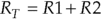
However, this requires that you know the value of the current I (IS in this case) that is entering the junction. To calculate IS directly, you need to calculate the equivalent resistance (RT) of the two parallel resistors, which is given as follows:
This is 66.66 Ω in Figure 4-3(b); therefore IS = V/R = 5 V/66.66 Ω = 75 mA, which is consistent with the initial calculations.
The power delivered by the supply: ![]() This should be equal to the sum of the power dissipated by
This should be equal to the sum of the power dissipated by ![]() and
and ![]() , giving 0.375 W total, confirming that the law of conservation of energy applies!
, giving 0.375 W total, confirming that the law of conservation of energy applies!
Implementing Circuits on a Breadboard
The breadboard is a great platform for prototyping circuits, and it works perfectly with the Beagle boards. Figure 4-4 illustrates a breadboard, describing how you can use the two horizontal power rails for 3.3 V and 5 V power. The GPIO header on the Beagle boards typically consists of female header pins, which means you can use wire strands to make connections.
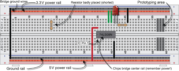
Figure 4-4: The breadboard with a 7408 IC (quad two-input AND gates)
A good-quality breadboard like that in Figure 4-4 (830 tie points) costs about $6 to $10. Giant breadboards (3,220 tie points) are available for about $20. Here are some tips for using breadboards:
- Whenever possible, place pin 1 of your ICs on the bottom left so that you can easily debug your circuits. Always line up the pins carefully with the breadboard holes before applying pressure and “clicking” it home. Also, ICs need power!
- Leaving a wire disconnected is not the same as connecting it to GND (discussed later in this chapter).
- Use a flat-head screwdriver to slowly lever ICs out of the breadboard from both ends to avoid bending the IC's legs.
- Be careful not to bridge resistors and other components by placing two of their pins in the same vertical rail. Also, trim resistor leads before placing them in the board, as long resistor leads can accidentally touch and cause circuit debugging headaches.
- Momentary push buttons typically have four legs that are connected in two pairs; make sure that you orient them correctly (use a DMM continuity test).
- Staples make great bridge connections!
- Some boards have a break in the power rails; bridge this where necessary.
- Breadboards typically have 0.1" spacing (lead pitch) between the tie points, which is 2.54 mm metric. Try to buy all components and connectors with that spacing. For ICs, choose the DIP/PDIP (the IC code ends with an N); and for other components, choose the “through-hole” form.
- Use the color of the hook-up wire to mean something—e.g., use red for 5 V and black for GND; it can really help when debugging circuits. Solid-core 22AWG wire serves as perfect hook-up wire and is available with many different insulator colors. Pre-formed jumper wire is available, but long wires lead to messy circuits. A selection of hook-up wire in different colors and a good-quality wire-stripping tool enables the neatest and most stable breadboard layouts.
Digital Multimeters and Breadboards
Measuring voltage, current, and resistance is fairly straightforward once you take a few rules into account (with reference to Figure 4-6):
- DC voltage (DCV) is measured in parallel with (i.e., across) the component that experiences the voltage drop. The meter should have the black probe in the COM (common) DMM input.
- DC current (DCA) is measured in series, so you will have to “break” the connection in your circuit and wire the DMM as if it were a component in series with the conductor in the circuit in which you are measuring current. Use the black probe lead in COM and the red lead in the μAmA input (or equivalent). Do not use the 10 A unfused input.
- Resistance cannot usually be measured in-circuit, because other resistors or components will act as parallel/series loads in your measurement. Isolate the component and place your DMM red probe in the VΩ input and set the meter to measure Ω. The continuity test can be reasonably effectively used in-circuit, provided that it is de-energized.
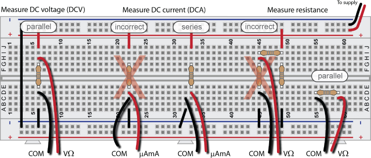
Figure 4-6: Measuring voltage, current, and resistance
If your DMM is refusing to function, you may have blown the internal fuse. Disconnect the DMM probes and open the meter to find the small glass fuse. If you have a second meter, you can perform a continuity test to determine whether it has blown. Replace it with a like value (or PTC)—not a mains fuse!
Example Circuit: Voltage Regulation
Now that you have read the principles, a more complex circuit is discussed in this section, and then the components are examined in detail in the following sections. Do not build the circuit in this section; it is intended as an example to introduce the concept of interconnected components.
A voltage regulator is a complex but easy-to-use device that accepts a varied input voltage and outputs a constant voltage almost regardless of the attached load, at a lower level than the input voltage. The voltage regulator maintains the output voltage within a certain tolerance, preventing voltage variations from damaging downstream electronics devices.
The Beagle boards have an advanced Power Management IC (PMIC) that can supply different voltage levels to different devices at different output pins. For example, there is a 5 V output, a 3.3 V output, and a 1.8 V reference for the analog-to-digital converters. You can use the 5 V and 3.3 V supplies on the board to drive your circuits, but only within certain current supply limits. The BBB can supply up to 1 A on the VDD_5V pins on the P9 header (pins 5 and 6) if the BBB is connected to a DC power supply via the 5 V jack, and 250 mA on the DC_3.3V pins (pins 3 and 4).
If you want to draw larger currents for applications like driving motors, you may need to use voltage regulators like that in Figure 4-7. You can build this directly on a breadboard or you can purchase a “breadboard power supply stick 5 V/3.3 V” from SparkFun (www.sparkfun.com) for about $15.
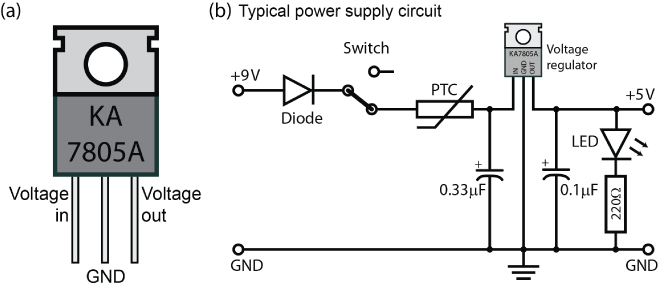
Figure 4-7: (a) The KA7805A/LM7805 voltage regulator, and (b) an example regulator circuit
As shown in Figure 4-7, the pin on the left of the regulator is the voltage supply input. When delivering a current of 500 mA, the KA7805/LM7805 voltage regulator will accept an input voltage range of 8 V–20 V, and will output a voltage (on the right) in the range of 4.8 V–5.2 V. The middle pin should be connected to the ground rail. The aluminum plate at the back of the voltage regulator is there to dissipate heat. The hole enables you to bolt on a heat sink, allowing for greater output currents, of up to 1 A.
The minimum input voltage required is about 8 V to drive the KA7805/LM7805 voltage regulator. If your supply voltage is lower than that, then you could use a low-dropout (LDO) voltage regulator, which can require a supply as low as 6 V to operate a 5 V regulator. The implementation circuit in Figure 4-7 has the following additional components that enable it to deliver a clean and steady 5 V, 1 A supply:
- The diode ensures that if the supply is erroneously connected with the wrong polarity (e.g., 9 V and GND are accidentally swapped), then the circuit is protected from damage. Diodes like the 1N4001 (1 A supply) are very low cost, but the downside is that there will be a small forward voltage drop (approximately 1 V at 1 A) across the diode in advance of the regulator.
- The switch can be used to power the circuit on or off. A slider switch enables the circuit to remain continuously powered.
- The Positive Temperature Coefficient (PTC) resettable fuse is useful for preventing damage from overcurrent faults, such as accidental short circuits or component failure. The PTC enables a holding current to pass with only a small resistance (about 0.25 Ω); but once a greater tripping current is exceeded, the resistance increases rapidly, behaving like a circuit breaker. When the power is removed, the PTC will cool (for a few seconds), and it regains its pre-tripped characteristics. In this circuit a 60R110 or equivalent Polyfuse would be appropriate, as it has a holding current of 1.1 A and a trip current of 2.2 A, at a maximum voltage of 60 V DC.
- The 0.33 μF capacitor is on the supply side of the regulator and the 0.1 μF capacitor is on the output side of the regulator. These are the values recommended in the datasheet to remove noise (ripple rejection) from the supply. Capacitors are discussed shortly.
- The LED and appropriate current-limiting resistor provide an indicator light that makes it clear when the supply is powered.
Discrete Components
The previous example circuit used a number of discrete components to build a stand-alone power supply circuit. In this section, the types of components that compose the power supply circuit are discussed in more detail. These components can be applied to many different circuit designs, and it is important to discuss them now, as many of them are used in designing circuits that interface to the Beagle board input/outputs in Chapter 6.
Diodes
Simply put, a diode is a discrete semiconductor component that allows current to pass in one direction but not the other. As the name suggests, a “semi” conductor is neither a conductor nor an insulator. Silicon is a semiconductive material, but it becomes much more interesting when it is doped with an impurity, such as phosphorus. Such a negative (n-type) doping results in a weakly bound electron in the valence band. It can also be positively doped (p-type) to have a hole in the valence band, using impurities such as boron. When you join a small block of p-type and n-type doped silicon together, you get a pn-junction—a diode! The free electrons in the valence band of the n-type silicon flow to the p-type silicon, creating a depletion layer and a voltage potential barrier that must be overcome before current can flow.
When a diode is forward biased, it allows current to flow through it; when it is reverse-biased, no current can flow. A diode is forward-biased when the voltage on the anode (+ve) terminal is greater than the voltage on the cathode (−ve) terminal; however, the biasing must also exceed the depletion layer potential barrier (knee voltage) before current can flow, which is typically between 0.5 V and 0.7 V for a silicon diode. If the diode is reverse-biased by applying a greater voltage on the cathode than the anode, then almost no current can flow (maybe 1 nA or so). However, if the reverse-biased voltage is increasingly raised, then eventually the diode will break down and allow current to flow in the reverse direction. If the current is low, then this will not damage the diode—in fact, a special diode called a Zener diode is designed to operate in this breakdown region, and it can be configured to behave just like a voltage regulator.
The 1N4001 is a low-cost silicon diode that can be used in a simple circuit (see Figure 4-8) to demonstrate the use and behavior of diodes. The 1N4001 has a peak reverse breakdown voltage of 50 V. In this circuit, a sine wave is applied that alternates from +5 V to −5 V, using the waveform generator of the Analog Discovery. When the Vin voltage is positive and exceeds the knee voltage, then current will flow, and there will be a voltage drop across the load resistor Vload , which is slightly less than Vin . There is a small voltage drop across the diode Vd and you can see from the oscilloscope measurements that this is 0.67 V, which is within the expected range for a silicon diode.
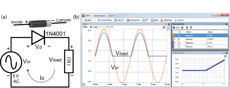
Figure 4-8: Circuit and behavior of a 1N4001 diode with a 5 V AC supply and a 1 kΩ load resistor
The diode is used in the circuit in Figure 4-7 as a reverse polarity protector. It should be clear from the plot in Figure 4-8 why it is effective, as when Vin is negative, the Vload is zero. This is because current cannot flow through the diode when it is reverse-biased. If the voltage exceeded the breakdown voltage for the diode, then current would flow; but since that is 50 V for the 1N4001, it will not occur in this case. Note that the bottom-right corner of Figure 4-8 shows an XY-plot of output voltage (y-axis) versus input voltage (x-axis). You can see that for negative input voltage the output voltage is 0, but once the knee voltage is reached (0.67 V), the output voltage increases linearly with the input voltage. This circuit is called a half-wave rectifier. It is possible to connect four diodes in a bridge formation to create a full-wave rectifier.
Light-Emitting Diodes
A light-emitting diode (LED) is a semiconductor-based light source that is often used as a state indication light in all types of devices. Today, high-powered LEDs are being used in car lights, in back lights for televisions, and even in place of filament lights for general-purpose lighting (e.g., home lighting, traffic lights, etc.) mainly because of their longevity and extremely high efficiency in converting electrical power to light output. LEDs provide useful status and debug information about your circuit, often used to indicate whether a state is true or false.
Like diodes, LEDs are polarized. The symbol for an LED is illustrated in Figure 4-9. To cause an LED to light, the diode needs to be forward biased by connecting the anode (+) to a more positive source than the cathode (−). For example, the anode could be connected to +3.3 V and the cathode to GND; however, also remember that the same effect would be achieved by connecting the anode to 0 V and the cathode to −3.3 V.
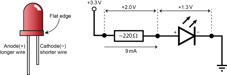
Figure 4-9: An LED example and a circuit to drive an LED with appropriate forward current and voltage levels
Figure 4-9 illustrates an LED that has one leg longer than the other. The longer leg is the anode (+), and the shorter leg is the cathode (−). The plastic LED surround also has a flat edge, which indicates the cathode (−) leg of the LED. This flat edge indication is particularly useful when the LED is in-circuit and the legs have been trimmed.
LEDs have certain operating requirements, defined by a forward voltage and a forward current. Every LED is different, and you need to reference the datasheet of the LED to determine these values. An LED does not have a significant resistance, so if you were to connect the LED directly across your Beagle board's 3.3 V supply, the LED would act like a short circuit, and you would drive a large current through the LED, damaging it—but more important, damaging your board! Therefore, to operate an LED within its limits you need a series resistor, called a current-limiting resistor. Choose this value carefully to maximize the light output of the LED and to protect the circuit.
Referring to Figure 4-9, if you are supplying the LED from the Beagle board's 3.3 V supply and you want to have a forward voltage drop of 1.3 V across the LED, you need the difference of 2 V to drop across the current-limiting resistor. The LED specifications require you to limit the current to 9 mA, so you need to calculate a current-limiting resistor value as follows:
As V = IR, then R = V/I = 2 V/0.009 A = 222 Ω
Therefore, a circuit to light an LED would look like that in Figure 4-9. Here a 220 Ω resistor is placed in series with the LED. The combination of the 3.3 V supply and the resistor drives a current of 9 mA through the forward-biased LED; as with this current the resistor has a 2 V drop across it, then accordingly the LED has a forward voltage drop of 1.3 V across it. Please note that this would be fine if you were connecting to the BBB's DC_3.3V output, but it is not fine for use with the BBB's GPIOs, as the maximum current that the BBB can source from a GPIO pin is about 4–6 mA. You will see a solution for this shortly, and again in Chapter 6.
It is also worth mentioning that you should not dim LEDs by reducing the voltage across the LED. An LED should be thought of as a current-controlled device, where driving a current through the LED causes the forward voltage drop. Therefore, trying to control an LED with a variable voltage will not work as you might expect. To dim an LED you can use a pulse-width modulated (PWM) signal, essentially rapidly switching the LED on and off. For example, if a rapid PWM signal is applied to the LED that is off for half of the time and on for half of the time, then the LED will appear to be only emitting about half of its regular operating condition light level. Our eyes don't see the individual changes if they are fast enough; they average over the light and dark interval to see a constant, but dimmer illumination.
Figure 4-10 illustrates a PWM square wave signal at different duty cycles. The duty cycle is the percentage of time that the signal is high versus the time that the signal is low. In this example, a high is represented by a voltage of 3.3 V and a low by a voltage of 0 V. A duty cycle of 0 percent means that the signal is constantly low, and a duty cycle of 100 percent means that the signal is constantly high.
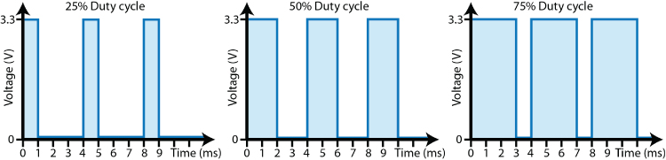
Figure 4-10: Duty cycles of pulse width modulation (PWM) signals
PWM can be used to control the light level of LEDs, but it can also be used to control the speed of DC motors, the position of servo motors, and many more applications. You will see such an example in Chapter 6 when the built-in PWM functionality of the Beagle boards is used.
The period (T) of a repeating signal (a periodic signal) is the time it takes to complete a full cycle. In the example in Figure 4-10, the period of the signal in all three cases is 4 ms. The frequency (f) of a periodic signal describes how often a signal goes through a full cycle in a given time period. Therefore, for a signal with a period of 4 ms, it will cycle 250 times per second (1/0.004), which is 250 hertz (Hz). We can state that f (Hz) = 1/T (s) or T (s) = 1/f (Hz). Some high-end DMMs measure frequency, but generally you use an oscilloscope to measure frequency. PWM signals need to switch at a frequency to suit the device to be controlled; typically, the frequency is in the kHz range for motor control.
Smoothing and Decoupling Capacitors
A capacitor is a passive electrical component that can be used to store electrical energy between two insulated plates when there is a voltage difference between them. The energy is stored in an electric field between the two plates, with positive charge building on one plate and negative charge building on the other plate. When the voltage difference is removed or reduced, then the capacitor discharges its energy to a connected electrical circuit.
For example, if you modified the diode circuit in Figure 4-8(a) to add a 10 μF smoothing capacitor in parallel with the load resistor, the output voltage would appear as shown in Figure 4-11. When the diode is forward biased, there is a potential across the terminals of the capacitor and it quickly charges (while a current also flows through the load resistor in parallel). When the diode is reverse biased, there is no external supply generating a potential across the capacitor/resistor combination, so the potential across the terminals of the capacitor (because of its charge) causes a current to flow through the load resistor, and the capacitor starts to discharge. The impact of this change is that there is now a more stable voltage across the load resistor that varies between 2.758 V and 4.222 V (the ripple voltage is 1.464 V), rather than between 0 V and 4.34 V.
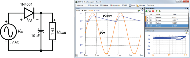
Figure 4-11: Circuit and behavior of a 1N4001 diode with a 5 V AC supply, 1 kΩ load, and parallel 10 μF capacitor
Capacitors use a dielectric material, such as ceramic, glass, paper, or plastic, to insulate the two charged plates. Two common capacitor types are ceramic and electrolytic capacitors. Ceramic capacitors are small and low cost and degrade over time. Electrolytic capacitors can store much larger amounts of energy but also degrade over time. Glass, mica, and tantalum capacitors tend to be more reliable but are considerably more expensive.
Figure 4-12 illustrates a 100 nF (0.1 μF) ceramic capacitor and a 47 μF electrolytic capacitor. Note that the electrolytic capacitor is polarized, with the negative lead marked on the capacitor surface with a band; like the LED, the negative lead is shorter than the positive lead.
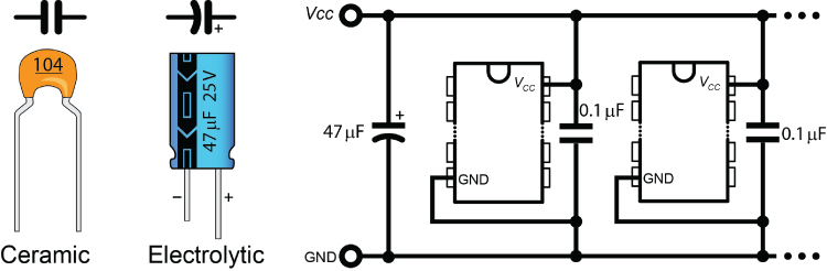
Figure 4-12: Ceramic (nonpolarized) and electrolytic (polarized) capacitors and an example decoupling circuit
The numbering for capacitors is reasonably straightforward; unfortunately, on ceramic capacitors it can be small and hard to read.
- The first number is the first digit of the capacitor value.
- The second number is the second digit of the capacitor value.
- The third number is the number of zeroes, where the capacitor value is in pF (picofarads).
- Additional letters represent the tolerance and voltage rating of the capacitor but can be ignored for the moment.
Therefore, for example:
- 104 = 100000 pF = 100 nF = 0.1 μF
- 102 = 1,000 pF = 1 nF
- 472 = 4,700 pF = 4.7 nF
The voltage regulator circuit presented earlier (refer to Figure 4-7) used two capacitors to smooth out the ripples in the supply by charging and discharging in opposition to those ripples. Capacitors can also be used for a related function known as decoupling.
Coupling is often an undesirable relationship that occurs between two parts of a circuit due to the sharing of power supply connections. This relationship means that if there is a sudden high power demand by one part of the circuit, then the supply voltage will drop slightly, affecting the supply voltages of other parts of the circuit. ICs impart a variable load on the power supply lines—in fact, a load that can change quickly causes a high-frequency voltage variation on the supply lines to other ICs. As the number of ICs in the circuit increases, the problem will be compounded.
Small capacitors, known as decoupling capacitors, can act as a store of energy that removes the noise signals that may be present on your supply lines as a result of these IC load variations. An example circuit is illustrated in Figure 4-12, where the larger 47 μF capacitor filters out lower-frequency variations and the 0.1 μF capacitors filter out higher-frequency noise. Ideally the leads on the 0.1 μF capacitors should be as short as possible to avoid producing undesirable effects (relating to inductance) that will limit it from filtering the highest-level frequencies. Even the surface-mounted capacitors used on the Beagle boards to decouple the ball grid array (BGA) pins on the AM335x produce a small inductance of about 1–2 nH. As a result, one 0.1 μF capacitor is recommended for every two power balls, and the traces (board tracks) have to be as “short as humanly possible” (Texas Instruments, 2011). See tiny.cc/beagle402 for a full guide.
Transistors
Transistors are one of the core ingredients of the AM335x microprocessor, and indeed almost every other electronic system. Simply put, their function can be to amplify a signal or to turn a signal on or off, whichever is required. The Beagle board GPIOs can handle only modest currents, so we need transistors to help us when interfacing them to electronic circuits that require larger currents to operate.
Bipolar junction transistors (BJTs), usually just called transistors, are formed by adding another doped layer to a pn-junction diode to form either a p-n-p or an n-p-n transistor. There are other types of transistors, such as field effect transistors (FETs), which are discussed shortly. The name bipolar comes from the fact that the current is carried by both electrons and holes. They have three terminals, with the third terminal connected to the middle layer in the sandwich, which is very narrow, as illustrated in Figure 4-13.
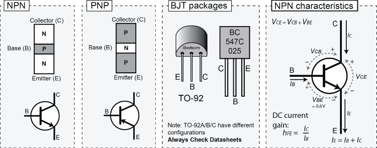
Figure 4-13: Bipolar junction transistors (BJTs)
Figure 4-13 presents quite an amount of information about transistors, including the naming of the terminals as the base (B), collector (C), and emitter (E). Despite there being two main types of BJT transistor (NPN and PNP), the NPN transistor is the most commonly used. In fact, any transistor examples in this chapter use a single BC547 NPN transistor type.
The BC547 is a 45 V, 100 mA general-purpose transistor that is commonly available, is low cost, and is provided in a leaded TO-92 package. The identification of the legs in the BC547 is provided in Figure 4-13, but please be aware that this order is not consistent with all transistors—always check the datasheet! The maximum VCE (aka VCEO ) is 45 V, and the maximum collector current (IC ) is 100 mA for the BC547. It has a typical DC current gain (hFE ) of between 180 and 520, depending on the group used (e.g., A, B, C). Those characteristics are explained in the next sections.
Transistors as Switches
Let's examine the characteristics for the NPN transistor as illustrated in Figure 4-13 (on the rightmost diagram). If the base-emitter junction is forward biased and a small current is entering the base (IB
), the behavior of a transistor is such that a proportional but much larger current (![]() ) will be allowed to flow into the collector terminal, as hFE
will be a value of 180 to 520 for a transistor such as the BC547. Because IB
is much smaller than IC
, you can also assume that IE
is approximately equal to IC
.
) will be allowed to flow into the collector terminal, as hFE
will be a value of 180 to 520 for a transistor such as the BC547. Because IB
is much smaller than IC
, you can also assume that IE
is approximately equal to IC
.
Figure 4-14 illustrates the example of a BJT being used as a switch. In part (a) the voltage levels have been chosen to match those available on the Beagle boards. The resistor on the base is chosen to have a value of 2.2 kΩ so that the base current will be small (![]() , which is about 1.2 mA). The resistor on the collector is small, so the collector current will be reasonably large (
, which is about 1.2 mA). The resistor on the collector is small, so the collector current will be reasonably large (![]() ).
).
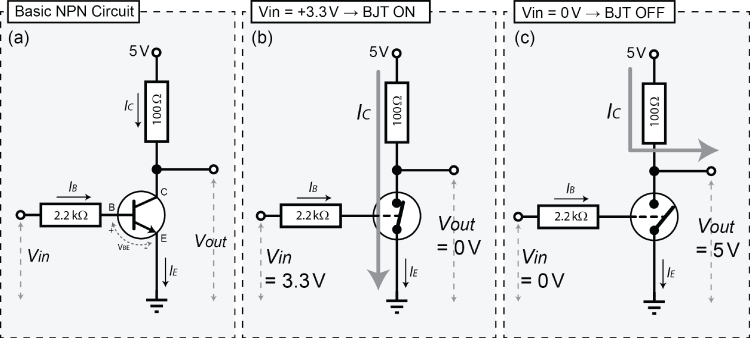
Figure 4-14: The BJT as a switch
Figure 4-14(b) illustrates what happens when an input voltage of 3.3 V is applied to the base terminal. The small base current causes the transistor to behave like a closed switch (with a very low resistance) between the collector and the emitter. This means that the voltage drop across the collector-emitter will be almost zero, and all of the voltage is dropped across the 100 Ω load resistor, causing a current to flow directly to ground through the emitter. The transistor is saturated because it cannot pass any further current. Because there is almost no voltage drop across the collector-emitter, the output voltage, Vout , will be almost 0 V.
Figure 4-14(c) illustrates what happens when the input voltage Vin = 0 V is applied to the base terminal and there is no base current. The transistor behaves like an open switch (very large resistance). No current can flow through the collector-emitter junction, as this current is always a multiple of the base current and the base current is zero; therefore, almost all of the voltage is dropped across the collector-emitter. In this case the output, Vout , can be up to +5 V (though as implied by the illustrated flow of IC through the output terminal, the exact value of Vout depends on the size of IC , as any current flowing through the 100 Ω resistor will cause a voltage drop across it).
Therefore, the switch behaves somewhat like an inverter. If the input voltage is 0 V, the output voltage is +5 V, and if the input voltage is +3.3 V, the output voltage will be 0 V. You can see the actual measured values of this circuit in Figure 4-15, when the input voltage of 3.3 V is applied to the base terminal. In this case, the Analog Discovery Waveform Generator is used to output a 1 kHz square wave, with an amplitude of 1.65 V and an offset of +1.65 V (forming a 0 V to 3.3 V square wave signal), so it appears like a 3.3 V source turning on and then off, 1,000 times per second. All the measurements in this figure were captured with the input at 3.3 V. The base-emitter junction is forward biased, and just like the diode before, this will have a forward voltage of about 0.7 V. The actual voltage drop across the base-emitter is 0.83 V, so the voltage drop across the base resistor will be 2.440 V. The actual base current is 1.1 mA (![]() ). This current turns on the transistor, placing the transistor in saturation, so the voltage drop across the collector-emitter is very small (measured at 0.2 V). Therefore, the collector current is 49.8 mA (
). This current turns on the transistor, placing the transistor in saturation, so the voltage drop across the collector-emitter is very small (measured at 0.2 V). Therefore, the collector current is 49.8 mA (![]() ). To choose an appropriate base resistor to place the BJT deep in saturation, use the following practical formula:
). To choose an appropriate base resistor to place the BJT deep in saturation, use the following practical formula:
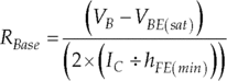
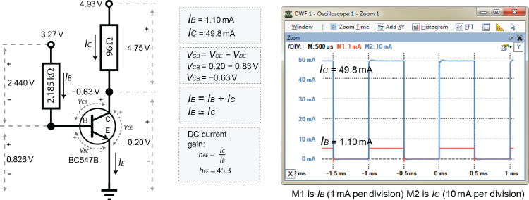
Figure 4-15: Realization of the transistor as a switch (saturation) and confirmation that all relationships hold true1
For the case of a base supply of 3.3 V, with a collector current of 50 mA and a minimum gain hFE(min)
of 100, ![]() .
.
You can find all of these values in the transistor's datasheet. VBE(sat) is typically provided on a plot of VBE versus IC at room temperature, where we require IC to be 50 mA. The value of VBE(sat) is between 0.6 V and 0.95 V for the BC547, depending on the collector current and the room temperature. The resistor value is further divided by two to ensure that the transistor is placed deep in the saturation region (maximizing IC ). Therefore, in this case a 2.2 kΩ resistor is used, as it is the closest generally available nominal value.
Why should you care about this with the Beagle boards? Well, because the boards can only source or sink very small currents from its GPIO pins, you can connect the GPIO pin to the base of a transistor so that a small current entering the base of the transistor can switch on a much larger current, with a much greater voltage range. Remember that in the example in Figure 4-15, a current of 1.1 mA is able to switch on a large current of 49.8 mA (45 times larger, but still lower than the 100 mA limit of the BC547). Using this transistor arrangement with a Beagle board will allow a 5 mA current at 3.3 V from a GPIO to safely drive a 100 mA current at up to 45 V by choosing suitable resistor values.
One constraint in using transistors to drive a circuit is that they have a maximum switching frequency. If you increase the frequency of the input signal to the circuit in Figure 4-16 to 500 kHz, the output is distorted, though it is still switching from low to high. However, increasing this to 1 MHz means that the controlled circuit never switches off.
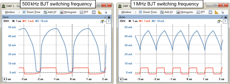
Figure 4-16: Frequency response of the BJT circuit (frequency is 500 kHz and 1 MHz)
Field Effect Transistors as Switches
A simpler alternative to using BJTs as switches is to use field effect transistors (FETs). FETs are different from BJTs in that the flow of current in the load circuit is controlled by the voltage, rather than the current, on the controlling input. Therefore, it is said that FETs are voltage-controlled devices and BJTs are current-controlled devices. The controlling input for a FET is called the gate (G), and the controlled current flows between the drain (D) and the source (S).
Figure 4-17 illustrates how you can use an n-channel FET as a switch. Unlike the BJT, the resistor on the controlling circuit (1 MΩ) is connected from the input to GND, meaning that a very small current (I = V/R) will flow to GND, but the voltage at the gate will be the same as the Vin voltage. A significant advantage of FETs is that almost no current flows into the gate control input. However, the voltage on the gate is what turns on and off the controlled current, ID , which flows from the drain to the source in this example.
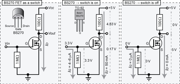
Figure 4-17: The field effect transistor as a switch
When the input voltage is high (3.3 V), the drain-source current will flow (ID = 50 mA), so the voltage at the output terminal will be 0.17 V, but when the input voltage is low (0 V), no drain-source current will flow. Just like the BJT, if you were to measure the voltage at the drain terminal, the output voltage (Vout ) would be high when the input voltage is low, and the output voltage would be low when the input voltage is high, though again the actual value of the “high” output voltage depends on the current drawn by the succeeding circuit.
The Fairchild Semiconductor BS270 N-Channel Enhancement Mode FET is a low-cost device (~$0.10) in a TO-92 package that is capable of supplying a continuous drain current (ID ) of up to 400 mA at a drain-source voltage of up to 60 V. However, at a gate voltage (VG ) of 3.3 V the BS270 can switch a maximum drain current of approximately 130 mA. This makes it ideal for use with the Beagle boards, as the GPIO voltages are in range and the current required to switch on the FET is about 3 μA–6 μA depending on the gate resistor chosen. One other feature of using a FET as a switch is that it can cope with much higher switching frequencies, as shown in Figure 4-18. Remember that in Figure 4-16 the BJT switching waveform is very distorted at 1 MHz. It should be clear from Figure 4-18 that the FET circuit is capable of dealing with much higher switching frequencies than the BJT circuit.
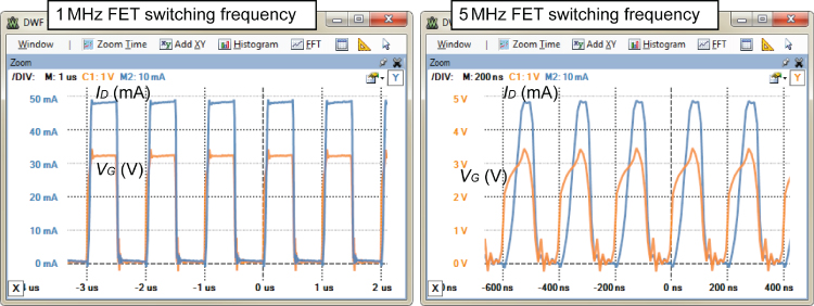
Figure 4-18: Frequency response of the FET circuit as the switching frequency is set at 1 MHz and 5 MHz
The BS270 also has a high-current diode that is used to protect the gate from the type of reverse inductive voltage surges that could arise if the FET were driving a DC motor.
As mentioned, one slight disadvantage of the BS270 is that it can only switch a maximum drain current of approximately 130 mA at a gate voltage of 3.3 V. However, the high input impedance of the gate means that you can use two (or indeed more) BS270s in parallel to double the maximum current to approximately 260 mA at the same gate voltage. Also, the BS270 can be used as a gate driver for Power FETs, which can switch much larger currents.
Optocouplers/Optoisolators
Optocouplers (or optoisolators) are small, low-cost digital switching devices that are used to isolate two electrical circuits from each other. This can be important for your Beagle board circuits if you have a concern that a design problem with a connected circuit could possibly source or sink a large current from/to your board. They are available in low-cost (~$0.15) four-pin DIP form.
An optocoupler uses an LED emitter that is placed close to a photodetector transistor, separated by an insulating film within a silicone dome. When a current (If ) flows through the LED emitter legs, the light that falls on the photodetector transistor from the LED allows a separate current (Ic ) to flow through the collector-emitter legs of the photo detector transistor (see Figure 4-19). When the LED emitter is off, no light falls on the photo detector transistor, and there will be almost no collector emitter current (Ic ). There is no electrical connection between one side of the package and the other, as the signal is transmitted only by light, providing electrical isolation for up to 5,300 VRMS for an optocoupler such as the SFH617A. You can even use PWM with optocouplers, as it is a binary on/off signal.
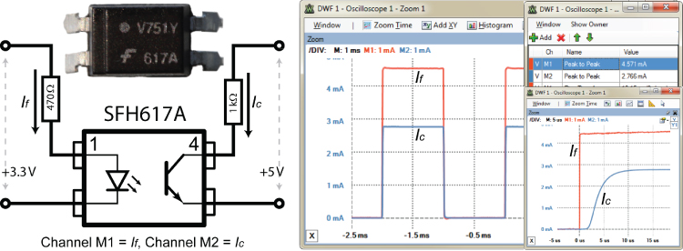
Figure 4-19: Optocoupler (617A) circuit with the captured input and output characteristics
Figure 4-19 illustrates an example optocoupler circuit and the resulting oscilloscope traces for the resistor and voltage values chosen. These values were chosen to be consistent with those that you might use with the Beagle boards. The resistor value of 470 Ω was chosen to allow the 3.3 V output to drive a forward current If
of about 4.5 mA through the LED emitter. From Figure 4 in the datasheet,2 this results in a forward voltage of about 1.15 V across the diode); ![]() Therefore, the circuit was built using the closest nominal value of 470 Ω.
Therefore, the circuit was built using the closest nominal value of 470 Ω.
The oscilloscope is displaying current by using the differential inputs of the Analog Discovery to measure the voltage across the known resistor values and using two mathematical channels to divide by the resistance values. In Figure 4-19 you can see that If
is 4.571 mA and that Ic
is 2.766 mA. The proportionality of the difference is the current transfer ratio (CTR), and it varies according to the level of If
and the operating temperature. Therefore, the current transfer at 4.571 mA is 60.5 percent (![]() ), which is consistent with the datasheet. The rise time and fall time are also consistent with the values in the datasheet of tr
= 4.6 µs and tf
= 15 µs. These values limit the switching frequency. Also, if it is important to your circuit that you achieve a high CTR, there are optocouplers with built-in Darlington transistor configurations that result in CTRs of up to 2,000 percent (e.g., the 6N138 or HCPL2730). Finally, there are high-linearity analog optocouplers available (e.g., the HCNR200 from Avago) that can be used to optically isolate analog signals.
), which is consistent with the datasheet. The rise time and fall time are also consistent with the values in the datasheet of tr
= 4.6 µs and tf
= 15 µs. These values limit the switching frequency. Also, if it is important to your circuit that you achieve a high CTR, there are optocouplers with built-in Darlington transistor configurations that result in CTRs of up to 2,000 percent (e.g., the 6N138 or HCPL2730). Finally, there are high-linearity analog optocouplers available (e.g., the HCNR200 from Avago) that can be used to optically isolate analog signals.
Switches and Buttons
Other components with which you are likely to need to work with are switches and buttons. They come in many different forms: toggle, push button, selector, proximity, joystick, reed, pressure, temperature, etc. However, they all work under the same binary principles of either interrupting the flow of current (open) or enabling the flow of current (closed). Figure 4-20 illustrates several different common switch types and outlines their general connectivity.
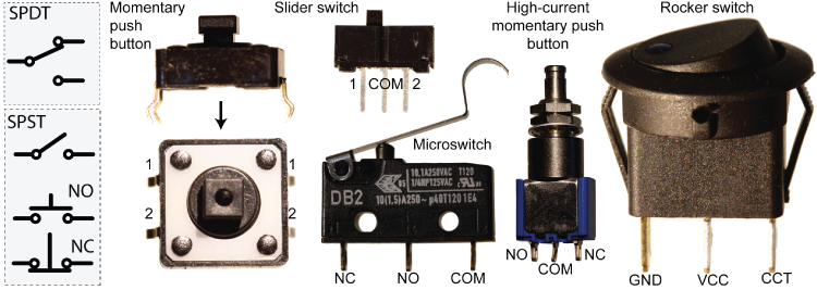
Figure 4-20: Various switches and configurations
Momentary push button switches (SPST—single pole, single throw) like the one illustrated in Figure 4-20 are either normally open (NO) or normally closed (NC). NO means you have to activate the switch to allow current to flow, whereas NC means that when you activate the button, current does not flow. For the particular push button illustrated, both pins 1 and both pins 2 are always connected, and for the duration of time you press the button, all four pins are connected together. Looking at slider switches (SPDT—single pole, double throw), the common connection (COM) is connected to either 1 or 2 depending on the slider position. In the case of microswitches and the high-current push button, the COM pin is connected to NC if the switch is pressed and is connected to NO if the switch is depressed. Finally, the rocker switch illustrated often has an LED that lights when the switch is closed, connecting the power (VCC) leg to the circuit (CCT) leg.
All of these switch types suffer from mechanical switch bounce, which can be extremely problematic when interfacing to microprocessors like the Beagle boards. Switches are mechanical devices and when they are pressed, the force of contact causes the switch to repeatedly bounce from the contact on impact. It only bounces for a small duration (typically milliseconds), but the duration is sufficient for the switch to apply a sequence of inputs to a microprocessor.
Figure 4-21(a) illustrates the problem in action using the rising/falling-edge trigger condition of the Analog Discovery oscilloscope. A momentary push button is placed in a simple series circuit with a 10 kΩ resistor, and the voltage is measured across the resistor. When the switch hits the contact, the output is suddenly high, but the switch then bounces back from the contact, and the voltage falls down again. After about 2 ms–3 ms (or longer), it has almost fully settled. Unfortunately, this small bounce can lead to false inputs to a digital circuit. For example, if the threshold were 3 V, this may be read in as 101010101, rather than a more correct value of 000001111.
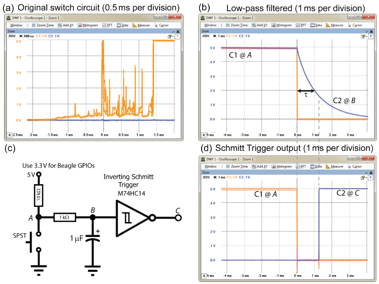
Figure 4-21: (a) Switch bouncing with no components other than the switch and 10 kΩ resistor; (b) low-pass filtered output at point B; (c) a Schmitt trigger circuit; and, (d) output of the Schmitt trigger circuit at point C, versus the input at point A
There are a number of ways to deal with switch bounce in microprocessor interfacing:
A low-pass filter can be added in the form of a resistor-capacitor circuit, as illustrated in Figure 4-21(c) using a 1 μF capacitor. Unfortunately, this leads to delay in the input. If you examine the time base, it takes about 2 ms before the input reaches 1 V. Also, bounce conditions can delay this further. These values are chosen using the RC time constant ![]() , so
, so ![]() , which is the time taken to charge a capacitor to ~63.2% or discharge it to ~36.8%. This value is marked on Figure 4-21(b) at approximately 1.9 V.
, which is the time taken to charge a capacitor to ~63.2% or discharge it to ~36.8%. This value is marked on Figure 4-21(b) at approximately 1.9 V.
- Software may be written so that after a rising edge occurs, it delays a few milliseconds and then reads the “real” state.
- For slider switches (SPDT), an SR-latch can be used.
- For momentary push button switches (SPSTs), a Schmitt trigger (74HC14N), which is discussed in the next section, can be used with an RC low-pass filter as in Figure 4-21(c).
Hysteresis
Hysteresis is designed into electronic circuits to avoid rapid switching, which would wear out circuits. A Schmitt trigger exhibits hysteresis, which means that its output is dependent on the present input and the history of previous inputs. This can be explained with an example of an oven baking a cake at 350 degrees Fahrenheit.
- Without hysteresis: The element would heat the oven to 350°F. Once 350°F is achieved, the element would switch off. It would cool below 350°F, and the element would switch on again. Rapid switching!
- With hysteresis: The circuit would be designed to heat the oven to 360°F, and at that point the element would switch off. The oven would cool, but it is not designed to switch back on until it reaches 340°F. The switching would not be rapid, protecting the oven, but there would be a greater variation in the baking temperature.
With an oven that is designed to have hysteresis, is the element on or off at 350°F? That depends on the history of inputs—it is on if the oven is heating; it is off if the oven is cooling.
The Schmitt trigger in Figure 4-21(c) exhibits the same type of behavior. The VT+ for the M74HC14 Schmitt trigger is 2.9 V, and the VT− is 0.93 V when running at a 5 V input, which means a rising input voltage has to reach 2.9 V before the output changes high, and a falling input voltage has to drop to 0.93 V before the output changes low. Any bounce in the signal within this range is simply ignored. The low-pass filter reduces the possibility of high-frequency bounces. The response is presented in Figure 4-21(d). Note that the time base is 1 ms per division, illustrating how “clean” the output signal is. The configuration uses a pull-up resistor, the need for which is discussed shortly.
Logic Gates
Boolean algebra functions have only two possible outcomes, either true or false, which makes them ideal for developing a framework to describe electronic circuits that are either on or off (high or low). Logic gates perform these Boolean algebra functions and operations, forming the basis of the functionality inside modern microprocessors, such as the AM335x. Boolean values are not the same as binary numbers. (Binary numbers are a base 2 representation of whole and fractional numbers, whereas Boolean refers to a data type that has only two possible values, either true or false.)
It is often the case that you will need to interface to different types of logic gates and systems using the Beagle board GPIOs to perform an operation such as gating an input or sending data to a shift register. Logic gates fall into two main categories:
- Combinational logic: The current output is dependent on the current inputs only (e.g., AND, OR, decoders, multiplexers, etc.).
- Sequential logic: The current output is dependent on the current inputs and previous inputs. They can be said to have different states, and what happens with a given input depends on what state they are in (e.g., latches, flip-flops, memory, counters, etc.).
Combinational logic circuits will provide the same output for the same set of inputs, regardless of the order in which the inputs are applied. Figure 4-22 illustrates the core combinational logic gates with their logic symbols, truth tables, and IC numbers. The truth table provides the output that you will get from the gate on applying the listed inputs.
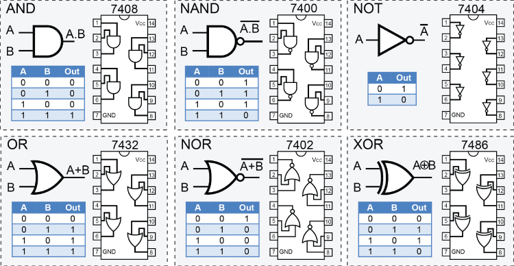
Figure 4-22: General logic gates
ICs have a number that describes their manufacturer, function, logic family, and package type. For example, the MM74HC08N in Figure 4-23(a) has a manufacturer code of MM (Fairchild Semiconductor), is a 7408 (quad two-input AND gates), is of the HC (CMOS) logic family, and is in an N (plastic dual in-line package) form.
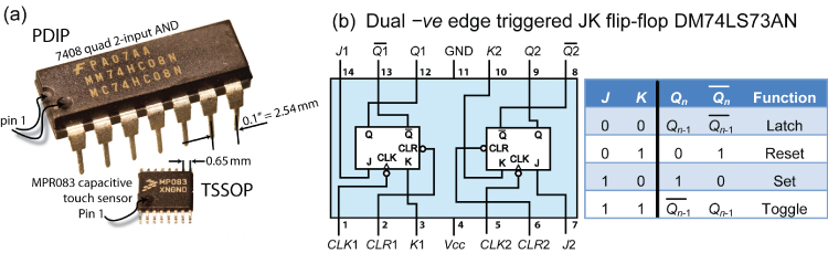
Figure 4-23: (a) IC package examples (to scale), and (b) the JK flip-flop
ICs are available in different package types. Figure 4-23(a) shows to scale a PDIP (plastic dual in-line package) and a small outline package TSSOP (thin shrink small outline package). There are many types: surface mount, flat package, small outline package, chip-scale package, and ball grid array (BGA). You have to be careful when ordering ICs that you have the capability to use them. DIP/PDIP ICs have perfect forms for prototyping on breadboards as they have a 0.1" leg spacing. There are adapter boards available for converting small outline packages to 0.1" leg spacing. Unfortunately, BGA ICs, such as the AM335x SoC and the OSD3358 SiP, require sophisticated equipment for soldering.
The family of currently available ICs is usually transistor-transistor logic (TTL) (with Low-power Schottky (LS)) or some form of complementary metal-oxide-semiconductor (CMOS). Table 4-1 compares these two families of 7408 ICs using their respective datasheets. The propagation delay is the longest delay between an input changing value and the output changing value for all possible inputs to a logic gate. This delay limits the logic gate's speed of operation.
Table 4-1: Comparison of Two Commercially Available TTL and CMOS ICs for a 7408 Quadruple Two-input AND gates IC
| CHARACTERISTIC | SN74LS08N | SN74HC08N |
| Family |
Texas TTL PDIP Low-power Schottky (LS) |
Texas CMOS PDIP High-speed CMOS (HC) |
| VCC supply voltage | 4.5 V to 5.5 V (5 V typical) | 2 V to 6 V |
| VIH high-level input voltage | min 2 V | VCC at 5 V min = 3.5 V |
| VIL low-level input voltage | max 0.8 V | VCC at 5 V max = 1.5 V |
| Time propagation delay (TPD ) | Typical 12 ns (↑) 17.5 ns (↓) | Typical 8 ns (↑↓) |
| Power (at 5 V) | 5 mW (max) | 0.1 mW (max) |
Figure 4-24 illustrates the acceptable input and output voltage levels for both TTL and CMOS logic gates when VDD = 5 V. The noise margin is the absolute difference between the output voltage levels and the input voltage levels. This noise margin ensures that if the output of one logic gate is connected to the input of a second logic gate, that noise will not affect the input state. The CMOS logic family input logic levels are dependent on the supply voltage, VDD , where the high-level threshold is 0.7 × VDD , and the low-level threshold is 0.3 × VDD . It should be clear from Figure 4-24 that there are differences in behavior. For example, if the input voltage were 2.5 V, then the TTL gate would perceive a logic high level, but the CMOS gate (at 5 V) would perceive an undefined level. Also, the output of a CMOS gate, with VDD = 3.3 V, would provide sufficient output voltage to trigger a logic high input on a TTL gate, but would not on a CMOS gate with VDD = 5.0 V.
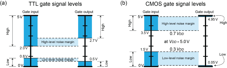
Figure 4-24: Gate signal levels on the input and output of logic gates (a) TTL, and (b) CMOS at 5 V
High-Speed CMOS (HC) can support a wide range of voltage levels, including the Beagle board's 3.3 V input/outputs. The GND label is commonly used to indicate the ground supply voltage, where VEE is often used for BJT-based devices and VSS for FET-based devices. Traditionally, VCC was used as the label for the positive supply voltage on BJT-based devices and VDD for FET-based devices; however, it is now common to see VCC being used for both.
Figure 4-23(b) illustrates a sequential logic circuit, called a JK flip-flop. JK flip-flops are core building blocks in circuits such as counters. These differ from combinational logic circuits in that the current state is dependent on the current inputs and the previous state. You can see from the truth table that if J = 0 and K = 0 for the input, then the value of the output Qn will be the output value that it was at the previous time step (it behaves like a one-bit memory). A time step is defined by the clock input (CLK), which is a square wave synchronizing signal. The same type of timing signal is present on the Beagle boards—it is the clock frequency, and a 1 GHz clock goes through up to 1,000,000,000 square wave cycles per second!
Floating Inputs
One common mistake when working with digital logic circuits is to leave unused logic gate inputs “floating,” or disconnected. The family of the chip has a large impact on the outcome of this mistake. With the TTL logic families these inputs will “float” high and can be reasonably expected to be seen as logic-high inputs. With TTL ICs it is good practice to “tie” (i.e., connect) the inputs to ground or the supply voltage, so that there is absolutely no doubt about the logic level being asserted on the input at all times.
With CMOS circuits the inputs are very sensitive to the high voltages that can result from static electricity and electrical noise and should also never be left floating. Figure 4-25 gives the likely output of an AND gate that is wired as shown in the figure. The correct outcome is displayed in the “Required (A.B)” column.
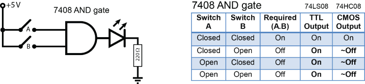
Figure 4-25: An AND gate with the inputs accidentally left floating when the switches are open
Unused CMOS inputs that are left floating (between VDD and GND) can gradually charge up because of leakage current and, depending on the IC design, could provide false inputs or waste power by causing a DC current to flow (from VDD to GND). To solve this problem you can use pull-up or pull-down resistors, depending on the desired input state (these are ordinary resistors with suitable values—it's their role that is “pull up” or “pull down”), which are described in the next section.
Pull-Up and Pull-Down Resistors
To avoid floating inputs, you can use pull-up or pull-down resistors as illustrated in Figure 4-26. Pull-down resistors are used if you want to guarantee that the inputs to the gate are low when the switches are open, and pull-up resistors are used if you want to guarantee that the inputs are high when the switches are open.
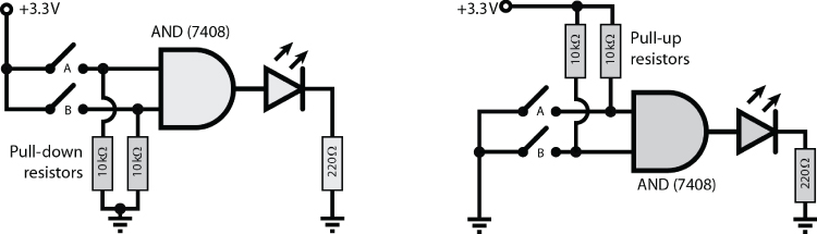
Figure 4-26: Pull-down and pull-up resistors, used to ensure that the switches do not create floating inputs
The resistors are important because when the switch is closed, the switch would form a short circuit to ground if they were omitted and replaced by lengths of wire. The size of the pull-down/up resistors is also important; their value has to be low enough to solidly pull the input low/high when the switches are open but high enough to prevent too much current flowing when the switches are closed. Ideal logic gates have infinite impedance and any resistor value (short of infinite) would suffice. However, real logic gates leak current, and you have to overcome this leakage. To minimize power consumption, you should choose the maximum value that actually pulls the input low/high. A 3.3 kΩ–10 kΩ resistor will usually work perfectly, but 3.3 V will drive 1 mA–0.33 mA through them respectively and dissipate 3.3 mW–1 mW of power respectively when the switch is closed. For power-sensitive applications you could test larger resistors of 50 kΩ or greater.
The Beagle boards have weak internal pull-up and pull-down resistors that can be used for this purpose. This is discussed in Chapter 6. One other issue is that inputs will have some stray capacitance to ground. Adding a resistor to the input creates an RC low-pass filter on the input signal that can delay input signals. That is not important for manually pressed buttons, as the delay will be on the order of 0.1 µs for the preceding example, but it could affect the speed of digital communication bus lines.
Open-Collector and Open-Drain Outputs
To this point in the chapter, all of the ICs have a regular output, where it is driven close to GND or the supply voltage of the IC (VCC ). If you are connecting to another IC or component that uses the same voltage level, then that should be fine. However, if the first IC had a supply voltage of 3.3 V and you needed to drive the output into an IC that had a supply voltage of 5 V, then you may need to perform level shifting.
Many ICs are available in a form with open-collector outputs, which are particularly useful for interfacing between different logic families and for level shifting. This is because the output is not at a specific voltage level, but rather attached to the base input of an NPN transistor that is inside the IC. The output of the IC is the “open” collector of the transistor, and the emitter of the transistor is tied to the IC's GND. It is possible to use a FET (74HC03) instead of a BJT (74LS01) inside the IC, and while the concept is the same, it is called an open-drain output. Figure 4-27 illustrates this concept and provides an example circuit using a 74HC03 (quad, two-input NAND gates with open-drain outputs) to drive a 5 V circuit. The advantage of the open-drain configuration is that CMOS ICs support the 3.3 V level available on the Beagle board's GPIOs. Essentially, the drain resistor that is used in Figure 4-17 is placed outside the IC package, as illustrated in Figure 4-27, and it has a value of 10 kΩ in this case.
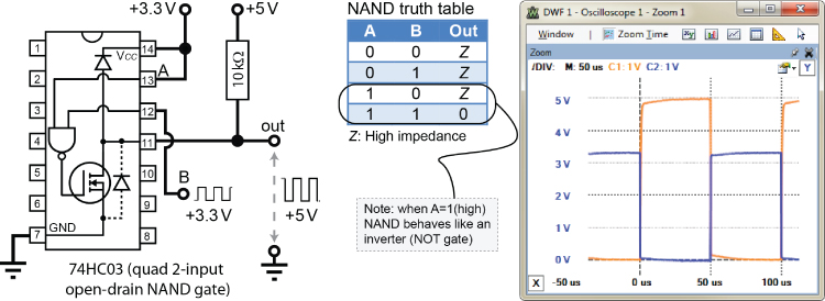
Figure 4-27: Open-drain level-shifting example
Interestingly, a NAND gate with one input tied high (or the two inputs tied together) behaves like a NOT gate. In fact, NAND or NOR gates, each on its own, can replicate the functionality of any of the logic gates, and for that reason they are called universal gates.
Open-collector outputs are often used to connect multiple devices to a bus. You will see this in Chapter 8 when the Beagle board's I2C buses are described. When you examine the truth table in the datasheet of an IC, such as the 74HC03, you will see the letter Z used to represent the output (as in Figure 4-27). This means it is a high-impedance output, and the external pull-up resistor can pull the output to the high state.
Interconnecting Gates
To create useful circuits, logic gates are interconnected to other logic gates and components. It is important to understand that there are limits to the interconnect capabilities of gates.
The first limit is the capability of the logic gate to source or sink current. When the output of a gate is logic high, it acts as a current source, providing current for connected logic gates or the LEDs shown in Figure 4-26. If the output of the gate is logic low, the gate acts as a current sink, whereby current flows into the output. Figure 4-28(a) demonstrates this by placing a current-limiting resistor and an LED between VCC and the output of the logic gate, with the LED cathode connected to the logic gate output. When the output of the gate is high, there is no potential difference, and the LED will be off; but when the output is low, a potential difference is created, and current will flow through the LED and be sinked by the output of the logic gate. According to the datasheet of the 74HC08, it has an output current limit (IO ) of ±25 mA, meaning that it can source or sink 25 mA. Exceeding these values will damage the IC.
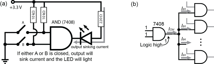
Figure 4-28: (a) Sinking current on the output, and (b) TTL fan-out example
It is often necessary to connect the output of a single (driving) gate to the input of several other gates. Each of the connected gates will draw a current, thus limiting the total number of connected gates. The fan-out is the number of gates that are connected to the output of the driving gate. As illustrated in Figure 4-28(b), for TTL the maximum fan-out depends on the output (IO ) and input current (II ) requirement values when the state is low (= IOL(max)/IIL(max) ) and the state is high (= IOH(max)/IIH(max) ). Choose the lower value, which is commonly 10 or greater. The fan-in of an IC is the number of inputs that it has. For the 7408 they are two-input AND gates, so they have a fan-in of 2.
CMOS gate inputs have extremely large resistance and draw almost no current, allowing for large fan-out capability (>50); however, each input adds a small capacitance (CL
≈ 3–10 pF) that must be charged and discharged by the output of the previous stage. The greater the fan-out, the greater the capacitive load on the driving gate, which lengthens the propagation delay. For example, the 74HC08 has a propagation delay (tpd
) of about 11 ns and an input capacitance (CI
) of 3.5 pF (assuming for this example that this leads to tpd = RC = 3.5 ns per connection). If one 78HC08 were driving 10 other similar gates and each added 3.5 ns of delay, then the propagation delay would increase to ![]() ns of delay, reducing the maximum operating frequency from 91 MHz to 22 MHz.
ns of delay, reducing the maximum operating frequency from 91 MHz to 22 MHz.
Analog-to-Digital Conversion
The Beagle boards have several analog-to-digital converter (ADC) inputs that can be used to take an analog signal and create a digital representation of this signal. This enables us to connect many different types of sensors, such as distance sensors, temperature sensors, light-level sensors, and so on. However, you have to be careful with these inputs, as they should not source or sink current, because the analog outputs of the sensors are likely to be very sensitive to any additional load in parallel with the output. To solve this problem you need to first look at how operational amplifiers function.
Analog signals are continuous signals that represent the measurement of some physical phenomenon. For example, a microphone is an analog device, generally known as a transducer, which can be used to convert sound waves into an electrical signal that, for example, varies between −5 V and +5 V depending on the amplitude of the sound wave. Analog signals use a continuous range of values to represent information, but if you want to process that signal using your Beagle board, then you need a discrete digital representation of the signal. This is one that is sampled at discrete instants in time and subsequently quantized to discrete values of voltage, or current. For example, audio signals will vary over time; so to sample a transducer signal to digitally capture human speech (e.g., speech recognition), you need be cognizant of two factors:
- Sampling rate: Defines how often you are going to sample the signal. Clearly, if you create a discrete digital sample by sampling the voltage every one second, the speech will be indecipherable.
- Sampling resolution: Defines the number of digital representations that you have to represent the voltage at the point in time when the signal is sampled. Clearly, if you had only one bit, you could capture only if the signal were closer to +5 V or −5 V, and again the speech signal would be indecipherable.
Sampling Rate
Representing a continuous signal perfectly in a discrete form requires an infinite amount of digital data. Fortunately, there are limits to how well human hearing performs, and therefore we can place limits on the amount of data to be discretized. For example, 44.1 kHz and 48 kHz are common digital audio sampling rates for encoding MP3 files, which means that if you use the former, you will have to store 44,100 samples of your transducer voltage every second. The sample rate is generally determined by the need to preserve a certain frequency content of the signal. For example, humans (particularly children) can hear audio signals at frequencies from about 20 Hz up to about 20 kHz. Nyquist's sampling theorem states that the sampling frequency must be at least twice the highest frequency component present in the signal. Therefore, if you want to sample audio signals, you need to use a sampling rate of at least twice 20 kHz, which is 40 kHz, which helps explain the magnitude of the sampling rates used in encoding MP3 audio files (typically 44,100 samples per second—that is, 44.1 kS/s).
Quantization
The Beagle boards have several 12-bit ADC inputs that work in the range of 0–1.8 V, which means that there are 212 = 4,096 possible discrete representations (numbers) for this sampling resolution. If the voltage is exactly 0 V, we can use the decimal number 0 to represent it. If the voltage is exactly 1.8 V, we can use the number 4,095 to represent it. So, what voltage does the decimal number 1 represent? It is ![]() . Therefore, each decimal number between 0 and 4,095 (4,096 values) represents a step of about 0.44 mV.
. Therefore, each decimal number between 0 and 4,095 (4,096 values) represents a step of about 0.44 mV.
The preceding audio sampling example also illustrates one of the challenges you face with the Beagle board configurations. If the sensor outputs a voltage of −5 to +5 V, or more commonly 0 V to +5 V, you need to alter that range to be between 0 and 1.8 V to be compatible with the ADC. In Chapter 6, you'll look at how you can solve this problem. A second and more complex problem is that we must not source or sink current from/to the Beagle board's ADC circuitry, and to solve that we need to introduce a powerful concept that predates the digital computer, called the operational amplifier.
Operational Amplifiers
Operational amplifiers (op-amps) are composed from many BJTs or FETs within the one IC (e.g., the LM741). They can be used to create several useful circuits, one of which you will need in Chapter 9 to correctly interface to analog sensors.
Ideal Operational Amplifiers
Figure 4-29(a) illustrates an ideal op-amp, placed in a basic circuit with no feedback (aka open-loop). The op-amp has two inputs, a noninverting input (+) and an inverting input (−), and it produces an output that is proportional to the difference between them, i.e., Vout = G(V1 − V2), where V1 and V2 are the voltage levels on these two inputs, respectively. Some of the characteristics of an ideal op-amp include the following:
- An infinite open-loop gain, G
- An infinite input impedance
- A zero output impedance
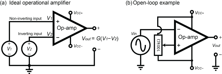
Figure 4-29: (a) The ideal op-amp, and (b) an open-loop comparator example
No real-world op-amp has an infinite open-loop gain, but voltage gains of 200,000 to 30,000,000 are commonplace. Such a gain can be treated as infinite, which means in theory that even a small difference between the inputs would lead to a completely impractical output. For example, a difference of 1 V between V1 and V2 would lead to a voltage output of at least 200,000 V! If that were really the case, I would now be issuing health warnings on the use of op-amps! The output voltage is of course limited by the supply voltage (VCC+ and VCC− in Figure 4-29(a)). Therefore, if you supply VCC+ = +5 V and VCC− = 0 V (GND) to an op-amp using a Beagle board, the maximum real-world output would be in the range of 0 V to 5 V approximately, depending on the exact op-amp used. Likewise, a real-world op-amp does not have infinite input impedance, but it is in the range of 250 kΩ to 2 MΩ. The term impedance is used instead of resistance, as the input may be an AC rather than just a DC supply. Likewise, a zero output impedance is not possible, but it will likely be <100 Ω.
The LM358 Dual Operational Amplifier is used for the following circuit configurations (www.ti.com/product/lm358). It is an eight-pin IC in a PDIP that contains two op-amps that have a typical open-loop differential voltage gain of 100 dB, which is 100,000 in voltage gain (voltage gain in dB = 20 × log (Vout/Vin)). One advantage of this IC is that it has a wide supply range, in the range of 3 V to 32 V, meaning you can use the Beagle board's 3.3 V or 5 V power rails. The LM358 can typically source up to 30 mA or sink up to 20 mA on the output.
The behavior of an open-loop op-amp is best explained with an example, which is illustrated in Figure 4-29(b). Note that in this case the input is connected to the inverting input of the op-amp (−ve), rather than the noninverting input (+ve), which means that Vout will be positive when Vin is lower than the reference voltage. The circuit was built using the LM358, with a supply of VCC+ = 5 V and VCC− = 0 V (GND). A 100 kΩ potentiometer was used to allow the voltage on the +ve input to be varied. This is the voltage that we are effectively comparing the input voltage with, so this circuit is called a comparator. When the voltage on the −ve input is greater than the +ve input, by even a small amount, the output will quickly saturate in the negative direction to 0 V. When the voltage on the −ve input is less than the voltage on the +ve input, the output Vout will immediately saturate in the +ve direction to the maximum allowable by this configuration with the value of VCC applied.
The actual output of this circuit can be seen in Figure 4-30(a). In this view, the potentiometer is adjusted to give a voltage on the V+ input of 1.116 V. When V− is lower than this value, the output Vout is saturated to the maximum positive value. In this case, it is 3.816 V (LM358 positive saturation voltage). When V− is greater than 1.116 V, then the output Vout saturates to the lowest value, which is almost zero (−2 mV). Note the inversion that is taking place.
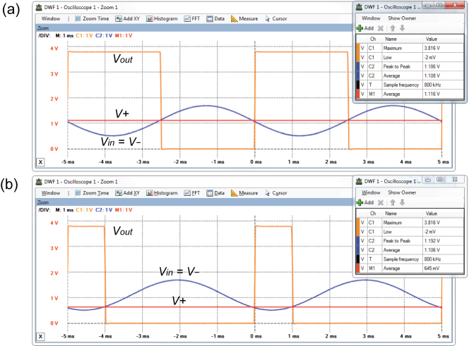
Figure 4-30: Output of the comparator circuit
If everything remains exactly the same but the potentiometer is adjusted to give a different value for V+, in this case 0.645 V, the output will be as shown in Figure 4-30(b), where the duty cycle of the output Vout will be different. This comparator circuit could also be used to detect low voltage conditions—for example, lighting a warning LED if a battery's voltage output fell below a certain value. The circuit example used in 4-29(b) could be used to generate a PWM signal with a controllable duty cycle, according to the controlling voltage V+.
The large open-loop gain means that op-amps are generally used with feedback, which is directed to the negative or positive op-amp input. This feedback opens up an enormous range of other applications for the op-amp.
Negative Feedback and Voltage Follower
Negative feedback is formed when you connect the output of an op-amp (Vout ) back to the inverting input (V−). When you apply a voltage (Vin ) to the noninverting input (V+) and increase it slowly, as Vin increases, then so would the difference between V+ and V−; however, the output voltage also increases according to G(V1 − V2), and this feeds back into the V− input, causing the output voltage Vout to be reduced. Essentially, the op-amp attempts to keep the voltage on the inverting (V−) input the same as the noninverting (V+) input by adjusting the output. The impact of this action is that the value of Vout is stabilized to be the same as the Vin voltage on V+; the higher the gain of the op-amp, the closer this difference will be to zero.
That action on its own is not very useful to us except that the current required to set the voltage on the input is small, and the op-amp can control much larger currents on the output side. Because the negative feedback keeps the output voltage the same as the input voltage, the configuration as a whole has a gain of 1. This configuration is known as a voltage follower, or unity-gain buffer, and is illustrated in Figure 4-31. This configuration is important, as it is used in Chapter 6 to protect the ADC circuitry in the Beagle boards, and it is also used to ensure that the ADC reference voltage is not modified by connecting it to a circuit.
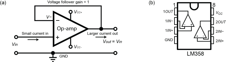
Figure 4-31: The voltage follower op-amp circuit
Positive Feedback
Negative feedback is the most common type of feedback used with op-amps because of its stabilizing impact. An op-amp in a positive feedback configuration is one in which the output is returned to the positive noninverting input of the op-amp. In such a case the feedback signal supports the input signal. For example, positive feedback can be used to add hysteresis to the open-loop op-amp comparator circuit, by connecting Vout to V+ through a positive feedback resistor. This can be used to reduce the comparator's response to noise on the input signal.
Concluding Advice
There is a lot of material covered in this chapter. So to finish, here is some general advice for working with electrical components and the Beagle boards:
- Never leave inputs floating. Use pull-up/pull-down resistors on all switches. Check whether unused IC pins need to be tied high/low.
- Ensure that all of the GNDs in your circuit are connected.
- Remember to power your chips with the correct voltage level.
- Don't assume that a new diode, FET, BJT, or logic gate has the same pin layout as the previous component that you used.
- Just like programming, build a simple circuit first, test it, and then add the next layer of complexity. Never assume something works!
- Don't leave wire joints and croc clip connections hanging where they could touch off each other—the same for resistors on breadboards.
- Use a flat-head screwdriver to remove ICs from breadboards, as it is very easy to bend the IC legs beyond repair.
- CMOS ICs are statically sensitive, so touching them with your fingers may damage them, due to the buildup of static electricity on your body. Touch the back of a computer or some grounding metal object before you touch the ICs.
- Don't assume that components have exact or consistent values—in particular, transistor gains and resistor ranges.
Summary
After completing this chapter, you should be able to do the following:
- Describe the basic principles of electrical circuit operation, build circuits on breadboards, and measure voltage and current values
- Use discrete components such as diodes, LEDs, transistors, and capacitors in your own circuit designs
- Use transistors and FETs as switches to control higher current and voltage signals than would be possible by using the Beagle board outputs on their own
- Interconnect and interface to logic gates, being particularly aware of the issues that arise with “floating” inputs
- Describe the principles of analog-to-digital conversion and design basic operational-amplifier circuits
- Combine all of these skills to build the type of circuits that are important for safely interfacing to the Beagle board GPIOs
Further Reading
Documents and links for further reading have been listed throughout this chapter, but here are some further reference documents:
- T. R. Kuphaldt, “Lessons in Electric Circuits,” a free series of textbooks on the subjects of electricity and electronics:
www.ibiblio.org/kuphaldt/electricCircuits/. - All About Circuits:
www.allaboutcircuits.comprovides excellent applied examples of many types of electronic circuits. - The Electronics Club:
www.electronicsclub.infoprovides electronics projects for beginners and for reference. - Neil Storey, Electronics: A Systems Approach, 5th ed., New York: Pearson, 2013.
Here is a full list of the components that are used in this chapter:
- Breadboard
- Diodes: 1N4001, general-purpose LED
- Transistors: NPN: BC547, FET: BS270
- Voltage regulator: KA7805/LM7805
- PTC: 60R110
- Button and Switch: General purpose SPST and SPDT
- ICs: 74HC73N, 74HC03N, 74LS08N, 74HC08N, 74HC14, LM358N
- Resistors: 1 MΩ, 2.2 kΩ, 2x10 kΩ, 50 kΩ, 100 Ω, 50 Ω, 1 kΩ, 470 Ω, 220 Ω, 100 kΩ POT
- Capacitors: 10 μF, 1 μF, 0.33 μF, 0.1 μF
- Optoisolator: SFH617A