
CHAPTER 8
Interfacing to the Beagle Board Buses
This chapter describes bus communication in detail, explaining and comparing the different bus types that are available on the Beagle boards. It describes how you can configure them for use, and how you can communicate with and control I2C, SPI, and UART devices, using both Linux tools and custom-developed C/C++ code. Practical examples are provided using different low-cost bus devices, such as a real-time clock, an accelerometer, a serial shift register with a seven-segment display, a USB-to-TTL 3.3V cable, and a GPS receiver. Finally, the AM335x DCAN controller is used to send and receive messages to and from a CAN Bus using Linux SocketCAN. After reading this chapter, you should have the skills necessary to begin interfacing almost any type of bus device to the Beagle boards.
EQUIPMENT REQUIRED FOR THIS CHAPTER:
- Any Beagle board
- A real-time clock on a breakout board (e.g., the DS3231)
- ADXL345 accelerometer on an I2C/SPI breakout board
- 74HC595 shift register, seven-segment display, and resistors
- A USB-to-TTL 3.3V cable (see Chapter 1 and Chapter 2)
- A low-cost UART GPS receiver (e.g., the GY-GPS6MV2)
- A low-cost physical-layer CAN Bus module (ideally one with a TI SN65HVD230 CAN controller)
Further details on this equipment and chapter are available at www.exploringbeaglebone.com/chapter8.
Introduction to Bus Communication
In Chapter 6, the use of general-purpose input/outputs (GPIOs) is discussed in detail, which makes it clear how you can connect a Beagle board to stand-alone components. This chapter examines more complex communications that can be performed using the bus interfaces that are available on the Beagle boards. Bus communication is a mechanism that enables data to be transferred between the high-level components of an embedded platform, using standardized communications protocols. The three most commonly used embedded system buses are available on the Beagle boards, and they are the subject of this chapter: Inter-Integrated Circuit (I2C), Serial Peripheral Interface (SPI), and Controller Area Network (CAN Bus). In addition, Universal Asynchronous Receiver/Transmitter (UART) devices are discussed. These are computer hardware devices that can be configured and used to send and receive serial data. When combined with appropriate driver interfaces, UARTs can implement standard serial communication protocols, such as RS-232, RS-422, or RS-485.
Understanding the behavior and use of bus communication protocols and devices enables the possibility of building advanced Beagle board electronic systems. There are a huge number of complex sensors, actuators, input devices, I/O expanders, and other microcontrollers that conform to these communication protocols, and the Beagle boards are capable of communicating with them all. Several such devices are used in Chapter 9 to interface the boards to the physical environment using sensors and actuators. In addition, Chapter 10 describes how you can use popular microcontrollers to build your own advanced bus devices, which can be interfaced directly to the boards using these buses.
The topics discussed in this chapter are all demonstrated using practical examples with devices that were largely chosen based on their wide availability and low cost. However, the focus of this chapter is on imparting an understanding of the techniques employed in using the board's buses, rather than just describing the specific bus devices used. To this end, the chapter provides generic communications code that you can use to apply the principles described to any device of your choosing.
I2C
Inter-Integrated Circuit (IIC or I2C) is a two-wire bus that was designed by Philips in the 1980s to interface microprocessors or microcontrollers to low-speed peripheral devices. A master device, such as a Beagle board, controls the bus, and many addressable slave devices can be attached to the same two wires. It has remained popular over the years, mainly because of its relative simplicity and breadth of adoption. It is currently used in smartphones, most microcontrollers, and even environmental management applications in large-scale server farms. Here are some general features of the I2C bus:
- Only two signal lines are required for communication, the Serial Data (SDA) line for the bidirectional transmission of data, and the Serial Clock (SCL) line, which is used to synchronize the data transfer. Because the bus uses this synchronizing clock signal, the data transfer is said to be synchronous. The transmission is said to be bidirectional because the same SDA wire can be used for sending and receiving data.
- Each device on the bus can act as a master or a slave. The master device is the one that initiates communication, and the slave device is the one that responds. Designated slave devices cannot initiate communication with the master device.
- Each slave device attached to the bus is pre-assigned a unique address, which is in either 7-bit or 10-bit form. In the following examples, 7-bit addressing is used, i.e.,
0x00to0x7F(27 = 12810 =0x80). - It has true multi-master bus facilities, including collision detection and arbitration if two or more master devices activate at once.
- On-chip noise filtering is built in as standard.
I2C Hardware
Figure 8-1 illustrates the interconnection of multiple slave devices to the I2C bus. All output connections to the SDA and SCL lines are in open-drain configuration (discussed in Chapter 4), whereby all devices share a common ground connection. This means that devices with different logic families can be intermixed on the bus and that a large number of devices can be added to a single bus. In theory, up to 128 devices could be attached to a single bus, but doing so would greatly increase the capacitance of the interconnecting lines. The bus is designed to work over short distances, as long bus lines are prone to electrical interference and capacitance effects (e.g., a pair of 22 AWG shielded wires has a capacitance of about 15pF/ft).
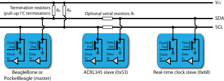
Figure 8-1: The I2C bus configuration
Transmission line capacitance has a huge impact on data transmission rates. In Chapter 4 (see Figure 4-11), when a 10μF capacitor is connected in parallel with a resistive load and an AC voltage supply is applied, the capacitor has a clear smoothing effect on the voltage across the load. This smoothing effect is unwelcome in the transmission of digital data; for example, if a random binary signal (0V–3.3V) switches at a high frequency, then severe smoothing could result in a constant 1.65V signal, which carries no binary information at all. Typically, the longer the bus length and the more I2C devices that are attached to it, the slower the speed of data transmission. There are I2C repeaters available that act as current amplifiers to help solve the problems associated with long lines. Further documentation on the I2C bus is available from NXP directly at tiny.cc/beagle801.
I2C on the Beagle Boards
I2C on the Beagle boards supports 7-bit/10-bit addressing, and bus frequencies of up to 400kHz. NXP (formerly Philips) has newer I2C Fast-mode Plus (Fm+) devices that can communicate at up to 1MHz1, but this capability is not available on the Beagle boards.
The I2C bus requires pull-up resistors (RP) on both the SDA and SCL lines, as illustrated in Figure 8-1. These are called termination resistors, and they usually have a value of between 1kΩ and 10kΩ. Their role is to pull the SDA and SCL lines up to VCC when no I2C device is pulling them down to GND. This pull-up configuration enables multiple master devices to take control of the bus and for the slave device to “stretch” the clock signal (i.e., hold SCL low). Clock stretching can be used by the slave device to slow down data transfer until it has finished processing and is ready to transmit. Termination resistors are often also present on the breakout board that is associated with an I2C device. This can be a useful feature, but their equivalent parallel resistance should be factored into your design, particularly if you are using several boards on the same bus. In the I2C demonstration application discussed in this chapter, the PocketBeagle is the master device, and the ADXL345 slave device is on a breakout board that already has 4.7kΩ termination resistors on the board.
The optional serial resistors (RS) shown in Figure 8-1 usually have low values (e.g., 250Ω) and can help protect against overcurrent conditions. The I2C devices are typically attached to the SDA and SCL lines using built-in Schmitt trigger inputs (see Chapter 4) to reduce the impact of signal noise by building in a degree of switching hysteresis.
I2C Devices on the Beagle Boards
The I2C buses are present by default on the Debian Linux image and are described in Table 8-1. The I2C devices are visible in the /dev/ directory.
Table 8-1: I2C Buses on the Debian Linux Image on the BeagleBone and PocketBeagle Boards
| H/W BUS | S/W DEVICE | SDA PIN | SCL PIN | DESCRIPTION |
| I2C0 |
/dev/i2c-0
|
N/A | N/A | Internal bus for HDMI control |
| I2C1 |
/dev/i2c-2
|
P9_18/P2.11 | P9_17/P2.9 | General I2C bus |
| I2C2 |
/dev/i2c-1
|
P9_20/P1.26 | P9_19/P1.28 | General I2C bus |
debian@ebb:/dev$ ls -l i2c*crw-rw---- 1 root i2c 89, 0 Jun 9 19:24 i2c-0crw-rw---- 1 root i2c 89, 1 Jun 9 19:25 i2c-1crw-rw---- 1 root i2c 89, 2 Jun 9 19:25 i2c-2
You can see that these devices are owned by the i2c group, and the user debian is a member of that group.
debian@ebb:/dev$ whoamidebiandebian@ebb:/dev$ groupsdebian … i2c … pwm gpio
The c file attribute indicates that these are character devices. A character device typically transfers data to and from a user application—they behave like pipes or serial ports, instantly reading or writing the byte data in a character-by-character stream. They provide the framework for many typical drivers, such as those that are required for interfacing to serial communications hardware.
An I2C Test Circuit
Many I2C devices are available that can be connected to the Beagle board, and two different types are described in this section—a real-time clock and an accelerometer. These particular devices have been chosen because they have a low cost, are widely available, are useful, and have high-quality datasheets.
A Real-Time Clock
Unlike a desktop computer, the Beagle boards do not have an onboard battery-backed clock. This means that the clock time is lost on each occasion that the board reboots; however, a network-attached Beagle board can retrieve the current time from the network using the Network Time Protocol (NTP). If you are using a board that cannot remain connected to a stable network, then a battery-backed real-time clock (RTC) can be a valuable addition.
Devices synchronize time with an RTC only occasionally, so RTCs are typically attached to an I2C bus. If you are purchasing a module, then you should ensure that it is supported by an LKM for your kernel (or by the kernel itself). This allows for full OS integration of the RTC, which is discussed shortly.
debian@ebb:~$ uname -aLinux ebb 4.14.44-ti-rt-r51 #1 SMP PREEMPT …debian@ebb:~$ cd /lib/modules/4.14.44-ti-rt-r51/debian@ebb:/lib/modules/4.14.44-ti-rt-r51$ cd kernel/drivers/rtc/debian@ebb:/lib/modules/4.14.44-ti-rt-r51/kernel/drivers/rtc$ lsrtc-bq4802.ko.xz rtc-ds1742.ko.xz rtc-msm6242.ko.xzrtc-cmos.ko.xz rtc-ds2404.ko.xz rtc-rp5c01.ko.xzrtc-ds1286.ko.xz rtc-hid-sensor-time.ko.xz …
And there is evidence of additional built-in drivers in:
debian@ebb:/sys/bus/i2c/drivers$ ls… at24 rtc-ds1307 rtc-max6900 rtc-rx8581 …
The DS3231 has been chosen for this chapter, as it is a high-accuracy RTC that keeps time to ±63 seconds per year (i.e., ±2ppm2 at 0°C–50°C), and it is widely available in module form at very low cost (even less than $1). The DS3231 is compatible with the DS1307 LKM (rtc-ds1307.ko) or built-in kernel code.
The ADXL345 Accelerometer
The Analog Devices ADXL345 is a small, low-cost accelerometer that can measure angular position with respect to the direction of the earth's gravitational force. For example, a single-axis accelerometer at rest on the surface of the earth, with the sensitive axis parallel to the earth's gravity, will measure an acceleration of 1g (9.81m/s2) straight upward. While accelerometers provide absolute orientation measurement, they suffer from high-frequency noise, so they are often paired with gyroscopes for accurate measurement of change in orientation (e.g., in game controllers)—a process known as sensor fusion. However, accelerometers have excellent characteristics for applications in which low-frequency absolute rotation is to be measured. For simplicity, an accelerometer is used on its own in the following discussions because the main aim is to impart an understanding of the I2C bus.
The ADXL345 can be set to measure values with a fixed 10-bit resolution or using a 13-bit resolution at up to ±16 g. The ADXL335 analog accelerometer is utilized in Chapter 9—it provides voltages on its outputs that are proportional to its orientation. Digital accelerometers such as the ADXL345 include analog-to-digital conversion circuitry along with real-time filtering capabilities—they are more complex devices with many configurable options, but it is actually easier to attach them to the board than their analog equivalents. The ADXL345 can be interfaced to the board using an I2C or SPI bus, which makes it an ideal sensor to use in this chapter as an example for both bus types. The chapter web page identifies suppliers from whom you can purchase this particular sensor.
The I2C slave address is determined by the slave device itself. For example, the ADXL345 breakout board has the address 0x53, which is determined at manufacture. Many devices, including the ADXL345, have selection inputs that allow you to alter this value within a defined range.3 If the device does not have address selection inputs, then you cannot connect two of them to the same bus, as their addresses will conflict. However, there are I2C multiplexers available that would enable you to overcome this problem.
The data sheet for the ADXL345 is an important document that should be read along with this chapter. It is available at www.analog.com/ADXL345.
Wiring the Test Circuit
Figure 8-2 illustrates a test circuit that can be used to evaluate the function of I2C devices that are attached to the PocketBeagle. In this circuit, an ADXL345 and a DS3231 breakout board are connected to the same I2C1 bus. The ADXL345 has the address 0x53, and the DS3231 has the address 0x68, so there will not be a conflict. The CS input of the ADXL345 breakout board is set high to place the module in I2C mode.
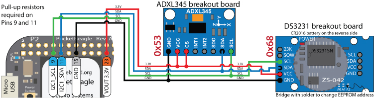
Figure 8-2: Two I2C devices connected to the I2C1 bus on the PocketBeagle board
Even if you do not have these particular sensors, the following discussion is fully representative of the steps required to connect any type of I2C sensor to the Beagle boards. See Table 8-1 for the pins to be used on the BeagleBone boards.
Using Linux I2C-Tools
Linux provides a set of tools, called i2c-tools, for interfacing to I2C bus devices; it includes a bus probing tool, a chip dumper, and register-level access helpers. You can install these tools using the following command:
debian@ebb:~$ sudo apt install i2c-tools i2cdetect
The first step is to detect that the devices are present on the bus. When the I2C buses are enabled, the i2cdetect command displays this:
debian@ebb:~$ i2cdetect -li2c-1 i2c OMAP I2C adapter I2C adapteri2c-2 i2c OMAP I2C adapter I2C adapteri2c-0 i2c OMAP I2C adapter I2C adapter
If the circuit is wired as in Figure 8-2 with an ADXL345 and a DS3231 breakout board attached to the /dev/i2c-1 bus, then it can be probed for connected devices, which will result in the following output:
debian@ebb:~$ i2cdetect -y -r 10 1 2 3 4 5 6 7 8 9 a b c d e f00: -- -- -- -- -- -- -- -- -- -- -- -- --10: -- -- -- -- -- -- -- -- -- -- -- -- -- -- -- --20: -- -- -- -- -- -- -- -- -- -- -- -- -- -- -- --30: -- -- -- -- -- -- -- -- -- -- -- -- -- -- -- --40: -- -- -- -- -- -- -- -- -- -- -- -- -- -- -- --50: -- -- -- 53 -- -- 56 -- -- -- -- -- -- -- -- --60: -- -- -- -- -- -- -- -- 68 -- -- -- -- -- -- --70: -- -- -- -- -- -- -- --
Hexadecimal addresses in the range 0x03 to 0x77 are displayed by default. Using -a will display the full range 0x00 to 0x7F. When -- is displayed, the address was probed, but no device responded. If UU is displayed, then probing was skipped, as the address is already in use by a driver.
The ADXL345 breakout board occupies address 0x53, and the DS3231 ZS-042 breakout board occupies addresses 0x68 and 0x56.4 Each of the attached breakout boards defines its own addresses, which means that problems will arise if two slave devices with the same address are connected to a single bus. Many I2C devices provide an address selection option that often involves setting an additional input high/low, which is typically implemented on breakout boards by jumper connections or contact points that can be bridged with solder.
i2cdump
The i2cdump command can be used to read in the values of the registers of the device attached to an I2C bus and display them in a hexadecimal block form. You should not use this command without consulting the datasheet for the slave device, as in certain modes the i2cdump command will write to the device. The argument -y ignores a related warning. The devices in Figure 8-2 can be safely used, and when the address 0x68 is probed on the i2c-1 bus in byte mode (b), it results in the following output:
debian@ebb:~$ i2cdump -y 1 0x68 b0 1 2 3 4 5 6 7 8 9 a b c d e f 0123456789abcdef00: 19 02 03 06 25 10 02 00 00 00 00 00 00 00 1c 88 ????%??…….??10: 00 17 00 XX XX XX XX XX XX XX XX XX XX XX XX XX .?.XXXXXXXXXXXXX
If the device is probed again in quick succession, then a similar output results, but in this example the register value for address 0x00 changes from 19 to 41. This value actually represents the number of clock seconds (in decimal form) on the RTC module. Therefore, 22 seconds had elapsed between these two calls to the i2cdump command.
debian@ebb:~$ i2cdump -y 1 0x68 b0 1 2 3 4 5 6 7 8 9 a b c d e f 0123456789abcdef00: 41 02 03 06 25 10 02 00 00 00 00 00 00 00 1c 88 A???%??…….??10: 00 17 00 XX XX XX XX XX XX XX XX XX XX XX XX XX .?.XXXXXXXXXXXXX
To understand the meaning of such registers, you need to read the datasheet for the device. The datasheet for the DS3231 is available at tiny.cc/beagle802, and the most important registers are illustrated in Figure 8-3. In this figure, the hwclock function (see the feature on Utilizing Linux Hardware RTC Devices that follows) is used to display the time value from the RTC module. The i2cdump command is called (a few seconds later) to display the registers, allowing their meaning to be verified. Note that the Irish standard time (IST) time zone results in a shift of plus one hour from UTC/GMT.
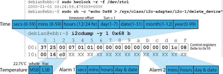
Figure 8-3: The DS3231 registers summary
i2cget
The i2cget command can be used to read the value of a register to test the device or as an input for Linux shell scripts. For example, to read the number of seconds on the clock, you can use the following:
debian@ebb:~$ i2cget -y 1 0x68 0x000x30
The Analog Discovery digital logic analyzer functionality can be used to analyze the physical I2C bus to view the interaction of the SDA and SCL signals as data is written to and read from the I2C bus. The logic analyzer functionality has interpreters for I2C buses, SPI buses, CAN buses, and UART communication, which can display the numerical equivalent values of the serial data carried on the bus. Figure 8-4 captures the signal transitions of the i2cget command used in the preceding example. Here, you can see that the clock is running at I2C standard data transfer mode (i.e., 100kHz).

Figure 8-4: Using i2cget to read the number of seconds on the RTC from register 0x00
The ADXL345 accelerometer can be accessed in the same way as the RTC module. Figure 8-5 illustrates the important registers that are utilized in this chapter. To test that the ADXL345 is correctly connected to the bus, read the DEVID of the attached device, which should be returned as 0xE5.
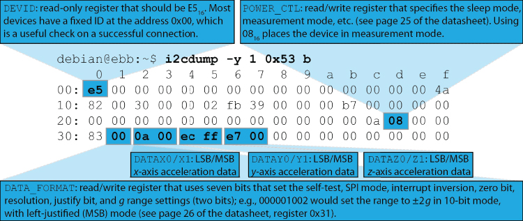
Figure 8-5: Important ADXL345 registers
debian@ebb:~$ i2cget -y 1 0x53 0x000xe5
You can see that the first value at address 0x00 is 0xE5, and this value corresponds to the DEVID entry in Figure 8-5—successful communication has been verified.
i2cset
As previously stated, the datasheet for the ADXL345 from Analog Devices is available at www.analog.com/ADXL345. It is a comprehensive and well-written datasheet that details every feature of the device. In fact, the real challenge in working with new bus devices is in decoding the datasheet and the intricacies of the device's behavior. The ADXL345 has 30 public registers, and Figure 8-5 illustrates those that are accessed in this chapter. Other registers enable you to set power save inactivity periods, orientation offsets, and interrupt settings for free-fall, tap, and double-tap detection.
The x-, y-, and z-axis acceleration values are stored using a 10-bit or 13-bit resolution; therefore, two bytes are required for each reading. Also, the data is in 16-bit two's complement form (see Chapter 4). To sample at 13 bits, the ADXL345 must be set to the ±16 g range. Figure 8-6 (based on the ADXL345 datasheet) describes the signal sequences required to read and write to the device. For example, to write a single byte to a device register, the master/slave access pattern in the first row is used as follows:
- The master sends a start bit (i.e., it pulls SDA low, while SCL is high).
- While the clock toggles, the 7-bit slave address is transmitted one bit at a time.
- A read bit (1) or write bit (0) is sent, depending on whether the master wants to read or write to/from a slave register.
- The slave responds with an acknowledge bit (ACK = 0).
- In write mode, the master sends a byte of data one bit at a time, after which the slave sends back an ACK bit. To write to a register, the register address is sent, followed by the data value to be written.
- Finally, to conclude communication, the master sends a stop bit (i.e., it allows SDA to float high, while SCL is high).
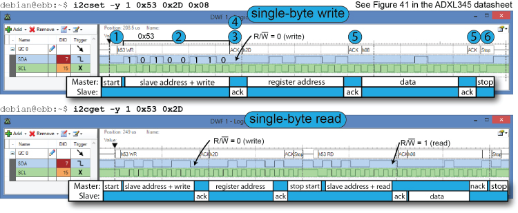
Figure 8-6: Capture and timings required for communication with the ADXL345 device
The i2cset command can be used to set a register. This is required, for example, to take the ADXL345 out of power-saving mode, by writing 0x08 to the POWER_CTL register, which is at 0x2D. The value is written and then confirmed as follows:
debian@ebb:~$ i2cset -y 1 0x53 0x2D 0x08debian@ebb:~$ i2cget -y 1 0x53 0x2D0x08
The call to i2cset and i2cget invokes the handshaking sequences that are described in the ADXL345 datasheet and illustrated in Figure 8-6, which also identifies these numbered steps.
When the i2cdump command is subsequently used, the registers 0x32 through 0x37 (as identified in Figure 8-5) display the acceleration values, which change as the sensor is physically rotated and the i2cdump command is repeatedly called. The next step is to write program code that can interpret the values contained in the DS3231 and the ADXL345 registers.
I2C Communication in C
The first C program example, in Listing 8-1, reads in all of the DS3231 RTC registers and displays the current time and temperature. The time is contained in binary coded decimal (BCD) form in registers 0x00 (seconds), 0x01 (minutes), and 0x02 (hours). The temperature is in hexadecimal form in registers 0x11 (whole number temperature) and in the two most-significant bits of 0x12 (the fractional part—i.e., 002=0, 012=¼, 102=½, and 112=¾).
This is a useful first example because it is self-contained, will work on all generic embedded Linux platforms, and can be adapted for other I2C devices.
Listing 8-1: exploringbb/chp08/i2c/test/testDS3231.c
#include<stdio.h>#include<fcntl.h>#include<sys/ioctl.h>#include<linux/i2c.h>#include<linux/i2c-dev.h>#include<unistd.h>#define BUFFER_SIZE 19 //0x00 to 0x13// the time is in the registers in encoded decimal formint bcdToDec(char b) { return (b/16)*10 + (b%16); }int main(){int file;printf("Starting the DS3231 test application ");if((file=open("/dev/i2c-1", O_RDWR)) < 0){perror("failed to open the bus ");return 1;}if(ioctl(file, I2C_SLAVE, 0x68) < 0){perror("Failed to connect to the sensor ");return 1;}char writeBuffer[1] = {0x00};if(write(file, writeBuffer, 1)!=1){perror("Failed to reset the read address ");return 1;}char buf[BUFFER_SIZE];if(read(file, buf, BUFFER_SIZE)!=BUFFER_SIZE){perror("Failed to read in the buffer ");return 1;}printf("The RTC time is %02d:%02d:%02d ", bcdToDec(buf[2]),bcdToDec(buf[1]), bcdToDec(buf[0]));// note that 0x11 = 17 decimal and 0x12 = 18 decimalfloat temperature = buf[0x11] + ((buf[0x12]>>6)*0.25);printf("The temperature is %f°C ", temperature);close(file);return 0;}
The code can be built and executed as follows:
debian@ebb:~/exploringbb/chp08/i2c/test$ gcc testDS3231.c -o testDS3231debian@ebb:~/exploringbb/chp08/i2c/test$ ./testDS3231Starting the DS3231 test applicationThe RTC time is 00:53:46The temperature is 22.50°C
The temperature functionality is used to improve this RTC's accuracy by modeling the impact of environmental temperature on time keeping—it is updated every 64 seconds, and it is accurate only to ±3°C.
The ADXL345 digital accelerometer measures acceleration in three axes using analog sensors, which are internally sampled and filtered according to the settings that are placed in its registers. The acceleration values are then available for you to read from these registers. Therefore, the sensor performs timing-critical signal processing that would otherwise need to be performed by the Beagle board. However, further numerical processing is still required in converting the 16-bit two's complement values stored in its registers into values that describe angular pitch and roll. As such, C/C++ is a good choice for this type of numerical processing if real-time performance is required.
To display all the registers and to process the accelerometer values, a new program (chp08/i2c/test/ADXL345.cpp) is written that breaks the calls into functions, such as the readRegisters() function.
int readRegisters(int file){ // read all 64(0x40) registers to a bufferwriteRegister(file, 0x00, 0x00); // set address to 0x00 for block readif(read(file, dataBuffer, BUFFER_SIZE)!=BUFFER_SIZE){cout << "Failed to read in the full buffer." << endl;return 1;}if(dataBuffer[DEVID]!=0xE5){cout << "Problem detected! Device ID is wrong" << endl;return 1;}return 0;}
This code writes the address 0x00 to the device, causing it to send back the full 64 (0x40) registers (BUFFER_SIZE). To process the two raw 8-bit acceleration registers, code to combine two bytes into a single 16-bit value is written as follows:
short combineValues(unsigned char upper, unsigned char lower){//shift the MSB left by 8 bits and OR with the LSBreturn ((short)upper<<8)|(short)lower;}
The types of the data are vital in this function, as the register data is returned in two's complement form. If an int type (of size 32 bits, int32_t) were used instead of short 16-bit integral data (int16_t), then the sign bit would be located in the incorrect bit position (i.e., not at the MSB, bit 31). This function shifts the upper byte left (multiply) by eight places (equivalent to a multiplication by 28 = 256) and ORs the result with the lower byte, which replaces the lower byte with eight zeros that are introduced by the shift. This results in a 16-bit signed value (int16_t) that has been created from two separate 8-bit values (uint8_t). When executed, the ADXL345.cpp application will give the following output, with the program updating the acceleration data on the same terminal shell line:
debian@ebb:~/exploringbb/chp08/i2c/test$ g++ ADXL345.cpp -o ADXL345debian@ebb:~/exploringbb/chp08/i2c/test$ ./ADXL345Starting the ADXL345 sensor applicationThe Device ID is: e5The POWER_CTL mode is: 08The DATA_FORMAT is: 00X=40 Y=1 Z=276 sample=12
Additional code is required to convert these values into pitch and roll form. This is added to the C++ class in the next section. For your information, the logic analyzer indicates that it takes 4.19ms to read in the full set of 64 registers at a bus speed of 100kHz.
Wrapping I2C Devices with C++ Classes
Object-oriented programming is described in Chapter 5 as a suitable framework for developing code for embedded systems. A specific C++ class can be written to wrap the functionality of the ADXL345 accelerometer; because it is likely that you will need to write code to control several different types of I2C devices, it would be useful if the general I2C code could be extracted and placed in a parent class. To this end, a class has been written for this chapter called I2CDevice that captures the general functionality you would associate with an I2C bus device. You can extend this code to control any type of I2C device. It can be found in the I2CDevice.cpp and I2CDevice.h files in the chp08/i2c/cpp/ directory. The class has the structure described in Listing 8-2.
Listing 8-2: /exploringbb/chp08/i2c/cpp/I2CDevice.h
class I2CDevice {private:unsigned int bus, device;int file;public:I2CDevice(unsigned int bus, unsigned int device);virtual int open();virtual int write(unsigned char value);virtual unsigned char readRegister(unsigned int registerAddress);virtual unsigned char* readRegisters(unsigned int number,unsigned int fromAddress=0);virtual int writeRegister(unsigned int registerAddress, unsignedchar value);virtual void debugDumpRegisters(unsigned int number);virtual void close();virtual ~I2CDevice();};
The implementation code is available in the chp08/i2c/cpp/ directory. This class can be extended to control any type of I2C device, and in this case it is used as the parent of a specific device implementation class called ADXL345. Therefore, you can say that ADXL345 is an I2CDevice. This inheritance relationship means that any methods available in the I2CDevice class are now available in the ADXL345 class in Listing 8-3 (e.g., readRegister()).
Listing 8-3: /exploringbb/chp08/i2c/cpp/ADXL345.h
class ADXL345:protected I2CDevice{// protected inheritance means that the public I2C methods are no// longer publicly accessible by an object of the ADXL345 classpublic:enum RANGE { // enumerations are used to limit the optionsPLUSMINUS_2_G = 0,PLUSMINUS_4_G = 1,PLUSMINUS_8_G = 2,PLUSMINUS_16_G = 3};enum RESOLUTION { NORMAL = 0, HIGH = 1 };private:unsigned int I2CBus, I2CAddress;unsigned char *registers;ADXL345::RANGE range;ADXL345::RESOLUTION resolution;short accelerationX, accelerationY, accelerationZ;float pitch, roll; // in degreesshort combineRegisters(unsigned char msb, unsigned char lsb);void calculatePitchAndRoll();virtual int updateRegisters();public:ADXL345(unsigned int I2CBus, unsigned int I2CAddress=0x53);virtual int readSensorState();virtual void setRange(ADXL345::RANGE range);virtual ADXL345::RANGE getRange() { return this->range; }virtual void setResolution(ADXL345::RESOLUTION resolution);virtual ADXL345::RESOLUTION getResolution() {return this->resolution;}virtual short getAccelerationX() { return accelerationX; }virtual short getAccelerationY() { return accelerationY; }virtual short getAccelerationZ() { return accelerationZ; }virtual float getPitch() { return pitch; }virtual float getRoll() { return roll; }virtual void displayPitchAndRoll(int iterations = 600);virtual ~ADXL345();};
The enumerations are used to constrain the range and resolution selections to contain only valid options. A short example (application.cpp) can be used to test this structure, as follows:
int main(){ADXL345 sensor(1,0x53); // sensor is on bus 1 at the address 0x53sensor.setResolution(ADXL345::NORMAL); //using 10-bit resolutionsensor.setRange(ADXL345::PLUSMINUS_4_G); //range is +/-4gsensor.displayPitchAndRoll(); // put the sensor in display modereturn 0;}
This code can be built and executed as follows, where the pitch and roll are angular values that each vary between ±90°:
/chp08/i2c/cpp $ g++ application.cpp I2CDevice.cpp ADXL345.cpp -o ADXL345debian@ebb:~/exploringbb/chp08/i2c/cpp$ ./ADXL345Pitch:42.0089 Roll:-4.03966
You can use this approach to build wrapper classes for any type of I2C sensor on any type of embedded Linux device.
SPI
The Serial Peripheral Interface (SPI) bus is a fast, full-duplex synchronous serial data link that enables devices such as the Beagle board to communicate with other devices over short distances. Therefore, like I2C, the SPI bus is synchronous, but unlike the I2C bus, the SPI bus is full duplex. This means that it can transmit and receive data at the same time, by using separate lines for both sending data and receiving data.
In this section, the SPI bus is introduced, and two separate applications are developed. The first uses the SPI bus to drive a seven-segment LED display using the ubiquitous 74HC595 8-bit shift register. The second application interfaces to the ADXL345 accelerometer again, this time using its SPI bus instead of the I2C bus used previously.
SPI Hardware
SPI communication takes place between a single master device and one or more slave devices. Figure 8-7(a) illustrates a single slave example, where four signal lines are connected between the PocketBeagle master and slave devices. To communicate with the slave device, the following steps take place:
- The SPI master defines the clock frequency at which to synchronize the data communication channels.
- The SPI master pulls the chip select (CS) line low, which activates the client device—it is therefore said to be active low. This line is also known as slave select (SS).
- After a short delay, the SPI master issues clock cycles, sending data out on the master out - slave in (MOSI) line and receiving data on the master in - slave out (MISO) line. The SPI slave device reads data from the MOSI line and transmits data on the MISO line. One bit is sent and one bit is received on each clock cycle. The data is usually sent in 1-byte (8-bit) chunks.
- When complete, the SPI master stops sending a clock signal and then pulls the CS line high, deactivating the SPI slave device.

Figure 8-7: (a) Using SPI to connect to one slave device from the PocketBeagle, and (b) testing SPI using a loopback configuration on the BeagleBone
Unlike I2C, the SPI bus does not require pull-up resistors on the communication lines, so connections are straightforward. A summary comparison of I2C versus SPI is provided in Table 8-2.
Table 8-2: Comparison of I2C vs. SPI on the Beagle Board
| I2C | SPI | |
| Connectivity | Two wires, to which up to 128 addressable devices can be attached. | Typically four wires and requires additional logic for more than one slave device. |
| Data rate | I2C fast mode is 400 kHz. It uses half-duplex communication. | Faster performance (~10MHz) on the Beagle boards. It uses full duplex (except the three-wire variant). |
| Hardware | Pull-up resistors required. | No pull-up resistors required. |
| Support | Fully supported with two external buses (plus one HDMI). | Fully supported with one bus. There are two slave selection pins on all boards. |
| Features | Can have multiple masters. Slaves have addresses, acknowledge transfer, and can control the flow of data. | Simple and fast, but only one master device, no addressing, and no slave control of data flow. |
| Application | Intermittently accessed devices, e.g., RTCs, EEPROMs. | For devices that provide data streams, e.g., ADCs. |
The SPI bus operates using one of four different modes, which are chosen according to the specification defined in the SPI device's datasheet. Data is synchronized using the clock signal, and one of the SPI communication modes listed in Table 8-3 is set to describe how the synchronization is performed. The clock polarity defines whether the clock is low or high when it is idle (i.e., when CS is high). The clock phase defines whether the data on the MOSI and MISO lines is captured on the rising edge or falling edge of the clock signal. When a clock's polarity is 1, the clock signal is equivalent to an inverted version of the same signal with a polarity of 0. Therefore, a rising edge on one form of clock signal polarity is the equivalent of a falling edge on the other. You need to examine the datasheet for the slave device to determine the correct SPI mode to use.
Table 8-3: SPI Communication Modes
| MODE | CLOCK POLARITY (CPOL) | CLOCK PHASE (CPHA) |
| 0 | 0 (low at idle) | 0 (data captured on the rising edge of the clock signal) |
| 1 | 0 (low at idle) | 1 (data captured on the falling edge of the clock signal) |
| 2 | 1 (high at idle) | 0 (data captured on the falling edge of the clock signal) |
| 3 | 1 (high at idle) | 1 (data captured on the rising edge of the clock signal) |
The SPI protocol itself does not define a maximum data rate, flow control, or communication acknowledgment. Therefore, implementations vary from device to device, so it is important to study the datasheet of each type of SPI slave device. There are some three-wire SPI variants that use a single bidirectional MISO/MOSI line instead of two individual lines. For example, the ADXL345 sensor supports I2C, and both four-wire and three-wire SPI communication.
SPI on the Beagle Boards
The tables illustrated in Figure 6-6 and Figure 6-7 of Chapter 6 identify that the SPI buses are accessible from the GPIO headers as summarized in Table 8-4. Please note that SPI0 is not available by default on the BeagleBone and therefore must be enabled.
Table 8-4: Example SPI Pins on the Beagle Boards
| BBB SPI0 | BBB SPI1 | POCKET SPI0 | POCKET SPI1 | |
| Chip Select | P9_17 | P9_28 | P1.06 | P2.31 |
| MOSI | P9_18 | P9_29 | P1.12 | P2.25 |
| MISO | P9_21 | P9_30 | P1.10 | P2.27 |
| Clock | P9_22 | P9_31 | P1.08 | P2.29 |
The Linux devices are available in the /dev/ directory.
debian@ebb:/dev$ ls -l spi*crw-rw---- 1 root spi 153, 0 Jan 1 2000 spidev0.0crw-rw---- 1 root spi 153, 1 Jan 1 2000 spidev1.0crw-rw---- 1 root spi 153, 2 Jan 1 2000 spidev1.1
Despite that there are two entries in /dev/ for spidev1, there exists only one SPI device for spidev1, which has two different enable modes (0 and 1).
Testing an SPI Bus
To test the SPI bus, you can use a program called spidev_test.c that is available from www.kernel.org. However, the latest version at the time of writing has added support for dual and quad data-wire SPI transfers, which are not supported on the Beagle boards. An older version of this code has been placed in /chp08/spi/spidev_test/ and can be built using the following:
…/chp08/spi/spidev_test$ gcc spidev_test.c -o spidev_test If this code is executed without connecting to the SPI1 pins, then the output displayed by the spidev_test program will consist of a block of 0x00 or 0xFF values, depending on whether the MISO pin is configured in pull-down or pull-up configuration, respectively.
…/chp08/spi/spidev_test$ ./spidev_test -D /dev/spidev1.0spi mode: 0bits per word: 8max speed: 500000 Hz (500 KHz)FF FF FF FF FF FFFF FF FF FF FF FFFF FF FF FF FF FFFF FF FF FF FF FFFF FF FF FF FF FFFF FF FF FF FF FFFF FF
The source code for the spidev_test.c program includes a hard-coded array of values to test that the SPI communications line is working correctly. These values are as follows:
uint8_t tx[] = {0xFF, 0xFF, 0xFF, 0xFF, 0xFF, 0xFF,0x40, 0x00, 0x00, 0x00, 0x00, 0x95,0xFF, 0xFF, 0xFF, 0xFF, 0xFF, 0xFF,0xFF, 0xFF, 0xFF, 0xFF, 0xFF, 0xFF,0xFF, 0xFF, 0xFF, 0xFF, 0xFF, 0xFF,0xDE, 0xAD, 0xBE, 0xEF, 0xBA, 0xAD,0xF0, 0x0D,};
if the SPI MOSI and SPI MISO pins are connected together, as illustrated in Figure 8-7(b) for SPI0. To test SPI0 on the BeagleBone, use P9_29 and P9_30, and on the PocketBeagle, use P2.25 and P2.27. When the test program is executed again, the output should be as follows:
…/chp08/spi/spidev_test$ ./spidev_test -D /dev/spidev1.0spi mode: 0bits per word: 8max speed: 500000 Hz (500 KHz)FF FF FF FF FF FF40 00 00 00 00 95FF FF FF FF FF FFFF FF FF FF FF FFFF FF FF FF FF FFDE AD BE EF BA ADF0 0D
This is the exact block of data that is defined in the tx[] array inside the spidev_test.c code. Therefore, in this case, the block of data has been successfully transmitted from SPI1 MOSI and received by SPI1 MISO. You can see the same stream of data captured using the logic analyzer in Figure 8-8. The clock frequency of SCLK is 500kHz.
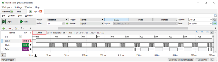
Figure 8-8: The SPI hardware loopback test on the PocketBeagle at 500kHz
This program can be executed on the SPI0 bus as follows:
…/chp08/spi/spidev_test$ ./spidev_test -D /dev/spidev0.0 A First SPI Application (74HC595)
The first circuit application to test the SPI bus is illustrated in Figure 8-9. It uses a 74HC595, which is an 8-bit shift register with latched outputs that can be supplied at 3.3V logic levels. The 74HC595 can typically be used at frequencies of 20MHz or greater, depending on the supply voltage VCC. The circuit in Figure 8-9 uses a seven-segment display and resistors to create a circuit that can display seven-segment symbols.
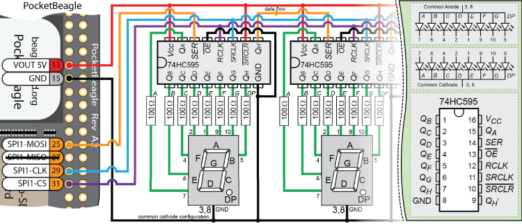
Figure 8-9: The 74HC595 seven-segment display SPI example (supports multiple display modules)
Seven-segment displays typically consist of eight LEDs that can be used to display decimal or hexadecimal numerals with a “decimal” point. They are available in a range of sizes and colors and are described as being either common cathode or common anode displays. This means the cathodes or anodes of the array of LEDs that make up the display are connected together as on the top right of Figure 8-9. You should not limit the current passing through the display by placing a single resistor on the common anode or the common cathode connection, as the limited current will be shared among the segments that are lighting. This results in an uneven light level, the intensity of which depends on the number of segments that are lit. Therefore, eight current-limiting resistors (or a resistor network) are required for each seven-segment display.
It is possible to drive these displays using eight GPIO pins per seven-segment module, but using serial shift registers and the SPI interface has the advantage of requiring only three SPI pins, regardless of the number of segments that are daisy chained together.
Wiring the 74HC595 Circuit
The 74HC595 is connected to the PocketBeagle using three of the four SPI lines, as a MISO response from the 74HC595 is not required. In addition to the 5V and GND inputs, the SPI connections are as follows:
- SPI1-CLK is connected to the Serial Clock input (pin 11) of the 74HC595. This line is used to synchronize the transfer of SPI data on the MOSI line.
- SPI1-MOSI is the MOSI line and is used to transfer the data from the PocketBeagle to the 74HC595 Serial Input (pin 14). This will send one byte at a time, which is the full capacity of the 74HC595.
- SPI-CS is connected to the Serial Register Clock input, which is used to latch the 74HC595 state to the output pins, thus lighting the LEDs.
To avoid the need for an external power supply, this circuit is powered using the board's 5V supply. However, this means that the circuit is now using 5V logic levels, and it would damage your board if you were to connect any of the 74HC595 outputs (e.g., QH’) back to the board.
You can safely connect the board's MOSI line directly to the circuit, as a 3.3V output can be safely connected to a 5V input. However, strictly speaking, 3.3V is slightly below the threshold of 3.5V (i.e., 30 percent below 5V) required for an input to a 5V logic-level CMOS IC (see Figure 4-24 in Chapter 4). In practice, the circuit works fine; however, a 74LS595 (at VCC = 5V) or a 74LVC595 (at VCC = 3.3V) would be more appropriate, despite their high cost and lack of availability.
The LEDs on the seven-segment display will light according to the byte that is transferred. For example, sending 0xAA should light every second LED segment (including the dot) if the setup is working correctly, as 0xAA = 101010102. This circuit is useful for controlling eight outputs using a single serial data line, and it can be extended to further seven-segment displays by daisy chaining 74HC595 ICs together, as indicated in Figure 8-9.
Once the SPI device is enabled on the Beagle board, you can write directly to the device as follows to light most of the LEDs (-n suppresses the newline character, -e enables escape character interpretation, and x escapes the subsequent value as hexadecimal):
debian@ebb:~$ echo -ne "xFF" > /dev/spidev1.1 The following will turn most of the LEDs off.
debian@ebb:~$ echo -ne "x00" > /dev/spidev1.1 This may not work exactly as expected, as the current SPI communication mode does not align by default with the operation of the 74HC595, as wired in Figure 8-9. However, it is a useful test to confirm that there is some level of response from the circuit. The transfer mode issue is resolved within the code example in the next section.
SPI Communication Using C
A C program can be written to control the seven-segment display. Basic open() and close() operations on the /dev/spidevX.Y devices work, but if you need to alter the low-level SPI transfer parameters, then a more sophisticated interface is required.
The following program uses the Linux user space SPI API, which supports reading and writing to SPI slave devices. It is accessed using Linux ioctl() requests, which support SPI through the sys/ioctl.h and linux/spi/spidev.h header files. A full guide on the use of this API is available at www.kernel.org/doc/Documentation/spi/.
The program in Listing 8-4 counts in hexadecimal (i.e., 0 to F) on a single seven-segment display using the encoded value for each digit. For example, 0 is obtained by lighting only the segments A, B, C, D, E, and F in Figure 8-10—this value is encoded as 0b00111111 in Listing 8-4, where A is the LSB (on the right) and H (the dot) is the MSB (on the left) of the encoded value. The transfer() function is the most important part of the code example, as it transfers each encoded value to the 74HC595 IC.

Figure 8-10: The 74HC595 SPI signal and output
Listing 8-4: /exploringbb/chp08/spi/spi595Example/spi595.c
#include<stdio.h>#include<fcntl.h>#include<unistd.h>#include<sys/ioctl.h>#include<stdint.h>#include<linux/spi/spidev.h>#define SPI_PATH "/dev/spidev1.1"// The binary data that describes the LED state for each symbol// A(top) B(top right) C(bottom right) D(bottom)// E(bottom left) F(top left) G(middle) H(dot)const unsigned char symbols[16] = { //(msb) HGFEDCBA (lsb)0b00111111, 0b00000110, 0b01011011, 0b01001111, // 01230b01100110, 0b01101101, 0b01111101, 0b00000111, // 45670b01111111, 0b01100111, 0b01110111, 0b01111100, // 89Ab0b00111001, 0b01011110, 0b01111001, 0b01110001 // CdEF};int transfer(int fd, unsigned char send[], unsigned char rec[], int len){struct spi_ioc_transfer transfer; //transfer structuretransfer.tx_buf = (unsigned long) send; //buffer for sending datatransfer.rx_buf = (unsigned long) rec; //buffer for receiving datatransfer.len = len; //length of buffertransfer.speed_hz = 1000000; //speed in Hztransfer.bits_per_word = 8; //bits per wordtransfer.delay_usecs = 0; //delay in ustransfer.cs_change = 0; // affects chip select after transfertransfer.tx_nbits = 0; // no. bits for writing (default 0)transfer.rx_nbits = 0; // no. bits for reading (default 0)transfer.pad = 0; // interbyte delay - check version// send the SPI message (all of the above fields, inc. buffers)int status = ioctl(fd, SPI_IOC_MESSAGE(1), &transfer);if (status < 0) {perror("SPI: SPI_IOC_MESSAGE Failed");return -1;}return status;}int main(){int fd, i; // file handle and loop counterunsigned char null=0x00; // sending only a single charuint8_t mode = 3; // SPI mode 3// The following calls set up the SPI bus propertiesif ((fd = open(SPI_PATH, O_RDWR))<0){perror("SPI Error: Can't open device.");return -1;}if (ioctl(fd, SPI_IOC_WR_MODE, &mode)==-1){perror("SPI: Can't set SPI mode.");return -1;}if (ioctl(fd, SPI_IOC_RD_MODE, &mode)==-1){perror("SPI: Can't get SPI mode.");return -1;}printf("SPI Mode is: %d ", mode);printf("Counting in hexadecimal from 0 to F now: ");for (i=0; i<=15; i++){// This function can send and receive data, just sending nowif (transfer(fd, (unsigned char*) &symbols[i], &null, 1)==-1){perror("Failed to update the display");return -1;}printf("%4d ", i); // print the number in the terminal windowfflush(stdout); // need to flush the output, nousleep(500000); // sleep for 500ms each loop}close(fd); // close the filereturn 0;}
The main() function sets the SPI control parameters. These are ioctl() requests that allow you to override the device's current settings for parameters such as the following, where xx is both RD (read) and RW (write):
SPI_IOC_xx_MODE: The SPI transfer mode (0–3).SPI_IOC_xx_BITS_PER_WORD: The number of bits in each word.SPI_IOC_xx_LSB_FIRST: 0 is MSB first, 1 is LSB first.SPI_IOC_xx_MAX_SPEED_HZ: The maximum transfer rate in Hz.
The current Linux implementation provides for synchronous transfers only. When executed, this code results in the following output, where the count value continually increases (0 to F) on the one line of the terminal window:
debian@ebb:~/exploringbb/chp08/spi/spi595Example$ ./spi595SPI Mode is: 3Counting in hexadecimal from 0 to F now:5
At the same time, this code is sending signals to the 74HC595 as captured using the SPI interpreter of the logic analyzer in Figure 8-10, in which the symbol 0 is being displayed by the seven-segment display (i.e., 0b00111111). During this time period, the CS (SPI1-CS) line is pulled low, while the SCLK clock (SPI1-CLK) that is “high at idle” is toggled by the SPI master after a short delay. The data is then sent on the SDIO (SPI1-MOSI) line, MSB first, to the 74HC595, and it is transferred on the rising edge of the clock signal. This confirms that the SPI transfer is taking place in mode 3, as described in Table 8-3.
The data transfer takes ~9μs. This means that if the channel were held open, it would be capable of transferring a maximum of ~111kB/s (~0.9Mb/s) at a processor clock rate of 1MHz.
Bidirectional SPI Communication in C/C++
The 74HC595 example only sends data from the board to the 74HC595 and as such is a unidirectional communication example. In this section, a bidirectional communication example is developed that involves using the registers on the ADXL345 sensor. As discussed previously, the ADXL345 has both an I2C and an SPI communications interface. This makes it a useful device with which to examine bidirectional SPI communication, as the register structure is already described in detail earlier in this chapter.
The ADXL345 SPI Interface
SPI is not a formal standard with a standards body controlling its implementation, and therefore it is vital that you study the datasheet for the device that you want to attach to your Beagle board. In particular, the SPI communication timing diagram should be studied in detail. This is presented for the ADXL345 in Figure 8-11.
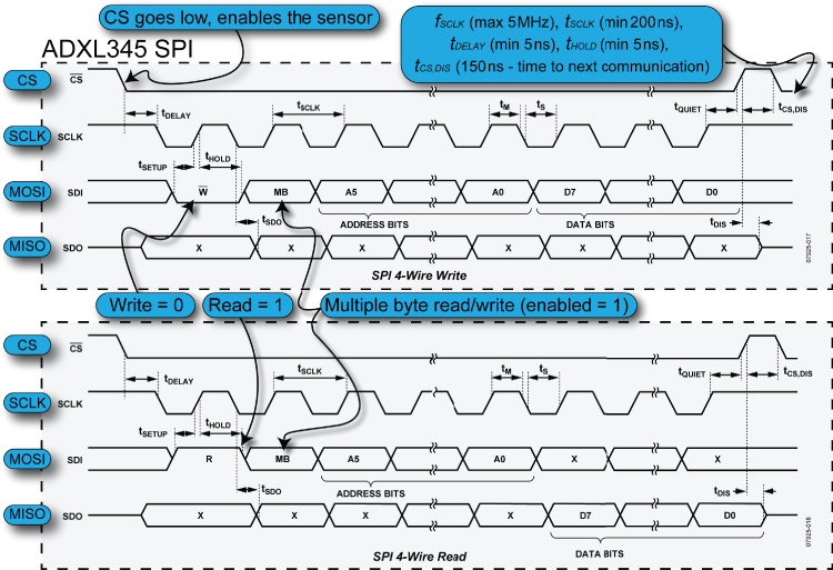
Figure 8-11: The ADXL345 SPI communication timing chart (from the ADXL345 datasheet)
Underlying image is courtesy of Analog Devices, Inc.
Note the following important points, which can be observed directly from the datasheet figure, as summarized in Figure 8-11:
- To write to an address, the first bit on the SDI line must be low. To read from an address, the first bit on the SDI line must be high.
- The second bit is called MB. From further analysis of the datasheet, this bit enables multiple byte reading/writing of the registers (i.e., send the first address and data will be continuously read from that register forward). This leaves six bits in the first byte for the address (26 = 6410 = 4016), which is sufficient to cover the available registers.
- As shown in Figure 8-11, the SCLK line is high at rest, and data is transferred on the rising edge of the clock signal. Therefore, the ADXL345 device must be used in communications mode 3 (refer to Table 8-3).
- When writing (top figure), the address (with a leading 0) is written to SDI, followed by the byte value to be written to the address.
- When reading (bottom figure), the address (with a leading 1) is written to SDI. A second byte is written to SDI and will be ignored. While the second (ignored) byte is being written to SDI, the response will be returned on SDO detailing the value stored at the register address.
Connecting the ADXL345 to the Beagle Boards
The ADXL345 breakout board can be connected to the SPI bus as illustrated in Figure 8-12(a), where MOSI on the BBB is connected to SDA and MISO is connected to SDO. The clock lines and the slave select lines are also interconnected. Figure 8-12(b) shows the equivalent connection for the PocketBeagle board.

Figure 8-12: (a) BBB SPI connection to the ADXL345, and (b) PocketBeagle SPI connection to the ADXL345
Once again, a logic analyzer is useful for debugging problems that can occur with SPI bus communication. For example, Figure 8-13 captures a read operation at address 0x00. You may notice that the value that was sent was 0x80 and not 0x00. This is because (as detailed in Figure 8-11) the leading bit must be a 1 to read and a 0 to write from/to an address. Sending 0x00 is a write request to address 0x00 (which is not possible), and sending 0x80 (i.e., 10000000 + 00000000) is a request to read the value at address 0x00. The second bit is 0 in both cases, thus disabling multiple-byte read functionality for this example.
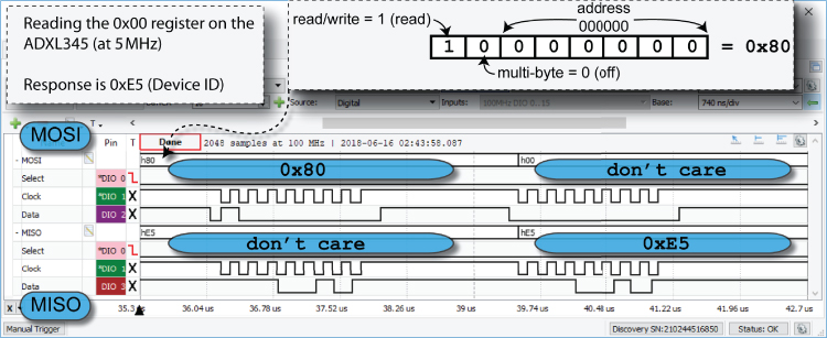
Figure 8-13: Reading the 0x00 register on the ADXL345 using SPI
The code in Listing 8-4 is adapted in /spi/spiADXL345/spiADXL345.c so that it reads the first register (0x00) of the ADXL345, which should return the DEVID, as illustrated in Figure 8-5. This value should be E516, which is 22910. The maximum recommended SPI clock speed for the ADXL345 is 5MHz, so this value is used in the program code.
debian@ebb:~/exploringbb/chp08/spi/spiADXL345$ gcc spiADXL345.c -o spiADXL345debian@ebb:~/exploringbb/chp08/spi/spiADXL345$ ./spiADXL345spi mode: 0x3bits per word: 8max speed: 5000000 Hz (5000 KHz)Return value: 229
Wrapping SPI Devices with C++ Classes
A C++ class is available in Listing 8-5 that wraps the software interface to the SPI bus, using the OOP techniques that are described in Chapter 5. This class is quite similar to the I2CDevice class that is described in Listing 8-2.
Listing 8-5: /chp08/spi/spiADXL345_cpp/SPIDevice.h
class SPIDevice {public:enum SPIMODE{ //!< The SPI ModeMODE0 = 0, //!< Low at idle, capture on rising clock edgeMODE1 = 1, //!< Low at idle, capture on falling clock edgeMODE2 = 2, //!< High at idle, capture on falling clock edgeMODE3 = 3 //!< High at idle, capture on rising clock edge};public:SPIDevice(unsigned int bus, unsigned int device);virtual int open();virtual unsigned char readRegister(unsigned int registerAddress);virtual unsigned char* readRegisters(unsigned int number, unsigned int fromAddress=0);virtual int writeRegister(unsigned int registerAddress, unsigned char value);virtual void debugDumpRegisters(unsigned int number = 0xff);virtual int write(unsigned char value);virtual int write(unsigned char value[], int length);virtual int setSpeed(uint32_t speed);virtual int setMode(SPIDevice::SPIMODE mode);virtual int setBitsPerWord(uint8_t bits);virtual void close();virtual ~SPIDevice();virtual int transfer(unsigned char read[], unsigned char write[], int length);private:std::string filename; //!< The precise filename for the SPI deviceint file; //!< The file handle to the deviceSPIMODE mode; //!< The SPI mode as per the SPIMODE enumerationuint8_t bits; //!< The number of bits per worduint32_t speed; //!< The speed of transfer in Hzuint16_t delay; //!< The transfer delay in usecs};
The SPI class in Listing 8-5 can be used in a stand-alone form for any SPI device type. For example, Listing 8-6 demonstrates how to probe the ADXL345 device.
Listing 8-6: /chp08/spi/spiADXL345_cpp/SPITest.cpp
#include <iostream>#include <sstream>#include "bus/SPIDevice.h"#include "sensor/ADXL345.h"using namespace std;using namespace exploringBB;int main(){SPIDevice spi(0,0);spi.setSpeed(5000000);cout << "The device ID is: " << (int) spi.readRegister(0x00) << endl;spi.setMode(SPIDevice::MODE3);spi.writeRegister(0x2D, 0x08);spi.debugDumpRegisters(0x40);}
This will give the following output when built and executed (0xE5 = 22910):
debian@ebb:~/exploringbb/chp08/spi/spiADXL345_cpp$ ./builddebian@ebb:~/exploringbb/chp08/spi/spiADXL345_cpp$ ./SPITestThe device ID is: 229SPI Mode: 3Bits per word: 8Max speed: 5000000Dumping Registers for Debug Purposes:e5 00 00 00 00 00 00 00 00 00 00 00 00 00 00 4a82 00 30 00 00 01 fe 08 00 00 00 ea 00 00 00 0000 00 00 00 00 00 00 00 00 00 00 00 0a 08 00 0002 0b 3a 00 db ff 17 01 00 00 00 00 00 00 00 00
The same SPIDevice class can be used as the basis for modifying the ADXL345 class in Listing 8-3 to support the SPI bus rather than the I2C bus. Listing 8-7 provides a segment of the class that is complete in the /chp08/spi/spiADXL345_cpp/ directory.
Listing 8-7: /chp08/spi/spiADXL345_cpp/ADXL345.h (Segment)
class ADXL345{public:enum RANGE { … };enum RESOLUTION { … };private:SPIDevice *device;unsigned char *registers;…public:ADXL345(SPIDevice *busDevice);virtual int readSensorState();…virtual void displayPitchAndRoll(int iterations = 600);virtual ~ADXL345();};
The full class from Listing 8-7 can be used to build an example, as in Listing 8-8. This example helps demonstrate how an embedded device that is attached to one of the buses can be wrapped with a high-level OOP class.
Listing 8-8: :/chp08/spi/spiADXL345_cpp/testADXL345.cpp
#include <iostream>#include <sstream>#include "bus/SPIDevice.h"#include "sensor/ADXL345.h"using namespace std;using namespace exploringBB;int main(){cout << "Starting EBB ADXL345 SPI Test" << endl;SPIDevice *busDevice = new SPIDevice(0,0);busDevice->setSpeed(5000000);ADXL345 acc(busDevice);acc.displayPitchAndRoll(100);cout << "End of EBB ADXL345 SPI Test" << endl;}
When this program is executed, it displays the current accelerometer pitch and roll values on a single line of the terminal window.
debian@ebb:~/exploringbb/chp08/spi/spiADXL345_cpp$ ./builddebian@ebb:~/exploringbb/chp08/spi/spiADXL345_cpp$ ./testADXL345Starting EBB ADXL345 SPI TestPitch:47.1902 Roll:-6.48042
Three-Wire SPI Communication
The ADXL345 supports a three-wire SPI (half duplex) mode. In this mode, the data is read and transmitted on the same SDIO line. To enable this mode on the ADXL345, the value 0x40 must be written to the 0x31 (DATA_FORMAT) register, and a 10kΩ resistor should be placed between SD0 and VCC on the ADXL345. There is a draft project in place in the chp08/spi/spiADXL345/3-wire/ directory, but at the time of writing, there is a lack of support for this mode in current Linux distributions.
Multiple SPI Slave Devices
One of the advantages of the SPI bus is that it can be shared with multiple slave devices, provided that only one slave device is active when communication takes place. On most microcontrollers, GPIO pins can be used as slave selection pins, and a similar structure can be developed for the Beagle boards. While the Debian image has kernel support for multiple slave selection pins on the SPI bus through entries in the /dev/ directory, it is not fully realized on the Beagle boards. The idea is that multiple devices (0 and 1) are associated with SPI1, and each is activated by using one of the following entries:
debian@ebb:/dev$ ls -l spidev1*crw-rw---- 1 root spi 153, 1 Jan 1 2000 spidev1.0crw-rw---- 1 root spi 153, 2 Jan 1 2000 spidev1.1
If you want to allow the Linux SPI interface library code to retain control of the slave selection functionality, then a wiring configuration similar to Figure 8-14 could be used. This configuration uses OR gates and an inverter to ensure that only one CS input is pulled low at a single time. In Figure 8-14 (a), the ADXL345 slave device is active when CS = 0 and GPIO = 0, and in Figure 8-14 (b), the second slave device is active when CS = 0 and GPIO = 1.
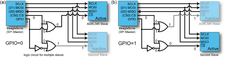
Figure 8-14: BBB control of more than one slave device using GPIO pins and additional logic
Depending on the particular slave devices being used, the GPIO output combined with a single inverter may be sufficient, as you could “permanently” pull the ![]() line low on the slave device, ignoring the CS output of the master. However, this would not work for the 74HC595 example, as the Beagle board's CS line is used to latch the data to the output LEDs.
line low on the slave device, ignoring the CS output of the master. However, this would not work for the 74HC595 example, as the Beagle board's CS line is used to latch the data to the output LEDs.
For more than two slave devices, a 3-to-8 line decoder, such as the 74HC138, would be a good solution. It has inverted outputs, which means that only one of its eight outputs is low at a single point in time. This device could be controlled using three of the board's GPIOs, and it could enable one of eight slave devices (23 = 8). There are also 4-to-16 line decoders with inverting outputs, such as the 74HC4515, which would enable you to control 16 slave devices with only four GPIOs (24 = 16). For both of these devices, the Beagle board's CS output could be connected to their ![]() enable input(s).
enable input(s).
UART
A Universal Asynchronous Receiver/Transmitter (UART) is a microprocessor peripheral device used for the serial transfer of data, one bit at a time, between two electronic devices. UARTs were originally stand-alone ICs but now are often integrated with the host microprocessor/microcontroller. A UART is not, strictly speaking, a bus, but its capacity to implement serial data communications overlaps with similar capacities of the I2C and SPI buses described earlier. A UART is described as asynchronous because the sender does not need to send a clock signal to the recipient to synchronize the transmission; rather, a communication structure is agreed upon that uses start and stop bits to synchronize the transmission of data. Because no clock is required, the data is typically sent using only two signal lines. Just like a regular telephone line, the transmit data connection (TXD) from one end is connected to the receive data connection (RXD) on the other end of the connection, and vice versa.
Traditionally, UARTs have been used with level converters/line drivers to implement interfaces such as RS-232 or RS-485, but for short-distance communications, it is possible to use the original logic level for the UART outputs and inputs to enable two UARTs to communicate with each other. Note that this is a perfectly possible but nonstandardized use of UARTS.
The number of symbols per second is known as the baud rate or modulation rate. With certain encoding schemes, a symbol could be used to represent two bits (i.e., four states, for example, by using quadrature phase-shift keying [QPSK]). Then the bit rate would be twice the baud rate. However, for a simple bi-level UART connection, the baud rate is the same as the bit rate.
The transmitter and receiver agree upon a bit rate before communication begins. The byte rate is somewhat lower than 1/8th of the bit rate, as there are overhead bits associated with the serial transmission of data. Transmission begins when the transmitter sends a start bit (logic low), as shown in Figure 8-15. On the receiver's end, the falling edge of the start bit is detected, and then after 1.5 bit periods, the first bit value is sampled. Every subsequent bit is sampled after 1.0 bit periods, until the agreed-upon number of bits is transferred (typically seven or eight). The parity bit is optional (though both devices must be configured to either use it or not); if used, it can identify whether a transmission error has occurred. It would be high or low, depending on whether odd or even parity checking is employed. Finally, one stop bit is sent (or optionally two stop bits), which is always a logic high value. The examples that follow in this section all use a standard 8N1 form, which means that eight bits are sent in each frame, with no parity bits and one stop bit.
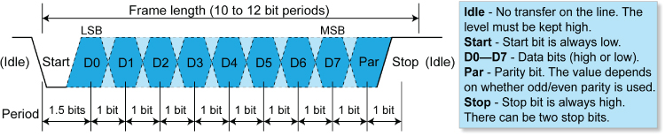
Figure 8-15: UART transmission format for a typical one-byte transfer
The Beagle Board UART
The Beagle boards each have four UARTs that are accessible via the GPIO Expansion headers at the pin locations listed in Table 8-5. In addition, UART3 is not broken out to the GPIO Headers.
Table 8-5: Beagle Board UART Header Pins (PocketBeagle in Brackets)
| UART0 | UART1 | UART2 | UART4 | UART5 | |
| TXD | n/a (P1.30) | P9_24 (P2.9) | P9_21 (P1.10) | P9_13 (P2.7) | P8_37 (n/a) |
| RXD | n/a (P1.32) | P9_26 (P2.11) | P9_22 (P1.8) | P9_11 (P2.5) | P8_38 (n/a) |
For the following examples UART4 is used. As detailed in Table 8-5, the pins for UART4 are as follows:
- UART4-TXD: P9_13 on the BeagleBone or P2.7 on the PocketBeagle. This is an output that transmits data to a receiver.
- UART4-RXD: P9_11 on the BeagleBone or P2.5 on the PocketBeagle. This is an input that receives data from a transmitter.
Chapter 9 describes how you can add additional UARTs to the Beagle boards using USB devices, but this chapter focuses on the built-in UART. The first test is to connect these two pins together, as in Figure 8-16(a), so that the board UART is literally “talking to itself.”
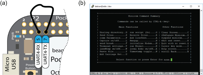
Figure 8-16: (a) Loopback testing the UART, and (b) configuring the minicom program settings
The /dev directory includes entries for ttyO0 to ttyO4 (letter O, not zero). This is the “teletype” (terminal) device, which is a software interface that enables you to send and receive data via the on-board UART. First, check that the terminal device is listed (on the PocketBeagle).
debian@ebb:/dev$ ls -l ttyO*lrwxrwxrwx 1 root root 5 Jan 1 2000 ttyO0 -> ttyS0lrwxrwxrwx 1 root root 5 Jan 1 2000 ttyO1 -> ttyS1lrwxrwxrwx 1 root root 5 Jan 1 2000 ttyO2 -> ttyS2lrwxrwxrwx 1 root root 5 Jan 1 2000 ttyO4 -> ttyS4
To test the device, you can use the agetty (alternative getty) command or the minicom terminal emulator, both of which enable you to send and receive data on the ttyO4 device. The minicom program enables you to dynamically change the serial settings while it is executing (e.g., number of bits in a frame, number of stop bits, parity settings) by pressing Ctrl+A followed by Z. Install and execute minicom using the following commands:
debian@ebb:/dev$ sudo apt install minicomdebian@ebb:/dev$ minicom -b 115200 -o -D /dev/ttyO4Welcome to minicom 2.7OPTIONS: I18nCompiled on Apr 22 2017, 09:14:19.Port /dev/ttyO4, 04:02:08Press CTRL-A Z for help on special keys
At this point, you should press Ctrl+A followed by Z and then E to turn on local Echo. Now when the board is wired as in Figure 8-16(a) and you press a key, you should see the following output when you type letters:
hheelllloo PPoocckkeettBBeeaaggllee Whichever key you press is transmitted in binary form (as in Figure 8-17) from the TXD output and is echoed on the console. When the character is received on the RXD input, it is then displayed on the terminal. Therefore, if you can see the characters appearing twice for the keys that you are pressing, then the simple UART test is working correctly. You can verify this by briefly disconnecting one end of the TXD-RXD loopback wire in Figure 8-16(a), whereupon the key presses will appear only once.

Figure 8-17: Logic analyzer display of the loopback serial transmission of the letter h (0x68) = 011010002 at 115,200 baud
The Analog Discovery has an interpreter that can be used for analyzing serial data communication. The logic analyzer can be connected in parallel to the TXD and RXD lines to analyze the transfer of data from the board to another device. An example of the resulting signals is displayed in Figure 8-17 for the loopback test in Figure 8-16(a) when only the letter “h” is being transmitted. The start and stop bits can be observed, along with the eight-bit data as it is sent, LSB first, from the TXD pin to the RXD pin, with a sample bit-period of 8.7μs. At a baud rate of 115,200, the effective byte rate will be somewhat lower because of the overhead of transmitting start, stop, and parity bits.
To this point, this chapter describes SPI and I2C communication as well as UART. However, using a UART connection is probably the most straightforward approach, and it has the additional advantage that there can be some degree of physical distance between the two controllers. Table 8-6 lists some advantages and disadvantages of using a UART in comparison to using I2C or SPI.
Table 8-6: Advantages and Disadvantages of UART Communication
| ADVANTAGES | DISADVANTAGES |
| Simple, single-wire transmission and single-wire reception of data with error checking. | The typical maximum data rate is low compared to SPI (typically 460.8kb/sec). |
| Easy interface for interconnecting embedded devices and desktop computers, etc., especially when that communication is external to the device and/or over a significant distance—some tens of feet. I2C and SPI are not suited for external/distance communication. | Because it is asynchronous, the clock on both devices must be accurate, particularly at higher baud rates. You should investigate Controller Area Network (CAN) buses for high-speed external asynchronous data transfer (described later in this chapter). |
| Can be directly interfaced to popular RS-232 physical interfaces, enabling long-distance communication (15 meters or greater). The longer the cable, the lower the speed. RS-422/485 allows for 100-meter runs at greater than 1Mb/s. | UART settings need to be known in advance of the transfer, such as the baud rate, data size, and parity checking type. |
UART Examples in C
The next step is to write C code on the board that can communicate with the desktop computer using the USB-to-TTL 3.3V cable (see Chapter 2), as wired in Figure 8-19(a). You should first test your connection by opening a serial terminal connection on the desktop PC (e.g., using PuTTY) and then use minicom on the Beagle board to communicate with the desktop PC.
Beagle Board Serial Client
The C program in Listing 8-9 sends a string to a desktop machine (or any other device) that is listening to the other end of the connection (e.g., using PuTTY). It uses the Linux termios library, which provides a general terminal interface that can control asynchronous communication ports.
Listing 8-9: exploringbb/chp08/uart/uartC/uart.c
#include<stdio.h>#include<fcntl.h>#include<unistd.h>#include<termios.h>#include<string.h>int main(int argc, char *argv[]){int file, count;if(argc!=2){printf("Please pass a message string to send, exiting! ");return -2;}if ((file = open("/dev/ttyO4", O_RDWR | O_NOCTTY | O_NDELAY))<0){perror("UART: Failed to open the device. ");return -1;}struct termios options;tcgetattr(file, &options);options.c_cflag = B115200 | CS8 | CREAD | CLOCAL;options.c_iflag = IGNPAR | ICRNL;tcflush(file, TCIFLUSH);tcsetattr(file, TCSANOW, &options);// send the string plus the null characterif ((count = write(file, argv[1], strlen(argv[1])+1))<0){perror("UART: Failed to write to the output. ");return -1;}close(file);printf("Finished sending the message, exiting. ");return 0;}
This code uses the termios structure, setting flags to define the type of communication that should take place. The termios structure has the following members:
tcflag_t c_iflag: Sets the input modestcflag_t c_oflag: Sets the output modestcflag_t c_cflag: Sets the control modestcflag_t c_lflag: Sets the local modescc_t c_cc[NCCS]: Used for special characters
A full description of the termios functionality and flag settings is available by typing man termios at the Linux shell prompt.
debian@ebb:~/exploringbb/chp08/uart/uartC$ gcc uart.c -o uart…/exploringbb/chp08/uart/uartC$ ./uart "Hello Desktop!"Finished sending the message, exiting.…/exploringbb/chp08/uart/uartC$ ./uart " From the PocketBeagle."Finished sending the message, exiting.…/exploringbb/chp08/uart/uartC$ echo " Using echo!" >> /dev/ttyO4
The output appears on the desktop PC as in Figure 8-18 when PuTTY is set to listen to the correct serial port (e.g., COM5 in my case). The C program functionality is similar to a simple echo to the terminal device; however, it does have access to set low-level modes such as the baud rate, parity types, and so on.
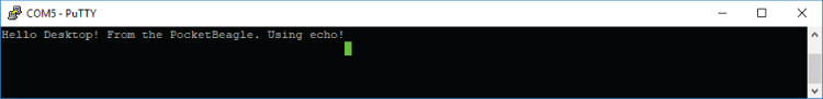
Figure 8-18: A PuTTY desktop COM terminal that is listening for messages from the Beagle board
LED Serial Server
For some applications, it can be useful to allow a desktop computer master to take control of a Beagle board slave. In this section, a serial server runs on the PocketBeagle and awaits commands from a desktop serial terminal. Once again, the USB-to-TTL 3.3V cable is used; however, it is important to note that a similar setup could be developed with wireless technologies, such as Bluetooth, infrared transmitter/receivers, and serial ZigBee (see Chapter 12).
In this example, the PocketBeagle is connected to a simple LED circuit and the USB-to-TTL cable, as illustrated in Figure 8-19(a). When the PuTTY client on the desktop computer issues simple string commands such as LED on and LED off, as illustrated in Figure 8-19(b), the hardware LED that is attached to the board performs a corresponding action. Importantly, this program permits safe remote control of the board, as it does not allow the serial client access to any other functionality on the board—in effect, the serial server behaves like a shell that has only three commands! Please note that you may have to turn on local echo in the terminal window (e.g., in PuTTY use Terminal → Local echo and select the option “Force on”).

Figure 8-19: (a) The LED serial server circuit, and (b) PuTTY on the PC communicating to the LED serial server
The source code for the serial server is provided in Listing 8-10. The example uses sysfs to control the LED circuit (see Chapter 5). On execution, the server displays the following output when you provide the input strings that are captured in Figure 8-19(b):
debian@ebb:~/exploringbb/chp08/uart/server$ gcc server.c -o serverdebian@ebb:~/exploringbb/chp08/uart/server$ ./serverEBB Serial Server runningLED onServer>>>[Turning the LED on]LED offServer>>>[Turning the LED off]quitServer>>>[goodbye]
You can then add a new service entry for the server code in this section so that it starts on boot. If your intention is to run this program as a service, then you should, of course, remove the client-controlled “quit” functionality!
Listing 8-10: /exploringbb/chp08/uart/server/server.c
#include<stdio.h>#include<fcntl.h>#include<unistd.h>#include<termios.h>#include<string.h>#include<stdlib.h>#define LED_PATH "/sys/class/gpio/gpio60/"// Sends a message to the client and displays the message on the consoleint message(int client, char *message){int size = strlen(message);printf("Server>>>%s ", (message+1)); // print message with new lineif (write(client, message, size)<0){perror("Error: Failed to write to the client ");return -1;}write(client, " EBB>", 7); // display a simple promptreturn 0; // for a carriage return}void makeLED(char filename[], char value[]){FILE* fp; // create a file pointer fpchar fullFileName[100]; // to store the path and filenamesprintf(fullFileName, LED_PATH "%s", filename); // write path and filenamefp = fopen(fullFileName, "w+"); // open file for writingfprintf(fp, "%s", value); // send the value to the filefclose(fp); // close the file using the file pointer}// Checks to see if the command is one that is understood by the serverint processCommand(int client, char *command){int val = -1;if (strcmp(command, "LED on")==0){val = message(client, " [Turning the LED on]");makeLED("value", "1"); // turn the physical LED on}else if(strcmp(command, "LED off")==0){val = message(client, " [Turning the LED off]");makeLED("value", "0"); // turn the physical LED off}else if(strcmp(command, "quit")==0){ // shutting down server!val = message(client, " [goodbye]");}else { val = message(client, " [Unknown command]"); }return val;}int main(int argc, char *argv[]){int client, count=0;unsigned char c;char *command = malloc(255);makeLED("direction", "out"); // the LED is an outputif ((client = open("/dev/ttyO4", O_RDWR | O_NOCTTY | O_NDELAY))<0){perror("UART: Failed to open the file. ");return -1;}struct termios options;tcgetattr(client, &options);options.c_cflag = B115200 | CS8 | CREAD | CLOCAL;options.c_iflag = IGNPAR | ICRNL;tcflush(client, TCIFLUSH);fcntl(STDIN_FILENO, F_SETFL, O_NONBLOCK); // make reads non-blockingtcsetattr(client, TCSANOW, &options);if (message(client, " EBB Serial Server running")<0){perror("UART: Failed to start server. ");return -1;}// Loop forever until the quit command is sent from the client or// Ctrl-C is pressed in the server's terminal windowdo {if(read(client,&c,1)>0){write(STDOUT_FILENO,&c,1);command[count++]=c;if(c==' '){command[count-1]='�'; // replace /n with /0processCommand(client, command);count=0; // reset the command string}}if(read(STDIN_FILENO,&c,1)>0){ // can send from stdin to clientwrite(client,&c,1);}}while(strcmp(command,"quit")!=0);close(client);return 0;}
UART Applications: GPS
A low-cost Global Positioning System (GPS) module has been chosen as an example device to demonstrate interconnection to Beagle board UART devices. The GY-GPS6MV2 breakout board (~$10) uses the u-blox NEO-6M series GPS module (tiny.cc/beagle804). It can be powered at 3.3V and therefore can be connected directly to a Beagle board's UART pins.
Figure 8-20 illustrates the board UART connection to the GPS module. As with all UART connections, ensure that you connect the transmit pin of the board to the receive pin of the device and connect the receive pin of the board to the transmit pin of the device.
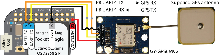
Figure 8-20: PocketBeagle UART connection to the GPS module
The GPS module is set for 9600 baud by default, so to connect to the module, you can use the following:
debian@ebb:~$ sudo minicom -b 9600 -o -D /dev/ttyO4Welcome to minicom 2.7OPTIONS: I18nCompiled on Apr 22 2017, 09:14:19.Port /dev/ttyO4, 23:40:20Press CTRL-A Z for help on special keys$GPRMC,133809.00,A,5323.12995,N,00615.36410,W,1.015,,190815,,,A*60$GPVTG,,T,,M,1.015,N,1.879,K,A*21$GPGGA,133809.00,5323.12995,N,00615.36410,W,1,08,1.21,80.2,M,52.9,M,,*73$GPGSA,A,3,21,16,18,19,26,22,07,27,,,,,2.72,1.21,2.44*06$GPGSV,4,1,14,04,07,227,17,07,24,306,16,08,33,278,09,13,05,018,*7A$GPGSV,4,2,14,15,04,048,08,16,61,174,25,18,39,096,31,19,35,275,21*78$GPGSV,4,3,14,20,12,034,08,21,36,061,23,22,29,142,21,26,32,159,12*71$GPGSV,4,4,14,27,75,286,26,30,10,334,*75$GPGLL,5323.12995,N,00615.36410,W,133809.00,A,A*78
The GPS module outputs NEMA 0183 sentences, which can be decoded to provide information about the sensor's position, direction, velocity, and so on. There is a lot of work involved in decoding the sentences, so it is best to use a client application to test the performance of your sensor. Here's an example:
debian@ebb:~$ sudo apt install gpsd-clientsdebian@ebb:~$ gpsmon /dev/ttyO4
This results in the output shown in Figure 8-21 that provides an intuitive display of the NEMA 0183 sentences. An LED on the module flashes at a rate of 1 pulse per second (PPS) when it is capturing valid data. This pulse is extremely accurate and can therefore be used as a calibration method for other applications. The gpsmon application was executed in my office, which overlooks a courtyard, so I was surprised that the low-cost sensor achieved line of sight with 11 satellites.

Figure 8-21: The gpsmon output display
Walter Dal Mut (@walterdalmut) has made a C library available for interfacing to GPS sensors. The library can be easily integrated within your project to utilize GPS, as follows:
debian@ebb:~$ git clone git://github.com/wdalmut/libgpsCloning into 'libgps'…debian@ebb:~$ cd libgpsdebian@ebb:~/libgps$ make/usr/bin/make -C src allRUN TESTS SHOULD BE A GOOD IDEA…make tests…debian@ebb:~/libgps$ sudo make installdebian@ebb:~/libgps$ ls /usr/lib/libgps.a/usr/lib/libgps.a
Once the library has been installed, you can use a straightforward C program to identify the GPS information, as in Listing 8-11.
Listing 8-11: /exploringbb/chp08/uart/gps/gps_test.c
#include<stdio.h>#include<stdlib.h>#include<gps.h>int main() {gps_init(); // initialize the deviceloc_t gps; // a location structuregps_location(&gps); // determine the location dataprintf("The board location is (%lf,%lf) ", gps.latitude, gps.longitude);printf("Altitude: %lf m. Speed: %lf knots ", gps.altitude, gps.speed);return 0;}
You can build and execute the code as follows:
…/exploringbb/chp08/uart/gps$ gcc gps_test.c -o gps_test -lgps -lm…/exploringbb/chp08/uart/gps$ ./gps_testThe board location is (53.385511,-6.256224)Altitude: 81.900000 m. Speed: 0.060000 knots
You can enter the coordinate pair in maps.google.com to find my office at Dublin City University (tiny.cc/beagle805)!
CAN Bus
Controller Area Network (CAN) was developed by Bosch for industrial communication applications. Similar to I2C, CAN supports multimaster messaging at rates of up to 1MB/sec. Unlike the other buses described in this chapter, CAN uses short messages called frames, as illustrated in Figure 8-22. These frames have an identifier that allows for priority messaging on the bus, where a lower value has the highest message priority. There are four frame types.
- Data Frame is a regular data transmission frame.
- Remote Frame is a request for transmission from another node.
- Error Frame is used when an error occurs (such as an incorrect checksum) and causes the original transmitter to resend the message.
- Overload Frame is used when a node is too busy. It inserts a delay into communications between each frame to give the node time to process.

Figure 8-22: A standard CAN frame (extended CAN frames are also available that have an additional 18-bit identifier extension)
CAN is designed primarily for distributed real-time control, particularly where security, cost, low latency, and high-error failsafe are important design criteria. As a result, CAN is used today in automotive and industrial control. CAN supports CSMA/CD+AMP, which means
- Carrier sense/multiple access (CSMA) allows a bus participant to wait for inactivity before a message is sent. Even with such sensing, two participants could begin transmitting at the same time.
- Collision detection with arbitration on message priority (CD + AMP) uses bitwise arbitration, where each participant places a frame on the bus bit -by bit and then checks its values. Higher-priority messages always win bus access, as the first bits to be transmitted in the frame represent the identifier.
The buses described to this point in the chapter use single-ended signals, where a signal is sent on a data line and has a return path through GND. The CAN bus uses a differential communications model, where balanced signals are used to transmit the signal, as illustrated in Figure 8-23(a). Noise as a result of electromagnetic interference (EMI) is likely to affect both lines equally and is therefore canceled out. Differential signaling is also used in USB and Ethernet communications as it gives better signal voltage versus power consumption than single-ended communications.

Figure 8-23: (a) Single-ended versus differential communications, and (b) voltage levels used in CAN bus signaling for 5V CAN (3.3V CAN is typically centered around 2.3V)
Figure 8-23(b) illustrates the voltage levels used in 5V CAN bus signaling, where a dominant bit (a logic low) is transmitted by setting the CAN_H line to ~3.5V and the CAN_L line to ~1.5V. When the bus is idle, the bit is recessive (a logic high), and the line voltages are both weakly biased at approximately 2.5V.
Beagle Board CAN Bus
The AM335x SoC has a DCAN controller that provides two CAN bus devices (DCAN0 and DCAN1), which are accessible through the Expansion Headers as described in Table 8-7. The DCAN controller supports CAN protocol version 2.0 (A and B) at bit rates of up to 1Mbit/s. You will need to add CAN transceiver (transmitter and receiver) hardware to your Beagle board to drive the physical layer voltage levels, which are illustrated in Figure 8-23(b). Modules that use the TI SN65HVD230 CAN Bus Transceiver IC are popular for this task (tiny.cc/beagle810) as they operate at 3.3V logic levels, support data rates of up to 1Mbit/s, and are available in modular form for as little as $1 each.
Table 8-7: CAN Bus Pins on the Beagle Boards (All Mux Mode 2)
| H/W BUS | POCKETBEAGLE | BEAGLEBONE |
| CAN0 RX |
P1.28 or P1.30
|
P9_19 |
| CAN0 TX |
P1.26 or P1.32
|
P9_20 |
| CAN1 RX |
P2.09 or P2.25
|
P9_24 |
| CAN1 TX |
P2.11 or P2.27
|
P9_26 |
SocketCAN
Linux provides support for CAN through the networking subsystem and SocketCAN. SocketCAN is a hardware-independent CAN API that allows for multiuser userspace control of CAN devices. The advantage of this design is that users can easily write program code that typically sends and receives raw CAN frames to and from the bus. The downside is that this approach uses a full-stack networking approach for a bus that was designed for low-latency and that the packet scheduler is shared with other buses (e.g., heavy network traffic on Ethernet). You can configure the pins for DCAN0 as follows:
debian@ebb:~$ config-pin -q P1.28P1_28 Mode: default Direction: in Value: 0debian@ebb:~$ config-pin -q P1.26P1_26 Mode: default Direction: in Value: 0debian@ebb:~$ config-pin P1.28 candebian@ebb:~$ config-pin P1.26 candebian@ebb:~$ config-pin -q P1.28P1_28 Mode: candebian@ebb:~$ config-pin -q P1.26P1_26 Mode: can
and DCAN1 as follows:
debian@ebb:~$ config-pin P2.9 candebian@ebb:~$ config-pin P2.11 candebian@ebb:~$ config-pin -q P2.9P2_09 Mode: candebian@ebb:~$ config-pin -q P2.11P2_11 Mode: can
Load the LKMs for CAN (it is likely that only the last module is required) and then check that the LKM loaded correctly.
debian@ebb:~$ dmesg|grep can[ 1.210665] c_can_platform 481cc000.can: c_can_platform deviceregistered (regs=fa1cc000, irq=39)[ 1.211749] c_can_platform 481d0000.can: c_can_platform deviceregistered (regs=fa1d0000, irq=40)[ 1.328253] can: controller area network core (rev 20170425 abi 9)debian@ebb:~$ sudo modprobe candebian@ebb:~$ sudo modprobe can-devdebian@ebb:~$ sudo modprobe can-rawdebian@ebb:~$ lsmod|grep cancan_raw 20480 0debian@ebb:~$ dmesg|grep raw[ 625.214610] can: raw protocol (rev 20170425)
The CAN Bus devices can then be brought up as follows, where a bit rate of 125Kbit/s is specified (this value can be as high as 1,000,000—i.e., 1Mbit/s):
debian@ebb:~$ sudo ip link set can0 up type can bitrate 125000debian@ebb:~$ sudo ip link set can1 up type can bitrate 125000debian@ebb:~$ sudo ifconfig can0 updebian@ebb:~$ sudo ifconfig can1 updebian@ebb:~$ ifconfigcan0: flags=193<UP,RUNNING,NOARP> mtu 16unspec 00-00-00-00-00-00-00-00-00-00-00-00-00-00-00-00…device interrupt 39can1: flags=193<UP,RUNNING,NOARP> mtu 16unspec 00-00-00-00-00-00-00-00-00-00-00-00-00-00-00-00…device interrupt 40…debian@ebb:~$ ip -details link show can02: can0: <NO-CARRIER,NOARP,UP,ECHO> mtu 16 qdisc pfifo_fast state DOWNmode DEFAULT group default qlen 10link/can promiscuity 0can state BUS-OFF (berr-counter tx 248 rx 0) restart-ms 0bitrate 125000 sample-point 0.875 …debian@ebb:~$ dmesg[ 727.310927] c_can_platform 481cc000.can can0: setting BTR=1c0b BRPE=0000[ 727.319229] IPv6: ADDRCONF(NETDEV_CHANGE): can0: link becomes ready[ 822.875931] c_can_platform 481d0000.can can1: setting BTR=1c0b BRPE=0000[ 822.883165] IPv6: ADDRCONF(NETDEV_CHANGE): can1: link becomes ready
A CAN Bus Test Circuit
You can use both CAN buses on the PocketBeagle or BeagleBone to create a true hardware loopback test. You could also perform this test by using one CAN interface on two separate boards. Importantly, you will need to acquire and connect two CAN physical layer modules (e.g., TI SN65HVD230-based modules), as illustrated in Figure 8-24. Other third-party CAN bus devices can be added to the bus at this point.
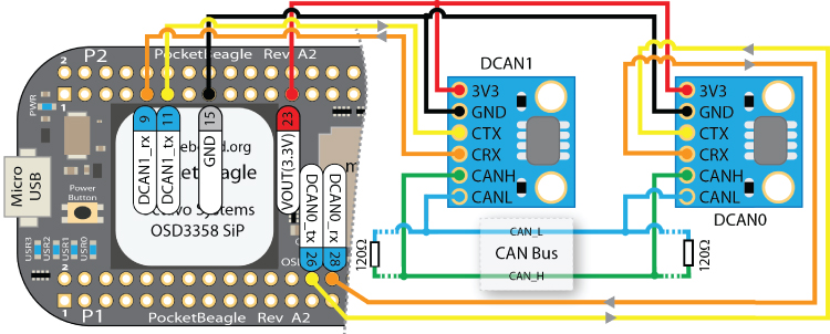
Figure 8-24: PocketBeagle CAN Bus test using DCAN0 and DCAN1 for a hardware loopback test with SN65HVD230 CAN modules
CAN Bus requires termination resistors on the CAN_H and CAN_L lines that match the nominal impedance of the cable. The ISO 11898 CAN standard requires a cable with a nominal impedance of 120Ω. You should place two such resistors on each end of the cable, as illustrated in Figure 8-24.
The device properties are available in /sysfs/ and /proc/ at the following locations:
debian@ebb:~$ ls /sys/class/net/can0 can1 lo usb0 usb1debian@ebb:~$ ls /sys/class/net/can0/addr_assign_type dormant name_assign_type speedaddress duplex netdev_group statisticsaddr_len flag operstate subsystem …debian@ebb:~$ cat /proc/net/can/versionrev 20170425 abi 9debian@ebb:~$ cat /proc/net/can/stats0 transmitted frames (TXF)0 received frames (RXF) …
Linux CAN-utils
You can test the configuration in Figure 8-24 using the SocketCAN Can-utils tools (elinux.org/Can-utils). These are installed on the BeagleBoard.org Linux image by default in the /usr/bin/ directory.
debian@ebb:/usr/bin$ ls can*canbusload candump cangen canlogserver cansendcan-calc-bit-timing canfdtest cangw canplayer cansniffer
The cansend utility can be used to send messages to the CAN bus. You can specify the CAN device (e.g., can0) followed by the CAN ID and data payload in the form <can_id>#<data>.
debian@ebb:~$ cansend can1 123#11.22.33.44.55.66.77.88debian@ebb:~$ cansend can0 123#11.22.33
The candump utility can be used to read messages from the bus. If you open two terminal windows (one for each CAN device) and run the candump utility in each window, you will see the following output when the cansend command is called:
debian@ebb:~$ candump can0can0 123 [8] 11 22 33 44 55 66 77 88can0 123 [3] 11 22 33debian@ebb:~$ candump can1can1 123 [8] 11 22 33 44 55 66 77 88can1 123 [3] 11 22 33debian@ebb:~$ cat /proc/net/can/stats42 transmitted frames (TXF)84 received frames (RXF)32 matched frames (RXMF) …
A large number of messages is typically sent to an active bus, so the candump utility also supports filters, which enables you to receive only frames in a particular range. For example, to receive all frames between 0x100 and 0x2FF, use this:
debian@ebb:~$ candump can0,100:2FF Figure 8-25 displays a capture of the CAN Bus in Figure 8-24 when the following message is transmitted to the bus. You can also see that the voltage level profile of the bus is consistent with Figure 8-23(b).5

Figure 8-25: A logic analyzer and scope capture of the CAN Bus circuit in Figure 8-24 sending the message 123#11.22.33.44.55.66.77.88
debian@ebb:~$ cansend can0 123#11.22.33.44.55.66.77.88 A SocketCAN C Example
SocketCAN greatly simplifies the complexity of the code that is required to read and write CAN frames to the bus. It uses the same framework as is used for TCP/IP socket communication, except that the protocol family is PF_CAN and the packet is sent using the raw interface. A modified version of the standard SocketCAN example from the SocketCAN Wikipedia page (en.wikipedia.org/wiki/SocketCAN) is presented in Listing 8-12 for convenience.
Listing 8-12: /chp08/can/simpleCAN.c
#include <stdio.h>#include <stdlib.h>#include <unistd.h>#include <string.h>#include <net/if.h>#include <sys/types.h>#include <sys/socket.h>#include <sys/ioctl.h>#include <linux/can.h>#include <linux/can/raw.h>int main(void) {int s, nbytes;struct sockaddr_can addr;struct can_frame frame;struct ifreq ifr;const char *ifname = "can0";if((s = socket(PF_CAN, SOCK_RAW, CAN_RAW)) < 0) {perror("Error while opening socket");return -1;}strcpy(ifr.ifr_name, ifname);ioctl(s, SIOCGIFINDEX, &ifr);addr.can_family = AF_CAN;addr.can_ifindex = ifr.ifr_ifindex;printf("%s at index %d ", ifname, ifr.ifr_ifindex);if(bind(s, (struct sockaddr *)&addr, sizeof(addr)) < 0) {perror("Error in socket bind");return -2;}frame.can_id = 0x123; // can0 123#11.22.33frame.can_dlc = 3;frame.data[0] = 0x11;frame.data[1] = 0x22;frame.data[2] = 0x33;nbytes = write(s, &frame, sizeof(struct can_frame));printf("Wrote %d bytes ", nbytes);return 0;}
The code can be compiled and executed as follows, whereupon a message will be sent to the bus and received by the candump utility that is running in a separate terminal window, provided that the circuit is configured as in Figure 8-24.
debian@ebb:~/exploringbb/chp08/can$ gcc simpleCAN.c -o simpledebian@ebb:~/exploringbb/chp08/can$ ./simplecan0 at index 2Wrote 16 bytesdebian@ebb:~$ candump can0can0 123 [3] 11 22 33
Logic-Level Translation
As noted throughout this chapter, it is important that you are cognizant of the voltage levels used in communicating with the Beagle boards. If you connect a device that uses 5V logic levels, then when the device is sending a high state to the board, it will apply a voltage of 5V to the board's input pins. This would likely permanently damage the board. Many embedded systems have overvoltage-tolerant inputs, but the Beagle boards do not. Therefore, logic-level translation circuitry is required if you want to connect the buses to 5V or 1.8V logic-level circuits.
For unidirectional data buses, like four-wire SPI, logic-level translation can be achieved using a combination of diodes (using their ~0.6V forward-voltage drop characteristic) combined with resistors, or transistors. However, bidirectional data buses like the I2C bus are more complex because the level must be translated in both directions on a single line. This requires circuits that use devices such as N-channel MOSFETs (e.g., the BSS138). They are available in surface-mounted packages and, unfortunately, there are few through-hole alternatives. Fortunately, this is a common problem, and there are straightforward unidirectional and bidirectional breakout board solutions available from several suppliers, including the following:
- SparkFun Bi-directional Logic Level Converter (BOB-12009), which uses the BSS138 MOSFET (~$3).
- Adafruit Four-Channel Bi-directional Level Shifter (ID:757), which uses the BSS138 MOSFET (1.8V to 10V shifting) (~$4).
- Adafruit Eight-Channel Bi-directional Logic Level Converter (ID:395; ~$8), which uses the TI TXB0108 Voltage-Level Translator that automatically senses direction (1.2–3.6V or 1.65–5.5V translation). Note that it does not work well with I2C because of the pull-up resistors required. However, it can switch at frequencies greater than 10MHz.
- Watterott Four-Channel Level Shifter (20110451), which uses the BSS138 MOSFET (~$2).
Some of these products are displayed in Figure 8-26. With the exception of the Adafruit eight-channel converter, they all use BSS138 MOSFETs. A small test was performed to check the switching frequency of these devices, as displayed in Figure 8-27, and it is clear from the oscilloscope traces that there are data-switching performance limitations when using these devices that you must factor into your circuit design. In this test, the 3.3V input is switching a 5V level output using a square wave, and it is clear that the output signal is distorted at higher frequencies. For example, when switching at 1MHz, the distortion means that the output signal does not actually reach a 5V level.
Figure 8-26: Adafruit four-channel, Adafruit eight-channel, and Watterott four-channel logic-level translators
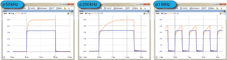
Figure 8-27: Switching BSS138-based translators from 3.3V to 5V logic levels at 50 kHz, 200kHz, and 1MHz
For further information on logic-level shifting techniques in I2C-bus design, see the application notes from NXP (AN97055), which are linked on the chapter web page and also available at tiny.cc/beagle806.
Summary
After completing this chapter, you should be able to do the following:
- Describe the most commonly used buses or interfaces that are available on the Beagle boards and choose the correct bus to use for your application
- Configure the Beagle boards to enable I2C, SPI, CAN bus, and UART capabilities
- Attach circuits to a Beagle board that interface to its I2C bus and use the Linux I2C-tools to communicate with those circuits
- Build circuits that interface to the SPI bus using shift registers and write C code that controls low-level SPI communication
- Write C/C++ code that interfaces to and “wraps” the functionality of devices attached to the I2C and SPI buses
- Communicate between UART devices using both Linux tools and custom C code
- Build a basic distributed system that uses UART connections to the board to allow it to be controlled from a desktop PC
- Interface to a low-cost GPS sensor using a UART connection
- Build circuits that interface to the Beagle board CAN buses and use Linux SocketCAN to send and receive messages to and from the bus
- Add logic-level translation circuitry to your circuits to communicate between devices with different logic-level voltages
Further Reading
Documents and links for further reading have been listed throughout this chapter, but here are some further reference documents:
- The I2C Manual, Jean-Marc Irazabal and Steve Blozis, Philips Semiconductors, TecForum at DesignCon 2003 in San Jose, CA, on January 27, 2003, at
tiny.cc/beagle807 - The Linux I2C Subsystem, at
i2c.wiki.kernel.org - Serial Programming Guide for POSIX Operating Systems, 5th ed., Michael R. Sweet, 1994–1999, at
tiny.cc/beagle808 - Serial Programming HOWTO, Gary Frerking, Revision 1.01, at
tiny.cc/beagle809