
The three-phase AC/AC matrix converters have attracted lots of interest in the 1990s [1,2,3,4,5,6,7]. Methods for both the realization of bidirectional switch and the PWM control have been investigated and most of the initial limitations of the matrix converter are nowadays overcome. This continuous effort has been rewarded with system-level products like Yaskawa Matrix Converter or power modules from manufacturers like Infineon, Semelab, Dynex or IXYS.
The Yaskawa’s AC7 Matrix Converter [8] represents the world’s first low voltage (230 V/460 V) matrix converter to directly convert input AC voltage to output AC voltage without the need for a DC Bus. Using this configuration helps improve energy efficiency and it also overcomes many problems typically associated with conventional drives such as harmonic current distortion, line regeneration, installation space, or motor drive issues with very long cable lengths, bearing currents, and common mode currents. This product line is rated up to 7.5 HP, 15 HP, 30/40 HP, with possible extension to 125HP, and it is recommended for applications like centrifuges, elevators, escalators or various test stands. A second product line is offered by Yaskawa Corporation to the European market as Varispeed F7.
Despite the academic success concerning the implementation of the matrix converters [9,10,11], it is worth noting that the Yaskawa Corporation changed the name of all its products in 2007 from names ending in the generation number like …“G7,” and so on, into names with 1000s like A2000. They changed all these names except for the Varispeed AC Drive based on matrix converters. These are still shown in the product line-up but they do not show in the annual financial report for 2011–2012 as a separate sales line as it was in 2004–2006. It does not seem that this is a representative or sellable product anymore. Moreover, the Medium Voltage (1000s of Volts) version of the matrix converter made by Yaskawa Corporation was only a one-time success for a skin mill corporation [12].
Another Japanese manufacturer, Fuji brought up to production a matrix converter series called Frenic-MX in 2006. Most of the other manufacturers have designed matrix converters for demonstration purposes, without finding enough benefits and customer appreciation to really replace (or complete) conventional back-to-back topologies with matrix converters within their product line.
Merits are proven usually in space and volume challenged applications like aviation systems [13,14,15]. Hence, a good opportunity for project development came along the All Electric Aircraft concept.
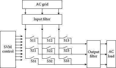
FIGURE 16.1 Basic matrix converter topology.
The academic interest for matrix converter topologies has fuelled industrial research, and power semiconductor manufacturers came up with integrated modules for implementation of the power stage suitable to a matrix converter.
The conventional AC/AC matrix converter is a matrix of switches that allows an independent control of frequency, amplitude, and phase of the outputs while the operation is synchronized with the input AC waveforms for operation with controllable displacement power factor (Figure 16.1).
Since three-phase systems are most commonly used, the matrix dimension is herein limited to three. Given all connection possibilities, the three-phase AC–AC matrix converter consists of nine bidirectional switches which allow an output terminal to be connected to any input terminal. Any symmetrical three-phase output voltages can be obtained from a set of input voltages by suitable switching of the matrix. The PWM operation of the switches requires that three voltage sources (or capacitors) are present on only one side to provide bypass paths for the inductive currents. Since the input AC source is conventionally an industrial or residential power grid, with a strong voltage source character, the output side will produce a voltage source character towards the load.
The load current is reflected towards the grid through switches into a pulsed current. When the pulsations of this current poses a problem to the grid, an input LC filter is required. The matrix converter will act as a current-type load, extracting current from the filter’s capacitor. In most cases, this capacitor will have its voltage uncontrolled by a feedback loop, and this should be considered in the protection circuitry.
The three-phase AC load can be a motor drive or a power supply load. In either case, the load should present an inductive character towards the power converter. For instance, a three-phase AC power supply will have a three-phase LC filter on the output side to provide the required inductive load character to the converter. Moreover, only one of the switches linked to the same output terminal can be in conduction at a given time. This means there are 27 possibilities of input-to-output connection (Figure 16.2):
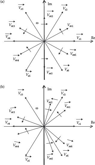
FIGURE 16.2 Possible space vector positions within the complex plane on the load-side reference frame when considering both stationary and rotating vectors: different moments captured in (a) and (b).
• Six possibilities to connect each output terminal to a different input terminal; these are equally 2π/3 out of phase, and each can be represented by a space vector rotating in the complex plane of the load reference frame (let us call them as “rotating vectors”).
• Eighteen possibilities to connect two output nodes to the same input terminal while the third output is linked to a different input. The matrix converter could be seen as a functional superposition of three three-phase inverters supplied by rectified line voltages. The appropriate switching vectors are fixed in six directions equally π/3 out of phase over the complex plane of the load reference frame and their magnitudes are variables as the rectified voltages evolve (let us call these vectors “stationary vectors”).
• Three null-states when all three output nodes are connected to the same input terminal.
Designing a PWM algorithm means averaging in between the available states in order to emulate a rotating vector in the load reference frame. Various methods are hence available.
16.2 IMPLEMENTATION OF THE POWER SWITCH
The most important hardware challenge relates to the implementation of the bi-directional power switch. The bi-directional switch must be able to conduct currents of both directions, and to block voltages of both polarities. Conventional solutions are presented in Figure 16.3, and they are carried out with bipolar transistors, MOSFETs, or IGBTs. The left-side assembly in (a) prevents a large voltage drop across the emitter–collector circuitry, and therefore diodes need to provide good reverse recovery characteristics. Alternatively, diodes can be made on the SiC substrate.
The circuit shown in Figure 16.3a is offered by certain power semiconductor manufacturers as copackaged in a single unit. For instance, Dynex Semiconductor offers hybrid bi-directional switches up to 400 A, 1700 V, mounted on a 140 × 73 mm metal baseplate (DIM400PBM17-A000, [16]). Alternatively, a group of three bidirectional switches are offered in the same package as an output leg (phase) configuration. Such configuration helps reducing the parasitic inductance between devices and improves the switching process when transferring the load current from one device to another. Products from Dynex Semiconductor and Semelab can be mentioned in this category. For instance, SML300MAT06 by Semelab is rated at 300 A, 600 V and intended for a matrix converter leg. Further on, more integration is proposed by Infineon/Eupec with a full matrix converter integrated on the same module rated at 35 A, 1200 V (EUPEC FM35R12KE3, [17]).
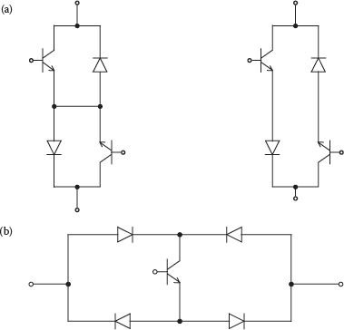
FIGURE 16.3 Conventional implementation of the bi-directional power switch.
The advent of SiC based devices has provided a chance for improvement of these configurations by replacement of diodes with SiC diodes or even prototypes for replacement of the power switches with SiC JFET devices [18]. This approach enabled power density levels in forced air cooled systems to 20 kW/dm3.
Given the success of the matrix converter topology as well as of other converter topologies with bi-directional switches, the RB-IGBT (reverse blocking IGBT) device has been developed recently [19,20]. This new device has advantages in reduction of the voltage drop during the conduction state since series diodes are no longer necessary for reverse blocking capability. An RB-IGBT has the same fundamental structure as a conventional IGBT. Therefore, the trade-off between switching loss and on-state voltage in a RB-IGBT does not differ from that of a conventional IGBT, except for the need for diodes in the conventional bi-directional switch. When reverse biased, the recovery characteristics are the same as for a conventional diode. Products are already available on the market for applications with currents less than 100 A, in the low voltage range [20].
It is worth noting here that the conventional matrix converter equipped with the conventional implementation of the power switch shown in Figure 16.3a allows a reduction of losses in the entire system by 1/3 when compared to the back-to-back converter made of identical IGBT devices [21], or an efficiency change from 94% to 96% [11,21]. The use of RB-IGBT reduces further the system loss by 40% [21]. The power density is also improved by roughly 1/3 from back-to-back converter to the matrix converter [11,21]. Such ballpark numbers worth be remembered even if numerous other loss or efficiency measurements are accurately reported in literature for a multitude of PWM arrangements.
The PWM control of the switches within the matrix converter topology must ensure always a path for the circulation of the load current (usually of inductive nature). On the other hand, two input nodes should never be short-circuited.
The current commutation within bidirectional switches built as shown in Figure 16. 3a has been analyzed in [2,22,23]. Because of the unpredictable time delays at the switch commutation, open- or short-circuit hazards could happen. A multistepped switching procedure is considered in [22,23], which requires independent control of the current flow on the two possible directions of the bidirectional switch.
A possible modeling approach is based on identification of all possible states at current commutation and a local state machine able to secure the multistep procedure. In order to understand this approach, let us herein consider the simplified case of commutation of the load current from an input phase to another (Figure 16.4). Let us assume that we will start from the state with current circulating through leg A, when both switches A12 and A11 have gate signals for turning-on. Conversely, switches B11 and B12 have the gate signals corresponding to the turn-off state. When the current commutation sequence starts and the voltage in the second leg is larger than the grid phase voltage in the first leg, we can use the current direction information and change the gate control for turning-off the switch (A11 or A12) which is anyway off (states 2 and 4 on the second column of Figure 16.5). Next, we can apply the gate signal for turning-on the switch which does not correspond to the current circulation among B11 and B12. Finally, the other switch among B11 and B12 can be turned-on to carry the load current and to turn-off the conducting switch on the first leg.
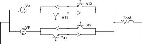
FIGURE 16.4 Sketch for understanding current commutation.
This way, based on grid voltage relationship and load current direction, we can judge all possible state sequences. This yields in the diagram shown in Figure 16.5, which includes all possible cases and codes the migration from a state to another from the input voltage relationship and load current direction. For completeness of information, the case with zero current is also included. Since there are four switches involved (two would have to turn-off and the other two to turn-on), four columns are shown as four intermediary stages of the current commutation process.
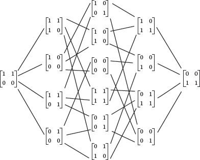
FIGURE 16.5 Diagram of the state transition for proper current commutation.
While Figure 16.5 shows the mathematical modeling of states, different practical solutions for physical implementation have been proposed over time. They all count on either sensing both the output current and input voltage, or at least one among the output current and input voltage. In certain situations, soft turn-on and soft turn-off instances can be achieved due to zero current switching.
16.4 CLAMPING THE REACTIVE ENERGY
Along the conventional IGBT protection circuitry, the matrix converter requires special care in handling the recovery of the reactive energy from the load circuitry since there is no natural free-wheeling path. The common solution is illustrated in Figure 16.6. The grid-side diode rectifier establishes the voltage to clamp to. The capacitor is typically very small and its value depends on nature of load. For instance, a 3 kW Matrix Converter Drive for an Aircraft Application [14,15] at a maximum output current of 30 A and a machine inductance of 1.15 mH requires a capacitor of 2 μF. The capacitor is discharged across an additional resistor or used to power up the other auxiliary power supplies (sensing and measurement, microcontroller, gate drivers, and so on).
An alternative solution for lower power levels consists in the use of varistor devices for clamping voltages across the input and output lines [10].
16.5.1 SINUSOIDAL CARRIER-BASED PWM
Similar to the conventional PWM converter, a modulation function is attributed to each switch and a constant time interval is selected to correspond to the desired carrier frequency. The block diagram is shown in Figure 16.7. The implementation consists of comparing each modulation function with the same carrier triangular signal as in the case of PWM for conventional six-switch converter. Since two input lines should never be short-circuited, the switches on the same row in Figure 16.1 should never conduct at the same moment. Moreover, each output should be connected to an input for the current continuation. This yields:
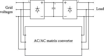
FIGURE 16.6 Clamping circuit for protection.
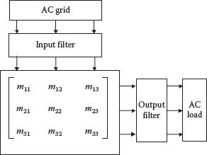
FIGURE 16.7 Introducing the modulation functions.
{m11+m12+m13=1m21+m22+m23=1m31+m32+m33=1
The output–input relationship is given by [24]
[e]=[M] ⋅ [v2] ⇒ [v2]=[M]T ⋅ [e] |
(16.1) |
It has been demonstrated that [M] can be decomposed into two matrices that are basically separating the frequency changer [Mf] and the static VAR compensator [Mϕ] components:
(16.2) |
Moreover,
[Mf(t)]=[C12(0)C12(−2π3)C12(2π3)C12(−2π3)C12(2π3)C12(0)C12(2π3)C12(0)C12(−2π3)] |
(16.3) |
The [Mf] matrix is derived using the d–q to a–b–c transform and considers the power transfer through a fictitious intermediary DC link when the energy transfer through zero-sequence components is not considered. All possible control cases share the same general expression for the direct transfer function [Mf],
[Mf(t)]=[C(ω1)]3×2 ⋅ [P]2×2 ⋅ [C(ω2)]T3×2 |
(16.4) |
Where
[C(ωi)]=[b1(ωi) b2(ωi) b3(ωi)] |
(16.5) |
represents a matrix composed of ortho-normal base vectors of the input or output three-phase systems and [P] represents a matrix of constant weights pij, with the meaning of transfer power.
Let us first consider three different cases:
(A) Choosing
(16.6) |
defines conjugated forms
CA12(x)=23 ⋅ Pf ⋅ cos [(ω1+ω2)t+x] |
(16.7) |
(B) Choosing
(16.8) |
defines nonconjugated forms
CB12(x)=23 ⋅ Pf ⋅ cos [(ω1−ω2)t+x] |
(16.9) |
(C) Considering both the conjugated and nonconjugated forms leads to
(16.10) |
In all of these forms, Pf plays the same the role as the turns ratio of the primary to secondary windings of a magnetic transformer and x=0, 2π3, −2π3.
[The second term ([Mϕ]) is considered when a transfer through the zero sequence is possible to lead to a DC component on the output side. This can be used for instance to compensate the neutral node voltage. The generation of a DC component on the load side is generally not the case of a conventional matrix converter. However, the mathematical modeling is herein included for completeness of information.
[Mϕ(t)]=[C1ϕ(0)C1ϕ(0)C1ϕ(0)C1ϕ(−2π3)C1ϕ(−2π3)C1ϕ(−2π3)C1ϕ(2π3)C1ϕ(2π3)C1ϕ(2π3)] |
(16.11) |
where
(16.12) |
and x=0,2π3,−2π3
Through [Mϕ, the zero sequence voltage V20 can be produced and regulated on output side of the converter which projects an AC voltage at angular frequency ω1 on the input side whose magnitude and phase angle are controllable by Pm and ϕ, respectively.
Any of the above algorithms for [Mf] (the conjugated or nonconjugated forms) produces an output voltage with a limited maximum voltage. A general solution applied in PWM three-phase bridge converters consists of injecting the third harmonic in the modulating waveform. Similar approach is considered for a matrix converter in [25,26] where the output voltage is considered as
This leads to the following mij form of the modulating waveform to produce unity input power factor.
Using these modulation signals improves the maximum available output voltage from 0.500 to 0.866 of the peak of the input voltage (Figure 16.8). As will be shown later on, similar results can be achieved with Space Vector Modulation [27].
The generation of the gate control pulses is achieved with a comparison between these reference signals and a triangular carrier waveform. The solution proposed in [25] considers a single-ended carrier (Figure 16.9). It can also be improved for reduction of the switching processes with a double-sided symmetrical pulse generation. Either case, the sequence is selected so that the input voltage with the largest instantaneous value corresponds to the state placed in the middle (like phase “2” in the figure).
16.5.2 SPACE VECTOR MODULATION CONSIDERING ALL POSSIBLE SWITCHING VECTORS
Almost all the previously reported Space Vector PWM algorithms are based on the stationary vectors and a clear and convincing, comparative analysis of the use of all the switching combinations has not been reported yet. Ref. [3] develops the mathematical model and the appropriate control algorithm for the use of all the available switching combinations including the calculus of the time portions, simulation results, and the steps for the implementation of an algorithm based on all the switching vectors.
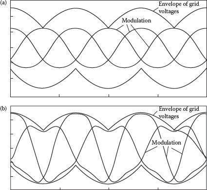
FIGURE 16.8 Reference modulation waveforms for (a) conventional, (b) extended voltage range.
Intuitively, the generation of the desired space vector by averaging in between two adjacent vectors closer to each other than in the case of a conventional six-switch inverter (that is 60°) would improve the quality of the output voltage waveform. This principle was used successfully at multilevel power inverters. The difference here is the rotation of one of the vectors that suggests the use of a high enough switching frequency. Moreover, there is no obvious advantage in the input (grid side) currents as the PWM cannot easily be optimized for the input when both stationary and rotating vectors are used.
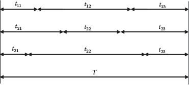
FIGURE 16.9 Example of state sequence.
Applying the voltage space vector to a three-phase R–L load leads to a phase shift in between the voltage and current space vectors in the complex plane of the load reference frame. The input currents can be derived by reflecting these output currents through the matrix converter. They can be determined from the output current space vector by analyzing the system of all switching vectors in the grid source reference frame. The input current space vectors that correspond to the main voltage switching vectors are fixed while those corresponding to the “stationary” vectors are rotating at a relative speed determined by the mains and output frequencies. It can be inferred that the phase angle in between the voltage and current space vectors at the fundamental frequency is preserved.
16.5.2.1 Selection of the Closest Rotating and Stationary Vectors
The desired vector position is defined with polar coordinates (V,a). The angular resolution is ensured similarly at both small and large magnitudes of desired vector. The selection of the closest Rotating and Stationary vectors can be simplified in a digital implementation by defining all the angular coordinates as binary words with the three most significant bits set up for sector number, as a divide-by-six counter.
On the load reference frame, the rotating vector Vm1 is superimposed on the real axis when the vin1 voltage is maximum. In order to avoid the dependence of the angular coordinate of Vm1 on the supply frequency variations, synchronization is achieved by a PLL circuit from the vin2,3 input grid voltage. The absolute value of angular coordinate of the rotating vector Vm1 can be read from a counter placed in the loop of the PLL circuit. A fast selection of the line voltage that defines the Stationary vector magnitude is obtained with the three most significant bits of this counter.
Finally, the sequence of states can be selected as
Zero vector → stationary vector → rotating vector → zero vector
and this is applied on each sampling interval. Analogous to the harmonic reference generation from Section 5.7.1, a double-sided PWM can be generated.
16.5.2.2 Definition of Time Intervals
Any instantaneous position of the desired load-side voltage vector is always placed in between a rotating and a stationary vector. A generalized sector bounded by a rotating vector (denoted with index “m”) and a stationary vector (denoted with index “s”) is dynamically defined analogous with [6,7] (Figure 16.10). This simplifies the calculation of the time constants. Definition of the time portions allocated to the switching vectors yields from the averaging relationship:
(16.15) |
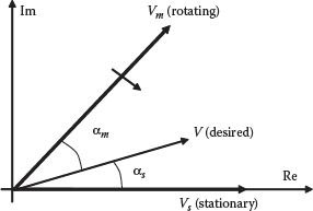
FIGURE 16.10 Calculation of time intervals allocated to each state.
where tm + ts + t0 = T
The calculation is performed with the projection of both desired and switching vectors on Real and Imaginary axis, one of the stationary switching vectors having the same direction as the hypothetical Real axis of the load reference frame (Figure 16.2). This yields:
Re:T⋅V⋅cosα=[1TT∫0(ReVs→)dt] ⋅ ts+[1TT∫0(ReVm→)dt] ⋅ tmIm:T⋅V⋅sinα=[1T T∫0(ImVs→)dt] ⋅ ts+[1TT∫0(ImVm→)dt]⋅tm |
(16.16) |
Solving the system for the situation of a high pulse rate—when the effects of the rotation of the reference system can be overlooked—and taking into consideration the dependency of the secondary vector magnitude with αs and αm yields the solution:
tm=VVm T⋅sinαssin(αs+αm)=V√2⋅E ⋅T⋅sinαssin(αs+αm)ts=VVs⋅T⋅sinαmsin(αs+αm)=V√2⋅E⋅T⋅sinαmsin(αs+αm)⋅cosπ3cos(π6−(αs+αm)) |
(16.17) |
These time intervals are the same for both possible successions of the rotating and stationary vectors. The portions of time allocated to the null-states over the sampling period can be considered equal with each other and are calculated with
t01=t02= 12⋅T ⋅ [1−VVi⋅cos(π6−αs)cos(π6−αs−αm)]=12⋅ T ⋅ [1−V√2⋅E ⋅ cos(π6−αs)cos(π6−αs−αm)] |
(16.18) |
The maximum attainable modulation index is defined as Vrms/Vin and it is calculated to be 0.866. This value equals the maximum achievable with the conventional back-to-back converter as well as with the improved carrier-based PWM for matrix converter [2].
An example of waveforms defining operation of the matrix converter with a PWM algorithm derived from vectorial analysis of the power stage with consideration of both the stationary and rotating vectors is shown in Figure 16.11.
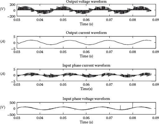
FIGURE 16.11 Waveforms at the matrix converter terminals for N = 72, f1 = 30 Hz, T = 0.001388 s, m = 0.7, load composed of R = 5 ohm, L = 50 mH.
16.5.3 SPACE VECTOR MODULATION CONSIDERING STATIONARY VECTORS ONLY
Since the previous PWM algorithm is complex, very dependent on synchronization with the phase of the input grid voltages, and without proven major benefits, a Space Vector Modulation based on only the stationary vectors is generally considered [28]. All switching combinations are shown in Table 16.1 along with the values for the generated output voltage. The vectorial representation is shown in Figure 16.12 and we can see that each vectorial position for the output voltage space vector can be achieved with multiple combinations of switches.
The PWM algorithm is very intuitive as it can be seen as a superposition of a rectifier-inverter back-to-back system without an intermediary DC link.
The same Equation 5.30 as in the case of a three-phase inverter can be used here:
{ta=3Vs2Vrec⋅Ts⋅(cosα−1√3sin α)=√3⋅VsVrecTs⋅sin[π3−α]tb=√3⋅VsVrec⋅Ts⋅sinαt0=TS−ta−tb |
(16.19) |
where the DC voltage has been replaced with a variable signal Vrec corresponding to the instantaneous average of the three-phase PWM rectified voltage.
A simplified approach considers the “rectifier” as a three-phase diode rectifier, operating as a selector of the highest line-to-line voltage in the input, voltage that is applied to the “inverter” side [29,30] (consider Figure 1.2 without the intermediary DC link module). The “rectifier” side is therefore not modulated, with pairs of switches being commutated at each 60°. The DC link voltage Vrec follows the line-to-line voltage, and so does its moving average, calculated at the sampling frequency. Compensation of this fluctuation can be achieved with a simple feed-forward use of the rectified voltage into Equation 16.19 (Figure 16.13). Sample results are shown in Figure 16.14. The 120° conduction intervals for each input current can be seen.
If this solution had its obvious merits when implemented with a real rectifier-inverter structure without a DC link capacitor, it does not make use of all resources when implemented within a 9-switch matrix converter.
If the input phase currents are required to be controlled (displacement power factor), a PWM operation of the fictitious “rectifier” should be considered. The fictitious “rectifier” operates now as a Current Source Converter with two switches conducting the DC-side current at any moment. The intermediary DC link voltage and current are now shown in Figure 16.15. The moving average calculated at each interval equal to the PWM sampling interval is also shown in the figure, and it looks like a reversed rectified voltage [11] (Figure 16.16).
The calculation of the time intervals allocated to each state can be expressed in dependence to the phase of the input voltage and current using the information about the averaged fictitious DC link voltage as depicted from Figure 16.16. In the most general case, when the phase of the input current is required to be controllable, these equations yield:
TABLE 16.1
Switching Sequences and Voltages, Considering Input Nodes as R,S,T and Output Nodes as a,b,c
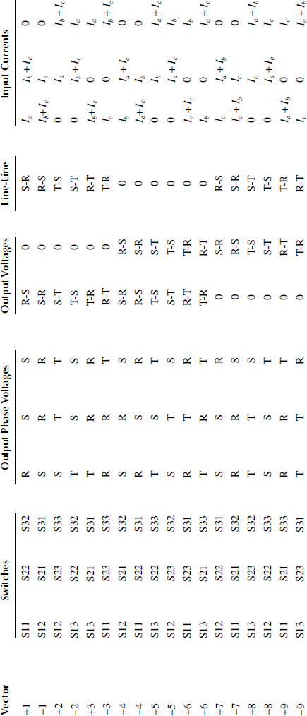
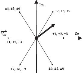
FIGURE 16.12 Possible switching vectors derived from stationary vectors shown in Table 16.1.
{ta=2√3⋅VsV1.cos(Φ)⋅(cos[Φi−π6].Ts.sin[π3−α]tb=2√3⋅VsV1.cos(Φ)⋅(cos[Φi−π6].Ts.sinαt0=TS−ta−tb |
(16.20) |
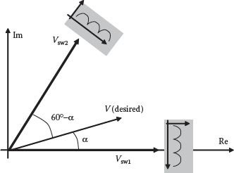
FIGURE 16.13 Calculation of time intervals allocated to each state for the “inverter” operation when considering the DC link fluctuations in the case of fictitious rectifier-inverter modeling, without any modulation on the grid-side.
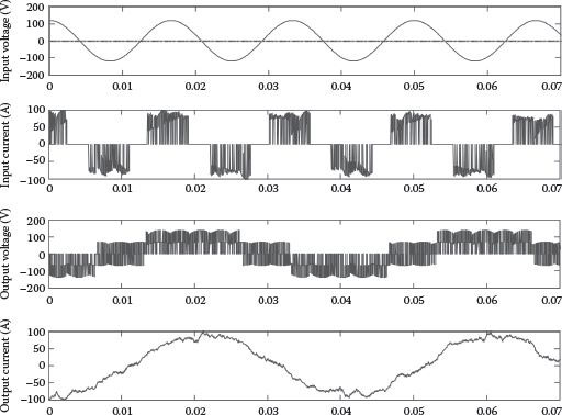
FIGURE 16.14 Characteristic waveforms for operation without modulation of the fictitious rectifier. Operation with modulation index m = 0.7, output frequency fo = 12.5 Hz, switching frequency 5.4 kHz, with grid at 120 V and 60 Hz, and R–L load with L = 1 mH, R = 1 Ohm.
where ϕl represents the instantaneous angular coordinate of the input current in the complex plane with input-side reference frame, bounded within a 60° sector in between adjacent current vectors; and Φ= ϕu − ϕi represents the voltage-current phase shift for the input. For the operation with unity power factor, cos Φ = 1.
The theory presented so far does not guarantee the control of the displacement factor in the input. Since there is no rule for the selection of the state corresponding to a desired active vector, we can use this degree of freedom for selecting the state which allows a control of the displacement factor. The idea is to generate each switching state with two vectors, or to use four active states over a sampling interval. For instance, the Vsw1 position can be achieved with any of the states ±1, ±2, ±3, and the Vsw2 position can be achieved with any of the states ±7, ±8, ±9 (Figure 16.12). For displacement factor control, Figure 16.17 shows the input current vectors corresponding to each state.
The same principle for generation of the desired vector position is used as in the case of a Current Source Converter. The free-wheeling states (zero vector) are reserved now for the “inverter” stage, and the PWM for the current vector is reduced at splitting each of the states ta and tb from the “inverter” operation into two states for modulation of the input current. It yields:
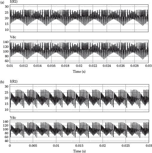
FIGURE 16.15 Generic DC link voltage and current for unity power factor (a) or 45° phase shift (b) on the grid side, and without any capacitor in the DC link (fsw = 10 kHz).
{ta1=ta⋅sin[π3−φi]cos(φi−π6)ta2=ta⋅sin[φi]cos(φi−π6) {tb1=tb⋅sin[π3−φi]cos(φi−π6)tb2=ta⋅sin[φi]cos(φi−π6) |
(16.21) |
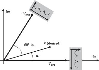
FIGURE 16.16 Calculation of time intervals allocated to each state for the “inverter” operation when considering the DC link fluctuations produced by the PWM operation of the rectifier side within the fictitious rectifier-inverter modeling.
As mentioned, ϕl represents the instantaneous angular coordinate of the input current in the complex plane with input-side reference frame, measured from an active current vector into a 60° sector. This is equivalent with
{ta1=2√3⋅VsV1⋅cos (Φ)⋅Ts⋅sin [π3−α]⋅sin [π3−φi]ta2=2√3⋅VsV1⋅cos (Φ)⋅Ts⋅sin [π3−α]⋅sin [φi]{tb1=2√3⋅VsV1⋅cos (Φ)⋅Ts⋅sin α⋅sin [π3−φi]tb2=2√3⋅VsV1⋅cos (Φ)⋅Ts⋅sin α⋅sin [φi] |
(16.22) |
This helps producing a set of sinusoidal input currents with any desired phase shift. As the desired input current vector rotates within this complex plane representation, the most suitable states are selected for PWM generation. Starting from this principle, multiple PWM switching sequences are yet possible and they were reported in literature. The most known method uses four active vector states over each sampling period (Figure 16.18) [1], and this is considered herein for the waveform examples.
Results for this method are shown in the following figures:
• High modulation index m = 0.7, output frequency fo = 12.5 Hz (Figure 16.19);
• Low modulation index m = 0.15, output frequency fo = 12.5 Hz (Figure 16.20);
• High modulation index m = 0.7, output frequency fo = 52.0 Hz (Figure 16.21);
• Low modulation index m = 0.15, output frequency fo = 52.0 Hz (Figure 16.22).
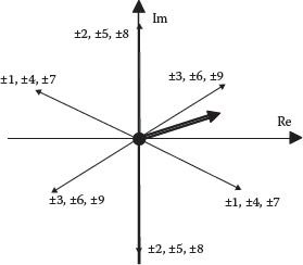
FIGURE 16.17 Vectorial positions for the input current.
The use of stationary vectors means that two input nodes (phases) are connected to the converter at a given moment, and also that two output nodes are connected to the same input node, while the third output node (phase) is connected to another input node (phase).
This form of the Space Vector Modulation can be found similar to the results from [9,11] for the Indirect Matrix Converter, also presented later on in this Chapter.
16.5.4 INDIRECT MATRIX CONVERTER (SPARSE CONVERTER)
As suggested by the matrix form equations described in Section 16.5.1, the operation of the conventional matrix converter can be understood as a sequence of a rectifier operation followed with an inverter without any intermediary DC link capacitor bank. This means the three-phase AC input voltages are rectified into a 6-pulse waveform before being applied to a conventional 6-switch three-phase inverter (Figure 16.23).
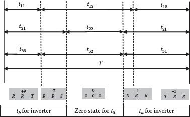
FIGURE 16.18 Example of pulse generation for Direct Space Vector Modulation with four active states.
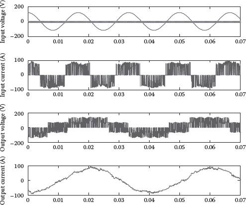
FIGURE 16.19 Operation waveforms for high modulation index m = 0.70, output frequency f0 = 12.5 Hz (40 ms), switching frequency 5.4 kHz, with grid at 120 V and 60 Hz, and R–L load with L = 1 mH, R = 1 Ohm.
This PWM principle is also called Indirect PWM and it can also allow us to develop a new converter structure that actually does operate with the waveforms considered fictitiously for the description above. This is not identical with a back-to-back converter since it requires bi-directional switches for the implementation of the front-end converter. It comes from the requirement for a full recovery of the reactive energy and a four-quadrant operation of the converter. The circuit is shown in Figure 16.24 and it is referred to as Indirect Matrix Converter (Sparse Converter).
16.5.5 IMPLEMENTATION OF PWM CONTROL
There are a multitude of possibilities for implementation of any of the methods suggested above. The most important aspect relates to the necessity of a dedicated “glue logic” circuitry after the conventional counter/timer circuits. This logic circuit is used for selection of the proper switching sequence for the nine bidirectional switches as well as for implementing the logic for the current commutation.
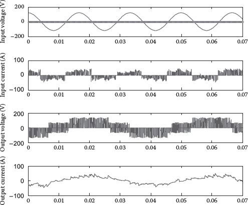
FIGURE 16.20 Operation waveforms for low modulation index m = 0.15, output frequency f0 = 12.5 Hz (40 ms), switching frequency 5.4 kHz, with grid at 120 V and 60 Hz, and R–L load with L = 1 mH, R = 1 Ohm.
A possible architecture is herein described and it is useable for either direct or indirect PWM. The microcontroller software is supposed to manage the characteristics of the desired output waveform depending on application requirements. A PLL type module is required to acquire synchronization with the grid and to sense the phase of the grid power system. The PWM software routine has as inputs:
• Required output phase and magnitude (modulation index);
• Grid instantaneous phase information.
This information is coded in two operation indices: K = number corresponding to the sector where the desired output vector belongs to in the complex plane of output reference frame; J = number corresponding to the sector where the input current vector belong to in the complex plane of input reference frame and which is determined by the external PLL information.
The software routine calculates the time intervals allocated to each state. This may be achieved with SVM type of formula, including compensation for fluctuation within the fictitious DC link voltage. The numerical values for the time intervals can be arranged as shown in Figure 16.25. A single counter with multiple compare features, or 5 separate counters can be used. Counter overflow signals are used along with two operation indices to generate the actual gate control. A memory look-up table, an IF/THEN software sequence, or a logic circuit can be used to synthesize the gate control of the 9 switches from these 7 signals (5 counter overflow and 2 operation indices).
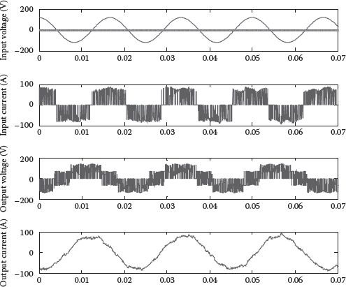
FIGURE 16.21 Operation waveforms for high modulation index m = 0.70, output frequency f0 = 52.0 Hz (22 ms), switching frequency at 5.4 kHz, with grid at 120 V and 60 Hz, and R–L load with L = 1 mH, R = 1 Ohm.
Designing a PWM algorithm means averaging in between these available states in order to emulate a rotating vector in the load reference frame. Various methods are hence available (Figure 16.26).
Matrix converters are a very attractive subject for academic research and development as it offers work with advanced concepts of PWM and filtering, or voltage and current source operation. The success of the conventional matrix converters is limited when trying to replace the conventional back-to-back converter solutions. Alternatively, other direct converter topologies seem more attractive for future exploration as they overcome issues with both the conventional matrix converter and the back-to-back converter. Such issues are:
• Limited output voltage (m = 0.866);
• Complex commutation process;
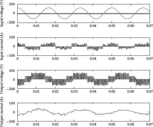
FIGURE 16.22 Operation waveforms for low modulation index m = 0.15, output frequency f0 = 52.0 Hz (22 ms), switching frequency 5.4 kHz, with grid at 120 V and 60 Hz, and R–L load with L = 1 mH, R = 1 Ohm.
• Irregular topology for packaging and volume production;
• Restricted reactive power compensation capability;
• Limited operation at unbalanced input voltages.
These are overcome by solutions further described in Chapter 18.
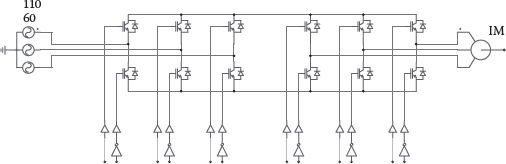
FIGURE 16.23 Conceptual back-to-back converter used for definition of a PWM algorithm.
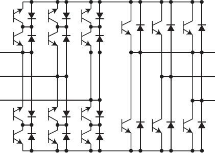
FIGURE 16.24 Indirect Matrix Converter.
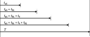
FIGURE 16.25 Time constants and counter arrangement.
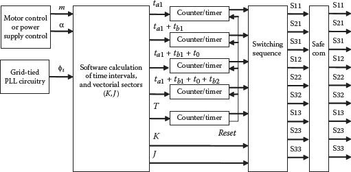
FIGURE 16.26 Digital architecture for implementation of the PWM algorithms.
1. Borojevic, D. 1991. Space vector modulation in matrix converters. VPEC Virginia Power Electron. Center 5(1,2).
2. Huber, L. and Borojevic, D. 1991. Space vector modulation with unity input power factor for forced commutated cycloconverters. Proceedings of PESC, pp.1032–1041.
3. Neacsu, D.O. 1995. Theory and design of a space vector modulator for AC/AC matrix converter. European Trans. Electr. Power Eng. 4, 285–292.
4. Neft, C.L. and Shauder, C.D. 1988. Theory and design of a 30-HP matrix converter. Proceedings of IEEE IAS’88, pp. 248–253.
5. Nielsen, P., Blaabjerg, F., and Pedersen, J.K. 1996. SVM matrix converter with minimized number of switchings and a feed forward compensation of input voltage unbalance. PEDES’96, New Delhi, January 8–11.
6. Halasz, S., Schmidt, I., and Molnar, T. 1995. Matrix converters for induction motor drive. EPE’95, Sevilla, Spain.
7. Bernet, S., Matsuo, T., and Lipo, T.A. 1996. A matrix converter using reverse blocking NPT-IGBT’s and optimized pulse patterns. IEEE PESC’96, Baveno, Italy, vol. 1, pp. 107–113.
8. Anon. 2008. AC7 matrix converter—Application Note, Document AN.AC7.01. Yaskawa Electric America, April.
9. Friedli, T. and Kolar, J.W. 2012. Milestones in matrix converter research. IEEJ J. Industry Appl. 1(1), 2–14.
10. Matteini, M. 2001. Control techniques for matrix converter adjustable speed drives. University of Bologna, Italy, PhD Thesis.
11. Kolar, J.W. and Friedli, T. 2010. Comprehensive evaluation of three-phase AC-AC PWM converter systems. Tutorial at IEEE IECON.
12. Yamamoto, E., Hara. H., Uchino, T., Kume, T.J., Kang, J.K., and Krug, H.P. 2007. Development of matrix converter for industrial applications. Yaskawa White Paper.
13. Lai, R., Pei, Y., Wang, F., Burgos, R., Boroyevich, D., Lipo, T.A., Immanuel, V., and Karimi, K. 2007. A systematic evaluation of AC-fed converter topologies for light weight motor drive applications using SiC semiconductor devices. Proceedings IEEE Int’l Electric Machines and Drives IEMDC, vol. 2, pp. 1300–1305.
14. Wheeler, P. and Clare, J. 2005. Matrix converter technology. Tutorial IEEE IECON.
15. Wheeler, P., Rodriguez, J., Clare, J.C., Empringham, L., and Weinstein, A. 2002. Matrix converters: A technology review. IEEE Trans. Industrial Electron. 49(2), 276–288.
16. Anon. 2010. DIM400PBM17-A000 IGBT bi-directional switch module. DS5524-3 November 2010 (LN27710).
17. Anon. 2001. Datasheet of FM35R12KE3. Infineon Technologies, 2001-08-16.
18. Schulz, M., De Lillo, L., Empringham, L., and Wheeler, P. 2011. Pushing power density limits using SiC-Jfet-based matrix converter. In: PCIM Europe Conference, VDE VERLAG GMBH, Berlin, Offenbach, vol. 1, 17–19 May 2011, pp. 464–470.
19. Motto, E.R., Donlon, J.F., Tabata, M., Takahashi, M., Yu, Y., and Majumdar, G. 2004. Application characteristics of an experimental RB-IGBT. IEEE/IAS Ann. Meeting Conf. Rec., vol. 3, pp. 1540–1544, October.
20. Takei, M., Naito, T., and Ueno, K. 2010. The Reverse Blocking IGBT for Matrix Converter with Ultra-Thin Wafer Technology, Fuji.
21. Itoh, J., Odaka, A., and Sato, I. 2004. High efficiency power conversion using a matrix converter. Fuji Electr. Rev. 50(3), 94–98.
22. Burany, N. 1989. Safe control of four-quadrant switches. IEEE IAS Conference Record 1989, part I, pp. 1190–1194.
23. Oyama, J., Higuchi, T., Yamada, E., Koga, Y., and Lipo, T. 1989. New control strategy for matrix converter. IEEE PESC’89 Conference Record, pp. 360–367.
24. Ooi, B.T. and Kazerani, M. 1994. Application of dyadic matrix converter theory in conceptual design of dual field vector and displacement factor controls. IAS Annual Meeting 1994, pp. 903–910.
25. Venturini, M. and Alesina, A. 1980. The generalized transformer: A new bidirectional sinusoidal waveform frequency converter with continuously adjustable input power factor. IEEE Power Electronics Specialists Conference Record, pp. 242–252.
26. Watthanasarn, C., Zhang, L., and Liang, D.T.W. 1996. Analysis and DSP-based implementation of modulation algorithms for AC-AC matrix converters. IEEE-PESC 1996, pp. 1053–1058.
27. Klumpner, C., Blaabjerg, F., Boldea, I., and Nielsen, P. 2006. New modulation method for matrix converters. IEEE Trans. Industry Appl. 42(3), 797–803.
28. Huber, L. and Borojevic, D. 1995. Space vector modulated three-phase to three-phase matrix converter with input power factor correction. IEEE Trans. Industry Appl. 31(6), 1234–1246.
29. Ziogas, P.D., Kang, Y., and Stefanovic, V.R. 1986. Rectifier-inverter frequency changers with suppressed DC link components. IEEE Trans. Industry Appl. IA-22(6), 1027–1036.
30. Kim, S., Sul, S.K., and Lipo, T.A. 2000. AC/AC power conversion based on matrix converter topology with unidirectional switches. IEEE Trans. Industry Appl. 36(1), 139–145.