
General-purpose I/O is a topic near to the hearts of Raspberry Pi owners because this is the interface to the outside world. The Pi is flexibly designed to allow I/O pins to be reconfigured under software control. For example, GPIO 14 can be an input, an output, or operate as a serial port TX data line.
One of the challenges related to the Pi’s GPIO interface is that it uses a weak CMOS 3.3 V interface. The GPIO pins are also susceptible to ESD (electrostatic discharge) damage and are weak drivers (2 to 16 mA). Finally, the limited GPIO power must be budgeted from the total spare current capacity (50 mA on the original Pi Model B). Using adapter boards overcomes these problems but can add considerably to the cost. Consequently this provides a fertile area for coming up with cheap and effective roll-your-own solutions.
Pins and Designations
Odd-Numbered GPIO Pins for the Modern Raspberry Pi
Pin | GPIO | Name | Description |
|---|---|---|---|
P1-01 | +3.3 V Power supply, from regulator | ||
P1-03 | GPIO-2 | I2C SDA1(with 1.8 kΩ pull-up resistor) | |
P1-05 | GPIO-3 | I2C SCL1 (with 1.8 kΩ pull-up resistor) | |
P1-07 | GPIO-4 | GPIO_GCLK | General-purpose clock output or 1-Wire |
P1-09 | Ground | ||
P1-11 | GPIO-17 | GPIO_GEN0 | |
P1-13 | GPIO-27 | GPIO_GEN2 | |
P1-15 | GPIO-22 | GPIO_GEN3 | |
P1-17 | +3.3 V Power supply, from regulator | ||
P1-19 | GPIO-10 | SPI_MOSI | |
P1-21 | GPIO-9 | SPI_MISO | |
P1-23 | GPIO-11 | SPI_CLK | |
P1-25 | Ground | ||
P1-27 | ID_SD | I2C ID EEPROM Data | |
P1-29 | GPIO-5 | ||
P1-31 | GPIO-6 | ||
P1-33 | GPIO-13 | ||
P1-35 | GPIO-19 | ||
P1-37 | GPIO-26 | ||
P1-39 | Ground |
Even-Numbered GPIO Pins for the Modern Raspberry Pi
Pin | GPIO | Name | Description |
|---|---|---|---|
P1-02 | +5 V Power supply | ||
P1-04 | +5 V Power supply | ||
P1-06 | Ground | ||
P1-08 | GPIO-14 | TXD0 | UART transmit |
P1-10 | GPIO-15 | RXD0 | UART receive |
P1-12 | GPIO-18 | GPIO_GEN1 | |
P1-14 | Ground | ||
P1-16 | GPIO-23 | GPIO_GEN4 | |
P1-18 | GPIO-24 | GPIO-GEN5 | |
P1-20 | Ground | ||
P1-22 | GPIO-25 | GPIO-GEN6 | |
P1-24 | GPIO-8 | SPI_CE0_N | |
P1-26 | GPIO-7 | SPI_CE1_N | |
P1-28 | ID_SC | I2C ID EEPROM Clock | |
P1-30 | Ground | ||
P1-32 | GPIO-12 | ||
P1-34 | Ground | ||
P1-36 | GPIO-16 | ||
P1-38 | GPIO-20 | ||
P1-40 | GPIO-21 |
GPIO Cross Reference
GPIO Cross Reference
GPIO | Pin | GPIO | Pin | GPIO | Pin | GPIO | Pin |
|---|---|---|---|---|---|---|---|
GPIO-2 | P1-03 | GPIO-9 | P1-21 | GPIO-16 | P1-36 | GPIO-23 | P1-16 |
GPIO-3 | P1-05 | GPIO-10 | P1-19 | GPIO-17 | P1-11 | GPIO-24 | P1-18 |
GPIO-4 | P1-07 | GPIO-11 | P1-23 | GPIO-18 | P1-12 | GPIO-25 | P1-22 |
GPIO-5 | P1-29 | GPIO-12 | P1-32 | GPIO-19 | P1-35 | GPIO-26 | P1-37 |
GPIO-6 | P1-31 | GPIO-13 | P1-33 | GPIO-20 | P1-38 | GPIO-27 | P1-13 |
GPIO-7 | P1-26 | GPIO-14 | P1-08 | GPIO-21 | P1-40 | ||
GPIO-8 | P1-24 | GPIO-15 | P1-10 | GPIO-22 | P1-15 |
|
Configuration After Reset
Upon reset, most GPIO pins are configured as general-purpose inputs with some exceptions. However, as Raspbian Linux changes and new Pi models get introduced, there is probably no boot GPIO state that is safe to assume. If you use a GPIO, then it should be configured before use.
Pull-Up Resistors
As noted earlier, GPIO 2 and 3 (I2C pins) have an external resistor tied to the +3.3 V rail to meet I2C requirements. The remaining GPIO pins are pulled high or low by an internal 50 kΩ resistor in the SoC. The internal pull-up resistor is weak and effective at only giving an unconnected GPIO input a defined state. A CMOS (complementary metal oxide semiconductor) input should not be allowed to float midway between its logic high and low. When pull-up resistance is needed for an external circuit, it is probably best to provide the external pull-up resistor, rather than relying on the weak internal one.
Configuring Pull-Up Resistors
The Raspberry Pi GPPUP Register
Bits | Field | Description | Type | Reset |
|---|---|---|---|---|
31-2 | - | Unused, GPIO pin pull-up/down | R | 0 |
1-0 | PUD | 00 Off—disable pull-up/down 01 Pull-down enable 10 Pull-up enable 11 Reserved | R/W | 0 |
The GPPUDCLK0 Register Layout
Bits | Field | Description | Type | Reset | |
|---|---|---|---|---|---|
31-0 | PUDCLKn | n = 0..31 | R/W | 0 | |
0 | No effect | ||||
1 | Assert clock | ||||
The GPPUDCLK1 Register Layout
Bits | Field | Description | Type | Reset | |
|---|---|---|---|---|---|
31-22 | - | Reserved | R | 0 | |
21-0 | PUDCLKn | n = 32..53 | R/W | 0 | |
0 | No effect | ||||
1 | Assert clock | ||||
- 1.
Write the pull-up configuration desired in the rightmost 2 bits of the 32-bit GPPUP register. The configuration choices are as follows:
00: Disable pull-up control.
01: Enable pull-down control.
10: Enable pull-up control.
- 2.
Wait 150 cycles to allow the preceding write to be registered.
- 3.
Write a 1-bit to every GPIO position, in the group of 32 GPIO pins being configured.
GPIOs 0–31 are configured by register GPPUDCLK0.
- 4.
Wait another 150 cycles to allow step 3 to register.
- 5.
Write 00 to GPPUP to remove the control signal.
- 6.
Wait another 150 cycles to allow step 5 to register.
- 7.
Finally, write to GPPUDCLK0/1 to remove the clock.
The Broadcom procedure may seem confusing because of the word clock. Writing to GPPUP and GPPUDCLK0/1 registers by using the preceding procedure is designed to provide a pulse to the internal pull-up resistor flip-flops (their data clock input). First a state is established in step 1, and then the configured 1 bits are clocked high in step 3 (for selected GPIO pins). Step 5 establishes a zero state, which is then sent to the flip-flop clock inputs in step 7.
The documentation also states that the current settings for the pull-up drivers cannot be read (there is no register access available to read these flip-flops). This makes sense when you consider that the state is held by these internal flip-flops that were changed by the procedure. Fortunately, when configuring the state of a particular GPIO pin, you change only the pins that you select by the GPPUDCLK0/1 register. The others remain unchanged. Chapter 16 will demonstrate how to change the pull-up resistors in a C program.
Drive Strength
How much drive can a GPIO pin provide in terms of current? The design of the SoC (system on chip) is such that each GPIO pin can safely sink or source up to 16 mA without harm. The drive strength is software configurable from 2 to 16 mA.
GPIO Pads Control
Bits | Field | Description | I/O | Reset | |
|---|---|---|---|---|---|
31:24 | PASSWRD | 0x5A | Must be 0x5A when writing | W | 0x00 |
23:05 | Reserved | 0x00 | Write as zero, read as don’t care | R/W | |
04:04 | SLEW | Slew rate | |||
0 | Slew rate limited | R/W | 1 | ||
1 | Slew rate not limited | ||||
03:03 | HYST | Enable input hysterisis | |||
0 | Disabled | R/W | 1 | ||
1 | Enabled | ||||
02:00 | DRIVE | Drive strength | R/W | 3 | |
0 | 2 mA | ||||
1 | 4 mA | ||||
2 | 6 mA | ||||
3 | 8 mA (default except 28 to 45) | ||||
4 | 10 mA | ||||
5 | 12 mA | ||||
6 | 14 mA | ||||
7 | 16 mA (GPIO 28 to 45) | ||||
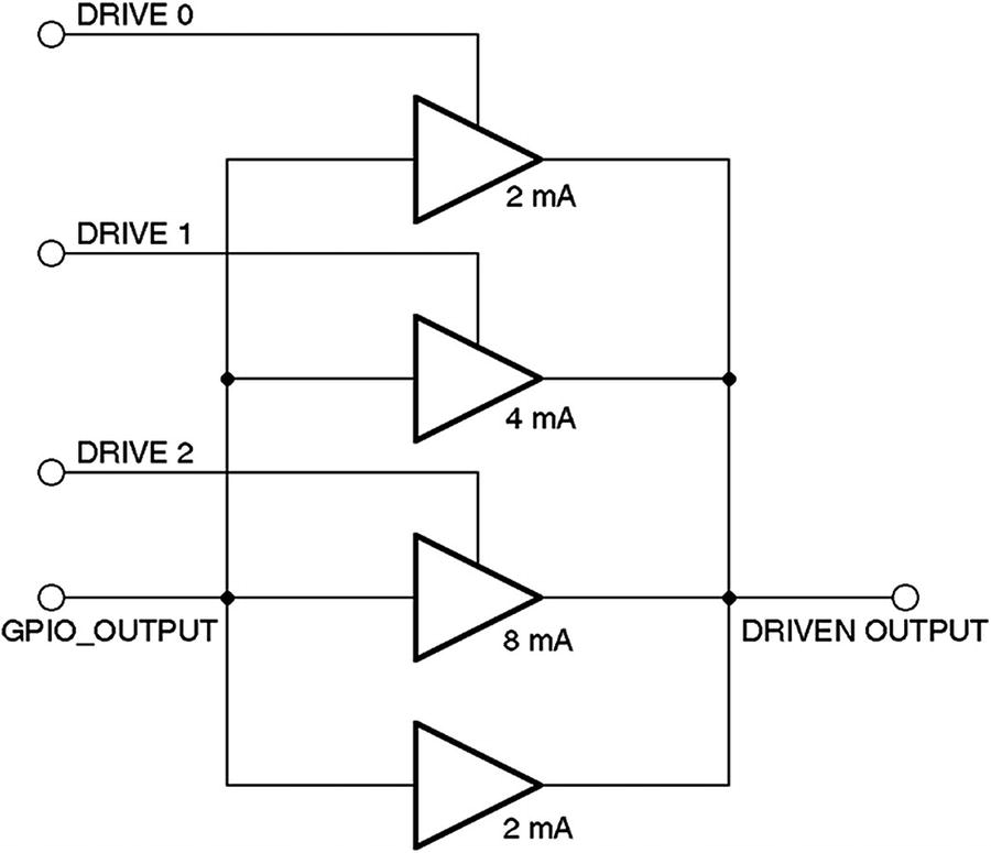
Drive-strength control
With Drive 0 set to a 1, the top amplifier is enabled, adding another 2 mA of drive, for a total of 4 mA. Enabling Drive 1 adds a further 4 mA of drive, totaling 8 mA. Enabling Drive 2 brings the total drive capability to 16 mA.
It should be mentioned that these drive capabilities are not current limiters. What they do is apply more or less amplifier drive. If the GPIO output is wired up to a light load like a CMOS chip or MOSFET transistor where little current is drawn, then the minimum drive of 2 mA suffices. When the GPIO output is loaded with a higher current load, the single 2 mA buffer may not be enough to keep the logic level within spec. By applying more drive, the output voltage levels are coerced into the correct operating range.
Logic Levels
Parameter | Volts | Description |
|---|---|---|
V IL | ≤ 0.8 | Voltage, input low |
V IH | ≥ 1.3 | Voltage, input high |
The voltage levels between VIL and VIH are considered to be ambiguous or undefined for logic values 0 and 1 respectively and must be avoided. When driving current loads like an LED, this is less important.
Input Pins
A GPIO input pin should experience voltages only between 0 and the 3.3 V maximum. Exercise caution when interfacing to other circuits that use higher voltages like TTL logic, where 5 V is used. The SoC is not tolerant of overvoltages and can be damaged.
While there exist protection diodes on chips to prevent negative input swings and overvoltage, these are weak and intended only to bleed away static charges. Broadcom does not document the current capacity of these protective diodes.
Output Pins
As an output GPIO pin, the user bears full responsibility for current limiting. There is no current limiting provided. When the output pin is in the high state, as a voltage source, it tries to supply 3.3 V (within the limits of the transistor and the supplying voltage regulator).
If this output is shorted to ground, then as much current as can be supplied will flow. This could lead to permanent damage.
The outputs also work to the voltage specifications listed earlier. But the attached load can skew the operating voltage range. An output pin can source or sink current. The amount of current required and the amount of output drive configured alters the operating voltage profile. As long as you keep within the current limits for the configured drive capability, the voltage specifications should be met by your Pi.
Sourcing Current
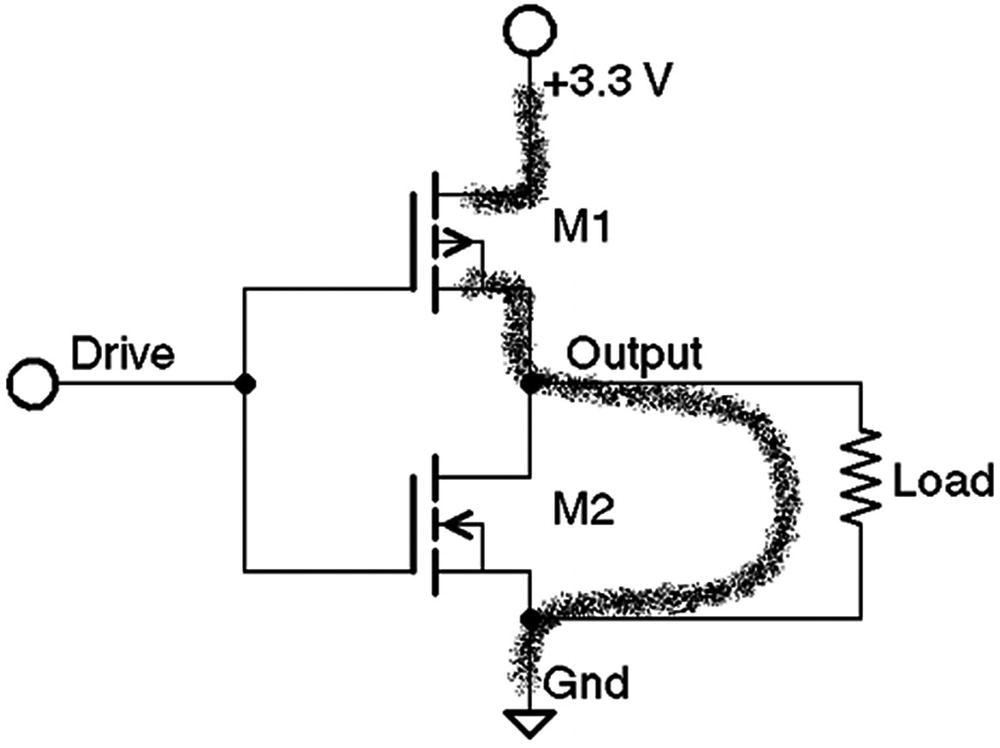
The GPIO sourcing current through the load from transistor M1
Sinking Current
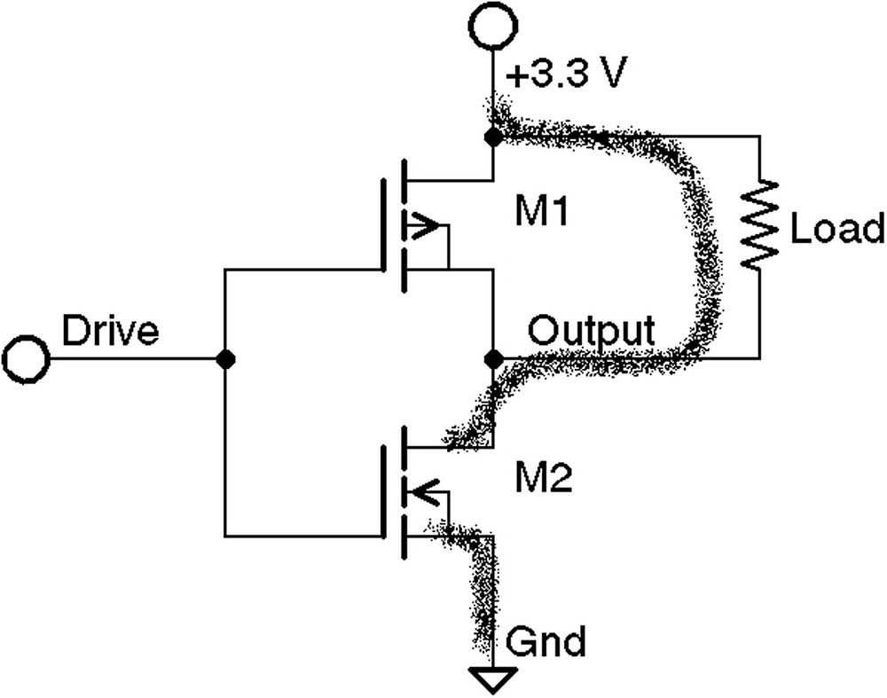
GPIO sinking current from the load through M2
Driving LEDs

Raspberry Pi GPIO driving two LEDs through a limiting resistor. Active high configuration at (A) left. Active low configuration at (B) right.
The MOSFETs used in the GPIO output driver, are complementary. Notice how the arrow in the symbol for M1 differs from M2. These transistors act as switches. The drive signal is inverted from the GPIO output bit written. The drive signal to the gate of M1 and M2 is low when a 1-bit is written to the output. A low turns M1 on while simultaneously turning off M2. In this manner, only the upper or lower transistor is on for a given drive signal.
When the GPIO is written with a 1-bit, LED1 is lit because the GPIO transistor M1 is sourcing current through LED1 (review Figure 11-2). Because a 1-bit turns on the LED, this is known as the active high configuration.
When a 0-bit is written out to the GPIO, LED2 is lit because transistor M2 is conducting, sinking the current to ground (review Figure 11-3). Because a 0-bit turns the LED on, this is known as the active low configuration.

The math is complicated slightly by the fact that the LED has a forward voltage drop (VF), as all diodes do. This forward voltage drop should be subtracted from the supply voltage (VCC) for the resistor calculation. For red LEDs, the voltage drop is usually between 1.63 and 2.03 V.

where:
VCC is the supply voltage (+3.3 V).
VLED is the forward voltage drop for the LED.
ILED is the required current draw for the LED.

Since resistors come in standard values, we round up to the nearest standard 10% component value of 220 Ω.
Note
Rounding resistance down would lead to higher current. It is better to err on the side of less current.
The LED and the 220 Ω limiting resistor can be wired according to Figure 11-4, either in the active high (A) or low (B) configuration.
Other LED Colors
Some pure-green, blue, white and UV (ultra violet) LEDs have a VF of about 3.3 V. These LEDs would have you compute a resistance at or near zero ohms. In this case, no limiting resistor is required.
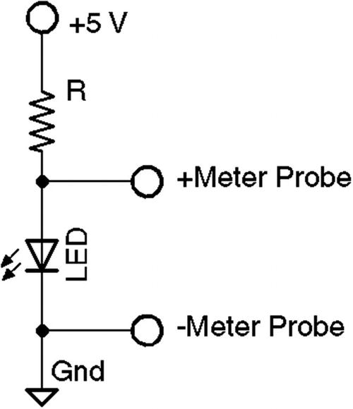
Measuring forward voltage (VF) of an unknown LED
Despite all the precaution of measuring the forward voltage, you may still compute the 10% resistor value of 220 or 330 ohms. But this gives you reassurance that no harm will occur to the GPIO. For higher voltage LEDs, the limiting resistor can be safely eliminated. If there is any doubt, measure the current consumed by the LED when it is on. It should not exceed 16 mA to stay within the Pi’s driving limit.
Driving Logic Interfaces
For LEDs, the requirements of the interface are rather simple. The interface is a success if the LED is lit when the output port is in one state, and the LED is dark in the other. The precise voltage appearing at the GPIO output pin in these two states is of little concern if the maximum current limits are respected.
When interfacing to logic, the output voltage is critical. For the receiving logic, the output level must be at least VIH to reliably register a 1 bit (for the BCM2835, this is 1.3 V). Likewise, the output should present less than VIL to reliably register a 0 in the receiver (for the BCM2835, this is 0.8V). Any voltage level between these limits is ambiguous and can cause the receiver to randomly see a 0 or a 1.
There are a large number of approaches to interfacing between different logic families. A good source of information is provided by the document “Microchip 3V Tips’n Tricks.”12 Another document titled “Interfacing 3V and 5V Applications, AN240” describes the issues and challenges of interfacing between systems.13 It describes, for example, how a 5 V system can end up raising the 3.3 V supply voltage if precautions are not taken.
Approaches to interfacing include direct connections (when safe), voltage-dividing resistors, diode resistor networks, and the more-complex op-amp comparators. There is a whole chapter devoted to the subject in “Custom Raspberry Pi Interfaces.”14 When choosing an approach, remember to consider the necessary switching speed of the interface.
Driving Bi-color LEDs
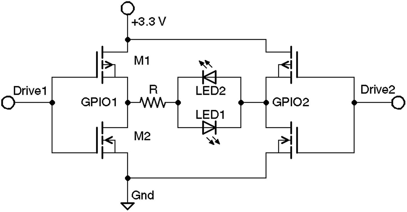
Driving a bi-color LED or LED pair
Truth Table for Driving Bi-color LEDs in Figure 11-6
GPIO-1 | GPIO-2 | Result |
|---|---|---|
Low | Low | Both LEDs are off (off) |
Low | High | LED2 is forward biased (on), LED1 is off |
High | Low | LED1 is forward biased (on), LED2 is off |
High | High | Both LEDs are off (off) |
The one complication to be aware of is that the VF of the different colored LEDs are likely to be quite different. You will need to compromise on the limiting resistor. Be sure that the GPIO output never needs to source or sink more than 16 mA.
Alternate Function
Alternate Function Selection
Code | Function Selected | ALT |
|---|---|---|
000 | GPIO pin is an input. | |
001 | GPIO pin is an output. | |
100 | GPIO pin is alternate function 0. | 0 |
101 | GPIO pin is alternate function 1. | 1 |
110 | GPIO pin is alternate function 2. | 2 |
111 | GPIO pin is alternate function 3. | 3 |
011 | GPIO pin is alternate function 4. | 4 |
010 | GPIO pin is alternate function 5. | 5 |
The values shown in the table’s Code column are used in the configuration register itself. The alternate function numbers are listed in the ALT column. Keeping these two straight can be confusing when programming. Once the function has been selected, the configuration is then fine-tuned according to its peripheral type.
Output Pins
Logic sense
Output state
The output state of the GPIO pins can either be set as a 32-bit word affecting 32 GPIOs at a time or set or cleared individually. Having individual set/clear operations allows the host to change individual bits without disturbing the state of others, or having to know their state.
Input Pins
Detect rising input signals (synchronous/asynchronous)
Detect falling input signals (synchronous/asynchronous)
Detect high-level signals
Detect low-level signals
Logic sense
Interrupt handling (handled by driver)
Choose no pull-up; use a pull-up or pull-down resistor
Once these choices have been made, it is possible to receive data related to input signal changes, or simply query the pin’s current state.
Floating Potentials
The unconnected GPIO input can “float” if there is no pull-up or pull-down resistor provided or configured. When the input is connected to a driving circuit, that circuit will provide a non-floating voltage level. The GPIO input uses a MOSFET transistor. The nature of that is that it is sensitive only to voltage (not current, like a bipolar transistor). So when the input is left unconnected, the GPIO input can sense voltages, including static electricity nearby (like a cat).
Output GPIO pins are clamped to the output level, which leaves the internal input transistor in a safe state. When a GPIO is configured as an input, it is normally best to configure it with a pull-up or pull-down resistance. This will pull the signal high or to ground. When otherwise left to float, the static electricity will be random and require the ESD (electrostatic discharge diodes) protection diodes to bleed away the charge.
Summary
This chapter has introduced a number of hardware traits of the Raspberry Pi GPIO. This gives you a solid foundation of its capabilities as well as its limitations. The design of the Pi allows considerable GPIO flexibility, from drive level, pull-up resistors and alternate functions.
The chapters following will introduce different ways of working with the GPIO ports, including direct access from a C program.