
THE FUTURE OF THE ARCHITECTURE
15.1. ADVANCED DSP AND SIMD SUPPORT IN ARMV6
15.1.1. SIMD Arithmetic Operations
15.1.3. Complex Arithmetic Support
15.1.4. Saturation Instructions
15.1.5. Sum of Absolute Differences Instructions
15.1.6. Dual 16-Bit Multiply Instructions
15.2. SYSTEM AND MULTIPROCESSOR SUPPORT ADDITIONS TO ARMV6
In October 1999, ARM began to consider the future direction of the architecture that would eventually become ARMv6, first implemented in a new product called ARM1136J-S. By this time, ARM already had designs for many different applications, and the future requirements of each of those designs needed to be evaluated, as well as the new application areas for which ARM would be used in the future.
As system-on-chip designs have become more sophisticated, ARM processors have become the central processors in systems with multiple processing elements and subsystems. In particular, the portable and mobile computing markets were introducing new software and performance challenges for ARM. Areas that needed addressing were digital signal processing (DSP) and video performance for portable devices, interworking mixed-endian systems such as TCP/IP, and efficient synchronization in multiprocessing environments. The challenge for ARM was to address all of these market requirements and yet maintain its competitive advantage in computational efficiency (computing power per mW) as the best in the industry.
This chapter describes the components within ARMv6 introduced by ARM to address these market requirements, including enhanced DSP support and support for a multiprocessing environment. The chapter also introduces the first high-performance ARMv6 implementations and, in addition to the ARMv6 technologies, one of ARM’s latest technologies—TrustZone.
15.1 ADVANCED DSP AND SIMD SUPPORT IN ARMv6
Early in the ARMv6 project, ARM considered how to improve the DSP and media processing capabilities of the architecture beyond the ARMv5E extensions described in Section 3.7. This work was carried out very closely with the ARM1136J-S engineering team, which was in the early stages of developing the microarchitecture for the product. SIMD (Single Instruction Multiple Data) is a popular technique used to garner considerable data parallelism and is particularly effective in very math-intensive routines that are commonly used in DSP, video and graphics processing algorithms. SIMD is attractive for high code density and low power since the number of instructions executed (and hence memory system accesses) is kept low. The price for this efficiency is the reduced flexibility of having to compute things arranged in certain blocked data patterns; this, however, works very well in many image and signal processing algorithms.
Using the standard ARM design philosophy of computational efficiency with very low power, ARM came up with a simple and elegant way of slicing up the existing ARM 32-bit datapath into four 8-bit and two 16-bit slices. Unlike many existing SIMD architectures that add separate datapaths for the SIMD operations, this method allows the SIMD to be added to the base ARM architecture with very little extra hardware cost.
The ARMv6 architecture includes this “lightweight” SIMD approach that costs virtually nothing in terms of extra complexity (gate count) and therefore power. At the same time the new instructions can improve the processing throughput of some algorithms by up to two times for 16-bit data or four times for 8-bit data. In common with most operations in the ARM instruction set architecture, all of these new instructions are executed conditionally, as described in Section 2.2.6.
You can find a full description of all ARMv6 instructions in the instruction set tables of Appendix A.
15.1.1 SIMD ARITHMETIC OPERATIONS
Table 15.1 shows a summary of the 8-bit SIMD operations. Each byte result is formed from the arithmetic operation on each of the corresponding byte slices through the source operands.
Table 15.1
8-bit SIMD arithmetic operations.
| Instruction | Description |
| SADD8{<cond>} Rd, Rn, Rm | Signed 8-bit SIMD add |
| SSUB8{<cond>} Rd, Rn, Rm | Signed 8-bit SIMD subtract |
| UADD8{<cond>} Rd, Rn, Rm | Unsigned 8-bit SIMD add |
| USUB8{<cond>} Rd, Rn, Rm | Unsigned 8-bit SIMD subtract |
| QADD8{<cond>} Rd, Rn, Rm | Signed saturating 8-bit SIMD add |
| QSUB8{<cond>} Rd, Rn, Rm | Signed saturating 8-bit SIMD subtract |
| UQADD8{<cond>} Rd, Rn, Rm | Unsigned saturating 8-bit SIMD add |
| UQSUB8{<cond>} Rd, Rn, Rm | Unsigned saturating 8-bit SIMD subtract |
The results of these 8-bit operations may require that up to 9 bits be represented, which either causes a wraparound or a saturation to take place, depending on the particular instruction used.
In addition to the 8-bit SIMD operations, there are an extensive range of dual 16-bit operations, shown in Table 15.2. Each halfword (16-bit) result is formed from the arithmetic operation on each of the corresponding 16-bit slices through the source operands.
Table 15.2
16-bit SIMD arithmetic operations.
| Instruction | Description |
| SADD16{<cond>} Rd, Rn, Rm | Signed add of the 16-bit pairs |
| SSUB16{<cond>} Rd, Rn, Rm | Signed subtract of the 16-bit pairs |
| UADD16{<cond>} Rd, Rn, Rm | Unsigned add of the 16-bit pairs |
| USUB16{<cond>} Rd, Rn, Rm | Unsigned subtract of the 16-bit pairs |
| QADD16{<cond>} Rd, Rn, Rm | Signed saturating add of the 16-bit pairs |
| QSUB16{<cond>} Rd, Rn, Rm | Signed saturating subtract of the 16-bit pairs |
| UQADD16{<cond>} Rd, Rn, Rm | Unsigned saturating add of the 16-bit pairs |
| UQSUB16{<cond>} Rd, Rn, Rm | Unsigned saturating subtract of the 16-bit pairs |
The results may need 17 bits to be stored, and in this case they can either wrap around or are saturated to within the range of a 16-bit signed result with the saturating version of the instruction.
Operands for the SIMD instructions are not always found in the correct order within the source registers; to improve the efficiency of dealing with these situations, there are 16-bit SIMD operations that perform swapping of the 16-bit words of one operand register. These operations allow a great deal of flexibility in dealing with halfwords that maybe aligned in different ways in memory and are particularly useful when working with 16-bit complex number pairs that are packed into 32-bit registers. There are signed, unsigned, saturating signed, and saturating unsigned versions of these operations, as shown in Table 15.3.
Table 15.3
16-bit SIMD arithmetic operations with swap.
| Instruction | Description |
| SADDSUBX{<cond>} Rd, Rn, Rm | Signed upper add, lower subtract, with a swap of halfwords in Rm |
| UADDSUBX{<cond>} Rd, Rn, Rm | Unsigned upper add, lower subtract, with swap of halfwords in Rm |
| QADDSUBX{<cond>} Rd, Rn, Rm | Signed saturating upper add, lower subtract, with swap of halfwords in Rm |
| UQADDSUBX{<cond>} Rd, Rn, Rm | Unsigned saturating upper add, lower subtract, with swap of halfwords in Rm |
| SSUBADDX{<cond>} Rd, Rn, Rm | Signed upper subtract, lower add, with a swap of halfwords in Rm |
| USUBADDX{<cond>} Rd, Rn, Rm | Unsigned upper subtract, lower add, with swap of halfwords in Rm |
| QSUBADDX{<cond>} Rd, Rn, Rm | Signed saturating upper subtract, lower add, with swap of halfwords in Rm |
| UQSUBADDX{<cond>} Rd, Rn, Rm | Unsigned saturating upper subtract, lower add, with swap of halfwords in Rm |
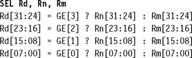
The X in the instruction mnemonic signifies that the two halfwords in Rm are swapped before the operations are applied so that operations like the following take place:
![]()
The addition of the SIMD operations means there is now a need for some way of showing an overflow or a carry from each SIMD slice through the datapath. The cpsr as originally described in Section 2.2.5 is modified by adding four additional flag bits to represent each 8-bit slice of the data path. The newly modified cpsr register with the GE bits is shown in Figure 15.1 and Table 15.4. The functionality of each GE bit is that of a “greater than or equal” flag for each slice through the datapath.
Table 15.4
| Field | Use |
| N | Negative flag. Records bit 31 of the result of flag-setting operations. |
| Z | Zero flag. Records if the result of a flag-setting operation is zero. |
| C | Carry flag. Records unsigned overflow for addition, not-borrow for subtraction, and is also used by the shifting circuit. See Table A.3. |
| V | Overflow flag. Records signed overflows for flag-setting operations. |
| Q | Saturation flag. Certain saturating operations set this flag on saturation. See for example QADD in Appendix A (ARMv5E and above). |
| J | J = 1 indicates Java execution (must have T = 0). Use the BXJ instruction to change this bit (ARMv5J and above). |
| Res | These bits are reserved for future expansion. Software should preserve the values in these bits. |
| GE[3:0] | The SIMD greater-or-equal flags. See SADD in Appendix A (ARMv6). |
| E | Controls the data endianness. See SETEND in Appendix A (ARMv6). |
| A | A = 1 disables imprecise data aborts (ARMv6). |
| I | I = 1 disables IRQ interrupts. |
| F | F = 1 disables FIQ interrupts. |
| T | T= 1 indicates Thumb state. T = 0 indicates ARM state. Use the BX or BLX instructions to change this bit (ARMv4T and above). |
| mode | The current processor mode. See Table B.4. |
Operating systems already save the cpsr register on a context switch. Adding these bits to the cpsr has little effect on OS support for the architecture.
In addition to basic arithmetic operations on the SIMD data slices, there is considerable use for operations that allow the picking of individual data elements within the datapath and forming new ensembles of these elements. A select instruction SEL can independently select each eight-bit field from one source register Rn or another source register Rm, depending on the associated GE flag.
These instructions, together with the other SIMD operations, can be used very effectively to implement the core of the Viterbi algorithm, which is used extensively for symbol recovery in communication systems. Since the Viterbi algorithm is essentially a statistical maximum likelihood selection algorithm, it is also used in such areas as speech and hand-writing recognition engines. The core of Viterbi is an operation that is commonly known as add-compare-select (ACS), and in fact many DSP processors have customized ACS instructions. With its parallel (SIMD) add, subtract (which can be used to compare), and selection instructions, ARMv6 can implement an extremely efficient add-compare-select:
![]()
This kernel performs the ACS operation on four paths in parallel and takes a total of 4 cycles on the ARM1136J-S. The same sequence coded for the ARMv5TE instruction set must perform each of the operations serially, taking at least 16 cycles. Thus the add-compare-select function is four times faster on ARM1136J-S for eight-bit metrics.
15.1.2 PACKING INSTRUCTIONS
The ARMv6 architecture includes a new set of packing instructions, shown in Table 15.5, that are used to construct new 32-bit packed data from pairs of 16-bit values in different source registers. The second operand can be optionally shifted. Packing instructions are particularly useful for pairing 16-bit values so that you can make use of the 16-bit SIMD processing instructions described earlier.
Table 15.5
| Instruction | Description |
| PKHTB{<cond>} Rd, Rn, Rm {, ASR #<shift_imm>} | Pack the top 16 bits of Rn with the bottom 16 bits of the shifted Rm into the destination Rd |
| PKHBT{<cond>} Rd, Rn, Rm {, LSL #<shift_imm>} | Pack the top 16 bits of the shifted Rm with the bottom 16 bits of Rn into the destination Rd |
15.1.3 COMPLEX ARITHMETIC SUPPORT
Complex arithmetic is commonly used in communication signal processing, and in particular in the implementations of transform algorithms such as the Fast Fourier Transform as described in Chapter 8. Much of the implementation detail examined in that chapter concerns the efficient implementation of the complex multiplication using ARMv4 or ARMv5E instruction sets.
ARMv6 adds new multiply instructions to accelerate complex multiplication, shown in Table 15.6. Both of these operations optionally swap the order of the two 16-bit halves of source operand Rs if you specify the X suffix.
Table 15.6
Instructions to support 16-bit complex multiplication.
| Instruction | Description |
| SMUAD{X}{<cond>} Rd, Rm, Rs | Dual 16-bit signed multiply and add |
| SMUSD{X}{<cond>} Rd, Rm, Rs | Dual 16-bit signed multiply and subtract |
EXAMPLE 15.1
In this example Ra and Rb hold complex numbers with 16-bit coefficients packed with their real parts in the lower half of a register and their imaginary part in the upper half.
We multiply Ra and Rb to produce a new complex number Rc. The code assumes that the 16-bit values represent Q15 fractions. Here is the code for ARMv6:
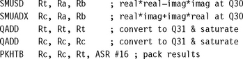
Compare this with an ARMv5TE implementation:
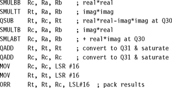
There are 10 cycles for ARMv5E versus 5 cycles for ARMv6. Clearly with any algorithm doing very intense complex maths, a two times improvement in performance can be gained for the complex multiply.
15.1.4 SATURATION INSTRUCTIONS
Saturating arithmetic was first addressed with the E extensions that were added to the ARMv5TE architecture, which was introduced with the ARM966E and ARM946E products. ARMv6 takes this further with individual and more flexible saturation instructions that can operate on 32-bit words and 16-bit halfwords. In addition to these instructions, shown in Table 15.7, there are the new saturating arithmetic SIMD operations that have already been described in Section 15.1.1.
Table 15.7
| Instruction | Description |
| SSAT Rd, #<BitPosition>, Rm,{<Shift>} | Signed 32-bit saturation at an arbitrary bit position. Shift can be an LSL or ASR. |
| SSAT16{<cond>} Rd, #<immed>, Rm | Dual 16-bit saturation at the same position in both halves. |
| USAT Rd, #<BitPosition>, Rm,{<Shift>} | Unsigned 32-bit saturation at an arbitrary bit position. Shift can be LSL or ASR. |
| USAT16{<cond>} Rd, #<immed>, Rm | Unsigned dual 16-bit saturation at the same position in both halves. |
Note that in the 32-bit versions of these saturation operations there is an optional arithmetic shift of the source register Rm before saturation, allowing scaling to take place in the same instruction.
15.1.5 SUM OF ABSOLUTE DIFFERENCES INSTRUCTIONS
These two new instructions are probably the most application specific within the ARMv6 architecture—USAD8 and USADA8. They are used to compute the absolute difference between eight-bit values and are particularly useful in motion video compression algorithms such as MPEG or H.263, including motion estimation algorithms that measure motion by comparing blocks using many sum-of-absolute-difference operations (see Figure 15.2). Table 15.8 lists these instructions.
Table 15.8
| Instruction | Description |
| USAD8{<cond>} Rd, Rm, Rs | Sum of absolute differences |
| USADA8{<cond>} Rd, Rm, Rs, Rn | Accumulated sum of absolute differences |
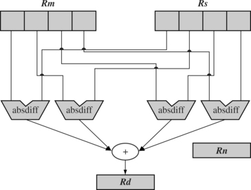
To compare an N × N square at (x, y) in image p1 with an N × N square p2, we calculate the accumulated sum of absolute differences:
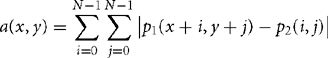
To implement this using the new instructions, use the following sequence to compute the sum-of-absolute differences of four pixels:
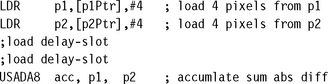
There is a tremendous performance advantage for this algorithm over an ARMv5TE implementation. There is a four times improvement in performance from the eight-bit SIMD alone. Additionally the USADA8 operation includes the accumulation operation. The USAD8 operation will typically be used to carry out the setup into the loop before there is an existing accumulated value.
15.1.6 DUAL 16-BIT MULTIPLY INSTRUCTIONS
ARMv5TE introduced considerable DSP performance to ARM, but ARMv6 takes this much further. Implementations of ARMv6 (such as ARM1136J) have a dual 16 × 16 multiply capability, which is comparable with many high-end dedicated DSP devices. Table 15.9 lists these instructions.
Table 15.9
Dual 16-bit multiply operations.
| Instruction | Description |
| SMLAD{X}{<cond>} Rd, Rm, Rs, Rn | Dual signed multiply accumulate with 32-bit accumulation |
| SMLALD{X}{<cond>} RdLo, RdHi, Rm, Rs | Dual signed multiply accumulate with 64-bit accumulation |
| SMLSD{X}{<cond>} Rd, Rm, Rs, Rn | Dual signed multiply subtract with 32-bit accumulation |
| SMLSLD{X}{<cond>} RdLo, RdHi, Rm, Rs | Dual signed multiply subtract with 64-bit accumulation |
We demonstrate the use of SMLAD as a signed dual multiply in a dot-product inner loop:
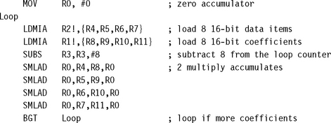
This loop delivers eight 16 × 16 multiply accumulates in 10 cycles without using any data-blocking techniques. If a set of the operands for the dot-product is stored in registers, then performance approaches the true dual multiplies per cycle.
15.1.7 MOST SIGNIFICANT WORD MULTIPLIES
ARMv5TE added arithmetic operations that are used extensively in a very broad range of DSP algorithms including control and communications and that were designed to use the Q15 data format. However, in audio processing applications it is common for 16-bit processing to be insufficient to describe the quality of the signals. Typically 32-bit values are used in these cases, and ARMv6 adds some new multiply instructions that operate on Q31 formatted values. (Recall that Q-format arithmetic is described in detail in Chapter 8.) These new instructions are listed in Table 15.10.
Table 15.10
Most significant word multiplies.
| Instruction | Description |
| SMMLA{R}{<cond>} Rd, Rm, Rs, Rn | Signed 32 × 32 multiply with accumulation of the high 32 bits of the product to the 32-bit accumulator Rn |
| SMMLS{R}{<cond>} Rd, Rm, Rs, Rn | Signed 32 × 32 multiply subtracting from (Rn << 32) and then taking the high 32 bits of the result |
| SMMUL{R}{<cond>} Rd, Rm, Rs | Signed 32 × 32 multiply with upper 32 bits of product only |
The optional {R} in the mnemonic allows the addition of the fixed constant 0×80000000 to the 64-bit product before producing the upper 32 bits. This allows for biased rounding of the result.
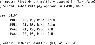
15.1.8 CRYPTOGRAPHIC MULTIPLICATION EXTENSIONS
In some cryptographic algorithms, very long multiplications are quite common. In order to maximize their throughput, a new 64 + 32 × 32 → 64 multiply accumulate operation has been added to complement the already existing 32 × 32 multiply operation UMULL (see Table 15.11).
Table 15.11
| UMAAL{<cond>} RdLo, RdHi, Rm, Rs | Special crypto multiply (RdHi : RdLo) = Rm * Rs + RdHi + RdLo |
Here is an example of a very efficient 64-bit × 64-bit multiply using the new instructions:
15.2 SYSTEM AND MULTIPROCESSOR SUPPORT ADDITIONS TO ARMv6
As systems become more complicated, they incorporate multiple processors and processing engines. These engines may share different views of memory and even use different endiannesses (byte order). To support communication in these systems, ARMv6 adds support for mixed-endian systems, fast exception processing, and new synchronization primitives.
15.2.1 MIXED-ENDIANNESS SUPPORT
Traditionally the ARM architecture has had a little-endian view of memory with a big-endian mode that could be switched at reset. This big-endian mode sets the memory system up as big-endian ordered instructions and data.
As mentioned in the introduction to this chapter, ARM has found its cores integrated into very sophisticated system-on-chip devices dealing with mixed endianess, and often has to deal with both little- and big-endian data in software. ARMv6 adds a new instruction to set the data endianness for large code sequences (see Table 15.12), and also some individual manipulation instructions to increase the efficiency of dealing with mixed-endian environments.
Table 15.12
Setting data-endianness operation.
| SETEND <endian_specifier> | Change the default data endianness based on the <endian_specifier> argument. |
The endian_specifier is either BE for big-endian or LE for little endian. A program would typically use SETEND when there is a considerable chunk of code that is carrying out operations on data with a particular endianness. Figure 15.3 shows individual byte manipulation instructions.
15.2.2 EXCEPTION PROCESSING
It is common for operating systems to save the return state of an interrupt or exception on a stack. ARMv6 adds the instructions in Table 15.13 to improve the efficiency of this operation, which can occur very frequently in interrupt/scheduler driven systems.
Table 15.13
Exception processing operations.
| Instruction | Description |
| SRS<addressing_mode>, #mode{!} | Save return state (lr and spsr) on the stack addressed by sp in the specified mode. |
| RFE <addressing_mode>, Rn{!} | Return from exception. Loads the pc and cpsr from the stack pointed to by Rn. |
| CPS<effect> <iflags> {,#<mode>} | Change processor state with interrupt enable or disable. |
| CPS #<mode> | Change processor state only. |
15.2.3 MULTIPROCESSING SYNCHRONIZATION PRIMITIVES
As system-on-chip (SoC) architectures have become more sophisticated, ARM cores are now often found in devices with many processing units that compete for shared resources.
The ARM architecture has always had the SWP instruction for implementing semaphores to ensure consistency in such environments. As the SoC has become more complex, however, certain aspects of SWP cause a performance bottleneck in some instances. Recall that SWP is basically a “blocking” primitive that locks the external bus of the processor and uses most of its bandwidth just to wait for a resource to be released. In this sense the SWP instruction is considered “pessimistic”—no computation can continue until SWP returns with the freed resource.
New instructions LDREX and STREX (load and store exclusive) were added to the ARMv6 architecture to solve this problem. These instructions, listed in Table 15.14, are very straightforward in use and are implemented by having a system monitor out in the memory system. LDREX optimistically loads a value from memory into a register assuming that nothing else will change the value in memory while we are working on it. STREX stores a value back out to memory and returns an indication of whether the value in memory was changed or not between the original LDREX operation and this store. In this way the primitives are “optimistic”—you continue processing the data you loaded with LDREX even though some external device may also be modifying the value. Only if a modification actually took place externally is the value thrown away and reloaded.
Table 15.14
Load and store exclusive operations.
| Instructions | Description |
| LDREX{<cond>} Rd, [Rn] | Load from address in Rn and set memory monitor |
| STREX{<cond>} Rd, Rm, [Rn] | Store to address in Rn and flag if successful in Rd (Rd = 0 if successful) |
The big difference for the system is that the processor no longer waits around on the system bus for a semaphore to be free, and therefore leaves most of the system bus bandwidth available for other processes or processors.
15.3 ARMv6 IMPLEMENTATIONS
ARM completed development of ARM1136J in December 2002, and at this writing consumer products are being designed with this core. The ARM1136J pipeline is the most sophisticated ARM implementation to date. As shown in Figure 15.4, it has an eight-stage pipeline with separate parallel pipelines for load/store and multiply/accumulate.
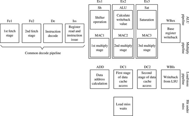
The parallel load/store unit (LSU) with hit-under-miss capability allows load and store operations to be issued and execution to continue while the load or store is completing with the slower memory system. By decoupling the execution pipeline from the completion of loads or stores, the core can gain considerable extra performance since the memory system is typically many times slower than the core speed. Hit-under-miss extends this decoupling out to the L1-L2 memory interface so that an L1 cache miss can occur and an L2 transaction can be completing while other L1 hits are still going on.
Another big change in microarchitecture is the move from virtually tagged caches to physically tagged caches. Traditionally, ARM has used virtually tagged caches where the MMU is between the caches and the outside L2 memory system. With ARMv6, this changes so that the MMU is now between the core and the L1 caches, so that all cache memory accesses are using physical (already translated) addresses. One of the big benefits of this approach is considerably reduced cache flushing on context switches when the ARM is running large operating systems. This reduced flushing will also reduce power consumption in the end system since cache flushing directly implies more external memory accesses. In some cases it is expected that this architectural change will deliver up to a 20% performance improvement.
15.4 FUTURE TECHNOLOGIES BEYOND ARMv6
In 2003, ARM made further technology announcements including TrustZone and Thumb-2. While these technologies are very new, at this writing, they are being included in new microprocessor cores. The next sections briefly introduce these new technologies.
15.4.1 TRUSTZONE
TrustZone is an architectural extension targeting the security of transactions that may be carried out using consumer products such as cell phones and, in the future, perhaps online transactions to download music or video for example. It was first introduced in October 2003 when ARM announced the ARM1176JZ-S.
The fundamental idea is that operating systems (even on embedded devices) are now so complex that it is very hard to verify security and correctness in the software. The ARM solution to this problem is to add new operating “states” to the architecture where only a small verifiable software kernel will run, and this will provide services to the larger operating system. The microprocessor core then takes a role in controlling system peripherals that may be only available to the secure “state” through some new exported signals on the bus interface. The system states are shown in Figure 15.5.
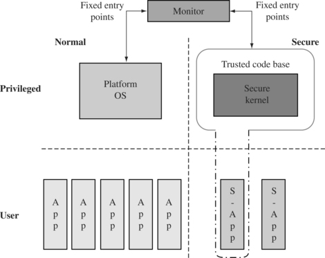
Figure 15.5 Modified security structure using TrustZone technology. Source: Richard York, A New Foundation for CPU Systems Security: Security Extensions to the ARM Architecture, 2003.
TrustZone is most useful in devices that will be carrying out content downloads such as cell phones or other portable devices with network connections. Details of this architecture are not public at the time of writing.
15.4.2 THUMB-2
Thumb-2 is an architectural extension designed to increase performance at high code density. It allows for a blend of 32-bit ARM-like instructions with 16-bit Thumb instructions. This combination enables you to have the code density benefits of Thumb with the additional performance benefits of access to 32-bit instructions.
Thumb-2 was announced in October 2003 and will be implemented in the ARM1156T2-S processor. Details of this architecture are not public at the time of writing.
15.5 SUMMARY
The ARM architecture is not a static constant but is being developed and improved to suit the applications required by today’s consumer devices. Although the ARMv5TE architecture was very successful at adding some DSP support to the ARM, the ARMv6 architecture extends the DSP support as well as adding support for large multiprocessor systems. Table 15.15 shows how these new technologies map to different processor cores.
Table 15.15
| Processor core | Architecture version |
| ARM1136J-S | ARMv6J |
| ARM1156T2-S | ARMv6 + Thumb-2 |
| ARM1176JZ-S | ARMv6J + TrustZone |
ARM still concentrates on one of its key benefits—code density—and has recently announced the Thumb-2 extension to its popular Thumb architecture. The new focus on security with TrustZone gives ARM a leading edge in this area.