
Modelling thin film deposition processes based on real-time observation
Abstract:
we introduce time and length scales of growth processes and then review experimental techniques for real-time and in-situ studies. In particular, we discuss optical monitoring techniques, time resolved microscopy, and real-time scattering techniques (X-ray, He-, and electron scattering). For scattering experiments we discuss details of the analysis, in particular anti-Bragg growth oscillations as observed in X-ray- and He-scattering as well as RHEED. we illustrate real-time observation and modelling of thin film deposition with examples from organic molecular beam deposition.
5.1 Introduction: time resolved surface science
As is evident from the various chapters in this book, thin film growth has many different facets to it, and growth is inherently a non-equilibrium and time-dependent phenomenon. While the investigation of the final product, i.e. the grown film, with its structure and morphology, may allow one to partially reconstruct the growth process, frequently the real-time observation of the growing film is required to fully characterize and understand the growth in its complexity. This is particularly evident if transient phenomena occur during the growth. In this chapter, after a brief discussion in Section 5.2 of some concepts of growth and the associated time scales, we present first an overview of various techniques (Section 5.3) for real-time studies including microscopy, optical spectroscopy, and scattering and indicate their strengths and weaknesses. Scattering techniques are discussed at some length, since they are at the center of most of the case studies in Section 5.4.
For the foundations of growth and its theoretical background we refer to other chapters in this book as well as earlier books and reviews (e.g., Venables, 2000; Venables et al., 1984, Zangwill, 1988; Pimpinelli and Villain, 1998; Barabási and Stanley, 1995; Michely and Krug, 2004; Krug, 1997). For the purpose of coherence, the case studies are mostly based on our own work on systems from organic molecular beam deposition (OMBD) (Witte and Woll, 2004; Schreiber, 2004; Forrest, 1997), but it is important to stress that the concepts outlined here can be very easily transferred to other, of course also inorganic, systems. It is clear that within the scope of this chapter the references cannot be exhaustive, but with those given it should be possible to trace a more complete list of references on a given subject.
5.2 Basics of growth and relevant length of and timescales for in-situ observation of film deposition
Growth phenomena are extremely rich and include a number of competing processes. Adsorption and desorption processes are followed by thermalisation and diffusion on the surface terrace. Adatoms can form a new crystal grain, attach to an existing one, or cross a step-edge onto a different terrace. Depending on the relative probabilities of these different processes, the growth mode varies between layer-by-layer growth (Frank–van-der-Merwe), layer-by-layer plus island growth (Stranski–Krastanov), or island growth (Volmer–Weber). Not only the growth mode but also the morphology of the thin film varies greatly as the island size and shape depends on the above processes, leading for example to fractal morphology for diffusion limited aggregation.
An important issue in the context of experimental real-time observations of growth and the modelling of these processes is the issue of time and length scales. Length scales in growth range from 10− 12-10− 3 m: the (sub-)atomic length scales determine strain and lattice parameters, diffusion length scales often range in the mm length scale, and, depending on the growth mode, macroscopic crystallite sizes are possible. Further relevant length scales are the surface roughness σ, in-plane correlation length ξ and island sizes, which often change during growth. Time resolved techniques offer the particular advantage that the dependence of length scales on film thickness d can be followed and directly compared to, for example, theoretical scaling models, which describe the time/thickness dependence by scaling laws using the roughening exponent β and the dynamic exponent z (Krug, 2004):

Similarly, growth processes span many orders of magnitude from ultra-fast to hour-long timescales. In the following sections we will discuss experimental techniques with a time resolution from μs to hours, which make it possible to study some of the most important aspects of growth. To give an overview of processes occurring during growth, Figure 5.1 shows both ultra-fast and slow timescales.
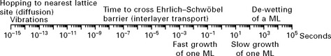
Atomistic processes that underlie and determine the growth behaviour occur on ultra-fast timescales in the picosecond range. Thermalisation of the adsorbed atoms/molecules occurs via transfer of translational and rotational energy to phonon modes of the substrate and, in the case of molecular adsorbates, also into internal molecular vibrations. Typical oscillation periods lie in the range of tens of femtoseconds (an example being the 515 cm− 1 Raman line of silicon) up to picoseconds for large molecules. The frequencies of these (surface phonon) modes often coincide with the typical attempt frequencies assumed in Monte Carlo simulations for diffusion and hopping processes. Intuitively it seems plausible to make a connection between a vibrational frequency and the frequency of attempts Γ0 to surmount, for example, a step-edge barrier Eb according to an Arrhenius relation for the process rate k:
Indeed, a timescale of around 1 ps (i.e., 1 THz) has typically been measured in experiments and deduced in density functional theory (Ratsch and Scheffler, 1998) but it is important to note that there are also other effects such as motion of a whole cluster of adatoms/admolecules, where the attempt frequency is changed due to collective effects.
Even though the atomic/molecular movement is ultra-fast and the attempt frequency very high, the often substantial energy barriers for diffusion slow down the rates by many orders of magnitude. One mechanism of surface diffusion is hopping of atoms to the nearest neighbour lattice site, while collective movements such as dimer and cluster diffusion are often neglected. For the energy barrier Ed for hopping, values of around 100 meV (e.g., 100 meV for Ag on Ag(111) (Brune et al., 1995), 20 meV for sexiphenyl (Hlawacek et al., 2008) and 80 meV for PTCDA (Fendrich and Krug, 2007)) were reported. of course, these strongly depend on the given system. The diffusion parameter D then is related to the hopping rate by
with l being the jump length and α depending on the dimensionality and symmetry of motion (α = 2 for a square lattice). Similarly to surface diffusion, also the diffusion across a step-edge is hindered by the so-called Ehrlich–Schwöbel barrier Eb (Ehrlich and Hudda, 1966, Schwoebel and Shipsey, 1966), which is crucial in determining the growth morphology of the thin film (Markov, 2004, Trofimov and mokerov, 2002). Typical values of Eb are in the range of several 100 meV: 139 meV for Ag(111) (Haftel, 2001), 670 meV for sexiphenyl (Hlawacek et al., 2008), and 750 meV for PTCDA (Fendrich and Krug, 2007). For a sample at room temperature these step-edge barriers are large compared to kBT so that crossing a step-edge is comparatively slow. Depending on the height of the barrier, the time for an atom to move down to the layer underneath (the inverse of the rate constant for crossing a step) can then range from 10 ps to 1 s, the large spread being due to the exponential dependence on the barrier height (see Fig. 5.1). In general the diffusion and step-edge barriers depend on the orientation of the underlying crystal and, unlike homoepitaxy, for thin film growth the Ehrlich–Schwöbel barrier can also be layer dependent, e.g. due to strain (Zhang et al., 2009, Krause et al., 2004a).
Through rate limiting steps, such as step-edge diffusion or nucleation, which at moderate temperatures are very slow or even completely frozen out, fast processes can be slowed down to relatively long timescales (see Fig. 5.1). Apart from such material-specific, intrinsic effects, extrinsic parameters start to play a role for slower processes. The most important extrinsic parameter regarding timescales is the growth rate, which is the net flux of atoms/molecules onto a surface. The growth rate determines the time to form a monolayer and therefore is the reference timescale for real-time experiments. This monolayer formation time can range from milliseconds for technological production processes up to many seconds or even hours in research. Such slow rates are mostly employed in fundamental research, as production processes have to be optimized for high throughput, so that also fast time-resolved experimental techniques are necessary or have to be developed for production monitoring. Further, the structure and morphology of the growing thin film itself can depend strongly on the growth rate, as fast kinetic growth can result in structures far from thermodynamic equilibrium if the formation of the lowest energy structure is slow.
In conclusion, growth phenomena span an extremely wide range of timescales, so far inaccessible to any single theory or experiment. Ultra-fast studies are used to determine the basic atomistic processes and calibrate rate constants used in theory. Experiments at slower timescales are very important to identify the growth scenario and follow the structure formation, strain, and morphology. It is remarkable how experiments on the second time-scale can help to deduce information on atomistic processes on the surface. Further, real-time experiments are also important technologically, because growth monitoring greatly facilitates or even enables growth of complicated nano- or hetero-structures which could not be grown without direct process control.
5.3 Experimental techniques for real-time and in-situ studies
Experimental techniques for real-time and in-situ studies face several challenges. Ideally, a wide range of timescales has to be studied, structural details have to be resolved on atomic length scales in the growth direction and on the length scale of growing islands in the in-plane direction, the observation should not interfere with growth itself, and the techniques have to be surface sensitive, that is they have to discern the small surface signal of a (monolayer) thin film from the substrate signal. Currently, no single technique is able to follow individual atomic movements on both ultra-fast and slow timescales. Correspondingly, several experimental techniques are necessary to study different time- and length scales. Without claiming to be exhaustive, Fig. 5.2 gives an overview of different techniques used for real-time measurements.
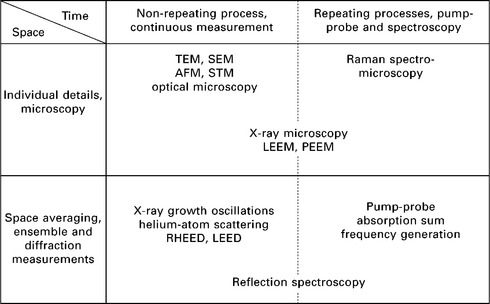
5.2 Simplified overview of techniques for real-time growth observation. The boundaries are, of course, not always necessarily sharp. Details of the techniques shown can be found in technique oriented chapters in this book and Lüth (2001) and Michely and Krug (2004).
A distinction has to be made between ensemble averaging measurements and individual measurements both in space and time. In the spatial domain, ensemble measurements such as X-ray scattering provide atomic detail averaged over a certain sample area, while microscopy techniques are able to resolve individual atomic or molecular details, albeit usually at slower time resolution. Similarly, in the time domain it is possible to distinguish between continuous real-time measurements that resolve single configurations of an on-going process on the one hand, and pump-probe or spectroscopy techniques which average over many repetitions of an ultra-fast/oscillatory process on the other (note that the data acquisition time is much longer than the process under study). Growth processes in general are non-repetitive and hard to reset or trigger by external stimuli (an exception being pulsed laser deposition; Ferguson et al., 2009; Tischler et al., 2006), so that pump-probe techniques do not easily lend themselves to in-situ growth studies. Therefore, ultra-fast time resolution is hard to achieve in growth studies, because a continuous measurement is limited by the read out speed of electronics, and, even more severely, by the time needed to acquire sufficient measurement statistics without averaging. Despite a continuous measurement on slow timescales, absorption or Raman spectroscopy also contain spectroscopic information on ultra-fast vibrational timescales of damped oscillatory processes.
In the following we will not discuss ultra-fast techniques but focus on methods that can be used for real-time measurements during growth without temporal averaging. Microscopy techniques have started to become fast enough for real-time observation and examples of LEEM (Meyer Zu Heringdorf et al., 2001) or STM microscopy (Rost, 2007) show the potential of spatially resolved measurements. Nevertheless, most real-time experiments in process monitoring and basic research average over a representative sample area. Widespread techniques in both engineering and research environments are real-time reflectance/ellipsometry measurements and reflection high-energy electron diffraction (RHEED) oscillations, because of the comparative simplicity of the setup. Real-time X-ray scattering and real-time helium atom scattering are more complex experimental setups, but yield different information. The latter techniques can also be applied to different types of samples such as molecular materials, which may get damaged by high-energy electrons. In the following we will give an overview of spectroscopic and microscopic techniques for growth monitoring, and then discuss and compare helium atom, electron and X-ray scattering. We will focus on the issues conceptually relevant in the context of real-time observations and their modelling. We will not attempt to explain the implications in terms of experimental technology and rather refer to the works of Forker and Fritz (2009), Lüth (2001) and Poelsema and Comsa (1989).
5.3.1 Optical spectroscopy techniques
Optical spectroscopy techniques can detect sub-monolayers of molecular/atomic adsorbates on substrates (Forker and Fritz, 2009; Heinemeyer et al., 2010). In differential reflectance spectroscopy (DRS), spectroscopic information is gathered by acquiring the reflectivity R of the substrate before and during deposition of a thin film usually at normal incidence. The time dependent DRS signal is then calculated according to
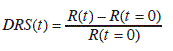
where R(t = 0) corresponds to the reflectivity of the bare substrate and R(t) to the reflectivity at time t of the deposition when the substrate is covered by the film with thickness d. As a high photon flux measurement the detector sensitivity and dark count rate is often less crucial than high dynamic range and fast read-out speeds (typically ~10 ms). A typical time resolution is below 10 s, taking into account averaging of multiple spectra to obtain low coverage sensitivity. At normal incidence and for very thin films (i.e. for d/λ < < 1) on a transparent substrate with refractive index n the DRS signal can be related directly to the imaginary part ε2 of the dielectric function according to Mclntyre and Aspnes (1971):
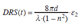
This approximation simplifies the analysis greatly, although it is not possible to determine ε1.For thicker films, the complete dielectric function (ε1 + ε2) can be modelled by matrix method based software. The experimental set up for in-situ DRS is shown in Fig. 5.3.
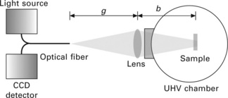
5.3 Experimental setup for in-situ DRS (Heinemeyer, 2009).
Expanding the capabilities of DRS, reflection anisotropy spectroscopy (RAS) measures the reflectance at normal incidence for two perpendicular polarisations of light and therefore can also resolve in-plane anisotropies of the optical constants (Weightman et al., 2005; Hartell et al., 2001). Spectroscopic ellipsometry (Arwin and Aspnes, 1984; Aspnes et al., 1990) finally expands polarisation sensitive measurements to a range of different incidence angles and therefore can also determine film thicknesses in the nm range, that is far below the wavelength of light.
Typical information that can be obtained from real-time optical spectroscopy is the film thickness evolution, and spectral changes due to different structures that form during growth. The structural information is only indirectly inferred from models that describe the excited states in the thin film. Therefore structural probes such as scattering techniques are sometimes preferable as a direct measurement technique (Lazzari et al., 2009; Hosokai et al., 2010). Nevertheless, ellipsometry, DRS and RAS can be used as a fingerprint technique if the connection between structure and spectral features is known. Further, optical functional properties such as the optical bandgap can be determined and correlated with the changes in thin film structure during growth.
5.3.2 Microscopy
Microscopy techniques are a direct way to measure the real-space structure of a growing thin film, but at the same time most microscopy setups also severely restrict the growth environment so that they are not commonly used as standard process characterisation tools. Usually, a trade-off between temporal resolution and spatial resolution has to be found in particular for scanning microscopy techniques. Nevertheless, they combine desirable experimental properties such as observation of individual sample features in both space and time.
Scanning probe microscopy (SPM)
Scanning probe techniques have enjoyed tremendous popularity in thin film studies due to their atomic resolution capabilities and compatibility with vacuum, gas, and liquid environments. An advantage of SPM is the imaging of growth morphologies in real space, in particular island shapes, nucleation sites and nucleation densities (Rabe and Buchholz, 1991; Fischer et al., 1999; Rusponi et al., 1997, Kneppe et al., 2000). Growth studies have been performed for solution deposition (e.g., Hyde et al., 2002; Rabe and Buchholz, 1991) with a time resolution down to video rate (~30 ms). Great care has to be taken that the atomic force microscopy (AFM) tip does not disturb growth nuclei, for example by avoiding contact mode and scanning in tapping mode.
STM measurements with, in principle, atomic resolution have also been used for in-situ growth studies on moderately well conducting substrates. Au deposition from an evaporation source in vacuum has been studied by Rost (2007) and atomic-height steps could be imaged with a lateral resolution of 1 nm in a field of view of 500 × 500 nm. Such a real-time dataset giving microscopic insight into growth with atomic resolution makes it possible to watch growth modes such as step flow and nucleation at dislocations directly. Great care has to be taken to avoid a disturbance of the growth, for example by shadowing the atomic flux with the tip, or coating of the tip itself with the evaporation material, which may either influence the shape of the tip or also lead to atoms diffusing from the tip onto the surface.
In conclusion, real-time STM studies are slightly challenging but gaining popularity due to technical advances. Since the focus in this chapter is on scattering techniques, for an in-depth discussion the reader is referred to Hofer et al. (2003) and references therein.
Electron microscopy
Electron microscopy combines good spatial resolution and a wide field of view for acquiring some surface statistics with video rate (30 ms) real-time capabilities. The best spatial resolution is obtained in transmission electron microscopy (TEM), albeit at the expense of restricting the sample to very thin substrates in the range of several 10 nm and requiring the growth apparatus to fit in the microscope. Examples of real-time TEM studies include growth of cu on Au in a liquid cell from solution studied at 5 nm lateral resolution (Williamson et al., 2003) and formation of Pt nanoparticles in solution at sub-nm resolution (Zheng et al., 2009). Achieving not only structural resolution but also chemical imaging is highly desirable and X-ray fluorescence in TEM can provide additional, local chemical information but also imaging of photoelectrons gives a material-specific contrast. In-situ photoelectron emission microscopy (PEEM) at a time resolution of 60 s has been used to study growth of the molecular semiconductor pentacene. Using PEEM to study pentacene growth the diffusion limited dendritic growth of individual monolayers could be resolved down to 125 nm (Meyer Zu Heringdorf et al., 2001).
5.3.3 Scattering methods
Elastic X-ray scattering, atom scattering and electron scattering are particularly useful for real-time observation of thin films, because they give structural information on the atomic length scale with a time resolution suited to growth dynamics. They are compatible with typical vacuum growth environments and, in particular, X-rays with their large penetrating power can be used to perform experiments in a wide range of sample environments such as vacuum, gas and liquid environments. All three scattering techniques measure an ensemble average where usually:
but the spatial resolution, which is given by the (de Broglie) wavelength, can be on an atomic length scale (for a more precise discussion of resolution, see Fenter, 2002) so that area averaged microscopic properties are sampled. Spreading the X-ray or particle flux over a macroscopic area reduces the likelihood of beam damage while at the same time providing enough flux for obtaining sufficient counting statistics with a time resolution in the subsecond range.
We will first point out common characteristics of real-time measurements with X-ray, He-atoms, and electrons before individually discussing their unique properties. In general, a part of the incident beam changes the propagation direction, and the two wave vectors kin of the incident and kout of the scattered beam define the scattering plane (see Fig. 5.4). The wave vector transfer q = kout − kin points in the direction in which the periodicity d of the thin film is sampled, and strong reflections occur when the Bragg condition q = n2π/d is fulfilled for an integer n. Both the in-plane structure (q|| to the substrate surface, Fig. 5.4b) and out-of-plane structure (q⊥ to the sample surface along the growth direction, Fig. 5.4a) can be measured during growth. An example for following the in-plane structure is given in Section 5.4 and an observation of the in-plane reflections has been used for example in Schreiber et al. (1998), Schreiber (2000) and Kowarik et al. (2006) to follow the growth of self-assembled monolayers and other systems. There are several approaches for real-time structure analysis by scattering techniques. For instance, one can measure the (monotonous)increase or shift of a diffraction feature. Another approach is recording an oscillatory signal due to the filling of individual layers.
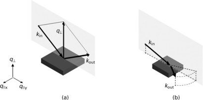
5.4 (a) Specular reflectivity measurement: incoming and outgoing beams enclose the same angle with the substrate surface, and therefore the wave vector transfer q is directed along the surface normal. (b) Grazing incidence diffraction (GIXD) and non-specular scattering involves a momentum transfer parallel to the surface.
Oscillating signals that vary with the number of lattice planes filled during growth are of particular interest and most commonly used, because details about the growth mode can be obtained with sub-monolayer resolution. For all three scattering techniques oscillations are primarily, but not exclusively, measured by observing the specular reflection, that is the scattered beam is detected for ‘mirror-like’ reflection (q⊥ perpendicular to sample surface). For the purpose of the following discussion, here we want to distinguish two basic scattering mechanisms, which influence the specular reflection signal during growth and may lead to intensity oscillations:
(a) Out-of-phase interference between the scattering from successively growing atomic monolayers (no change in in-plane momentum q|| = 0) (see Fig. 5.5a).
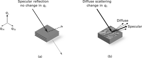
(b) Loss of specular intensity into diffuse scattering ‘sideways’ of the specular beam due to surface corrugation that oscillates during growth q|| ≠ 0) (see Fig. 5.5b).
In (a) the oscillations involve interference between atomic layers in different depths scattering out-of-phase, that is q⊥ must not fulfil the Bragg condition. Then the successive filling of atomic layers will cause the specular reflectivity to oscillate according to:
This equation adds the scattering amplitudes Asubstrate and An of both the substrate and all the n adlayers, taking into account the correct relative phase φ = q⊥d0 between the substrate and the adlayers due to d0 (bonding distance between substrate and first adlayer) as well as the phase shift between adlayers separated by a distance of n times the lattice constant d. The oscillations can be most readily understood for q⊥ = π/d where the exponential factor in the sum alternates between − 1 and 1, that is adjacent layers alternate between adding to/subtracting from the scattering amplitude. Note, that this mechanism only redistributes intensity between the reflected beam and the transmitted (and eventually absorbed) beam, because the in-plane wave vector is not changed – no in-plane periodicity is probed in this oscillation mechanism. Therefore in elastic scattering where momentum is conserved the only choice for q is being normal to the surface for the reflected beam or zero for the transmitted beam.
In (b) the mechanism of intensity change during growth (monotonous or oscillatory) is distinctly different as it involves momentum transfer not only perpendicular but also parallel to the sample surface. In case of a periodicity within the surface non-specular scattering can lead, inter alia, to in-plane Bragg reflections, while a non-periodic corrugated surface results in broad, diffuse scattering in many directions. while the surface changes during growth also the specularly and diffusely scattered signal change in a characteristic fashion. For all three techniques of X-ray, He, and electron scattering a changing surface corrugation – for example smooth → rough (upon nucleation of islands in a new layer) → smooth (upon layer completion) – leads to an oscillation in the diffuse scattered intensity (integrated over all q) with oscillating roughness (Fuoss et al, 1992; Eres et al., 2002). The specular reflection intensity changes inversely to the diffuse intensity, because beam intensity which is scattered diffusely is missing in the specular reflectivity.
It is important to note that in X-ray scattering also buried layers including the substrate contribute to the scattering, that is An is proportional to θn with θn being the coverage of the n-th layer. In contrast, for surface sensitive helium atom scattering, only the exposed layers contribute to the scattering, that is the scattering amplitudes An of buried layers vanish and An is proportional to the uncovered fraction (θn − θn − 1) of the n-th layer which also influences the oscillation period,
The underlying reasons (a) and (b) for growth oscillations are similar in all three techniques, but there are also important differences between the three probe types. Most importantly, the scattering cross-section and penetration depth varies greatly (see Fig. 5.6). Due to these different interaction mechanisms there are a range of differences in the real-time data which are discussed separately in the following sections.
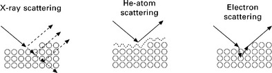
5.6 X-ray scattering penetrates the sample so that scattering occurs also from buried layers, while He-scattering is exclusively surface sensitive. Electron scattering occurs in the first few atomic layers and multiple scattering events can occur as shown.
X-ray scattering
X-ray scattering is usually performed at X-ray energies around 10 keV where the elastic scattering cross section is large and the wavelength of around 1 Å fits to studies of thin film growth on atomic length scales. It is worth noting that chemically selective scattering can be achieved by tuning the X-ray energy to specific atomic transitions where the scattering cross section is enhanced by anomalous scattering. In general, X-rays have great penetrating power so that not only the top surface is sampled, but also bulk lattice constants and buried interfaces are accessible.
Surface specificity can nevertheless be improved by using a grazing angle of incidence, so that the beam undergoes total external reflection and the X-ray intensity of the evanescent wave decays exponentially on a length scale of around 10–100 Å (depending on the film electron density) thereby reducing bulk sensitivity. This grazing incidence X-ray diffraction (GIXD) is used to determine in-plane lattice constants by scanning q||, and it can also be used to determine the thin film unit cell if so called rod scans are performed, that is the scattering vector is chosen to have components both in q|| and q⊥. GIXD has been performed in real time during growth of organic molecular semiconductors (Kowarik et al., 2009a) and makes it possible to follow structural changes and strain with a resolution below 0.01 Å− 1 with a time resolution of < 30 s.
Specular reflectivity measurements, for which q changes only along the surface normal, is useful to resolve changes along the surface normal, which usually coincides with the direction of growth. Experiments are typically performed at the Bragg condition to monitor the phase content, or at half the Bragg q vector which corresponds to the out-of-phase anti-Bragg condition. Both the Bragg reflection of a thin film and the reflectivity at the anti-Bragg point are usually weak enough that the kinematic approximation can be employed (the approximation breaks down close to the total reflection edge or at a strong Bragg reflection). Adapted to X-ray scattering which does not exclusively scatter at the surface but penetrates into the substrate, Eq. 5.6 can be rewritten using the form factor of the adlayer f(q):
Note that the substrate scattering amplitude and phase is fixed in time, and for the purpose of the time-dependent growth studies (i.e., θn(t) and the temporal change of the resulting scattering intensity) it is not important that Asubstrate may actually have to be calculated using dynamical theory.
For crystalline substrates the phase between substrate and thin film is given by Φ = d0q⊥ where d0 is the distance between the substrate surface (not the physical surface, but the last lattice plane). The binding distance d0 is an important parameter to understand interface properties such as charge carrier injection. The binding distance has been determined according to Eq. 5.7 in Alonso et al. (2003) which can be related to other techniques such as X-ray standing waves (Gerlach et al., 2005, 2007; Koch et al., 2008, Mercurio et al., 2010, Yamane et al., 2010).
The reflectivity for both homoepitaxy and heteroepitaxy has been calculated according to Eq. 5.7 and is shown in Fig. 5.7. In homoepitaxy the reflectivity is maximised when the surface is perfectly flat, that is the top monolayer is completely closed. When the next layer nucleates on top, the reflectivity drops and the relative change is greatest at the anti-Bragg condition, but other points in q-space oscillate with the same periodicity and may be more convenient (Krug et al., 2006). The intensity of the reflectivity at this anti-Bragg point oscillates with a periodicity of one monolayer for perfect layer-by-layer growth (Stephenson et al., 1999; Tischler et al., 2006; Van Der Vegt et al, 1995).
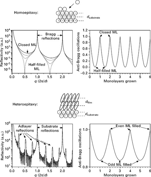
5.7 X-ray reflectivity curves (left) and growth oscillations (right) for homoepitaxy (top) and heteroepitaxy (bottom). In the simulation, perfect layer-by-layer growth is assumed. The model for heteroepitaxy consists of substrate with layer spacing dSubstrate and nine layers with a layer spacing of dfilm.
In heteroepitaxy the reflectivity in Fig. 5.7 is modified by the occurrence of additional Bragg reflections resulting from the overlayer and also interference fringes from reflections of the top and bottom interface of the film (Laue fringes) are visible. Further, it is important to note that the oscillation period at the anti-Bragg condition with respect to the overlayer is now changed from one monolayer to two monolayers, and the oscillation period depends on q (Weschke et al., 1997, Kowarik et al, 2009c). Indeed the shape of growth oscillations depends strongly on the substrate scattering amplitude and the relative phase as shown in Fig. 5.8. Compared to the case of vanishing substrate scattering, the growth oscillation amplitude can be increased if the substrate amplitude is in phase. Additional smaller scattering maxima can occur if substrate and film are out of phase. Homoepitaxy is a special case of the substrate amplitude being 180° out-of-phase and half as strong as the thin-film scattering (Dale et al., 2008).
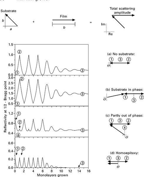
5.8 Simulation of anti-Bragg (= 1/2–Bragg) oscillations including substrate scattering (Kowarik et al., 2009c).
This selection of growth oscillation phenomena can be explained by the out-of-plane interference along q⊥ which leaves q|| unchanged (model (a) above). The diffuse scattering of the surface has been neglected so far because the modulation of the out-of-plane interference is usually stronger than the diffuse scattering amplitude. For some systems the diffuse scattering, while still weaker than the specular growth oscillations, contributes to the observed oscillation amplitude (Fleet et al., 2006). In conclusion, X-ray scattering offers a wide range of techniques to monitor growth experiments in real time, and due to the applicability of the kinematic scattering theory for most applications the interpretation is possible with the equations given above.
Helium atom scattering
In He atom scattering (HAS) the energy Ei of the impinging atoms is typically in the 10–100 meV range and therefore the de Broglie wavelength ![]() is in the range of 0.5–1.5 Å which is suitable for studying atomic length scales (Scoles et al., 1988). This energy is several orders of magnitude lower than the energy of electrons or photons at comparable energies, and therefore HAS avoids thermal or electronic excitation of the sample. The HAS energy scale of 10–100 meV is comparable to typical surface phonon energy- and timescales, and therefore inelastic scattering in HAS is an important tool to simultaneously sample dynamic surface processes as well as surface structure (Santoro et al., 1987; Witte and Wöll, 1995).
is in the range of 0.5–1.5 Å which is suitable for studying atomic length scales (Scoles et al., 1988). This energy is several orders of magnitude lower than the energy of electrons or photons at comparable energies, and therefore HAS avoids thermal or electronic excitation of the sample. The HAS energy scale of 10–100 meV is comparable to typical surface phonon energy- and timescales, and therefore inelastic scattering in HAS is an important tool to simultaneously sample dynamic surface processes as well as surface structure (Santoro et al., 1987; Witte and Wöll, 1995).
Another example of such energy-resolved scattering quasi-elastic heliumatom scattering (QHAS), where the adsorbate particles moving on the surface create a moving target and therefore the helium atoms experience a small change in velocity (Frenken et al., 1988). In QHAS studies the activation energy and the attempt frequency of surface diffusion have been determined and with spin echo techniques processes on timescales shorter than 0.5 μs can be detected as discussed in the review by Jardine et al. (2002).
Elastic HAS is also employed for structural analysis and growth oscillations, because He interacts through long range van-der-waals forces with the sample and the cross section is large compared to X-ray and electron scattering, which makes HAS extremely surface sensitive. (Ellis et al., 1995; Kern et al., 1991). Therefore, the helium atoms do not penetrate the surface but get reflected 3–4 Å (depending on the kinetic energy) above the surface. Due to the large cross sections this technique is sensitive to very low coverages, such as hydrogen adatoms with a density of 1/1000 of a monolayer (Poelsema and Comsa, 1989). Elastic helium atom scattering cannot probe bulk lattice constants, as it is exclusively surface-sensitive, but it has been used to measure surface step heights (Dastoor and Allison, 2003) and is very well suited to measuring step-edge densities and faceting (Hinch et al., 1990).
Real-time oscillations during growth and also the sputtering of a surface as ‘reverse growth’ have been studied with HAS for a wide range of systems (Farias and Rieder, 1998; Poelsema and Comsa, 1989). As the number of step-edges oscillates with the roughness development, so does the reflectivity of the surface according to mechanism (b) above, and indeed growth oscillations at the in-phase condition have been observed (Poelsema et al., 1992; Farias and Rieder, 1998). Nevertheless, stronger oscillations are observed for the out-of-phase/anti-phase condition, which is mostly used in HAS growth studies and usually interpreted with the destructive interference between adjacent layers similar to mechanism (a) above. In surface scattering this leads to the oscillation period of one monolayer, because the maximum reflection of a smooth surface is diminished by the destructively interfering next monolayer until the coverage is 50%; for higher coverages the lower lying layer interferes less with the top layer until a maximum is reached again for a closed top layer. A theoretical explanation for the oscillating reflection width/intensity is given in Poelsema and Comsa (1989). For a more detailed discussion on the different information that can be learned from in-phase and anti-phase oscillations, see Poelsema et al. (1992) and Xu et al. (1991).
Electron scattering
Electron scattering is one of the most common structural probes used in UHV growth systems, because the experimental setup is simpler than X-ray or HAS real-time experiments. The wavelength is again given by thedeBroglie wavelength, which for electrons can be written as ![]() In low energy electron diffraction (LEED) the electron energy is chosen to be in the range of 20–200 eV where the surface sensitivity is greatest due to the minimal penetration length of around 5–10 Å in this energy range (Braun, 1999, Oura et al., 2003). LEED is commonly used to study the structure and possible reconstructions of surfaces in static experiments (Stadler et al., 2009), but also real-time experiments during growth are performed (Floreano et al., 2008) with specialised LEED setups that include an evaporation source in the LEED screen (Seidel et al., 1998). The measured diffraction patterns can qualitatively be interpreted with the kinematic, single-scattering approximation, but, given the comparatively strong interaction with the substrate, multiple scattering events cannot generally be excluded. In cases where the kinematic approximation fails, dynamical scattering theory has to be used, for example by using a self-consistent multiple scattering approach (McRae, 1967). The real-time information extracted from (ultra-thin) thin film growth studied with LEED usually concerns different phases/structures that form during growth, and for determining the growth mode of thin films usually scattering of higher energy electrons is used.
In low energy electron diffraction (LEED) the electron energy is chosen to be in the range of 20–200 eV where the surface sensitivity is greatest due to the minimal penetration length of around 5–10 Å in this energy range (Braun, 1999, Oura et al., 2003). LEED is commonly used to study the structure and possible reconstructions of surfaces in static experiments (Stadler et al., 2009), but also real-time experiments during growth are performed (Floreano et al., 2008) with specialised LEED setups that include an evaporation source in the LEED screen (Seidel et al., 1998). The measured diffraction patterns can qualitatively be interpreted with the kinematic, single-scattering approximation, but, given the comparatively strong interaction with the substrate, multiple scattering events cannot generally be excluded. In cases where the kinematic approximation fails, dynamical scattering theory has to be used, for example by using a self-consistent multiple scattering approach (McRae, 1967). The real-time information extracted from (ultra-thin) thin film growth studied with LEED usually concerns different phases/structures that form during growth, and for determining the growth mode of thin films usually scattering of higher energy electrons is used.
The most common of all real-time growth monitoring techniques is RHEED (Braun, 1999; Cohen et al., 1989; Lippmaa et al., 2000), where electron energies in a typical range of 5–30 keV are used. For these higher energies relativistic corrections start to amount to a few per cent and the wavelength is calculated according to ![]() The wavelength accordingly is in the 0.01 A range and as a consequence also the scattering angles are very small (typically in the 1° range). Because of these shallow angles the momentum component perpendicular to the surface is comparable to the values in LEED. The technique also has a similar surface sensitivity. As in X-ray and He atom scattering RHEED growth oscillations occur during sequential filling of lattice planes during growth. Modelling of growth oscillations in RHEED is more complicated than for the other two probes, as dynamic scattering theory should be used instead of kinematic theory. Nevertheless, most studies use the kinematic approximation as a qualitative description, because the rigorous dynamical treatment is computationally intensive and does not easily offer quick estimates. Due to the surface sensitivity the oscillation period in RHEED is again one monolayer as in HAS. The constructive/destructive interference leads to oscillations according to the model of Eq. 5.6 and has been applied to RHEED (Braun, 1999, Cohen et al., 1989), but due to the strong electron-sample interaction and the shallow incidence angles, step-edge scattering plays an important role and therefore the diffuse scattering (mechanism (b)) also has to be included in the description:
The wavelength accordingly is in the 0.01 A range and as a consequence also the scattering angles are very small (typically in the 1° range). Because of these shallow angles the momentum component perpendicular to the surface is comparable to the values in LEED. The technique also has a similar surface sensitivity. As in X-ray and He atom scattering RHEED growth oscillations occur during sequential filling of lattice planes during growth. Modelling of growth oscillations in RHEED is more complicated than for the other two probes, as dynamic scattering theory should be used instead of kinematic theory. Nevertheless, most studies use the kinematic approximation as a qualitative description, because the rigorous dynamical treatment is computationally intensive and does not easily offer quick estimates. Due to the surface sensitivity the oscillation period in RHEED is again one monolayer as in HAS. The constructive/destructive interference leads to oscillations according to the model of Eq. 5.6 and has been applied to RHEED (Braun, 1999, Cohen et al., 1989), but due to the strong electron-sample interaction and the shallow incidence angles, step-edge scattering plays an important role and therefore the diffuse scattering (mechanism (b)) also has to be included in the description:
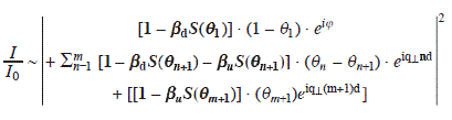
Following Shin and Aziz (2007), in the above equation the oscillations in the specular reflection have been modelled using Eq. 5.8 but importantly the specularly reflected intensity from each layer has been reduced by a factor [1 − βdS(θn + 1) − βuS(θn + 1)], which accounts for the step-edge scattering of the layer (θn +1) with step density S(θn + 1). The step reduces the specular reflection of the layer downwards of the step with an effective phenomenological constant βd and the reflection from the upward layer by βu, because diffuse scattering and shadowing effects occur at steps. This combination of the model (a) for interference in q⊥ and model (b) for diffuse scattering with a component in q|| can successfully explain oscillations at the anti-phase and in-phase conditions. Importantly though there are discrepancies to fully dynamic calculations that show an increase in the specularly reflected intensity at the in-phase condition for highly stepped surfaces (Korte and Maksym, 1997), where the above equation yields a lower reflectivity. This unexpected behaviour at the in-phase conditions already points to the fact that there is no fixed relationship between the stage in the growth cycle and a feature in the growth oscillation, and maxima of the intensity do not always occur for integer layer coverages. Due to multiple scattering effects, electron probes such as RHEED, while popular as fast and relatively simple techniques for qualitative monitoring of growth, are frequently more difficult to model quantitatively (Auciello and Krauss, 2001).
We note that in addition to elastic scattering techniques of course inelastic scattering and spectroscopy techniques using electrons are also applied in surface science experiments, such as electron energy loss spectroscopy (EELS) and Auger electron spectroscopy (AES).
5.4 Experimental case studies
In the case studies we give examples for a range of typical questions that can be answered by in-situ and real-time growth studies: which growth mode occurs, do roughness and island size scale with film thickness, is there transient strain, are there post-growth changes, and how do structure and optical properties correlate? Here we use examples from our own work and, for the purpose of coherence of the presentation, focus on growth of molecular thin films. In particular a series of experiments on diindenoperylene (DIP) on SiO2, will be insightful in regard to the questions above. Many concepts used here originally stem from MBE growth of atomic systems and are applicable for both molecular and atomic growth (Braun et al., 2003, Fleet et al., 2006, Woll et al, 1999).
We note that there are of course many other systems, for which we cannot even provide an exhaustive list of references. Besides the technically important field of MBE (see examples in this book and Farrow, 1995) there are also studies of ‘ablation’ and dissolution, which can be seen as ‘time-inverted’ growth and offers some interesting ways for comparison (Murty et al., 1998, Teng et al., 2001). For some of these, scattering is essentially the only way to monitor the process; in particular for dissolution/etching processes, the environment may be so harsh or hostile (extreme pH, ion sputtering and/or very high temperature) that SPM becomes almost impossible to apply since the tip would suffer in this environment.
We concentrate on examples of X-ray scattering and optical spectroscopy, but of course other real-time techniques discussed above have also been used to obtain information about growth modes and structural changes. The growth studies discussed in the following sections have been performed in a portable UHV growth chamber that is equipped with an X-ray window to allow for in-situ studies (Ritley et al., 2001), while, simultaneously with the X-ray measurements, DRS measurements can also be performed (Hosokai et al., 2010).
5.4.1 Transient strain during thin film growth
X-ray diffraction is a powerful technique to determine the crystal structure of thin films with high resolution, and for the molecule diindenoperylene (DIP) on SiO2 the thin-film unit cell dimensions have been determined by Kowarik et al. (2009a). Surface-sensitive GIXD is particularly suited to study thin films, and real-time measurements during DIP growth are sensitive to sub-monolayer coverages down to 0.1 ML. Figure 5.9 (a) shows the diffraction pattern for an early growth stage in the sub-ML regime where clear in-plane reflections are visible. Once the film has grown to a thickness of 5.3 ML the reflections get stronger and due to the out-of-plane periodicity also reflections along q± appear. Importantly, the diffraction image shows that the (110) and (120) in-plane reflections shift significantly during growth, while the (020) reflection shifts very little. This makes it possible to determine the changes of the in-plane lattice parameter during growth as shown in Fig. 5.9(b). The unit cell can be seen to expand by 3% along the a direction, while the b direction is nearly constant. Interestingly this change from the monolayer to a multilayer structure is complete, that is the originally compressed structure of the first monolayer is converted to the multilayer structure as can be seen by the disappearance of the corresponding reflection (Kowarik et al., 2006). Obviously, this transient effect would have been missed in post-growth studies.
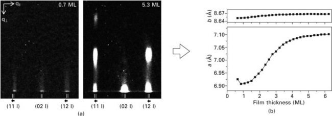
5.9 (a) Two snapshots of the GIXD pattern evolution during growth recorded with an area detector (Kowarik et at., 2009a). (b) Change of the in-plane lattice parameters during growth of the first monolayers.
5.4.2 Growth mode determination: X-ray anti-Bragg oscillations
During growth of DIP the X-ray reflectivity oscillates at the anti-Bragg condition as shown in Fig. 5.10. The period of oscillation between main maxima is 2 ML, but as a result of interference between substrate and DIP scattering (see Fig. 5.8) smaller maxima appear also when odd monolayers are completed. Some observations can be directly extracted from the experimental data. In particular, the maxima indicate when a ML is completed, which makes it possible to accurately determine the growth rate. The damping of the oscillations further indicates that the film gets rougher during growth. For a more detailed understanding, quantitative growth models have to be used for fitting the data, which for organic growth was to our knowledge first done in Krause et al. (2004b).
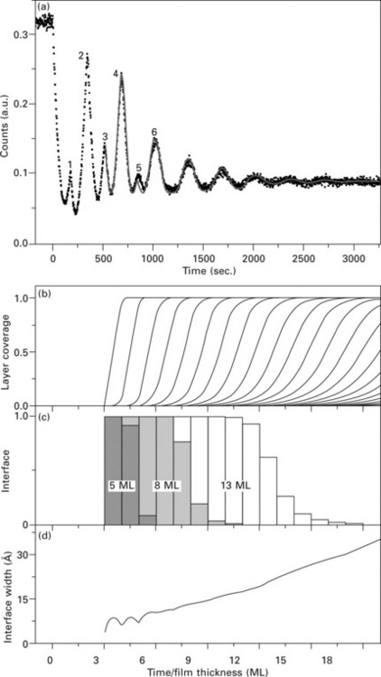
5.10 (a) X-ray anti-Bragg growth oscillation during DIP growth. (b) Individual layer coverages as function of film thickness. (c) Growth front for three thicknesses. (d) Roughness evolution during growth.
Fitting experimental scattering data is typically a two-step process: (i) growth theories are used to calculate the layer coverages θn; (ii) using this growth scenario, the experimental observables such as growth oscillations are simulated and the underlying parameter set is varied until a fit is achieved. We restrict the discussion to an intentionally simple and transparent growth model that can reproduce the experimental data reasonably well. For a description of more advanced growth models that are used to calculate the layer coverages, the reader is referred to Cohen et al. (1989), Barabási and Stanley (1995), Michely and Krug (2004) and Trofimov and Mokerov (2002).
In the diffusive growth model after Cohen et al. (1989) the rate for a jump from layer n + 1 to n is proportional to the uncovered fraction of layer n + 1 and the available space in layer n:
Here θn stands for the fractional coverage of the nth layer, t is the time to complete one monolayer, and kn is the effective rate for interlayer transport, that is the upward and downward rates are combined. Varying kn as a fit parameter for each layer, the anti-Bragg oscillations can be fitted from the fourth layer onwards. The first three layers have not been fitted because of the complications of transient strain, but both X-ray and AFM studies show that the first layers grow in a layer-by-layer fashion (Zhang et al., 2007).
The θn(t) resulting from a fit using Eq. 5.9 can be calculated as shown in Fig. 5.10(b). The interface of the DIP film for a given nominal coverage (e.g. 5, 8 and 13 ML) can be calculated from these θn(t) evaluated at the corresponding growth times and, in general, the film roughness can be extracted as a function of time/film thickness from the layer coverages. It is obvious that after ~ 5 ML of deposition the roughness starts to increase, which corresponds to the strong damping of the oscillations in this growth stage. This roughness increase is due to the significant decrease in downward (smoothing) interlayer current. In this simple model the reduction in the interlayer transport rate cannot be directly related to an increase in the Ehrlich–Schwöbel barrier, because the diffusion probability across a step also depends on the step-edge density which is not modelled in the simple rate equation. A recent AFM study on DIP has indeed shown, though, that the Ehrlich–Schwöbel barrier is layer dependent, and confirms the trend extracted from the model used here (Zhang et al., 2009).
5.4.3 Scaling laws: reflectivity and full q-range growth oscillations
Modern synchrotron sources make it possible to acquire not only a single point in reciprocal space but a wide q-range can be measured on a timescale of 10–100 seconds (essentially limited more by the moving speed of the X-ray diffractometer in angle dispersive experiments than by scattering intensities). Consequently, more information is acquired during the growth process, because many Fourier components of the real-space structure are sampled instead of only a single spatial frequency (Kowarik et al., 2009c). Figure 5.11(a) shows a typical dataset following the evolution of the specular reflectivity from the bare substrate up to a film thickness of 12 ML. This dataset can be analysed by either simulating growth oscillations (i.e., cuts through the 3D data f(q = const., d)) using the model described above, or by fitting the reflectivity curves at fixed points in time to directly extract information of the real-space structure (that is f(q, d = const.)).
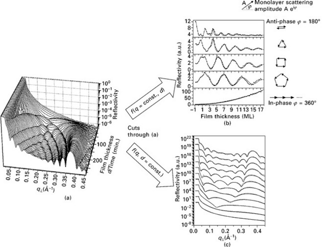
5.11 (a) Real-time reflectivity data for growth of DIP. (b) Cuts for fixed q values of q = 1/2, 2/3, 3/4, 4/5, 1/1 qBragg- (c) Cuts for fixed growth times/film thicknesses. Light grey lines are fits to the data according to the kinematic theory in (b) and Parratt theory in (c) (Kowarik et al., 2009c).
Figure 5.11 (b) shows growth oscillations at q values of ![]() (the anti-Bragg condition),
(the anti-Bragg condition), ![]() and
and ![]() The growth oscillations at q values larger than the anti-Bragg point oscillate with a slower period, and importantly also continue to oscillate after the anti-Bragg oscillations are completely damped out, that is information about later growth stages is only contained in the time evolution at larger q values in this case. The fits of growth oscillations can be performed using Eq. 5.7 which also naturally explains the increasing oscillation period on the time, i.e. thickness axis: at the anti-Bragg position complete destructive interference occurs after 2 ML are deposited resulting in a two ML oscillation period; at
The growth oscillations at q values larger than the anti-Bragg point oscillate with a slower period, and importantly also continue to oscillate after the anti-Bragg oscillations are completely damped out, that is information about later growth stages is only contained in the time evolution at larger q values in this case. The fits of growth oscillations can be performed using Eq. 5.7 which also naturally explains the increasing oscillation period on the time, i.e. thickness axis: at the anti-Bragg position complete destructive interference occurs after 2 ML are deposited resulting in a two ML oscillation period; at ![]() destructive inference occurs between three monolayers resulting in an oscillation period of 3 ML, and so on. Again, the rate equation model from Eq. 5.9 is combined with the kinematic scattering theory in Eq. 5.7. The result makes it possible to extract layer coverages, interlayer rate constants and evolution of surface roughness as illustrated by the example in Section 5.4.2.
destructive inference occurs between three monolayers resulting in an oscillation period of 3 ML, and so on. Again, the rate equation model from Eq. 5.9 is combined with the kinematic scattering theory in Eq. 5.7. The result makes it possible to extract layer coverages, interlayer rate constants and evolution of surface roughness as illustrated by the example in Section 5.4.2.
As a second approach, the Parratt algorithm (Parratt, 1954) can be applied to the same 3D dataset for describing the X-ray reflectivity as a function of q for a given time, i.e. thickness d. The Parratt fit can be restricted to q < π/dfilm if only the film roughness is of interest (Hinderhofer et al., 2010), but when including the modulation of the electron density due to the lattice periodicity, also the Bragg reflection can be fitted and the individual layer coverages can be extracted. For this approach no growth model has to be assumed and parameters such as surface roughness can be extracted directly. In Dürr et al. (2003) such Parratt fits have been applied to in-situ post-growth measurements to determine the roughening exponent ß from the thickness dependency of the film roughness (Fig. 5.12). The roughening exponent β was found to be 0.75, which remarkably is higher than the roughness exponent expected for random deposition. This behaviour is similar to other molecular systems and possibly related to the additional orientational and conformational degrees of freedom in molecular growth (Yim and Jones, 2006, Amassian et al., 2009, Dürr et al., 2003, Kowarik et al., 2007).
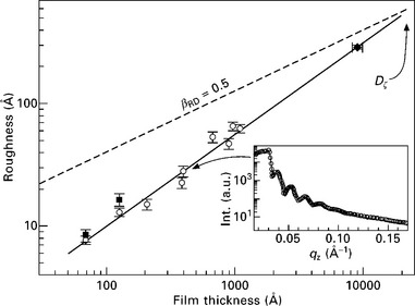
5.12 Scaling of the surface roughness with film thickness in DIP growth. Note that the data in this particular example were obtained post-growth (Dürr et al., 2003).
5.4.4 Post-deposition changes: dewetting of a molecular monolayer
Real-time techniques can not only be applied to growth itself, but also to re-arrangement and dewetting processes after the growth has stopped. This dewetting is technologically important as it can limit device stability in applications. For a monolayer of DIP the dewetting process has been followed using X-ray reflectivity as shown in Fig. 5.13. The specular reflectivity changes during evaporation of molecules onto a Si02 substrate at a temperature of 130 °C as expected for the formation of a closed monolayer.
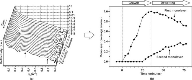
5.13 (a) X-ray reflectivity during growth and dewetting of DIP. (b) Coverages of the first and second DIP layer during growth and dewetting. The broken lines mark the opening and closing of the evaporation cell shutter (Kowarik et al., 2009b).
Using the Parratt formalism (Parratt, 1954) for fitting the X-ray reflectivity, the layer coverages of the first and second monolayers have been extracted as shown in Fig. 5.13(b). As expected for layer-by-layer growth, the coverage of the first monolayer nearly completes before nucleation of the second monolayer occurs. Shortly after the second layer nucleates, the flux of molecules is stopped. Closing the shutter after completion of the first monolayer, the X-ray reflectivity continues to change indicating a post-growth re-arrangement. In particular, the coverage of the second monolayer continues to rise while the coverage of the first monolayer shrinks. The rate of change is ~ (5.8 ± 1.0) × 10− 3 ML/min and the fact that the loss rate in the first monolayer and the gain rate in the second monolayer are equal shows that molecules are not desorbing, but rearranging. This example again demonstrates the usefulness of real-time observation. Ex-situ AFM measurements confirm the conclusions regarding the dewetting (Kowarik et al., 2009b), but the transient monolayer structure would be missed in post-growth measurements and of course the rate constant can only be determined in a time-resolved experiment.
5.4.5 Optical real-time studies
Following the optical properties and possible spectral changes in the growing film is also a powerful tool (Heinemeyer et al., 2010, Forker and Fritz, 2009). Of course, the optical properties are related to the structure, so that it is intriguing to study these simultaneously (Hosokai et al., 2010). Both optical properties and its interplay with film structure are highly relevant for organic devices, such as organic photovoltaic cells and organic light-emitting diodes.
Optical reflectance during thin film growth: DIP/SiO2
The different molecular environment at the interface compared to the bulk of a thin film, as well as structural changes also beyond the first monolayer, can give rise to an overall shift of the optical spectra, to a redistribution of oscillator strength or to the appearance of new transitions. Spectral changes as a function of thickness d are a very general effect. In the simplest approximation these decay as 1/d if they are purely interface-driven. For example, we can find the appearance of a new transition in DIP growth on SiO2 depending on film thickness (see Fig. 5.14 and Heinemeyer et al., 2010).
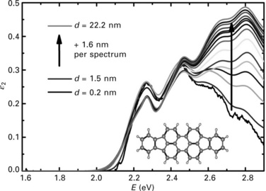
5.14 ε2(E) for a DIP film grown on glass. The thickness varies in steps of 1.6 nm from 0.2 nm to 22.2 nm. The modes at 2.25 eV (0-0), 2.48 eV (0-1) and 2.6 eV (0-2) are part of the vibronic progression, whereas the newly arising mode at 2.8 eV does not belong to it (Heinemeyer et al., 2010).
Simultaneous optical reflectance and GIXD during thin film growth: F16CuPc/SiO2
Simultaneous in-situ real-time measurements of X-ray reflectivity (XRR), grazing incidence X-ray diffraction (GIXD) and differential reflectance spectroscopy (DRS) were performed on per-fluorinated copper phthalocyanine (F16CuPc) thin films deposited on a SiO2/Si wafer (see Fig. 5.15(a) for the experimental setup, (b) for the real-time GIXD data taken at 303 K). Based on the X-ray data a structural transition within the first few layers of the film was established (De Oteyza et al., 2006).
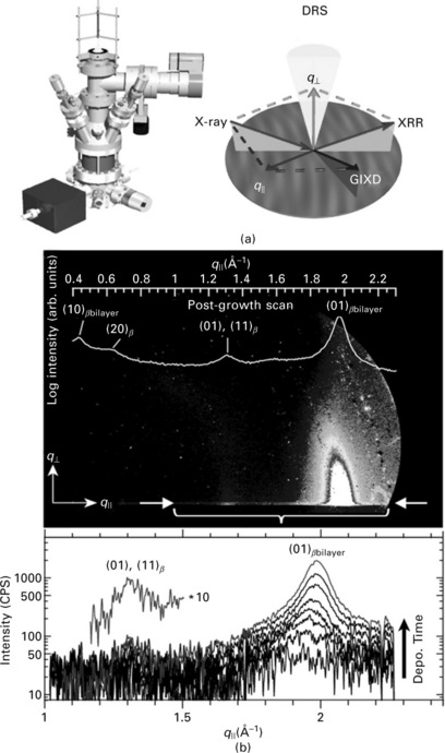
5.15 (a) Experimental setup. (b) Real-time GIXD data of F16CuPc deposited on SiO2 at 303 K. From Hosokai et al. (2010) with permission.
DRS spectra for selected film thicknesses with the corresponding numbers of molecular layers (ML) are shown in Fig. 5.16. Due to the structural transition of F16CuPc/SiO2 a significant variation of the spectra – especially below 2 ML – is observed. An absorption feature A and a broad shoulder B, which becomes dominant at 1 ML, are observed at 1.82 eV and 1.96 eV, respectively. In addition, a third feature C around 1.59 eV appears at 1 ML and becomes more intense with increasing film thickness.
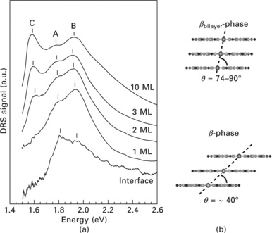
5.16 (a) Real-time DRS spectra of F16CuPc taken during deposition on SiO2 at 303 K. (b) Molecular arrangement for two F16CuPc phases. From Hosokai et al. (2010) with permission.
In the literature the absorption spectra of F16CuPc thin films have been discussed based on molecular exciton theory (Alonso et al., 2003). There, peak C is attributed to the β-phase of F16CuPc, that is characterized by ring-over-ring (eclipsed) π-orbital stackings and an inclined alignment of the transition dipoles (see Fig. 5.16(b)). It has also been noted (Schlettwein et al., 1999) that for F16ZnPc growth on glass substrates feature A is at similar energies as a peak found in solution spectra, suggesting that this feature could be related to an amorphous F16ZnPc phase in the film. With that information and on the basis of the XRR data the changes in the DRS spectra can be explained as follows.
Initially, the molecules prefer the flat-lying orientation and form an essentially amorphous film with spectra showing mainly feature A. After completion of the interface layer the molecules build up the bilayer structure reported by De Oteyza et al. (2006) with nearly parallel transition dipole moments, causing the observed increase of feature B. Finally, the thin film β-phase with the typical growth oscillations starts to nucleate. Above 2 ML the corresponding feature C appears in the spectrum. As is apparent from this example, a combination of several complementary real-time techniques greatly facilitates the understanding of a complicated growth mode.
5.5 Future trends
While ultra-fast experiments and atomic resolution individually can be achieved with comparative ease nowadays, the combination of fast time resolution, high spatial resolution, and surface sensitivity remains a challenge. Further, no single technique can span the wide time- and length scales that are relevant in growth processes so far.
Future progress will be driven by technological advances in monitoring techniques, allowing more and more of the above criteria to be combined. Interesting trends in X-ray scattering are photon counting pixel detectors that enable faster data acquisition, energy dispersive detectors that avoid motor scanning delays (Kowarik et al., 2007), and X-ray photon correlation spectroscopy (Seydel et al., 2003). New X-ray sources and in particular the X-ray laser will further enable ultra-fast X-ray scattering experiments with femtosecond time resolution. Also X-ray microscopy and tomography have been making significant progress in recent years and techniques such as interfacial X-ray microscopy (XRIM) is now established and can be applied to study growth, not only in vacuum but also in other complex environments (Fenter et al., 2006).
Optical techniques continue to benefit from increased availability of (solidstate) lasers in a wide wavelength range, and in particular (attosecond-)laser science and X-ray science increasingly merge as high harmonics of lasers reach the X-ray regime. This will enable much higher temporal resolution for studies of atomic structure during thin film growth in the future.
5.6 Sources of further information and advice
Further sources of information on real-time observation of growth can be found in a range of articles (Rost, 2007; Kowarik et al., 2009c; Rabe and Buchholz, 1991) and books (Auciello and Krauss, 2001; Braun, 1999). Growth modelling as the second central part of understanding the evolution of growth has been treated in a range of books on growth (Barabási and Stanley, 1995; Cohen et al, 1989; Krug, 1997, 2004; Markov, 2004; Michely and Krug, 2004; Pimpinelli and Villain, 1998; Shehu et al., 2010).
5.7 References
Alonso, M.I., Garriga, M., Osso, J.O., Schreiber, F., Barrena, E., Dosch, H. Strong optical anisotropies of F16CuPc thin films studied by spectroscopic ellipsometry. Journal of Chemical Physics. 2003; 119:6335–6340.
Amassian, A., Desai, T.V., Kowarik, S., Hong, S., Woll, A.R., Malliaras, G.G., Schreiber, F., Engstrom, J.R. Coverage dependent adsorption dynamics in hyperthermal organic thin film growth. The Journal of Chemical Physics. 2009; 130:124701.
Arwin, H., Aspnes, D.E. Unambiguous determination of thickness and dielectric function of thin-films by spectroscopic ellipsometry. Thin Solid Films. 1984; 113:101–113.
Aspnes, D.E., Quinn, W.E., Gregory, S. Application of ellipsometry to crystal-growth by organometallic molecular-beam epitaxy. Applied Physics Letters. 1990; 56:2569–2571.
Auciello, O., Krauss, A.R. In situ real time characterization of thin films. New York: Wiley; 2001.
Barabási, A.L., Stanley, H.E. Fractal Concepts in Surface Growth. Cambridge: Cambridge University Press; 1995.
Braun, W. Applied Rheed: Reflection High-energy Electron Diffraction During Crystal Growth. Berlin: Springer; 1999.
Braun, W., Jenichen, B., Kaganer, V.W., Shtukenberg, A.G., Däweritz, L., Ploog, K.H. Layer-by-layer growth of GaAs(001) studied by in situ synchrotron X-ray diffraction. Surface Science. 2003; 525:126–136.
Brune, H., Bromann, K., Röder, H., Kern, K., Jacobsen, J., Stoltze, P., Jacobsen, K., Norskov, J. Effect of strain on surface diffusion and nucleation. Physical Review B. 52, 1995. [R14380].
Cohen, P.I., Petrich, G.S., Pukite, P.R., Whaley, G.J., Arrott, A.S. Birth-death models of epitaxy: I. Diffraction oscillations from low index surfaces. Surface Science. 1989; 216:222–248.
Dale, D., Suzuki, Y., Brock, J.D. In situ x-ray reflectivity studies of dynamics and morphology during heteroepitaxial complex oxide thin film growth. Journal of Physics: Condensed Matter. 2008; 20:264008.
Dastoor, P.C., Allison, W. Geometric contrast mechanisms in helium atom scattering: the growth of the Fe/Cu(100) system. Physical Review B. 2003; 67:245403.
De Oteyza, D.G., Barrena, E., Ossó, J.O., Sellner, S., Dosch, H. Thickness-dependent structural transitions in fluorinated copper-phthalocyanine (F16CuPc) films. Journal of the American Chemical Society. 2006; 128:15052–15053.
Dürr, A.C., Schreiber, F., Ritley, K.A., Kruppa, V., Krug, J., Dosch, H., Struth, B. Rapid roughening in thin film growth of an organic semiconductor (diindenoperylene). Physical Review Letters. 2003; 90:016104.
Ehrlich, G., Hudda, F.G. Atomic view of surface self-diffusion: tungsten on tungsten. Journal of Chemical Physics. 1966; 44:1039–1049.
Ellis, J., Toennies, J.P., Witte, G. Helium atom scattering study of the frustrated translation mode of CO adsorbed on the Cu(001) surface. The Journal of Chemical Physics. 1995; 102:5059–5070.
Eres, G., Tischler, J., Yoon, M., Larson, B., Rouleau, C., Lowndes, D., Zschack, P. Time-resolved study of SrTiO3 homoepitaxial pulsed-laser deposition using surface x-ray diffraction. Applied Physics Letters. 2002; 80:3379–3381.
Farias, D., Rieder, K.-H. Atomic beam diffraction from solid surfaces. Reports on Progress in Physics. 1998; 61:1575–1664.
Farrow, R.F.C. Molecular Beam Epitaxy: Applications to Key Materials. Park Ridge, NJ: Noyes Publications; 1995.
Fendrich, M., Krug, J. Ehrlich–Schwoebel effect for organic molecules: direct calculation of the step-edge barrier using empirical potentials. Physical Review B (Condensed Matter and Materials Physics). 2007; 76:121302–121303.
Fenter, P.A. X-ray reflectivity as a probe of mineral-fluid interfaces: a user guide. Reviews in Mineralogy and Geochemistry. 2002; 49:149–221.
Fenter, P., Park, C., Zhang, Z., Wang, S. Observation of subnanometre-high surface topography with X-ray reflection phase-contrast microscopy. Nat Phys. 2006; 2:700–704.
Ferguson, J.D., Arikan, G., Dale, D.S., Woll, A.R., Brock, J.D. Measurements of surface diffusivity and coarsening during pulsed laser deposition. Physical Review Letters. 2009; 103:256103.
Fischer, B., Brune, H., Barth, J.V., Fricke, A., Kern, K. Nucleation kinetics on inhomogeneous substrates: Al/Au(111). Physical Review Letters. 1999; 82:1732–1735.
Fleet, A., Dale, D., Woll, A.R., Suzuki, Y., Brock, J.D. Multiple time scales in diffraction measurements of diffusive surface relaxation. Physical Review Letters. 2006; 96:055508.
Floreano, L., Cossaro, A., Gotter, R., Verdini, A., Bavdek, G., Evangelista, F., Ruocco, A., Morgante, A., Cvetko, D. Periodic arrays of Cu-phthalocyanine chains on Au(110). The Journal of Physical Chemistry C. 2008; 112:10794–10802.
Forker, R., Fritz, T. Optical differential reflectance spectroscopy of ultrathin epitaxial organic films. Physical Chemistry Chemical Physics. 2009; 11:2142–2155.
Forrest, S.R. Ultrathin organic films grown by organic molecular beam deposition and related techniques. Chemical Reviews. 1997; 97:1793–1896.
Frenken, J.W.M., Toennies, J.P., Wöll, C. Self-diffusion at a melting surface observed by He scattering. Physical Review Letters. 1988; 60:1727–1730.
Fuoss, P.H., Kisker, D.W., Lamelas, F.J., Stephenson, G.B., Imperatori, P., Brennan, S. Time-resolved x-ray scattering studies of layer-by-layer epitaxial growth. Physical Review Letters. 1992; 69:2791–2794.
Gerlach, A., Schreiber, F., Sellner, S., Dosch, H., Vartanyants, I.A., Cowie, B.C.C., Lee, T.-L., Zegenhagen, J. Adsorption-induced distortion of F16CuPc on Cu(111) and Ag(111): an X-ray standing wave study. Physical Review B. 2005; 71:205425.
Gerlach, A., Sellner, S., Schreiber, F., Koch, N., Zegenhagen, J. Substrate dependent bonding distances of PTCDA – a comparative X-ray standing wave study on Cu(111) and Ag(111). Physical Review B. 2007; 75:045401.
Haftel, M.I. Ehrlich–Schwoebel effect for vacancies: low-index faces of silver. Physical Review B. 2001; 64:125415.
Hartell, A.D., Tok, E.S., Zhang, J. The development of RAS and RHEED as in situ probes to monitor dopant segregation in GS-MBE on Si(001). Journal of Crystal Growth. 2001; 227:729–734.
Heinemeyer, U., Optical properties of organic semiconductor thin films: static spectra and real-time growth studies PhD thesis. Universität Tübingen, 2009.
Heinemeyer, U., Broch, K., Hinderhofer, A., Kytka, M., Scholz, R., Gerlach, A., Schreiber, F. Real-time changes in the optical spectrum of organic semiconducting films and their thickness regimes during growth. Physical Review Letters. 2010; 104:257401.
Hinch, B.J., Lock, A., Madden, H.H., Toennies, J.P., Witte, G. Helium-atom scattering investigation of facetting of the Al stepped (332) surface. Physical Review B. 1990; 42:1547.
Hinderhofer, A., Gerlach, A., Kowarik, S., Zontone, F., Krug, J., Schreiber, F. Smoothing and coherent structure formation in organic-organic heterostructure growth. EPL (Europhysics Letters). 2010; 91:56002.
Hlawacek, G., Puschnig, P., Frank, P., Winkler, A., Ambrosch-Draxl, C., Teichert, C. Characterization of step-edge barriers in organic thin-film growth. Science. 2008; 321:108–111.
Hofer, W.A., Foster, A.S., Shluger, A.L. Theories of scanning probe microscopes at the atomic scale. Reviews of Modern Physics. 2003; 75:1287–1331.
Hosokai, T., Gerlach, A., Hinderhofer, A., Frank, C., Ligorio, G., Heinemeyer, U., Vorobiev, A., Schreiber, F. Simultaneous in situ measurements of x-ray reflectivity and optical spectroscopy during organic semiconductor thin film growth. Applied Physics Letters. 2010; 97:063301.
Hyde, M.E., Jacobs, R., Compton, R.G. In situ AFM studies of metal deposition. The Journal of Physical Chemistry B. 2002; 106:11075–11080.
Jardine, A.P., Ellis, J., Allison, W. Quasi-elastic helium-atom scattering from surfaces: experiment and interpretation. Journal of Physics: Condensed Matter. 2002; 14:6173.
Kern, K., Niehus, H., Schatz, A., Zeppenfeld, P., Goerge, J., Comsa, G. Longrange spatial self-organization in the adsorbate-induced restructuring of surfaces: Cu{100}-(2 × 1)O. Physical Review Letters. 1991; 67:855–858.
Kneppe, M., Dorna, V., Kohstall, P., Kot, E., Köhler, U. A kinetic scanning tunneling microscopy study of iron silicide growth on Si(113). Surface Science. 2000; 454–456:802–806.
Koch, N., Gerlach, A., Duhm, S., Glowatzki, H., Heimel, G., Vollmer, A., Sakamoto, Y., Suzuki, T., Zegenhagen, J., Rabe, J.P., Schreiber, F. Adsorption-induced intramolecular dipole: correlating molecular conformation and interface electronic structure. Journal of the American Chemical Society. 2008; 130:7300–7304.
Korte, U., Maksym, P.A. Role of the step density in reflection high-energy electron diffraction: questioning the step density model. Physical Review Letters. 1997; 78:2381.
Kowarik, S., Gerlach, A., Sellner, S., Schreiber, F., Cavalcanti, L., Konovalov, O. Real-time observation of structural and orientational transitions during growth of organic thin films. Physical Review Letters. 2006; 96:125504.
Kowarik, S., Gerlach, A., Leitenberger, W., Hu, J., Witte, G., Wöll, C., Pietsch, U., Schreiber, F. Energy-dispersive X-ray reflectivity and GID for real-time growth studies of pentacene thin films. Thin Solid Films. 2007; 515:5606–5610.
Kowarik, S., Gerlach, A., Sellner, S., Cavalcanti, L., Konovalov, O., Schreiber, F. Real-time X-ray diffraction measurements of structural dynamics and polymorphism in diindenoperylene growth. Applied Physics A – Materials Science & Processing. 2009; 95:233–239.
Kowarik, S., Gerlach, A., Sellner, S., Cavalcanti, L., Schreiber, F. Dewetting of an organic semiconductor thin film observed in real-time. Advanced Engineering Materials. 2009; 11:291–294.
Kowarik, S., Gerlach, A., Skoda, M.W.A., Sellner, S., Schreiber, F. Real-time studies of thin film growth: measurement and analysis of X-ray growth oscillations beyond the anti-Bragg point. European Physical Journal – Special Topics. 2009; 167:11–18.
Krause, B., Durr, A.C., Schreiber, F., Dosch, H., Seeck, O.H. Late growth stages and post-growth diffusion in organic epitaxy: PTCDA on Ag(111). Surface Science. 2004; 572:385–395.
Krause, B., Schreiber, F., Dosch, H., Pimpinelli, A., Seeck, O.H. Temperature dependence of the 2D–3D transition in the growth of PTCDA on Ag(111): a real-time X-ray and kinetic Monte Carlo study. Europhysics Letters. 2004; 65:372–378.
Krug, J. Origins of scale invariance in growth processes. Advances in Physics. 1997; 46:139–282.
Krug, J. Power laws in surface physics: the deep, the shallow and the useful. Physica A. 2004; 340:647–655.
Krug, K., Stettner, J., Magnussen, O.M. In situ surface X-ray diffraction studies of homoepitaxial electrochemical growth on Au(100). Physical Review Letters. 2006; 96:246101–246104.
Lazzari, R., Renaud, G., Revenant, C., Jupille, J., Borensztein, Y. Adhesion of growing nanoparticles at a glance: surface differential reflectivity spectroscopy and grazing incidence small angle X-ray scattering. Physical Review B. 2009; 79:125428.
Lippmaa, M., Nakagawa, N., Kawasaki, M., Ohashi, S., Koinuma, H. Growth mode mapping of SrTiO3 epitaxy. Applied Physics Letters. 2000; 76:2439–2441.
Lüth, H. Solid Surfaces, Interfaces and Thin Films. Berlin: Springer-Verlag; 2001.
Markov, I.V. Crystal Growth for Beginners, 2nd ed. Hackensack, NJ: World Scientific Press; 2004.
McIntyre, J.D.E., Aspnes, D.E. Differential reflection spectroscopy of very thin surface films. Surface Science. 1971; 24:417–434.
McRae, E.G. Self-consistent multiple-scattering approach to the interpretation of low-energy electron diffraction. Surface Science. 1967; 8:14–34.
Mercurio, G., McNellis, E.R., Martin, I., Hagen, S., Leyssner, F., Soubatch, S., Meyer, J., Wolf, M., Tegeder, P., Tautz, F.S., Reuter, K. Structure and energetics of azobenzene on Ag(111): benchmarking semiempirical dispersion correction approaches. Physical Review Letters. 2010; 104:036102.
Meyer Zu Heringdorf, F.J., Reuter, M.C., Tromp, R.M. Growth dynamics of pentacene thin films. Nature. 2001; 412:517–520.
Michely, T., Krug, J. Islands, Mounds and Atoms: Patterns and Processes in Crystal Growth Far From Equilibrium. Heidelberg: Springer; 2004.
Murty, M.V.R., Curcic, T., Judy, A., Cooper, B.H., Woll, A.R., Brock, J.D., Kycia, S., Headrick, R.L. X-ray scattering study of the surface morphology of Au(111) during Ar + ion irradiation. Physical Review Letters. 1998; 80:4713–4716.
Oura, K., Lifshits, V.G., Saranin, A.A., Zotov, A.V., Katayama, M. Surface Science. Heidelberg: Springer; 2003.
Parratt, L.G. Surface studies of solids by total reflection of x-rays. Physical Review. 1954; 95:359–369.
Pimpinelli, A., Villain, J. Physics of Crystal Growth. Cambridge: Cambridge University Press; 1998.
Poelsema, B., Comsa, G., Scattering of Thermal Energy Atoms from Disordered Surfaces. Springer, Berlin/Heidelberg, 1989.
Poelsema, B., Becker, A.F., Rosenfeld, G., Kunkel, R., Nagel, N., Verheij, L.K., Comsa, G. On the shape of the in-phase TEAS oscillations during epitaxial growth of Pt(111). Surface Science. 1992; 272:269–275.
Rabe, J.P., Buchholz, S. Direct observation of molecular-structure and dynamics at the interface between a solid wall and an organic solution by scanning tunneling microscopy. Physical Review Letters. 1991; 66:2096–2099.
Ratsch, C., Scheffler, M. Density-functional theory calculations of hopping rates of surface diffusion. Physical Review B. 1998; 58:13163.
Ritley, K.A., Krause, B., Schreiber, F., Dosch, H. A portable ultrahigh vacuum organic molecular beam deposition system for in situ X-ray diffraction measurements. Review of Scientific Instruments. 2001; 72:1453–1457.
Rost, M.J. In situ real-time observation of thin film deposition: roughening, zeno effect, grain boundary crossing barrier, and steering. Physical Review Letters. 2007; 99:266101.
Rusponi, S., Boragno, C., Valbusa, U. Ripple structure on Ag(110) surface induced by ion sputtering. Physical Review Letters. 1997; 78:2795–2798.
Santoro, G., Franchini, A., Bortolani, V., Harten, U., Toennies, J.P., Wöll, C. Inelastic scattering of helium atoms from the phonons of the reconstructed Au(111) surface. Surface Science. 1987; 183:180–188.
Schlettwein, D., Graaf, H., Meyer, J.P., Oekermann, T., Jaeger, N.I. Molecular interactions in thin films of hexadecafluorophthalocyaninatozinc (F16PcZn) as compared to islands of N, N’-dimethylperylene-3,4,9,10-biscarboximide (MePTCDI). The Journal of Physical Chemistry B. 1999; 103:3078–3086.
Schreiber, F. Structure and growth of self-assembling monolayers. Progress in Surface Science. 2000; 65:151–257.
Schreiber, F. Organic molecular beam deposition: growth studies beyond the first monolayer. Physica Status Solidi A – Applied Research. 2004; 201:1037–1054.
Schreiber, F., Eberhardt, A., Leung, T.Y.B., Schwartz, P., Wetterer, S.M., Lavrich, D.J., Berman, L., Fenter, P., Eisenberger, P., Scoles, G. Adsorption mechanisms, structures, and growth regimes of an archetypal self-assembling system: decanethiol on Au.111. Physical Review B. 1998; 57:12476.
Schwoebel, R.L., Shipsey, E.J. Step motion on crystal surfaces. Journal of Applied Physics. 1966; 37:3682–3686.
Scoles, G., Bassi, D., Buck, U., Laine, D. Atomic and Molecular Beam Methods. Oxford: Oxford University Press; 1988.
Seidel, C., Poppensieker, J., Fuchs, H. Real-time monitoring of phase transitions of vacuum deposited organic films by molecular beam deposition LEED. Surface Science. 1998; 408:223–231.
Seydel, T., Madsen, A., Sprung, M., Tolan, M., Grubel, G., Press, W. Setup for in situ surface investigations of the liquid/glass transition with (coherent) x rays. Review of Scientific Instruments. 2003; 74:4033–4040.
Shehu, A., Quiroga, S.D., D’Angelo, P., Albonetti, C., Borgatti, F., Murgia, M., Scorzoni, A., Stoliar, P., Biscarini, F. Layered distribution of charge carriers in organic thin film transistors. Physical Review Letters. 2010; 104:246602.
Shin, B., Aziz, M.J. Modeling RHEED intensity oscillations in multilayer epitaxy: determination of the Ehrlich-Schwoebel barrier in Ge(001) homoepitaxy. Physical Review B. 2007; 76:165408.
Stadler, C., Hansen, S., Kroger, I., Kumpf, C., Umbach, E. Tuning intermolecular interaction in long-range-ordered submonolayer organic films. Nature Physics. 2009; 5:153–158.
Stephenson, G.B., Eastman, J.A., Thompson, C., Auciello, O., Thompson, L.J., Munkholm, A., Fini, P., Denbaars, S.P., Speck, J.S. Observation of growth modes during metal-organic chemical vapor deposition of GaN. Applied Physics Letters. 1999; 74:3326–3328.
Teng, H.H., Fenter, P., Cheng, L.W., Sturchio, N.C. Resolving orthoclase dissolution processes with atomic force microscopy and X-ray reflectivity. Geochimica et Cosmochimica Acta. 2001; 65:3459–3474.
Tischler, J.Z., Eres, G., Larson, B.C., Rouleau, C.M., Zschack, P., Lowndes, D.H. Nonequilibrium interlayer transport in pulsed laser deposition. Physical Review Letters. 2006; 96:226104.
Trofimov, V.I., Mokerov, V.G. Epitaxial growth kinetics in the presence of an Ehrlich-Schwoebel barrier: comparative analysis of different models. Materials Science and Engineering B. 2002; 89:420–425.
Van Der Vegt, H.A., Alvarez, J., Torrelles, X., Ferrer, S., Vlieg, E. Indium-induced layer-by-layer growth and suppression of twin formation in the homoepitaxial growth of Cu(111). Physical Review B. 1995; 52:17443–17448.
Venables, J. Introduction to Surface and Thin Film Processes. Cambridge: Cambridge University Press; 2000.
Venables, J.A., Spiller, G.D.T., Hanbucken, M. Nucleation and growth of thin films. Reports on Progress in Physics. 1984; 47:399–459.
Weightman, P., Martin, D.S., Cole, R.J., Farrell, T. Reflection anisotropy spectroscopy. Reports on Progress in Physics. 2005; 68:1251.
Weschke, E., SchuBler-Langeheine, C., Meier, R., Kaindl, G., Sutter, C., Abernathy, D., Grubel, G. q dependence of the growth-oscillation period of x-ray reflectivity in heteroepitaxy: Ho/W(110). Physical Review Letters. 1997; 79:3954–3957.
Williamson, M.J., Tromp, R.M., Vereecken, P.M., Hull, R., Ross, F.M. Dynamic microscopy of nanoscale cluster growth at the solid–liquid interface. Nat Mater. 2003; 2:532–536.
Witte, G., Wöll, C. External vibrations of hydrocarbons on Cu(100). The Journal of Chemical Physics. 1995; 103:5860–5863.
Witte, G., Wöll, C. Growth of aromatic molecules on solid substrates for applications in organic electronics. Journal of Materials Research. 2004; 19:1889–1916.
Woll, A.R., Headrick, R.L., Kycia, S., Brock, J.D. GaN nucleation and growth on sapphire(0001): incorporation and interlayer transport. Physical Review Letters. 1999; 83:4349–4352.
Xu, H., Yang, Y.-W., Engel, T. Quantification of defects in epitaxial metal film growth: a helium diffraction investigation of the Cu/W(110) system. Surface Science. 1991; 255:73–90.
Yamane, H., Gerlach, A., Duhm, S., Tanaka, Y., Hosokai, T., Mi, Y.Y., Zegenhagen, J., Koch, N., Seki, K., Schreiber, F. Site-specific geometric and electronic relaxations at organic-metal interfaces. Physical Review Letters. 2010; 105:046103.
Yim, S., Jones, T.S. Anomalous scaling behavior and Surface roughening in molecular thin-film deposition. Physical Review B. 2006; 73:161305.
Zangwill, A. Physics at Surfaces. Cambridge: Cambridge University Press; 1988.
Zhang, X.N., Barrena, E., De Oteyza, D.G., Dosch, H. Transition from layer-by-layer to rapid roughening in the growth of DIP on SiO2. Surface Science. 2007; 601:2420–2425.
Zhang, X., Barrena, E., Goswami, D., De Oteyza, D.G., Weis, C., Dosch, H. Evidence for a layer-dependent Ehrlich-Schwoebel barrier in organic thin film growth. Physical Review Letters. 2009; 103:136101.
Zheng, H., Smith, R.K., Jun, Y.-W., Kisielowski, C., Dahmen, U., Alivisatos, A.P. Observation of single colloidal platinum nanocrystal growth trajectories. Science. 2009; 324:1309–1312.