
Growth of graphene layers for thin films
Abstract:
Graphene has received considerable attention due to its fascinating physical properties such as quantum electronic transport, a tunable band gap, extremely high mobility, high elasticity and electromechanical modulation. This chapter describes the direct synthesis of large-scale graphene films using chemical vapour deposition on thin nickel layers, and presents two different methods of patterning the films and transferring them to arbitrary substrates. Furthermore, we detail the roll-to-roll production and wet chemical doping of predominantly monolayer 30-inch graphene films grown by chemical vapour deposition onto flexible copper substrates.
9.1 Introduction
In order to be used as nano-electronic devices, it is essential to grow graphene on a large scale. Among methods for graphene synthesis, graphene growth by chemical vapour deposition (CVD) on Ni and Cu has the advantage of growing graphene at large scale with uniform thickness. This chapter deals with graphene growth on Ni and Cu by CVD. First we describe large-scale graphene film synthesis using CVD on nickel layers, their pattern and their transfer to arbitrary substrates.1 In next section we detail the roll-to-roll production and wet chemical doping of predominantly monolayer 30-inch graphene films grown by CVD onto flexible copper substrates.2 Further, we detail how graphene electrodes were incorporated into a fully functional touchscreen panel device capable of withstanding high strain.
9.2 Large-scale pattern growth of graphene films for stretchable transparent electrodes
9.2.1 Direct synthesis of large-scale graphene films
Ni films were e-beam evaporated on SiO2/Si substrates, and thermally annealed. After exposing the Ni surface to a CH4, H2 and Ar mixture in atmospheric conditions, the system was rapidly cooled to room temperature. This fast cooling rate is critical in suppressing formation of multiple layers and for separating graphene layers efficiently from the substrate in the later process.3
A scanning electron microscope (SEM) image of graphene films on a thin nickel substrate shows clear contrast between areas with different numbers of graphene layers (Fig. 9.1a). Transmission electron microscope (TEM) images (Fig. 9.1b) show that the film consists mostly of less than a few layers of graphene. After transfer of the film to a silicon substrate with a 300 nm thick SiO2 layer, optical and confocal scanning Raman microscope images were made of the same area (Fig. 9.1c,d).4 The brightest area in Fig. 9.2(d) corresponds to monolayers, and the darkest area is composed of more than ten layers of graphene. Bilayer structures appear to predominate in both TEM and Raman images for this particular sample, which was prepared from 7 minutes of growth on a 300 nm thick nickel layer. It is found that the average number of graphene layers, the domain size and the substrate coverage can be controlled by changing the nickel thickness and growth process, thus providing a way of controlling the growth of graphene for different applications.

9.1 Various spectroscopic analyses of large-scale graphene films grown by CVD. (a) SEM images of as-grown graphene films on thin (300 nm) nickel layers and thick (1 mm) Ni foils (inset). (b) TEM images of graphene films of different thickness. (c) An optical microscope image of the graphene films transferred to a 300 nm thick silicon dioxide layer. The inset AFM image shows typical rippled structures. (d) A confocal scanning Raman image corresponding to (c). The number of layers is estimated from the intensities, shapes and positions of the G-band and 2D-band peaks. (e) Raman spectra (532 nm laser wavelength) obtained from the corresponding coloured spots in (c) and (d). a.u. = arbitrary units. (From Ref. [1].)
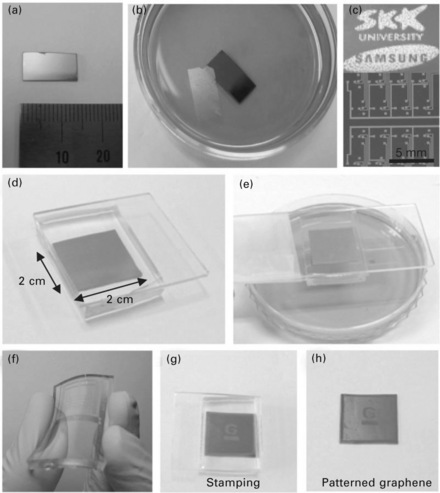
9.2 Transfer processes for large-scale graphene films. (a) A centimeter-scale graphene film grown on Ni(300 nm)/SiO2(300 nm)/Si substrate. (b) A floating graphene film after etching the nickel layers in 1 M FeCl3 aqueous solution. After the removal of the nickel layers, the floating graphene film can be transferred by direct contact with substrates. (c) Various shapes of graphene films can be synthesized on top of patterned nickel layers. (d, e) The dry-transfer method based on a PDMS stamp is useful in transferring the patterned graphene films. After attaching the PDMS substrate to the graphene (d), the underlying nickel layer is etched and removed using FeCl3 solution (e). (f) Graphene films on the PDMS substrates are transparent and flexible. (g, h) The PDMS stamp makes conformal contact with a silicon dioxide substrate. Peeling back the stamp (g) leaves the film on a SiO2 substrate (h). (From Ref. [1].).
Atomic force microscope (AFM) images often show the ripple structures caused by the difference between the thermal expansion coefficients of nickel and graphene (Fig. 9.1c).5 It is believed that these ripples make the graphene films more stable against mechanical stretching,6 making the films more expandable. Multilayer graphene films are preferable in terms of mechanical strength for supporting large-area film structures, whereas thinner graphene films have higher optical transparency. It is found that a ~300 nm thick nickel layer on a silicon wafer is the optimal substrate for the large-scale CVD growth that yields mechanically stable, transparent graphene films to be transferred and stretched after they are formed, and that thinner nickel layers with a shorter growth time yield predominantly mono- and bilayer graphene film for microelectronic device application.
9.2.2 Transfer processes for large-scale graphene films
The transfer of CVD-derived graphene films to non-specific substrates is enabled by FeCl3 etching of the underlying Ni film. Use of buffered oxide etchant (BOE) or hydrogen fluoride solution removes silicon dioxide layers, so the patterned graphene and the nickel layer float together on the solution surface. After transfer to a substrate, further reaction with BoE or hydrogen fluoride solution completely removes the remaining nickel layers.
A dry-transfer process has been developed for the graphene film using a soft substrate such as polydimethylsiloxane (PDMS) stamp.7 Here the PDMS stamp is first attached to the CVD-grown graphene film on the nickel substrate (Fig. 9.2d). The nickel substrate can be etched away using FeCl3 as described above, leaving the adhered graphene film on the PDMS substrate (Fig. 9.2e). By using the pre-patterned nickel substrate (Fig. 9.2c), we can transfer various sizes and shapes of graphene film to an arbitrary substrate. This dry-transfer process turns out to be very useful in making large-scale graphene electrodes and devices without additional lithography processes (Fig. 9.2f–h). Microscopically, these graphene films often show linear crack patterns with an angle of 60°C or 120°C, indicating a particular crystallographic edge with large crystalline domains. In addition, the Raman spectra measured for graphene films on nickel substrates show a strongly suppressed defect-related D-band peak. This D peak grows only slightly after the transfer process (Fig. 9.1e), indicating overall good quality of the resulting graphene film. Further optimization of the transfer process with substrate control makes possible transfer yields approaching 99%.
9.2.3 Optical and electrical properties of the graphene films
For the macroscopic transport electrode application, the optical and electrical properties of 1 × 1 cm2 graphene films were measured by ultraviolet-visible spectrometer and four-probe Van der Pauw methods, respectively (Fig. 9.3a,b). The transmittance is measured using an ultraviolet-visible spectrometer after transferring the floating graphene film to a quartz plate (Fig. 9.3a). In the visible range, the transmittance of the film grown on a 300 nm thick nickel layer for 7 minutes is ~80%, a value similar to those found for previously studied assembled films.8,9 Because the transmittance of the graphene layer is ~2.3%,10 this transmittance can be increased to ~93% by further reducing the growth time and nickel thickness, resulting in a thinner graphene film. Ultraviolet/ozone etching is also useful in controlling the transmittance under ambient conditions (Fig. 9.4a, upper inset). Indium electrodes were deposited on each corner of the square (Fig. 9.3a, lower inset) to minimize contact resistance. The minimum sheet resistance is ~280 Ω per square, which is ~30 times smaller than the lowest sheet resistance measured on assembled films.8,9 The values of sheet resistance increase with the ultraviolet/ozone treatment time, in accordance with the decreasing number of graphene layers (Fig. 9.3a)
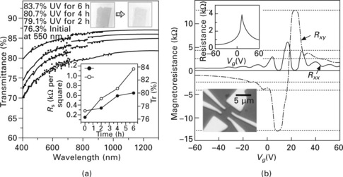
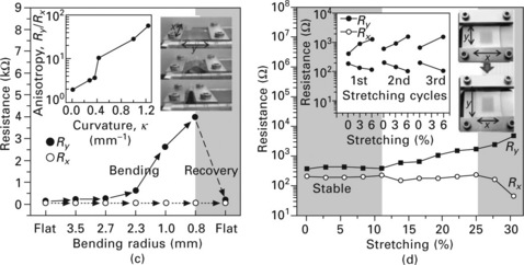
9.3 Optical and electrical properties of graphene films. (a) Transmittance of the graphene films on a quartz plate. The discontinuities in the absorption curves arise from the different sensitivities of the switching detectors. The upper inset shows the ultraviolet (UV)-induced thinning and the consequent enhancement of transparency. The lower inset shows the changes in transmittance, Tr, and sheet resistance, Rs, as functions of ultraviolet illumination time. (b) Electrical properties of monolayer graphene devices showing half-integer quantum Hall effect and high electron mobility. The upper inset shows a four-probe electrical resistance measurement on a monolayer graphene Hall bar device (lower inset) at 1.6 K. A gate voltage, Vg, is applied to the silicon substrate to control the charge density in the graphene sample. The main panel shows longitudinal (Rxx) and transverse (Rxy) magnetoresistances measured in this device for a magnetic field B = 8.8 T. The monolayer graphene quantum Hall effect is clearly observed, showing the plateaux with filling factor v = 2 at Rxy = (2e2/h)− 1 and zeros in Rxx. (Here e is the elementary charge and h is Plank’s constant.) Quantum Hall plateaux (horizontal dashed lines) are developing for higher filling factors. (c) Variation in resistance of a graphene film transferred to a ~0.3 mm thick PDMS/PET substrate for different distances between holding stages (that is, for different radii). The left inset shows the anisotropy in four-probe resistance, measured as the ratio Ry/Rx, of the resistances parallel and perpendicular to the binding direction, y. The right inset shows the bending process. (d) Resistance of a graphene film transferred to a PDMS substrate isotropically stretched by ~12%. The left inset shows the case in which the graphene film is transferred to an unstretched PDMS substrate. The right inset shows the movement of holding stages and the consequent change in shape of the graphene film. (From Ref. [1].)

9.4 Photographs of the roll-based production of graphene films. (a) Copper foil wrapping around 7.5 inch quartz tube to be inserted into an 8 inch quartz reactor. The lower image shows the stage in which the copper foil reacts with CH4 and H2 gases at high temperatures. (b) Roll-to-roll transfer of graphene films from a thermal release tape to a PET film at 120°C. (c) A transparent ultra-large-area graphene film transferred on a 35 inch PET sheet. (d) Screen printing process of silver paste electrodes on graphene/PET film. The inset shows 3.1 inch graphene/PET panels patterned with silver electrodes before assembly. (e) An assembled graphene/PET touch panel showing outstanding flexibility. (f) A graphene-based touchscreen panel connected to a computer with control software. (From Ref. [2].)
For microelectronic application, the mobility of the graphene film is critical. To measure the intrinsic mobility of a single-domain graphene sample, the graphene samples are transferred from a PDMS stamp to a degenerate doped silicon wafer with a 300 nm deep thermally grown oxide layer. Monolayer graphene samples were readily located on the substrate from optical contrast10 and their identification was subsequently confirmed by Raman spectroscopy.4 Electron beam lithography was used to make multi-terminal devices (Fig. 9.3b, lower inset). Notably, the multi-terminal electrical measurements showed that the electron mobility is ~3750 cm2 V− 1 s− 1 at a carrier density of ~5 × 1012 cm− 2 (Fig. 9.3b). For a high magnetic field of 8.8T, the half-integer quantum Hall effect (Fig. 9.3b) is observed, indicating that the quality of CVD-grown graphene is comparable to that of mechanically cleaved graphene.
In addition to the good optical and electrical properties, the graphene film has excellent mechanical properties when used to make flexible and stretchable electrodes (Fig. 9.3c,d)7 The foldability of the graphene films, transferred to a polyethylene terephthalate (PET) substrate (thickness, ~100 μm) coated with a thin PDMS layer (thickness, ~200 μm; Fig. 9.3c), is evaluated by measuring resistances with respect to bending radii. The resistances show little variation up to the bending radius 2.3 mm (approximate tensile strain of 6.5%), and are perfectly recovered after unbending. Notably, the original resistance can be restored even for the bending radius of 0.8 mm (approximate tensile strain of 18.7%), exhibiting extreme mechanical stability in comparison with conventional materials used in flexible electronics.11
The resistance of graphene films transferred to pre-strained and unstrained PDMS substrates was measured with respect to uniaxial tensile strain ranging from 0 to 30% (Fig. 9.3d). Similar to the results in the folding experiment, the transferred film on the unstrained substrate recovers its original resistance after stretching by ~6% (Fig. 9.3d, left inset). However, further stretching often results in mechanical failure. Thus, it was tried transferring the film to pre-strained substrates12 to enhance the electromechanical stabilities by creating ripples similar to those observed in the growth process (Fig 9.1c, inset). The graphene transferred to a longitudinally strained PDMS substrate does not show much enhancement, owing to the transverse strain induced by Poisson’s effect.13 To prevent this problem, the PDMS substrate was isotopically stretched by ~12% before transferring the film to it (Fig. 9.3d). Surprisingly, both longitudinal and transverse resistance (Ry and Rx) appear stable up to ~11% stretching and show only one order of magnitude change at ~25% stretching. It is supposed that further uniaxial stretching can change the electronic band structure of graphene, leading to the modulation of sheet resistance. These electrochemical properties thus show graphene films to be not only the strongest14 but also the most flexible and stretchable conducting transparent materials so far measured.10
9.3 Roll-to-roll production of 30-inch graphene films for transparent electrodes
9.3.1 Synthesis of 30-inch graphene films and roll-to-roll transfer of graphene films
Figures 9.4a–c present photographs of the roll-based synthesis and transfer process. An 8-inch-wide tubular quartz reactor (Fig. 9.4a) is used in the CVD system, allowing a monolayer graphene film to be synthesized on a roll of copper foil with dimensions as large as 30 inches in the diagonal direction (Fig. 9.4c). A temperature gradient usually exists that depends on the radial position inside the tubular reactor. In our preliminary work, this sometimes resulted in inhomogeneous growth of the graphene on the copper foils. To solve this problem, a ~7.5-inch quartz tube wrapped with a copper foil was inserted and suspended inside the 8-inch quartz tube. In this way, the radial inhomogeneity in the reaction temperature could be minimized. In the first step of synthesis, the roll of copper foil is inserted into a tubular quartz tube and then heated to 1000°C with flowing 8 standard cubic centimetres per minute) (sccm) H2 at 90 mtorr. After reaching 1000°C, the sample is annealed for 30 minutes without changing the flow rate or pressure. The copper foils are heat-treated to increase the grain size from a few micrometers to ~100 μm, as we have found that the copper foils with larger grain size yield higher-quality graphene films, as suggested by Li and colleagues.15 The gas mixture of CH4 and H2 is then flowed at 460 mtorr at rates of 24 and 8 sccm for 30 minutes, respectively. Finally, the sample is rapidly cooled to room temperature (~10°C s− 1) with flowing H2 under a pressure of 90 mtorr.
After growth, the graphene film grown on copper foil is attached to a thermal release tape by applying soft pressure (~0.2 MPa) between two rollers. After etching the copper foil in a plastic bath filled with copper etchant, the transferred graphene film on the tape is rinsed with deionized water to remove residual etchant, and is ready to be transferred to any kind of flat or curved surface on demand. The graphene film on the thermal release tape is inserted between the rollers together with a target substrate (Fig. 9.4b). By repeating these steps on the same substrate, multilayered graphene films can be prepared that exhibit enhanced electrical and optical properties, as demonstrated by Li and colleagues using wet-transfer methods at the centimeter scale.16 Figure 9.4(c) shows the 30-inch multilayer graphene film transferred to a roll of 188 mm thick polyethylene terephthalate (PET) substrate. Figure 9.4(d) shows a screen-printing process used to fabricate four-wire touchscreen panels17 based on graphene/PET transparent conducting films. After printing electrodes and dot spacers, the upper and lower panels are carefully assembled and connected to a controller installed in a laptop computer (Figs 9.4e and f), which shows extraordinary flexibility. The scalability and processability of CVD graphene and the roll-to-roll methods presented here are expected to enable the continuous production of graphene-based electronic devices at large scales.
The graphene films seem to be predominantly composed of monolayers when analysed using Raman spectra (Fig. 9.5a). However, atomic force microscope (AFM) and transmission electron microscope (TEM) images often show bilayer and multilayer islands. As the graphene layers are transferred one after another,16 the intensities of the G- and 2D-band peaks increase together, but their ratios do not change significantly. This is because the hexagonal lattices of the upper and lower layers are randomly oriented, unlike the graphite, so the original properties of each monolayer remain unchanged, even after stacking into multilayers;18,19 this is clearly different from the case of multilayer graphene exfoliated from graphite crystals.4 The randomly stacked layers behave independently without significant change in the electronic band structures, and the overall conductivity of the graphene films appears to be proportional to the number of stacked layers.16 The optical transmittance is usually reduced by ~2.2–2.3% for an additional transfer, implying that the average thickness is approximately a monolayer (Fig. 9.5b).10
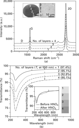

9.5 Optical characterizations of the graphene films prepared using layer-by-layer transfer on SiO2/silicon and PET substrates. (a) Raman spectra of graphene films with different numbers of stacked layers. The left inset shows a photograph of transferred graphene layers on a 4 inch SiO2 (300 nm)/silicon wafer. The right inset is a typical optical microscope image of the monolayer graphene, showing > 95% monolayer coverage. A PMMA-assisted transfer method is used for this sample. (b) UV-vis spectra of roll-to-roll layer-by-layer transferred graphene films on quartz substrates. The inset shows the UV spectra of graphene films with and without HNO3 doping. The right inset shows optical images for the corresponding number of transferred layers (1 × 1 cm2). The contrast is enhanced for clarity. (c) Raman spectra of HNO3-doped graphene films, showing ~18 cm− 1 blueshift both for G and 2D peaks. D-band peaks are not observed before or after doping, indicating that HNO3 treatment is not destructive to the chemical bonds of graphene. (d) XPS peaks of monolayer graphene films transferred on SiO2/Si substrates, showing typical redshift and broadening of carbon 1s peaks (C1s) caused by p-doping. The inset shows work function changes (ΔΦ) with respect to doping time (lower x-axis), measured by UPS. (From Ref. [2].)
The unique electronic band structure of graphene allows modulation of the charge carrier concentrations, depending on an electric field induced by gate bias20 or chemical doping,21 resulting in enhancement of sheet resistance. We tried various types of chemical doping methods, and found that nitric acid is very effective for p-doping of graphene films. Figure 9.5(c) shows Raman spectra of the graphene films before and after doping with 63 wt% HNO3 for 5 minutes. The large peak shift (Δu= 18 cm–1) indicates that the graphene film is strongly p-doped. The shifted G peak is often split near the randomly stacked bilayer islands, as shown in Fig. 9.5(c). We hypothesize that the lower graphene layer, which is screened by top layers, experiences a reduced doping effect, leading to G-band splitting. In X-ray photoelectron spectra (XPS), the C 1s peaks corresponding to sp2 and sp3 hybridized states are shifted to lower energy, similar to the case for p-doped carbon nanotubes.21 However, multilayer stacking results in blueshifted C1s peaks. We suppose that weak chemical bonding such as π-π stacking interaction causes descreening of nucleus charge, leading to an overall increase in core electron binding energies. We also find that the work functions of graphene films as estimated by UV photoelectron spectroscopy (UPS) are blueshifted by ~130 meV with increasing doping time (Fig. 9.5d, inset). The multiple stacking also changes the work functions (Fig. 9.5d, inset) which could be very important in controlling the efficiency of photovoltaic22 or light-emitting devices based on graphene transparent electrodes.23
9.3.2 Optical and electrical properties of graphene films
The electrical properties of graphene films formed using layer-by-layer staking methods were also investigated. Usually, the sheet resistance of graphene film with 97.4% transmittance is as low as ~125 Ω/sq (Fig. 9.6a) when it is transferred by a soluble polymer support such as polymethyl methacrylate (PMMA).16,24,25 The transferrable size achievable using a wet transfer method is limited to less than a few inches of wafer because of the weak mechanical strength of spin-coated PMMA layers. However, the scale of roll-to-roll dry transfer assisted by a thermal release tape is in principle unlimited. In the process of roll-to-roll dry transfer, the first layer sometimes shows approximately two to three times larger sheet resistance than that of the PMMA-assisted wet transfer method. As the number of layers increases, the resistance drops faster compared to the wet transfer method (Fig. 9.6a). We postulate that the adhesion of the first layer with the substrate is not strong enough for complete separation of the graphene films from the thermal release tape. As a result, there can be mechanical damage on the graphene films, leading to an increase in the overall sheet resistance. Because additional layers are not directly affected by the adhesion with the substrate surface, the sheet resistance of multilayers prepared by the roll- to-roll method does not differ much from that for the wet transfer case. The p-doping with HNO3 clearly enhances the electrical properties of graphene films, and is more effective in roll-to-roll processes. The sheet resistance of the p-doped four-layer graphene film with ~90% optical transmittance is as low as ~30 Ω/sq, which is superior to common transparent electrodes such as indium tin oxide (ITO) and carbon-nanotube films (Fig. 9.6b).26


9.6 Electrical characterization of layer-by-layer transferred and HNO3-doped graphene films. (a) Sheet resistances of transferred graphene films using roll-to-roll (R2R) dry transfer method combined with thermal release tapes and a PMMA-assisted wet transfer method. (b) Comparison of sheet resistance from this research and transmittance plots taken from other references. The dashed arrows indicate the expected sheet resistances at lower transmittance. (c) Electrical properties of a monolayer graphene Hall bar device in vacuum. Four-probe resistivity (left inset) is measured as a function of gate voltage in the monolayer graphene Hall bar shown in the right inset at room temperature (solid curve) and T = 6 K (dashed curve). The QHE effect at T = 6 K and B = 9 T is measured in the same device. The longitudinal resistivity ρxx and Hall conductivity σxy are plotted as a function of gate voltage. The sequence of the first three half-integer plateaux corresponding to υ = 2, 6 and 10, typical for single-layer graphene, are clearly seen. The Hall effect mobility of this device is μHall = 7350 cm− 2 V− 1 s− 1 at 6 K (~5100 cm− 2 V− 1 s− 1 at 295 K). Scale bar (inset), 3 μm. (d) Electromechanical properties of graphene-based touchscreen devices compared with ITO/PET electrodes under tensile strain. The inset shows the resistance changes with compressive and tensile strain applied to the upper and lower graphene/PET panels, respectively. (From Ref. [2].)
Standard electron-beam lithography has been used to fabricate graphene Hall bars on conventional 300 nm SiO2/Si substrates (Fig. 9.6c). The left inset of Fig. 9.6c shows the four-terminal resistance of such samples as a function of backgate voltage (Vbg) at both room temperature (solid curve) and at a low temperature (T = 6K) and zero magnetic field. We observe the graphene specific gate bias dependence of the resistance with a sharp Dirac peak and an effective Hall mobility of 7350 cm2 V–1 s–1 at low temperatures. This allows the observation of the quantum Hall effect (QHE)27 at 6K and a magnetic field of B = 9T (Fig. 9.6c, right). The fingerprint of single-layer graphene, the half-integer quantum Hall effect, is observed with plateaux at filling factors of u = 2,6 and 10 at Rxy = 1/2, 1/6 and 1/10 (h2/e2), respectively. Although the sequence of the plateaux remains for both the electron side and the hole side, there is a slight deviation from the fully quantized values on the hole side.
Finally, the electromechanical properties of graphene/PET touchscreen panels were tested (Fig. 9.6d). Unlike an ITO-based touch panel, which easily breaks under ~2–3% strain, the graphene-based panel resists up to 6% strain; this is limited not by the graphene itself, but by the printed silver electrodes (Fig. 9.6d).28
9.4 Conclusions
In conclusion, we showed a method for graphene growth on nickel and copper layers using chemical vapour deposition and further described a method to transfer graphene films to stretchable substrates. This will lead to numerous applications including use in large-scale flexible, stretchable, foldable transparent electronics. In addition, given the scalability and processability of roll-to-roll and CVD methods and the flexibility and conductivity of graphene films, we anticipate that the commercial production of large-scale transparent electrodes, replacing ITO, will be realized in the near future.
9.5 References
1. Hong, B.H., et al. Large-scale pattern growth of graphene films for stretchable transparent electrodes. Nature. 2009; 457:706–710.
2. Hong, B.H., et al. Roll-to-roll production of 30-inch graphene films for transparent electrodes. Nature Nanotech. 2010; 5:574–578.
3. Yu, Q., et al. Graphene segregated on Ni surfaces and transferred to insulators. Appl. Phys. Lett. 93, 2008. [113103].
4. Ferrari, A.C., et al, Raman spectrum of graphene and graphene layers. Phys. Rev. Lett, 2006. [187401].
5. Obraztsov, A.N., Obraztsova, E.A., Tyurnina, A.V., Zolotukhin, A.A. Chemical vapor deposition of thin graphite films of nanometer thickness. Carbon. 2007; 45:2017–2021.
6. Khang, D.-Y., et al. Individual aligned single-wall carbon nanotubes on elastomeric substrates. Nano Lett. 2008; 8:124–130.
7. Yang, P., et al. Mirrorless lasing from mesostructured waveguides patterned by soft lithography. Science. 2000; 287:465–467.
8. Li, X., et al. Highly conducting graphene sheets and Langmuir–Blodgett films. Nature Nanotechnol. 2008; 3:538–542.
9. Eda, G., Fanchini, G., Chhowalla, M. Large-area ultrathin films of reduced graphene oxide as a transparent and flexible electronic material. Nature Nanotechnol. 2008; 3:270–274.
10. Nair, R.R., et al. Fine structure constant defines visual transparency of graphene. Science. 2008; 320:1308.
11. Lewis, J. Material challenge for flexible organic devices. Mater. Today. 2006; 9:38–45.
12. Sun, Y., Choi, W.M., Jiang, H., Huang, Y.Y., Rogers, J.A. Controlled buckling of semiconductor nanoribbons for strechable electronics. Nature Nanotechnol.. 2006; 1:201–207.
13. Khang, D.-Y., Jiang, H., Huang, Y., Rogers, J.A. A stretchable form of single crystal silicon for high-performance electronics on rubber substrates. Science. 2006; 311:208–212.
14. Lee, C., Wei, X., Kysar, J.W., Hone, J. Measurement of the elastic properties and intrinsic strength of monolayer graphene. Science. 2008; 321:385–388.
15. Li, X., et al. Large-area synthesis of high-quality and uniform graphene films on copper foils. Science. 2009; 324:1312–1314.
16. Li, X., et al. Transfer of large-area graphene films for high-performance transparent conductive electrodes. Nano Lett. 2009; 9:4359–4363.
17. Hecht, D.S., et al. Carbon nanotube film on plastic as transparent electrode for resistive touch screens. J. Soc. Inf. Display. 2009; 17:941–946.
18. Hass, J., et al. Why multilayer graphene on 4H-SiC(000-1) behaves like a single sheet of graphene. Phys. Rev. Lett. 100, 2008. [125504].
19. Sprinkle, M., et al. First direct observation of a nearly ideal graphene band structure. Phys. Rev. Lett. 103, 2009. [226803].
20. Das, A., et al. Monitoring dopants by Raman scattering in an electrochemically top-gated graphene transistor. Nature Nanotech. 2008; 3:210–215.
21. Geng, H.-Z., et al. Effect of acid treatment on carbon nanotube-based flexible transparent conducting films. J. Am. Chem. Soc. 2007; 129:7758–7759.
22. Schrivera, M., Reganb, W., Losterb, M., Zettl, A. Carbon nanostructure-aSi:H photovoltaic cells with high open-circuit voltage fabricated without dopants. Solid State Commun.. 2010; 150:561–563.
23. Wu, J., et al. Organic light-emitting diodes on solution-processed metal nanowire mesh transparent electrodes. ACS Nano. 2010; 4:43–48.
24. Reina, A., et al. Large area, few-layer graphene films on arbitrary substrates by chemical vapor deposition. Nano Lett. 2009; 9:30–35.
25. Cai, W.W., et al. Large area few-layer graphene/graphite films as transparent thin conducting electrodes. Appl. Phys. Lett.. 95, 2009. [123115].
26. Lee, J.-Y., Connor, S.T., Cui, Y., Peumans, P. Solution-processed metal nanowire mesh transparent electrodes. Nano Lett. 2008; 8:689–692.
27. Cao, H.L., et al. Electronic transport in chemical vapor deposited graphene synthesized on Cu: Quantum Hall effect and weak localization. Appl. Phys. Lett. 96, 2010. [122106].
28. Cairns, D.R., et al. Strain-dependent electrical resistance of tin-doped indium oxide on polymer substrates. Appl. Phys. Lett. 2000; 76:1425–1427.