
Silicon nanostructured films grown on templated surfaces by oblique angle deposition
Abstract:
We observed that the deposition of silicon (Si) nanostructured thin films on a patterned substrate with oblique angle incidence flux gives rise to a phenomenon referred to as ‘fan-out’ growth, which entails the overgrowth of the structures along the direction perpendicular to the incident deposition flux. We concluded in our Monte Carlo simulations that the side-sticking of incoming particles to the previously deposited particles is the cause of ‘fan-out’ growth. We have designed two methods to overcome fan-out growth: ‘two-phase’ rotation and ‘swing’ rotation. By these methods, uniform slanted Si nanorods and square nanosprings were fabricated.
6.1 Introduction
The morphological evolution and pattern formation in growing surfaces have been the subject of intense study using a framework of statistical mechanics in the past decades (Barabasi and Stanley, 1995; Meakin, 1998; Marsili et al., 1996). Several theoretical growth models have been proposed to describe the deposition processes and scaling behaviors of a growing surface with the atoms depositing from an orthogonal flux on a smooth substrate (Barabasi and Stanley, 1995; Kardar et al., 1989; Tong and Williams, 1994). On the other hand, there has been little effort made to understand the process of atoms striking the surface from non-normal directions (Meakin and Krug, 1992; Barabasi and Stanley, 1995). This process, referred to as oblique angle deposition, can result in a porous thin film whose porosity greatly depends on the incident angle of the atoms.
In 1995, Robbie and Brett systematically studied the oblique angle deposition with substrate rotation method, which they called ‘glancing angle deposition’ (GLAD), at an incident angle close to 90° with respect to the substrate normal in experiments (Robbie et al., 1995a,b). The substrate rotation was driven through a stepper motor and a computer programmed to control the motion of the motor. Since then, this technique has been demonstrated as a powerful tool to create complex nanostructured thin films (Robbie et al., 1996; Hawkeye and Brett, 2007). Figure 6.1(a) shows a common system used for oblique angle deposition with the freedom of substrate rotation through a stepper motor. A large distance between the substrate and source is necessary to grow high quality structured thin film in oblique angle deposition. For some systems, a collimator or a nozzle can be used to minimize the angular spread of the deposition flux. The source materials can be evaporated at sufficiently low base pressures by methods such as thermal evaporation, electron-beam evaporation, pulsed laser ablation, and sputtering. Either single elements or compounds can be deposited in oblique angle deposition with a suitable evaporation method. As the incident atoms approaching the surface at an incident angle θ, as shown in Fig. 6.1(a), they will deposit on the extruding part of the surface. The lower parts of the surface are shadowed by the neighboring structures. This is called the ‘global shadowing effect’, as illustrated in the inset of Fig. 6.1. After landing on the surface, the atoms may diffuse across the surface to an energetically favorable site. As discussed above, the substrates can be placed in the chamber and locked in a fixed position, or can be rotated in a designed motion pattern. For both cases, a columnar thin film is the result of the competition between shadowing effect and surface diffusion. The difference is that tilted columns will grow if the substrate is fixed in one position, while vertical columns will grow if the substrate is rotated with sufficient speed, as shown in Fig. 6.1(b).

6.1 (a) Schematic of a common oblique angle deposition setup. The substrate can be rotated by a stepper motor. The shadowing effect is depicted in the inset. (b) Nanorod structures resulting from shadowing effect in oblique angle deposition. In the fixed substrate case, tilted nanorods will grow; in the rotating substrate case, vertical nanorods can be deposited.
In the case of no substrate rotation in oblique angle deposition, the columns tend to incline toward the incident flux to a tilt angle β, which is measured from the substrate normal. There is an empirical rule known as the ‘tangent rule’ describing the relationship of β and θ as (Nieuwenheuzen and Haanstra, 1966; Leamy et al., 1980):
The origin of the tangent rule result is generally believed to be the limited surface diffusion and the shadowing of atoms on the surface caused by the finite size of the atoms (Ablemann and Lodder, 1997). This tangent rule is not universal, however, because the tilt angles also depend on the deposition conditions and the material properties (Nakhodkin and Shaldervan, 1972; Hashimoto et al., 1982; Geszti et al., 1986). Even for the same material, the tangent rule will not hold for all incident angles. For larger incident angles (generally θ > 60°), another empirical rule called the ‘cosine rule’ may give better fitting of the experimental data (Trait et al., 1993; Tang et al., 2003). The cosine rule can be written as:
Experimentally, the tilt angle of cobalt columns we obtained follows the trend of the cosine rule, but has smaller values than the calculated ones using the cosine rule (Tang et al., 2003).
The columnar structures can be generated in computer simulations based on the ballistic deposition model. In a (2+1)-dimensional (3D) ballistic deposition model, the simulated columnar structures have two correlation lengths ξx and ξy where the x lies in the plane of substrate normal and the incident direction of the atoms and y is perpendicular to it (Meakin and Krug, 1990, 1992). The growth of the correlation lengths as a function of time 5 follows a power law. The power law for ξx and ξy can be written as
where σx = 1/3 and σy = 2/3, which are obtained from simulations by Meakin and Krug (1992). The anisotropy of the exponents in the x and y directions is reasonable in that the shadowing effect in the x direction is more severe than that in the y direction.
Unlike the case just discussed above, there has been limited research done to date that studies the growth dynamics in oblique angle deposition with substrate rotation. Smy et al. (2000) developed a 3D Monte Carlo simulation to study the growth mechanisms including shadowing effect, surface diffusion, and substrate rotation in oblique angle deposition with substrate rotation. This 3D Monte Carlo simulation is based on a grid of size N × N × L (N = L = 500), and a periodic boundary condition is employed (Smy et al., 2000). The cubic particle approaches the system at a given oblique angle until it is deposited on the surface. After the deposition, this same particle is chosen to diffuse to a length of several lattice units (Dew et al., 1992). After the sharp edges of the films are smoothed out, a variety of nanostructures including springs, vertical rods, and zigzags can be obtained and depicted very well by the simulations. Suzuki and Taga (2001) used a similar model to study the oblique angle deposition with substrate rotation. This model is also based on a simple cubic lattice and allows ballistic sticking. Ballistic sticking means a moving particle can stick to any other particles deposited on the surface if the distance between the two particles is close enough. The diffusion of the newly deposited particle is similar to a random walk in the Suzuki and Taga model.
For some applications, e.g., in the preparation of photonic crystals (Joannopoulos et al., 1995), the arrangement and the position of the nanostructures must be controlled. Other important applications include micro-electro-mechanical systems, nano-magnet arrays, and high frequency resonators. Pre-patterned seeds on a substrate are necessary in order to fabricate periodic, uniform, and well-separated 3D nanostructures in oblique angle deposition. During deposition, the incoming particles only deposit on the top of the seeds exposed to the flux. One would therefore expect that well-aligned 3D nanostructures could be created that maintain the period of the initial nanoseed arrays. However, we have discovered that if the substrate is fixed in one position, a ‘fan-out’ structure will quickly form (Ye et al., 2004; Lu et al., 2005). The fan-like structure will continue to grow laterally in the direction perpendicular to the incident flux and eventually contact neighboring nanostructures. This is not desirable if one wants to create an array of equally separated nanostructures. In this chapter, the main issues to be addressed are as follows: (1) the origin of the ‘fan-out’ growth when periodic seed arrays are used in oblique angle deposition; (2) a method that can be used to eliminate the ‘fan-out’ growth. We will study the ‘fan-out’ growth by on-lattice Monte Carlo simulations including the mechanisms of ballistic aggregation, surface diffusion, shadowing effect, steering effect, and angular spreading of deposition flux. Experimentally, we will introduce three methods of substrate rotation that can be used to control the ‘fan-out’ growth and generate uniform nanostructures on the periodic seed arrays.
6.2 Preparation of templated surface for oblique angle deposition
There are many viable techniques for the preparation of templated surfaces consisting of nano-sized seeds, such as photolithography and electron beam direct writing, or e-beam lithography. In photolithography, a layer of photoresist is deposited by spin-coating. When exposed to light with a patterned mask, the exposed photoresist changes its chemical structures. After development, the exposed areas are either dissolved away or stay on the substrate depending on the property of the photoresist. The former case uses what is known as positive photoresist and requires an inverting step to have seeds protrude out of the substrate. A more advanced technique used to fabricate seeds is electron beam direct write, or e-beam lithography. In e-beam lithography, the e-beam resist is exposed to an extensive electron flux that changes its chemical structures. The advantages of e-beam lithography are: (1) the feature size of individual seeds can be < 100 nm in diameter; and (2) it is a mask-less process. The disadvantage of this technique is the time it takes to write the pattern, making large-scale production almost impossible. Typically, the whole process takes several hours in e-beam lithography. Most recently, e-beam lithography has been used to provide a mold for nanoimprint lithography. Similarly, patterned seeds with nanometer feature size are available using deep UV photolithography, but at a much added cost.
In Fig. 6.2, the templated surfaces were patterned using deep UV photolithography and e-beam lithography, respectively. The processing steps to produce this kind of seed template by deep UV photolithography are as follows. First, a layer of 1000 nm thick SiO2 is grown on a flat Si (100) substrate. Second, arrays of holes about 120 nm in diameter are patterned in the SiO2 layer by deep UV photolithography. The holes were arranged either in a square lattice with a ~1000 nm lattice constant or in a triangular lattice with a ~750 nm lattice constant. Third, tungsten (W) is used to fill in the holes by means of chemical vapor deposition (CVD). The thickness of the W film is about 360 nm. Finally, the surface with excess W is then removed by chemical mechanical polishing until the W in the holes is exposed. At this point, the cylindrical W seeds, also called W-pillars, are still buried inside the SiO2 matrix. Before oblique angle deposition, the SiO2 matrix is removed by reactive ion-etching, exposing the W seeds, as shown in Fig. 6.2(a) and (b). The height of the W seeds was measured to be 360 nm from SEM cross-sectional views. The oxide layer can also be removed using commercially available buffered oxide etch, which is a wet-chemical process. In e-beam lithography, a layer of 270 nm thick hydrogensilsesquioxane (HSQ) is used as the resist for e-beam direct writing inside a Zeiss Supra-55 scanning electron microscopy (SEM) with a Nabity pattern generator. The electron beam was accelerated by a 30 kV accelerating voltage and focused by a 7.5 μm aperture. This electron beam was used to expose a square lattice of 100 nm pillars or 50 nm pillars with a 750 nm lattice constant in the HSQ resist. After the exposure, the HSQ resist was baked at 160°C on a hot plate for 60 seconds and developed in a 25 wt% tetramethyl-ammonium-hydroxide solution for 240 seconds at room temperature. The sample was then rinsed and dried. The top-view SEM images of the patterned area with 100 nm pillars and 50 nm pillars are shown in Fig. 6.2(c) and (d), respectively. The patterned surfaces fabricated by lithography can be used as a ‘hard mold’ for nanoimprint lithography for massive production of cost-efficient seeds.

6.2 SEM top-view images of templated surfaces prepared for oblique angle deposition. (a) W pillars after removing the SiO2 matrix. The seeds were arranged in a square lattice with a 1000 nm lattice constant. (b) W pillars were arranged in a triangular lattice with a 750 nm lattice constant. (c) Arrays of 100 nm hydrogensilsesquioxane (HSQ) pillars in a square lattice with a 750 nm lattice constant fabricated by e-beam lithography. (d) Arrays of 50 nm HSQ pillars in a square lattice by e-beam lithography.
Malac et al. (1997) used e-beam lithography to prepare the patterned surfaces for oblique angle deposition. They chose poly-(methylmethacrylate) (PMMA) as the resist. After the resist is patterned, a lift-off step is followed to form pillars as the PMMA is a positive tone e-beam resist. Horn et al. (2004a) used a negative resist in e-beam lithography, therefore no lift-off process is involved. In addition to the seeds mentioned above, self-assembled seeds and patterned surfaces with lines or holes were used to grow nanostructures by oblique angle deposition (Zhao et al., 2002a; Horn et al., 2004b).
The geometry of the seeds has a significant effect on the morphology of the nanostructures grown on them in oblique angle deposition, particularly the size of individual seeds. Obviously, the size of the seeds should be sufficiently small in order to deposit a single nanostructure on each seed. We deposited Si on W seeds with a diameter of 360 nm and observed multiple nanorods grown on top of the seeds, while single nanorods can be grown on smaller W seeds with a diameter of 150 nm, all under the oblique angle deposition conditions with an 85° incident angle and uniform substrate rotation (Ye et al., 2008). In oblique angle deposition on templated surfaces, the shadowing effect from the nearest seed is dominant, no matter whether or not the substrate is rotated (Ye et al., 2008). We call the shadowing effect from the nearby features on the surface as ‘global shadowing effect’. We can determine a cut-off angle of the incident flux θc in terms of the seed geometry, namely, the size of the seeds D, the height of the seeds H, and the center to center separation of the nearest seeds L, as depicted in Fig. 6.3 (a). The equation can be written as
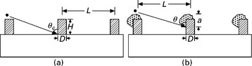
6.3 Schematic of the geometry of the seeds. (a) The cut-off angle θc is the minimum incident angle of the flux that allows global shadowing effect. (b) The exposure height a of the growing nanostructures at a fixed incident angle θ.
which is similar to the arguments by Hawkeye and Brett (2007), and Horn et al. (2004a,b). If the incident angle θ > θc, the global shadowing can affect the growth of nanostructures on each seed at the very beginning of the oblique angle deposition. In practice, the incident angle θ is much larger than θc. Therefore, we define another important geometric factor, ‘exposure height’ a, in oblique angle deposition on seeds. The exposure height determines the uniformity and morphology of the nanostructures (Ye et al., 2008). It can be defined as the portion of an individual seed or nanostructure exposed to the deposition flux incorporating the shadowing from the nearest neighbors in the plane of deposition flux and the axis of seeds, as sketched in Fig. 6.3(b). Hence, the exposure height a can be represented as
From the definition, the growing portion of the nanostructure within a should not be affected by the global shadowing from its neighbors. We suspected that the growth of the surface in this part may be controlled by the same mechanisms as that of surface growth on a seed with normal incident flux, i.e. by surface diffusion, ballistic sticking, self-shadowing, etc.
6.3 Fan-out on templated surface with normal incident flux
6.3.1 Experimental observation of fan-out growth on templated surface
We discussed the shadowing effect and developed a geometrical model to describe the shadowing effect in oblique angle deposition in the previous section in this chapter. Now we move on to the discussion of growth mechanisms with normal incident flux in experiments and Monte Carlo simulations. In this section, we reported the creation of a fan-like structure by a simple line-of-sight evaporation technique where atoms vertically drop down onto an array of nano-sized cylindrical W seeds. Very well defined fanlike clusters are formed on these seeds. The morphology of fan-like structures will be shown and analyzed from the SEM images. A ballistic deposition model will be developed to interpret the growth mechanisms of the structures.
The templated surfaces containing W pillars in a square lattice were used for the silicon (Si) depositions with normal incident flux in our experiments. The substrates were placed at a position such that their normal vectors pointed to the source. Thus, the incident angle of the flux θ is equal to 0° measured from this surface normal vector. The angular dispersion of the flux is less than 0° due to the geometry of our deposition system, i.e. the distance between the source and the substrate is about 35 cm and the diameter of the mouth of the crucible is 1 nmcm. Therefore, the flux can be assumed as a parallel flux in our experiment. Before the deposition, the area containing W pillars on the substrate was centered to the incident flux using a laser beam that simulates the incoming flux.
Si (99.9999%, Alfa Aesar) was evaporated from a graphite crucible by electron-beam bombardment as described elsewhere (Wong et al., 1987; Mei and Lu, 1988). The evaporation rate was measured by a quatz-crystal microbalance (QCM, Maxtek TM-350/400) and maintained at 5.0 ± 0.3 Å/s during the deposition by adjusting the power levels supplied to the crucible. Two sets of samples were prepared with normal thickness of 700 nm and 800 nm as measured by the QCM. To study the morphology of the samples, SEM images were taken using a field-emission SEM. The samples were coated by a ~10 nm thick Pt film to reduce the charging effect before loading into the SEM system. A very sharp tungsten tip was heated to release electrons in the SEM. The emission current ranges from 6.5 to 12.5 μA during operation. For the SEM cross-sectional views, the samples were cleaved in a direction along the axis of the square lattice. SEM top view images were also taken. The SEM images were used for further analysis using Photoshop (Adobe, Version 6.0), an image processing software.
We observed experimentally that the growth of Si on a templated substrate with a regular array of W pillars would give rise to a phenomenon referred to as ‘fan-out’ growth in normal deposition without substrate rotation (Ye and Lu, 2007a). Figures 6.4 and 6.5 demonstrate this phenomenon by the SEM top-view images and cross-sectional images of 700 nm and 800 nm thick Si films deposited on the W pillars arranged in a square lattice. Well-defined 3D fan-like structures were observed on top of each seed. If the deposition time is long enough, the nanostructures grown on the seeds will touch their neighbors, as we can see from the top-view image of those structures on the large seeds in Fig. 6.5(a). A structure with a pyramidal shape was also deposited inside the open area on the substrate between the seeds. One can see that the outlines on the side of the fans are straight and can be described geometrically by three-dimensional solid cones. Therefore, the width of the fan-like cones grew linearly with time.

6.4 SEM images of ballistic fan-like Si structures grown on a square lattice. The thickness of the Si film is 700 nm. (a) and (b) are the top-view image and the cross-sectional image of the structures on large W pillars with a 360 nm diameter, respectively. (c) and (d) are the SEM images of similar structures on small W pillars with a 150 nm diameter.

6.5 SEM images of ballistic fan-like Si structures grown on a square lattice. The thickness of the Si film is 800 nm. (a) and (b) are the top-view image and the cross-sectional image of the structures on large W pillars with a 360 nm diameter, respectively. The ballistic fans contact their neighbors and are connected as seen in (a). (c) and (d) are the SEM images of similar structures on small W pillars with a 150 nm diameter. (Adapted from Ye and Lu, 2007a, reprinted with permission.)
6.3.2 Monte Carlo simulation of ballistic fans
There has been much study of the theory on the formation (Ramanlal and Sander, 1985; Limaye and Amritkar, 1986) of this fan-like structure as well as the scaling properties (Liang and Kadanoff, 1985; Porcu and Prodi, 1991; Krug and Meakin, 1991) of the fan based on the ballistic aggregation mechanism. Although most of the studies are in two dimensions, an extension to three-dimension simulation has also been reported (Kardar et al., 1989). However, thus far very scarce experimental demonstration has been reported on the formation of this fan-like structure. In our study, a Monte Carlo (MC) simulation with nearest-neighbor ballistic sticking followed by a diffusion mechanism has been proposed to describe the fan-like structures.
Very few theoretical studies of the surface evolution concerning patterned surfaces have been carried out, mainly due to the crossover of the scales in this system. Typically, the size of individual patterns varies from tens of nanometers to several hundreds of nanometers. Each of these patterns is a result of the deposition where the atomic level surface processes and the mesoscopic processes such as mass transport cooperate to determine the growth of nanostructures on top of it. Based on this fact, the model we choose to simulate the surface growth at this scale should be able to handle the following processes (Imry, 2002):
• generating non-smooth patterned surfaces;
• multi-valued surface profiles;
• incorporation of atomic level surface processes, such as diffusion;
Ideally, multi-scale simulation techniques can provide the best solution in this situation (Castez and Salvarezza, 2006). However, in the context of limited resources, MC simulation can also address some of the issues listed above. In general, physical events including deposition of particles at random positions, surface diffusion, surface hopping, and evaporation of surface particles, can be embedded into the MC simulation.
Most recently, the importance of mass transport has been evaluated in surface growth models (Suzuki and Taga, 2001; Raible et al., 2002; van Dijken et al., 1999; Luedtke and Landman, 1989). This mass transport can be due to the inter-atomic interaction of the incoming particles and the surface particles (referred to as the ‘steering effect’), and geometric effects such as the shadowing effect. The steering effect and other growth mechanisms will be studied by 3D MC simulations. In our MC model, a 3D lattice with dimensions 1024 × 1024 × 1024 is formed by cubic lattice points. One cube represents an incident particle so that it has the dimension of a cubic lattice point. Figure 6.6 shows a schematic of the simple cubic system in this MC simulation with ballistic sticking and surface diffusion processes allowed. In the ballistic sticking model, an incident atom moving into an empty nearest-neighbor lattice point will occupy that empty position immediately. In contrast, in a solid-on-solid model, that atom will pass that empty spot unless it is the lowest position the atom can go in the system (Amar and Family, 1990). We believe that the ballistic sticking model of incident atoms comes from the inter-atomic interactions.

6.6 Schematic of 3D Monte Carlo simulation with ballistic sticking and surface diffusion processes on a smooth substrate. The flux of atoms approaches the surface from the top along the surface normal.
The interaction of atoms is due to the Lennard–Jones (L-J) potential, which is widely used, in the form of
where the parameters ε and σ depend on the properties of the atom. Using the equation developed by Raible et al. (2002), we can estimate the variation of the distance Δx from the impact point of a linear trajectory as in Fig. 6.7(b). The distance can be calculated from Raible et al. (2002) using the L-J potential for Si,

6.7 Ballistic sticking model in the MC simulations with (a) top-down and (b) oblique angle incident flux. The possible deposit sites of the incident atoms due to the ballistic sticking model and the solid-on-solid model are labeled for comparison.
For our oblique angle deposition setup, the incident angle of the particles is close to 90°, thus we can ignore the cosine part inside the square root in Eq. 6.7. If the kinetic energy E0 of the incident particle is about 0.3 eV, the integral of this equation from 0.5 to 0.55 nm yields Δx ≈ 0.455 nm. That means the particle was trapped by the surface already by the L-J potential in the form of Eq. 6.6. The approximated calculation shows that the particle will be pulled down from its trajectory when passing by an atom. This means that ballistic sticking is a good approximation in Si with very low kinetic energy.
3D MC simulations with and without ballistic sticking were performed in a cubic box with dimension N × N × N (N = 1024). The substrate containing seeds in a square lattice is fixed. The particles were injected into the system from the top and moved downward. When the particle passes by any deposited particle in its nearest-neighbor vicinity, it will stick to that particle and become its nearest neighbor (ballistic sticking model). In order to study the mechanisms of fan-out growth, we will compare the simulation results with and without ballistic sticking mechanisms. In our deposition system, the flux is very uniform due to the large distance between the opening of the crucible and the substrate. The opening of the crucible is 1 cm, and the distance is about 35 cm. So, the angle spanned by this geometry is determined to be less than 2°. In our simulations, this angular spreading of flux is taken into account as well.
In the 3D MC simulations, arrays of lattice points are selected and occupied by particles to represent the W pillars on the templated surfaces. The cylindrical seeds are placed on a smooth surface on the bottom of the simulation box with a dimension of 1024 × 1024 units and a thickness of 8 units. The seeds have a diameter of 24 units or 36 units for the small size seeds or the large size seeds, respectively. The seeds are arranged in a square lattice with a lattice constant of 256 units. The particular reason for this arrangement is to avoid overlapping on the boundary by enforcing periodic boundary conditions. This means that if a particle moves outside of the cubic system, it will re-enter from the opposite side. The height of the seeds is 80 units. Figures 6.8 (a) and (b) show the top-view and cross-sectional images of the smaller seeds, respectively. Similar images of the large size seeds are shown in Figs 6.8(c) and (d).

6.8 Templated surfaces containing seeds in a square lattice in the MC simulations: (a) top-view and (b) cross-sectional images of the small seeds 8 units in diameter. (c) and (d) are the top-view and the cross-sectional images of the big seeds with a diameter of 18 units. The height of the seeds is 80 units and the lattice constant of the square lattice is 256 units. The sizes of the images are 1024×1024 units.
First, we investigated the deposition of particles without ballistic sticking, namely, the particles approaching the surface until they are stopped by another particle deposited on the surface. When a particle is landed on the surface, a certain number K of particles, referred to as ‘diffusers’, within a cubic box with a side of 2a + 1 (a = 5) around the deposited particle are randomly selected to diffuse on the surface (Kessler et al., 1992). The number K is related to the diffusivity of material. We used the coordination numbers as the criteria of the successful diffusion. That means the diffuser will move to the new lattice point if that move increases the coordination numbers. Otherwise, it will remain at the same lattice point. The coordination numbers include the number of the nearest neighbors (NN) and the number of next-nearest neighbors (NNN) of the diffuser. Diffusion models that use NN and NNN numbers have also been adapted by other researchers (Suzuki and Taga, 2001; Stasevich et al., 2004; Johnson et al., 1994; Smilauer et al., 1993). However, our diffusion model does not include the kinetic mechanism associated with the bonding energy, which is different from the models used in molecular beam epitaxial growth (Stasevich et al., 2004; Johnson et al., 1994; Smilauer et al., 1993). The model used by Suzuki and Taga is the closest one to our model, which also deals with oblique angle deposition (Suzuki and Taga, 2001). In their approach, the site is selected from a cubic box with 3 units centered at the diffuser. The site with more coordination numbers will have a greater chance of the diffuser jumping into it according to the probability of diffusing from site A to site B:
where λ is a constant and the summation is taken over all of the allowed sites (Suzuki and Taga, 2001). After the diffuser makes a jump, it will continue the diffusion process to about 10 steps of jumping. It is not clear how the coordination numbers have been counted in the simulation model by Smy et al. (2000) for oblique angle deposition. From the precursor of their model, we know the diffusion model not only counts the coordination numbers but also the distance between the two sites. And the diffuser can jump over a long distance without staying on the surface (Dew et al., 1992). Thus, the diffuser is more likely to jump into a saddle point on the surface in the model by Smy et al. (Smy et al., 2000). Figure 6.9 shows the top-view and cross-sectional images of the structured films generated by the simulations on two types of seeds without ballistic sticking. The particles were deposited on the top area of individual seeds, as well as the substrate area between the seeds. A vertical rod-like structure is formed with uniform size. A continuous film was deposited in the gap between seeds as well. The number K in this simulation was 100, representing the diffusivity of the material. We tried other K numbers in simulations but we found that the results have no significant difference from those shown in Fig. 6.9. However, the simulated results as shown in Fig. 6.9 are different from the experimental results depicted in Fig. 6.4. That means the deposition model without ballistic sticking cannot be used to explain the fan-out growth phenomenon.

6.3.3 Growth exponent of ballistic fans
The 3D MC simulations with the ballistic sticking model have been carried out on the same pre-occupied seed arrays. The particles drop down randomly and land on the surface or stick to any particle on the surface if the two particles are within the nearest-neighbor distance. It is easy to see that after deposition the differences between the local surface heights around the newly added particle should be zero or unity in magnitude. This characteristic feature is dramatically different from the non-ballistic sticking model just discussed above and is similar to the so-called ‘restricted solid-on-solid growth’ model (Kim and Kosterlitz, 1989). With this non-trivial model, the aggregations of particles on seed arrays form ballistic fan structures as shown in Fig. 6.10. We denoted the simulation time F as the number of total particles sent into the simulation system. The snapshots of the structures were taken at a constant frequency with simulation time F = 9 × 10⁷ particles. The simulated fan structures resemble the experimental results in that the fan-out angle φ is measured to be 66° in the simulations and the experiments. They all have a dome-shaped top with rather straight outlines on the sides.
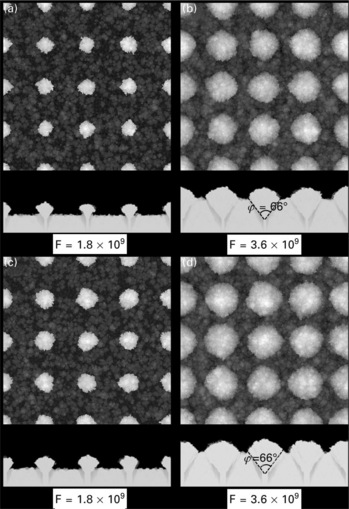
6.10 Top-view and cross-sectional snapshots of fan structures in the ballistic sticking model with normal incident flux. (a) and (b) are images of the fans on the small seeds taken at two simulation times. (c) and (d) are images of the fans on the big seeds. The diffusion parameter is set to K = 100.
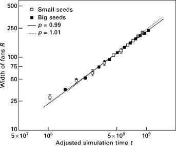
We studied the dynamic growth of the width R of the simulated ballistic fans in terms of the power law behavior, R = ktp, of the expansion of the fans in the lateral direction. The average width R of the fans was measured from the top-view images as shown in Fig. 6.10(a) and (c) plotted in Fig. 6.11. The exponent p in the power law format defines the geometrical shape of the ballistic fans. Specifically, a cylindrical shape has an exponent p = 0; a hyperbolic shape has an exponent p = 1/2 and a cone shape would have p = 1. In obtaining the p value more quantitatively from the simulations, we believe that the initial size of the cylindrical seeds has a non-trivial effect. We suppose that the size of structure is identical to the size of the seeds at the beginning of the growth. Therefore, the width R is a function of ‘adjusted time’ t instead of the real time t′, as R = ktp and t = t′ + t0. Clearly, t0 is an imaginary time that satisfies the boundary condition: R0 = kt0p, where R0 is the initial size of the seeds. After the adjustment of the time, it provides the possibility of comparing the simulated results with our experimental observations and with previous analytical and simulation results obtained using ballistic aggregation with a point seed. One can see from the plots in Fig. 6.11 that the growth of the ballistic fans has a power law behavior with the exponent p ≈ 1.0. The cone-shape geometry of the fans observed in our experiment, as shown in Fig. 6.4, is consistent with this prediction in simulations. This linear behavior is, within error, independent of the strength of diffusion, and the size of seeds. Thus, we conclude that the linear growth (p ≈ 1) of the width of the ballistic fans may be a universal characteristic of ballistic aggregation, even when diffusion is allowed.
6.4 Fan-out growth on templated surfaces with oblique angle incident flux
We discussed the ballistic sticking model to describe the fan-out growth on templated surface with normal incident flux in the previous section. Now we move on to the oblique incident case in this section. Intuitively, the morphology of structures deposited on templated surfaces should be different for the latter case due to the global shadowing effect. Nonetheless, the ballistic sticking and surface diffusion still remains as the main mechanisms that control the growth dynamics of the nanostructured films. The question we may ask is to what extent global shadowing can affect the fan-out growth on the non-flat surface. Here, we will present our answer to this important question from the experimental and modeling results.
6.4.1 Experimental demonstration of fan-out growth with oblique angle incident flux
In oblique angle deposition of Si films, the substrates with W pillars were placed at a position such that their normal vectors were turned 5° from the horizontal plane. Thus, the incident angle of the flux θ is equal to 85° with respect to this surface normal vector. The incident flux was aligned to the axis of the square lattice and the shadowing effect only comes from the nearest neighbors. The direction of the incident flux on the plane of the substrate is assigned to be the x-axis and the perpendicular direction is assigned to be the y-axis, as shown in Fig. 6.12. We observed experimentally that the fan-out growth occurs on seeds in oblique angle deposition without substrate rotation (Ye et al., 2004; Lu et al., 2005). In the ‘fan-out’ growth, the size of the nanostructures overgrows along the direction perpendicular to the incident deposition flux which is along the y-axis (or y-direction) as labeled in Fig. 6.12. The net result is that the size of the nanostructured films cannot be controlled as they grow. If the deposition time is long enough, the nanostructured films grown on the seeds will touch and merge with their neighbors from the side along the direction of the y-axis. Thus individual nanostructures cannot be distinguished along this side. Due to the shadowing effect, the gap between the seeds along the x-direction is still maintained even with the merging occurring in the y-direction.

Figure 6.13 elucidates this phenomenon by the top-view and the cross-sectional SEM images of the Si deposition on the W-pillar seeds arranged in a square lattice. Si was deposited on the templated substrate with an 85° incidence angle. The normal thickness of the growth was 2000 nm measured by the QCM. The samples were tilted to 15° when taking the cross-sectional images. The morphology of the films grown on the small size and the large size W pillars is similar to each other. The top surface of the structure is rough and has a rectangular shape with irregular sides. The structures on both of the lattices were inclined toward the source at an angle β of 53 ± 1° measured from the normal of the substrate. The size of the structures along the x-direction remained roughly constant at 340.3 ± 6.0 nm for the films grown on the square lattice seeds. From the images shown in Fig. 6.13, it is clear that the top-end surface of the structures is smoother than the surface on the sides. The side surfaces in Fig. 6.13(a) and (c) contain small fibers growing toward the source and bumpy top surfaces can be seen in Fig. 6.13(b) and (d). This suggests that the structure may be constructed by the bundling of those small Si fibers. The fan-out growth of Si films before merging is shown in Fig. 6.14(a) and (b) for the deposition on small size seeds and large size seeds, respectively. The normal thickness of the films was 800 nm as measured by the QCM. The fan-out angles φ on the seeds are measured to be 63.6 ± 0.6° and are the same for the fans on both the small and the big seeds.
6.13 Fan-out growth of Si on W pillars with 85° incident flux. (a) Top-view and (b) tilted cross-sectional SEM images of Si film grown on small W pillars; film grown on large-sized W pillars are shown in (c) and (d) for the top-view and tilted cross-sectional images, respectively.

6.14 Fan-out growth of Si on (a) small-sized W pillars and (b) large-sized W pillars. (Adapted from Ye and Lu, 2007b, reprinted with permission.)
6.4.2 MC simulations of fan-out growth with oblique angle incident flux
As we discussed above, a particle will likely be trapped by the already deposited particles through inter-atomic interactions or direct bonding. The particle will become part of the surface at first contact with the surface. In the oblique angle deposition with ballistic sticking mechanism, the global shadowing effect exists and comes into effect at every deposition event. The strength of diffusion is controlled by the pre-set number K. Figure 6.15 shows the top-view and the cross-sectional images of the structures deposited on the same templates as depicted in Fig. 6.8. The large square pictures are the top-view images while the small rectangular pictures are the cross-sectional images. In the top-view images, we can see the fan structures start to grow even in an early stage of the growth, when the number of deposited particles reaches F = 4 × 10⁷. The size of the simulation lattice is 1024 × 1024 × 1024. The incident angle of the particles is 85° in this simulation. The diffusion parameter for this set of simulations is set to K = 100, which means that there are 100 attempts at diffusion within a cycle of deposition. When the deposition time is sufficiently long, the structures connect to each other from the side perpendicular to the direction of flux. From the cross-sectional image, the top end surface declined to an angle of about 8° from horizontal. This result is similar to what we observed in experiments. A series of simulations were run with different K values.

6.15 Top-view and cross-sectional images of fan structures in MC simulation with ballistic sticking model. The incident angle of flux is 85°. The diffusion parameter is set to K = 100.
The growth of the width R of the ballistic fans was plotted as a function of the adjusted simulation time t following the method described above, as shown in Fig. 6.16. The fitting of the plots in the format of power law growth yields the growth exponent p ≈ 1 before the fans start merging with their neighbors. Combined with the observations we found in the case of normal deposition, we can conclude that the fan-like structure is a result of ballistic sticking of particles. The ballistic sticking, or ‘self-shadowing effect’, has a characteristic growth exponent p ≈ 1. We also found from the simulations that the fan-out angles decrease when diffusion increases. In the oblique angle deposition, the tilt angle of the structures increases as K increases. We measured the fan-out angle φ and the tilted angle β of the simulated structures. Compared to our experimental results, we can deduce that K = 100 fits the Si ballistic fan’s fan-out angle φ and tilted angle β, which are 65.0 ± 4.0° and 51.7 ± 0.3° respectively, in the simulated structures.

6.16 The linear growth of ballistic fans in oblique incident flux. (Source: Ye and Lu, 2007b, reprinted with permission.)
6.5 Control of fan-out growth with substrate rotations
As previous studies revealed, it is possible to create complicated nanostructured thin films by oblique angle deposition with delicate control of substrate rotation (Robbie et al., 1995a, 1996, 1998; Lakhtakia and Weiglhofer, 1995; Robbie and Brett, 1997; Kennedy et al., 2002; Zhao et al., 2002b). There are two types of nanostructures whose optical, mechanical, and electrical properties we are interested in: nanosprings and slanted nanorods. Isolated nanostructured thin films such as slanted nanorods and nanosprings could provide an ideal platform to study mechanical, electrical, thermal, and optical properties of materials on a nanometer scale. Therefore, the ability to uniformly deposit individual nanostructured thin films is of great practical value. These two structures are relatively difficult to fabricate by traditional lithographic methods, but using oblique angle deposition, we may achieve the required structures relatively more easily.
The growth of uniform slanted nanorod films on an existing array of seeds is challenging but achievable. As shown in the previous sections, the fan-out growth is intrinsic to the nature of thin film growth with strong self-shadowing effect. Therefore, fundamental research in controlling the fan-out growth has been the first priority in the development of this technique. One strategy to fabricate uniform nanostructured thin films is based on diminishing the fan-out growth by substrate rotation. During substrate rotation, some part of the growth front will be interrupted. The growth on that spot will start again at a later time or be terminated entirely, depending on the relative local height. Overall, each part of the growing surface will receive flux for a short period, effectively smoothing the growth front and resulting in uniform growth with no fan-out features even for a very long deposition time.
The geometric parameters of the structure, such as the tilt angle β with respective to the substrate normal, diameter R and separation D of the structures, can be tailored by changing the vapor incident angle θ, thus, changing their physical properties. In general, the column tilt angle β is less than the vapor incident angle θ, and follows the empirical tangent rule or cosine rule discussed above. However, the variation of the incident angle θ simultaneously changes the three geometric parameters (namely, β, R, and D), which causes some difficulty in controlling the geometry and the physical properties of the nanostructured films by simply changing the incident angle θ in oblique angle deposition. Therefore, it is desirable to have other methods to tailor the structures other than the variation of θ. Fortunately, there are some substrate rotation methods that can deposit nanostructured thin films with variable geometric parameters at a fixed incident flux angle θ in this research area.
In experiments, it is possible to control the rotation of the substrate at different rotation speeds, or change the direction or the rotation in every revolution of the substrate movement. Thus the substrate can be rotated in a non-uniform manner. By this means, the surface grows faster in some directions than others. Thus, the structure of the film will incline toward this direction. On the other hand, since the substrate is rotated, the growth front can still be interrupted and re-installed during growth which can potentially limit the fan-out growth. The shadowing direction is changed from time to time as well. We expect that the fan-out growth would be reduced by the rotation of substrate.
In this section, three substrate rotation methods are reviewed and discussed: ‘two-phase’ rotation (Ye et al., 2004), ‘swing’ rotation (Ye et al., 2005), and ‘PhiSweep’ technique (Jensen and Brett, 2005). In the ‘two-phase’ rotation method, one continuously rotates the substrate during deposition with two different speeds to finish one complete revolution. First, the substrate is rotated at a slower speed ω1 to an angle of ϕ1(< 2π) in the surface plane of the substrate, and then the speed will be switched immediately to a faster ω2 in the rest of the angle ϕ2 = 2π − ϕ1 of a complete revolution (Ye et al., 2004). The direction of rotation in these two parts is the same in the two-phase rotation technique. In swing rotation, the substrate is rotated to an angle ϕ (< 2π) in the plane of the substrate. The substrate is then rotated back to the initial position to cover one cycle of the motion (Ye et al., 2005). A similar approach of non-uniform substrate swinging was published recently by Jensen and Brett (2005). In their method, the substrate is rotated quickly to an angle and stays at that position for a period of time, then the substrate is rotated back to the original position and stays for an equal period; i.e. the substrate is rotated to the other side with the same angle and stays for the same period before it returns. This method is given the name ‘PhiSweep’ in their paper (Jensen and Brett, 2005).
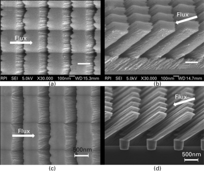
The fan-out growth on seeds is greatly reduced by the aforementioned substrate rotation techniques as shown in Fig. 6.17. For example, the Si nanorods can be grown to several micrometers without touching the neighbors from the side by the two-phase technique, as shown in Fig. 6.17(a) and (b). Uniform nanorods without fan-out growth were also demonstrated using the ‘PhiSweep’ substrate rotation method (Jensen and Brett, 2005). A set of selected SEM top-view and cross-sectional images of Si nanostructured film grown by the ‘PhiSweep’ technique are reproduced in Fig. 6.17(c) and (d) from the paper by Gish et al. (2006). Uniform nanostructured Si films on small and big seeds grown by ‘swing’ rotation are shown in Fig. 6.18. The swing angle was set at 90° and the incident angle of flux was 85° in this experiment.

6.17 Top-view and cross-sectional SEM images of uniform Si nanostructured films grown on templated surfaces by ‘two-phase’ and ‘PhiSweep’ substrate rotation techniques. (Adapted from Gish et al., 2006, reprinted with permission.)

6.18 Top-view and cross-sectional SEM images of uniform Si nanostructured films grown on small and big seeds by ‘swing’ substrate rotation.
We set up the Monte Carlo simulations to study the mechanism of reducing the fan-out growth based on the swing rotation in oblique angle deposition. Figure 6.19 shows the top-view and cross-sectional images of the Monte Carlo simulation at two different stages with swing rotation. The size of the simulation system is 1024 × 1024 × 1024. The swing angle in this simulation was fixed at ϕ = 90°. The rotation speed in this simulation was defined by the number of particles deposited in one step of substrate rotation. In our code, we change the azimuthal angles of the flux to mimic the substrate rotation because the lattice cannot be rotated. The step of increasing and decreasing this azimuthal angle is the parameter representing the substrate rotation speed. In this simulation, the rotation speed is fixed at 5000 particles per step. With swing rotation, uniform nanostructured films can be generated in our simulation of ballistic sticking of oblique incident particles on seeds (Ye and Lu, 2007b). The average tilted angle is 53.5 ± 0.3° as measured from the cross-sectional images of the structures, which is very close to the measurement in experiments. The structure grows at the beginning of the simulation and then saturates at a later simulation time to a size of 184 ± 21 lattice units when measured from the top-view images. The growth of the width R of the structures is depicted in Fig. 6.20 as a function of adjusted simulation time for the swing rotation with different swing angles. From Fig. 6.20, one can observe that the initial growth exponent is p ≈ 0.6 for all the swing angles in the simulations, as shown in the inset of Fig. 6.20. We believe that the reduction of the exponent p from 1.0 (as in the case of no substrate rotation) to less than 0.6 is due to the substrate rotation. The global shadowing affects the saturation of the width Rmax, where the well-separated structures stop fanning out with an exponent p approaching 0 (Ye and Lu, 2007b). With the global shadowing effect, increasing the swing angles will reduce the saturation width Rmax, as illustrated in the inset of Fig. 6.20.


6.20 Logarithmic plot of the width R as a function of the adjusted simulation time with different swing angles. R is saturated at a maximum value Rmax as indicated by the horizontal lines. The inset is the measurement of the exponent p and the maximum width Rmax for different swing angles. (Source: Ye and Lu, 2007b, reprinted with permission.)
6.6 Applications and future trends
The substrate rotation techniques can produce slanted nanorods of uniform sizes, which enable the fabrication of complex nanodevices, for example, arrays of nano-cantilevers. The arrays of slanted Si nanorods deposited on templated surfaces have been used to measure the mechanical properties of these nanorods. The cantilever system of atomic force microscope was used to measure the response of the Si nanorods when forces are applied to them. The results have been reported in the literature (Gaire et al., 2005). These arrays of nanorods provide an ideal system for the study of the mechanical properties of materials in nanometer size.
When a layer of slanted nanorods is deposited, the substrate can be turned 90° to deposit a second layer of slanted nanorods with the same geometry. This can be continued for many layers. Every four layers of these nanorods can form a complete turn of a square spiral as shown in Fig. 6.21. From the calculations, these spiral arrays possess a unique optical property where light with certain wavelengths cannot penetrate through the film (Toader and John, 2001). A system with this optical property is called a photonic crystal and it has rich applications in controlling of light. Recently, Si spiral photonic crystals have been deposited by the swing rotation technique (Ye et al., 2007) and the ‘PhiSweep’ technique (Summers and Brett, 2008). The properties of the photonic crystals were tested by optical measurement as well (Ye et al., 2007). However, in experiments, the Si spiral photonic crystal structures produced by oblique angle deposition cannot reach the optimized design. For optimal geometrics of Si spiral photonic crystals, the tilted angle of each arm of the structure should be as large as 65° with respect to the major axis of the spirals (Toader and John, 2002). A maximum full band gap (about 16% of the gap center frequency) can be achieved with this optimal Si structure. Therefore, in the future, the growth condition of the photonic crystals should be further explored to achieve the optimized photonic crystals. Some other materials should be tested in order to fabricate the optimized structure.
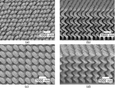
6.21 Square spirals prepared by the swing rotation on W pillars. (a) and (b) are the top-view and cross-sectional images of the spirals deposited on the triangular lattice. (c) and (d) are the top-view and cross-sectional images of the spirals deposited on the square lattice. (Source: Ye et al., 2005, reprinted with permission.)
On smooth surfaces, a layer of nanostructured thin film consisting of slanted nanorods has lower refractive index than a continuous film due to the porous nature of the film (Xi et al., 2005). The index can be varied by changing the orientation of the nanorods. It has been tested that the stacking of multiple layers of nanostructured thin films with various refractive indices has a very low reflectance and can potentially be used as an anti-reflector in several applications (Xi et al., 2007). More discussion will be presented later in this book. Although the layered films were deposited by oblique angle deposition at different incident angles, it is reasonable to extend this study using substrate rotation techniques. We would expect that the anti-reflection films are much more uniform and the refractive indices are able to be fine tuned.
In this chapter, we found that the dominant mechanism of fan-out growth is ballistic sticking that comes from the inter-atomic interactions at the atomic level. However, Monte Carlo simulation has no real dimension, so a full picture of the interactions between particles cannot be simulated. Therefore, molecular dynamics simulation might be able to handle the inter-atomic interactions. However, the system size in a typical molecular dynamics simulation is too small for the deposition of atoms on arrays of seeds. It seems that a multiscale simulation has to be developed for a better understanding of the effect of ballistic sticking in a large ensemble of atoms. In the present Monte Carlo simulation model, a simple cubic lattice is used. The extension of this simulation into other lattice structures should be interesting.
6.7 References
Ablemann, L., Lodder, C. Oblique evaporation and surface diffusion. Thin Solid Films. 1997; 305:1–21.
Amar, J.G., Family, F. Phase transition in a restricted solid-on-solid surface-growth model in 2+1 dimensions. Phys Rev Lett. 1990; 64:543–546.
Barabasi, A.L., Stanley, H.E. Fractal Concepts in Surface Growth. New York: Cambridge University Press; 1995.
Castez, M.F., Salvarezza, R.C. Modeling growth from the vapor and thermal annealing on micro- and nanopatterned substrates. Phys Rev E. 2006; 73:011607.
Dew, S.K., Smy, T., Brett, M.J. Simulation of elevated temperature aluminum metallization using SIMBAD. IEEE Trans Commun. 1992; 39:1599–1606.
Gaire, C., Ye, D.-X., Tang, F., Picu, R.C., Wang, G.-C., Lu, T.-M. A mechanical testing of isolated amorphous Si slanted nanorods. J Nanosci Nanotechnol. 2005; 5:1893–1897.
Geszti, O., Gosztola, L., Seyfried, E. Cross-sectional transmission electron microscopy study of obliquely evaporated silicon oxide thin films. Thin Solid Films. 1986; 136:L35–L38.
Gish, D.A., Summers, M.A., Brett, M.J. Morphology of periodic nanostructures for photonic crystals grown by glancing angle deposition. Photon Nanostruct. 2006; 4:23–29.
Hashimoto, T., Okamoto, K., Hara, K., Kamiya, M., Fujiwara, H. Columnar structure and texture of iron films evaporated at oblique incidence. Thin Solid Films. 1982; 91:145–154.
Hawkeye, M.M., Brett, M.J. Glancing angle deposition: fabrication, properties, and applications of micro- and nanostructured thin films. J Vac Sci Technol A. 2007; 25:1317–1335.
Horn, M.W., Pickett, M.D., Messier, R., Lakhtakia, A. Selective growth of sculptured nanowires on microlithographic lattices. J Vac Sci Technol. 2004; 22:3426–3430.
Horn, M.W., Pickett, M.D., Messier, R., Lakhtakia, A. Blending of nanoscale and microscale in uniform large-area sculptured thin-film architectures. Nanotechnology. 2004; 15:303–336.
Imry, Y. Introduction to Mesoscopic Physics, 2nd ed. New York: Oxford University Press; 2002.
Jensen, M.O., Brett, M.J. Porosity engineering in glancing angle deposition thin films. Appl Phys A. 2005; 80:763–768.
Joannopoulos, J.D., Meade, R.D., Winn, J.N. Photonic Crystals: Molding the Flow of Light. Princeton, NJ: Princeton University Press; 1995.
Johnson, M.D., Orme, C., Hunt, A.W., Graff, D., Sudijono, J., Sander, L.M., Orr, B.G. Stable and unstable growth in molecular beam epitaxy. Phys Rev Lett. 1994; 72:116–119.
Kardar, M., Parisi, G., Zhang, Y.C. Dynamic scaling of growing interfaces. Phys Rev Lett. 1989; 56:889–892.
Kennedy, S.R., Brett, M.J., Toader, O., John, S. Fabrication of tetragonal square spiral photonic crystals. Nano Lett. 2002; 2:59–62.
Kessler, D.A., Levine, H., Sander, L.M. Molecular-beam epitaxial growth and surface diffusion. Phys Rev Lett. 1992; 69:100–103.
Kim, J.M., Kosterlitz, J.M. Growth in a restricted solid-on-solid model. Phys Rev Lett. 1989; 62:2289–2292.
Krug, J., Meakin, P. Columnar growth in oblique incidence ballistic deposition: Faceting, noise reduction, and mean-field theory. Phys Rev A. 1991; 43:900–919.
Lakhtakia, A., Weiglhofer, W.S. On light propagation in helicoidal bianisotropic mediums. Proc R Soc London Ser A. 1995; 448:419–437.
Leamy, H.J., Gilmer, G.M., Dirks, A.G. The microstructure of vapor deposited thin films. Current Topics in Mat Sci. 1980; 6:309–344.
Liang, S., Kadanoff, L.P. Scaling in a ballistic aggregation model. Phys Rev A. 1985; 31:2628–2630.
Limaye, A.V., Amritkar, R.E. Theory of growth of ballistic aggregates. Phys Rev A. 1986; 34:5085–5090.
Luedtke, W.D., Landman, U. Molecular-dynamics studies of the growth modes and structure of amorphous silicon films via atom deposition. Phys Rev B. 1989; 40:11733–11746.
Lu, T.-M., Ye, D.-X., Karabacak, T., Wang, G.-C. Physical self-assembly and nano-patterning. Mat Res Soc Symp Proc. 849, 2005. [KK8.4.1-KK8.4.6].
Malac, M., Egerton, R.F., Brett, M.J., Dick, B. Fabrication of submicrometer regular arrays of pillars and helices. J Vac Sci Technol. 1997; 17:2671–2674.
Marsili, M., Maritan, A., Toigo, F., Banavar, J.R. Stochastic growth equations and reparametrization invariance. Rev Mod Phys. 1996; 68:963–983.
Meakin, P. Fractals, Scaling and Growth far from Equilibrium. New York: Cambridge University Press; 1998.
Meakin, P., Krug, J. Columnar microstructure in three-dimensional ballistic deposition. Europhys Lett. 1990; 11:7–12.
Meakin, P., Krug, J. Three-dimensional ballistic deposition at oblique incidence. Phys Rev A. 1992; 46:3390–3399.
Mei, S.-N., Lu, T.-M. A high ionization efficiency source for partially ionized beam deposition. J Vac Sci Technol A. 1988; 6:9–11.
Nakhodkin, N.G., Shaldervan, A.I. Effect of vapour incidence angles on profile and properties of condensed films. Thin Solid Films. 1972; 10:109–122.
Nieuwenheuzen, J.M., Haanstra, H.B. Microfractography of thin films. Philips Tech Rev. 1966; 27:87–91.
Porcu, F., Prodi, F. Ballistic accretion on seeds of different sizes. Phys Rev A. 1991; 44:8313–8315.
Raible, M., Linz, S.J., Hanggi, P. Growth instabilities of vapor deposited films: atomic size versus deflection effect. Eur Phys J B. 2002; 27:435–442.
Ramanlal, P., Sander, L.M. Theory of ballistic aggregation. Phys Rev Lett. 1985; 54:1828–1831.
Robbie, K., Brett, M.J. Sculptured thin films and glancing angle deposition: growth mechanics and applications. J Vac Sci Technol A. 1997; 15:1460–1465.
Robbie, K., Friedrich, L.J., Dew, S.K., Smy, T., Brett, M.J. Fabrication of thin films with highly porous microstructures. J Vac Sci Technol A. 1995; 13:1032–1035.
Robbie, K., Brett, M.J., Lakhtakia, A. First thin film realization of a helicoidal bianisotropic medium. J Vac Sci Technol A. 1995; 13:2991–2993.
Robbie, K., Brett, M.J., Lakhtakia A, A. Chiral sculptured thin films. Nature. 1996; 384:616.
Robbie, K., Sit, J.C., Brett, M.J. Advanced techniques for glancing angle deposition. J Vac Sci Technol B. 1998; 16:1115–1122.
Smilauer, P., Wilby, M.R., Vvedensky, D.D. Reentrant layer-by-layer growth: a numerical study. Phys Rev B. 1993; 47:4119–4122.
Smy, T., Vick, D., Brett, M.J., Dew, S.K., Wu, A.T., Sit, J.C., Harris, K.D. Three-dimensional simulation of film microstructure produced by glancing angle deposition. J Vac Sci Technol A. 2000; 18:2507–2512.
Stasevich, T.J., Einstein, T.L., Zia, R.K.P., Giesen, M., Ibach, H., Szalma, F. Effects of next-nearest-neighbor interactions on the orientation dependence of step stiffness: reconciling theory with experiment for Cu(001). Phys Rev B. 2004; 70:245404.
Summers, M.A., Brett, M.J. Optimization of periodic column growth in glancing angle deposition for photonic crystal fabrication. Nanotechnology. 2008; 19:415203.
Suzuki, M., Taga, Y. Numerical study of the effective surface area of obliquely deposited thin films. J Appl Phys. 2001; 90:5599–5605.
Tang, F., Liu, D.-L., Ye, D.-X., Zhao, Y.-P., Lu, T.-M., Wang, G.-C., Vijayaraghavan, A. Magnetic properties of Co nanocolumns fabricated by oblique-angle deposition. J Appl Phys. 2003; 93:4194.
Toader, O., John, S. Proposed square spiral microfabrication architecture for large three-dimensional photonic band gap crystals. Science. 2001; 292:1133–1135.
Toader, O., John, S. Square spiral photonic crystals: Robust architecture for microfabrication of materials with large three-dimensional photonic band gaps. Phys. Rev. E. 2002; 66:016610.
Tong, W.M., Williams, R.S. Kinetics of surface growth: phenomenology, scaling, and mechanisms of smoothening and roughening. Annu Rev Phys Chem. 1994; 45:401–438.
Trait, R.N., Smy, T., Brett, M.J. Modelling and characterization of columnar growth in evaporated films. Thin Solid Films. 1993; 226:196–201.
van Dijken, S., Jorritsma, L.C., Poelsema, B. Steering-enhanced roughening during metal deposition at grazing incidence. Phys Rev Lett. 1999; 82:4038–4041.
Wong, J., Mei, S.-N., Lu, T.-M. Al/Si(100) Schottky barrier formation using nozzle jet beam deposition. Appl Phys Lett. 1987; 50:679–681.
Xi, J.-Q., Kim, J.K., Schubert, E.F. Silica nanorod-array films with very low refractive indices. Nano Lett. 2005; 5:1385–1387.
Xi, J.-Q., Schubert, M.F., Kim, J.K., Schubert, E.F., Chen, M., Lin, S.-Y., Liu, W., Smart, J.A. ‘Optical thin-film materials with low refractive index for broadband elimination of Fresnel reflection. Nat. Photonics. 2007; 1:176–179.
Ye, D.-X., Lu, T.-M. Fanlike aggregations on seeds by parallel ballistic flux: experimental results and Monte Carlo simulations of the growth of three-dimensional Si structures. Phys Rev B. 2007; 75:115420.
Ye, D.-X., Lu, T.-M. Ballistic aggregation on two-dimensional arrays of seeds with oblique incident flux: growth model for amorphous Si on Si. Phys Rev B. 2007; 76:235402.
Ye, D.-X., Karabacak, T., Lim, B.K., Wang, G.-C., Lu, T.-M. Growth of uniformly aligned nanorod arrays by oblique angle deposition with two-phase substrate rotation. Nanotechnology. 2004; 15:817–821.
Ye, D.-X., Karabacak, T., Picu, R.C., Wang, G.-C., Lu, T.-M. Uniform Si nanostructures grown by oblique angle deposition with substrate swing rotation. Nanotechnology. 2005; 16:1717–1723.
Ye, D.-X., Yang, Z.-P., Chang, A.S.P., Bur, J., Lin, S.-Y., Lu, T.-M., Wang, R.Z., John, S. Experimental realization of a well-controlled 3D silicon spiral photonic crystal. J Phys D: Appl Phys. 2007; 40:2624–2628.
Ye, D.-X., Ellison, C.L., Lim, B.-K., Lu, T.-M. Shadowing growth of three-dimensional nanostructures on finite size seeds. J Appl Phys. 2008; 103:103531.
Zhao, Y.-P., Ye, D.-X., Wang, P.-I., Wang, G.-C., Lu, T.-M. Fabrication of Si nanocolumns and Si square spirals on self-assembled monolayer colloid substrates. Int J Nanosci. 2002; 1:87–97.
Zhao, Y.-P., Ye, D.-X., Wang, G.-C., Lu, T.-M. Novel nano-column and nano- flower arrays by glancing angle deposition. Nano Lett. 2002; 2:351–354.