
Epitaxial growth of graphene thin films on single crystal metal surfaces
Abstract:
Epitaxial growth of graphene on metals has been known about for five decades and has encountered renewed interest since 2006–2007 when it was realized that graphene mass production is a major hurdle in the development of graphene-based applications. With the help of model systems, i.e. prepared in clean conditions (ultra-high vacuum) and at clean surfaces (single-crystalline metallic ones), much progress has been made towards the understanding of graphene growth on metals, from the elementary processes governing growth towards the tailoring of the morphology of the graphene samples.
10.1 Introduction
Graphene is the name given to an atomically thin layer of sp2-hybridized carbon (Fig. 10.1). Its unconventional properties were explored by researchers from 2004, after it was isolated by A. Geim and colleagues. in Manchester by mechanical exfoliation of graphite (Novoselov, 2004). Such samples have fuelled exceptionally sustained research owing to their high structural quality, and they are set to keep revealing a wealth of remarkable properties resulting from the high surface to volume ratio, mechanical properties, chemical inertness, electronic band structure, etc., of graphene (Geim, 2009).

10.1 Schematics of graphene’s honeycomb structure showing the two carbon hexagonal sublattices in different shades. The unit cell is defined by the two lattice vectors represented with black arrows.
A consensus has emerged as to the necessity for alternative preparation methods, because of large deviations in the quality of samples obtained by mechanical exfoliation, and because this technique is very fastidious, together precluding the reliable and efficient production of graphene. Accordingly alternative preparation methods have been explored, among which are epitaxial growth on silicon carbide and on metals. In contrast to silicon carbide, single-crystalline metal substrates can yield high-quality graphene with one layer uniformly covering a surface (some applications then require the transfer of graphene onto an adequate support). Another direction in graphene research focuses towards understanding properties, possibly new ones, resulting from its interaction with an environment, in particular with a metal, which has obvious relevance when considering the graphene/electrode contact. Graphene prepared directly on metal surfaces, which has been known for decades (Banerjee, 1961; Karu, 1966; Irving, 1967; Presland, 1969), provides a system ideally suited to address such issues.
Growth processes are often monitored by fine inspection of a system’s structure. Therefore we first describe the structure of graphene on metals including the defects that are commonly encountered. We then focus on the growth of graphene. Throughout the discussion, we lay emphasis on the strong influence of the metal–graphene interaction upon growth processes and consequently graphene’s structure. Based on our studies of graphene growth on iridium and other contributions in the literature, we review conditions for obtaining high-quality graphene.
10.2 Structure of graphene on metals
The C–C bond is one of the strongest in nature (3.61 eV for a single bond), stronger than the bond between carbon and a noble metal. This explains why sp2 carbon (more stable than sp3) and the noble metal coexist as two separate phases, at least at room temperature and ambient (or below) pressure. As we shall discuss in Section 10.3, graphene or multilayer graphene can be obtained. The epitaxial relationship is more or less well defined: while the texture orientation is unique ([0001] direction of graphene or graphite parallel to the dense-packed metal surface normal), the azimuthal (in-plane) orientation can be multiple, either because different variants can be formed, or because the azimuthal orientation scatters around an energetically favourable situation. Graphene is the stiffest material known to date (Lee, 2008), which has important consequences for its structure: biaxial strains in graphene resulting from its epitaxial growth are restricted to a few tenths of a percent, which renders graphene’s lattice incommensurate with that of the substrate in the general case. Due to the flexibility of graphene, delaminations (wrinkles) are possible in response to thermal mismatch between the substrate and graphene. Graphene can also bend up or down at substrate edges.
10.2.1 Commensurate or not
Among transition metals, Co and Ni dense-packed surfaces exhibit only small lattice mismatches with graphene, of 1.8 and 1.2% respectively (for Fe, this is only 0.9%, but presumably due to the large solubility of C in Fe at ambient conditions, the control of the number of graphene layers on Fe is almost impossible). Considering graphene’s high Young’s modulus (Lee, 2008), stretching the graphene to match the metal lattice parameter would, however, imply that the metal can sustain a considerable amount of stress, actually more than its breaking strength. This is in apparent contradiction with experimental observations pointing to a commensurate graphene layer on the metal. This contradiction may be explained if one considers a possible change of graphene’s mechanical properties upon its bonding on the metal (which is strong on Co or Ni). Electron diffraction revealed a (1 × 1) (commensurate) superstructure for graphene/Ni(111). In this superstructure half the carbon atoms sit on top of the Ni atoms in the topmost substrate layer, and the remaining carbon atoms sit on top of the Ni atoms in the third (relative to the topmost Ni layer) substrate layer. The former carbon atoms are slightly higher than the latter (Gamo, 1997) (Fig. 10.2a).

10.2 (a) Structural model for graphene on Ni(111) derived from a fit of I-V LEED spectra (from Gamo, 1997, © Elsevier); (b) ball model for a moiré between graphene and a Ir(111) plane. Section of zigzag and armchair carbon rows are highlighted in the bottom left corner.
The situation is more complex in the case of a larger lattice mismatch between graphene and the substrate. This is the case for a number of transition metals, like Cu(111) (4% lattice mismatch with graphene), Ir(111), Pt(111), or Ru(0001) (~10%). With such substrates the coincidence of the graphene and metal surface lattices can only be local and partial: if at a given location the centres of carbon rings approximately prolong the fcc(111) or hcp(0001) atomic arrangement of the metal atoms below, a few nearest neighbour distances away, this coincidence is lost. This gives rise to a periodic lattice with the symmetry of the less symmetric surface in the {graphene,metal} system. In the case of graphene on a metallic surface with hexagonal symmetry, the superlattice exhibits hexagonal symmetry too. such lattices are encountered in various systems, such as metal/metal epitaxial systems or oxide layers on metals (see, for instance Wiederholt (1995) and Ritter (1998), respectively). Coincidence site lattices are often described following a moiré pattern (Fig. 10.2b), by analogy with the optical beating fringes appearing when looking through two thin, transparent, superimposed tissue veils (historically composed of fibres from angora goats, a type of textile whose name was adapted from Arabic to French as ‘moiré’ and to English as ‘mohair’) with similar fibre structure. For convenience and consistency with the literature, we hereafter use the term ‘moiré’.
Interesting geometric properties are associated with moirés (Amidror, 2007). It can be shown that in the case when the metal surface dense-packed directions align with < 11–20 > directions in graphene (zigzag directions), the lattice parameter of the moiré (amoiré) can be written in a simple way as a function of the lattice parameter of the metal (am) and of graphene (aC): 1/amoiré = l/aC – 1/am. This implies that amoiré is inversely proportional to the lattice mismatch between graphene and the metal. For ~ 10% lattice mismatches between graphene and the metal, amoiré is in the range of 2–3 nm, for graphene on Cu(111), amoiré was recently found to be 6.6 nm (Gao, 2010; Zhao, 2011). Note that the geometrical parameters of the moiré (orientation, lattice parameter) are very sensitive to faint variations of those of the metal and of the graphene, which allows a fine description of the graphene or metal structure (Coraux, 2008; N’Diaye, 2008b, 2009a).
Standard techniques that have been used for identifying graphene’s structure are surface science ones, most prominently low-energy electron diffraction (LEED), also scanning tunnelling microscopy (STM), and to a much lesser extent reflection high-energy electron diffraction (RHEED) or surface X-ray diffraction (SXRD). As an illustration, Fig. 10.3 shows characteristic signatures for graphene on lattice mismatched transition metals using LEED, STM and RHEED. The LEED pattern displays a sixfold symmetry, appearing as six groups of spots. The finer structure of these groups reveals two prominent spots (the outer one for the metal, the inner one for graphene) and satellites spots that arise from the moiré (N’Diaye, 2008b). STM captures the atomic structure of graphene (dark spots are centres of carbon rings) modulated by a larger scale superstructure with a periodicity in the range of 2–3 nm, which is the moiré pattern (Land, 1992). The RHEED diagrams show sets of crystal truncation rods whose streaky character point to the flatness (except for the moiré corrugation) of the surface. such patterns are observed periodically every 60°, in agreement with the sixfold symmetry of the surface. Besides the zero-order central rod, strong first-order rods are related to the graphene (inner) and metal (outer) lattices (see solid arrows in Fig. 10.3c). These main rods are surrounded by satellite ones, which are related, similar to the satellite spots in LEED, to the moiré (dotted arrows in the figure).
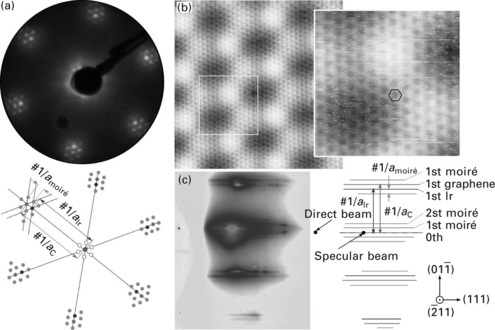
10.3 (a) LEED pattern measured with 80 eV electrons, (b) STM topographs (left: 8.8 × 8.8 nm2, right: 2.5 × 2.5 nm2), and (c) RHEED pattern recorded with 10 keV electrons, along the ![]() azimuth, for graphene on Ir(111).
azimuth, for graphene on Ir(111).
Finally, note that the above discussion applied to graphene on metal surfaces with a threefold symmetry. Much less literature addresses graphene prepared on, for example, (100) surfaces of fcc metals (Hamilton, 1980; Zhao, 2011) or (110) surfaces of body-centred cubic metals. On these metals graphene/metal moirés are also found, but their symmetry is decreased compared to that of moirés with graphene on threefold symmetric surfaces.
10.2.2 Height of the graphene sheet
The distance between the metallic surface and the graphene surface is characteristic of the metal/graphene interaction. Extreme cases for this interaction are van der Waals binding, such as in between the graphite plane, and strong hybridization of the metal d bands with the π bands of graphene. While the first case mostly preserves the conical character of graphene π bands, the second deeply modifies them, causing band gap opening at the K point in the Brillouin zone and bending of the bands. In both cases, charge transfer between graphene and the metal is a priori expected.
In the case of dominating van der Waals interactions, as in graphite, the graphene–metal distance is expected to be close to the graphite interplane distance, i.e. around 0.345 nm. In the opposite situation, the carbon and metal atoms form bonds with a covalent character, therefore the distance is expected to be much shorter (e.g. 0.21 nm for graphene/Ni(111); Gamo, 1997).
The graphene–metal distance remains poorly characterized at experimental level. This is mainly ascribed to the limitations of the techniques that are commonly employed: STM has so far been unable to disentangle topographic and electronic contributions to the apparent height measurements in the graphene–metal system (Marchini, 2007; Vazquez de Parga, 2008); atomic force microscopy (AFM) was only used in air for graphene on metals, so that the sensitivity of the technique does not allow for a sufficiently accurate determination of the height. The only techniques which proved relevant up to now are LEED I-V measurements and SXRD which were applied to graphene on Ni(111), Ru(0001), and Pt(111) (Gamo, 1997a; Martoccia, 2008; Sutter, 2009a; Moritz, 2010). The analysis of the SXRD data relies on the choice of structural models a priori, which introduces an (unknown) uncertainty in the value of the graphene–metal height. The LEED I-V analysis is based on the simulation of electron reflectivity using a dynamical diffraction framework, which allows a partial agreement between the simulations and the experiment, thus imposing careful interpretation of the simulations.
Concerning theory studies, a number of reports provide estimates of the graphene–metal distance (Bertoni, 2004; Nemec, 2006, 2008; Giovannetti, 2008; Wang, 2009; Khomyakov, 2009; Ran, 2009). Yet, noticeable deviations are found, for example for graphene/Pd(111) (Nemec, 2006; Giovannetti, 2008). It can be argued that the geometry used for the calculations is frequently over-simplified. The approximations employed to perform the ab initio calculations yield different results: the local density spin approximation is known to result in overbinding, while the generalized gradient approximation is expected to result in large graphene–metal distances as suggested by the over-estimation of the graphene–graphene distance in graphite. Most important, for a long time van der Waals interactions were not included in the calculations and are only now starting to be considered (Vanin, 2009; Lazic, 2010; Busse, 2011).
The difficulty in assessing the graphene–metal height also concerns the modulation of this height in the case of graphene–metal systems with a moiré. So far, with the exception of one experimental report (Martoccia, 2008), only demanding first principle calculations were employed in this respect (N’Diaye, 2006, 2008a, Feibelman, 2008; Wang, 2008; Brugger, 2009). From these works it seems that graphene height is modulated between 0.30 and 0.38 nm on Ir(111), a system for which graphene–metal hybridization is a priori weak (Pletikosic, 2009). On Ru(0001), the height was claimed to vary between 0.22 and 0.37 nm (Wang, 2008): for the regions where the height is lower, there is a strong covalent-like graphene–Ru interaction.
10.2.3 Orientation variants, small-angle twins and dislocations
The epitaxial relationship between graphene and the metal is well defined along the direction perpendicular to the graphene and metal surface planes: [0001] for graphite parallel to [111] (fcc metal) or [0001] (hcp metal) direction. This is not always the case in the plane of the graphene and metal surfaces, in other words, there exist several preferred azimuthal orientations for graphene on metal (orientation variants) and the orientation of graphene may fluctuate around these preferred situations. It was recently argued that the weaker the graphene–metal interaction, the less well defined should the graphene azimuthal orientation be (Sutter, 2009a).
The formation of several orientation variants was highlighted for graphene/Ir(111) for specific preparation conditions (Loginova, 2009a, 2009b), for which four orientation variants were identified (Fig. 10.4a). The azimuthal twin between each variant is large, for several to several tens of degrees. obviously, each variant represents a local minimum for the total energy of the graphene–metal system. It seems, however, that the configuration corresponding to the dense-packed metal rows aligned to the carbon zigzag edges is more energetically favourable as it always forms first and can be exclusively obtained for graphene/Ir(111) in some growth conditions. Also consistent with this larger stability is the fact that this rotation variant is more inert against oxidation (van Gastel, 2009). Rotational variants were also found for graphene/Pt(111) (Sasaki, 2000; Sutter, 2009a), but it has not been possible so far to achieve a single orientation, suggesting that all variants have comparable stability.
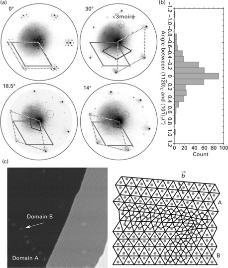
10.4 (a) Micro-LEED pattern for each of the four rotational variants for graphene on Ir(111), corresponding to a rotation of 0°, 30°, 18.5° and 14° of the carbon zigzag rows with respect to the dense-packed rows of Ir(111). The dark grey, dotted, and light grey rhombus highlight the Ir(111), graphene, and moiré unit cells, respectively (from Loginova, 2009a, © The American Physical Society, http://prb.aps.org/abstract/PRB/v80/i8/e085430). (b) Distribution of angles between the graphene zigzag rows (< 11-20 >) and the dense-packed rows (< 10-1 >) of an Ir(111) surface for the energetically preferred 0° rotational variant. (c) (left) STM topograph (108 nm × 108 nm2) showing three domains with a different orientation of graphene on Ir(111) and (right) the atomic structure of defects, such as the one indicated with an arrow on the left panel, which the grain boundaries consist of Note that the observed superstructure is the graphene/Ir(111) moiré and that it amplifies small-angle twins. A and B mark two of the domains; the arrow highlights one of the typical defects forming the grain boundary. (adapted from Coraux, 2008, © The American Chemical Society)
Depending on the growth conditions (see Section 10.3), the azimuthal orientation of graphene might be more or less well-defined around each orientation variant (N’Diaye, 2008b). The scatter in this orientations is characterized by a few tenths of a degree only for graphene/Ir(111) if graphene is prepared above 1000 °C (Fig. 10.4b), and several tens of degrees if graphene is prepared at 600 °C (Coraux, 2008). The smallest scatters can be efficiently characterized by analysing the moiré scatters, which largely amplify the carbon lattice ones (Coraux, 2008; N’Diaye, 2008a).
At the boundary between graphene domains that are twinned (scattered twins or orientation variants), the carbon lattice tends to minimize the number of dangling bonds through the formation of edge dislocations, that is pairs of a heptagon and a pentagon (Coraux, 2008) as shown in Fig. 10.4(c). Such defects are known to accommodate twin boundaries (Bollmann, 1964).
10.2.4 Other defects
Deviations from the pure two-dimensional honeycomb structure of graphene might be considered as defects. A detailed review of defects would include a discussion of their origin, stability and electronic properties, and is beyond the scope of this chapter. Defects can be intrinsic to the graphene itself, which is the case for vacancies, substitutional atoms, or graphene edges (Fig. 10.5a). They can also be extrinsic, such as being imposed by the graphene environment, which is the case for graphene undulations induced by those of the substrate (e.g., step edges) or thermally induced delaminations (Fig. 10.5b). Intrinsic defects for epitaxial graphene are so far poorly characterized. Extrinsic ones are better explored. Graphene wrinkles (linear delaminations) present after cooling samples down to room temperature following growth are due to the mismatch of thermal expansion coefficients. The wrinkle formation actually sets in at a well-defined temperature (whose value depends on the growth temperature) when cooling samples down (N’Diaye, 2009a), corresponding to a situation when strain accumulation becomes unfavourable as compared to a loss of graphene/substrate binding energy and accompanying bending energy associated with graphene delamination. such defects were first investigated for epitaxial graphene on SiC (Cambaz, 2008; Biedermann, 2009; Sun, 2009), and further for graphene on metals (Kim, 2009; Obraztsov, 2007; Chae, 2009; Loginova, 2009a; N’Diaye, 2009a; Sutter, 2009a). Their nucleation occurs abruptly within a fraction of a second, presumably at the location of defects in graphene or around substrate step edges where the graphene lattice is already bent (Chae, 2009). Their propagation is to the contrary progressive (Sutter, 2009a). The formation of wrinkles (when cooling down the sample from growth temperature) and their suppression (upon heating up the sample again) were shown to take place at distinct temperatures, pointing to a hysteresis.

10.5 (a) Vacancies (missing atom in the carbon lattice), substitutional atoms (replacing a carbon one, shown with a larger radius), and graphene edges (black: zigzag, grey: armchair); (b) wrinkle formed in graphene following delamination from the substrate (not shown).
The bending of the graphene lattice by the substrate step edges (the graphene lattice is not interrupted by the step edges) was mainly addressed for graphene in epitaxy on metals, for both Ru(0001) (Pan, 2007) and Ir(111) (Coraux, 2008) substrates. The graphene lattice was shown to be continuous across the substrate step edges. On Ir(111) the radius of curvature could even be evaluated by taking benefit of the graphene/Ir(111) moiré and its high sensitivity to sub-Ångström displacements. It was found to be close to that of thinnest single wall carbon nanotubes, i.e. approximately 0.27 nm.
10.3 Growth of graphene on a metal
In discussing graphene growth on metals, one may consider several situations, first depending on the nature of the carbon source and the way it is provided, then depending on the affinity of carbon with the metal substrate. Both aspects can be linked. For instance, carbon solubility in Ni is of the order of 1 at% at 1000 °C, a temperature which is often used for graphene growth on Ni, and drastically drops at lower temperature, so that graphene growth can proceed from segregation of carbon dissolved in bulk Ni, which may be eased by slow cooling of Ni from ~ 1000 °C down to room temperature (after Ni has been enriched with carbon at high temperatures if required) (Kim, 2009). On the contrary, Ir can store much less carbon in its bulk (Arnoult, 1972), which implies that graphene growth proceeds only by impinging carbon adspecies supplied to the surface.
A variety of carbon sources can be employed for the growth, and it is probable that others will be used in the future. The most convenient source is a gas of carbon-containing molecules (Fig. 10.6a). Such molecules are usually hydrocarbons (Oshima, 1997). Until 2009, the gases were injected at low-pressure in ultra-high vacuum systems (UHV). In 2009, gas mixtures (e.g. CH4/Ar/H2) were also employed at ambient pressure (Kim; 2009; Reina, 2009a), opening valuable perspectives for graphene production. In both cases (UHV and ambient pressure) the carbon-containing molecules are cracked at the metal surface; for this the metal surface is made catalytically active by heating it. This process can be considered an heterogeneous chemical reaction between a gas phase and a solid one, which is why the technique is often referred to as chemical vapour deposition (CVD). Another option for graphene growth is the use of an atomic carbon source (Loginova, 2008). Finally, in the case of metals having a non-negligible carbon solubility, carbon segregation from the bulk towards the surface might be an alternative route (Sutter, 2008).

10.6 Schematics for the different elementary processed during CVD growth of graphene on a metal, with a methane precursor as an illustration. (a) A methane molecule is adsorbed at the surface, cracked into a carbon adatom, leaving two hydrogen molecules released in vacuum. (b) The carbon adatom diffuses at the surface (or sub-surface). (c) The carbon adatom incorporates in a carbon chain, forming a pentamer (on metal surfaces like Ir(111) or Ru(0001), Loginova, 2008). (d) The carbon chain diffuses at the surfaces and (e) is incorporated in the graphene flake.
In the following we focus on the growth processes disregarding the way the carbon ad-species have been formed at the metal surface (CVD, atomic carbon source, segregation). This is legitimate if the nature of the carbon source only affects graphene growth through the rate of adatom formation. This is at least the case in prototypical systems that are suited to address elementary growth processes, for instance growth by CVD with ethene or by an atomic carbon source at single-crystalline metal surfaces (Loginova, 2009b).
10.3.1 Growing graphene nanoflakes
A derivative of the CVD growth for graphene consists in (i) adsorbing carbon-containing molecules at the metallic surface, at such a temperature that the molecules do not desorb to vacuum, and (ii) increasing the sample temperature for promoting hydrocarbon decomposition and eventually graphene growth (Coraux, 2009).
The surface is first saturated with molecules, and the resulting adlayer prevents the strong bonding of further molecules at the surface. In practice, ethene molecules are transformed into ethyledine ones at Pt(111) and Ir(111) (Nieuwenhuys, 1976) surfaces at room temperature. The amount of carbon in the resulting adlayer is less than that in a full graphene layer, due to steric effects.
In the next step the substrate is heated up. In the course of increasing the sample temperature, dehydrogenation of the molecules proceeds, leaving pure-carbon adspecies being mobile at the surface. Nanometer-scale carbidic islands develop from this carbon sea. The electronic interaction between the carbidic islands and the metal surface is strong, all the more as the islands are small, as has been shown for graphene on Ir(111). This is because in small islands the proportion of edge atoms is large: such low coordinated atoms have a tendency to form bonds with the metal atoms underneath. This strong bonding was detected through energy shifts in the carbon and metal atoms core levels. As a result of the enhanced bonding of graphene edges to the substrate, the small graphene islands were shown to be dome-shaped and characterized by a small distance to the metal surface, noticeably below that for a plain graphene sheet on Ir(111), for island radii smaller than 1–2 nm, and all the more as the radii is small (Fig. 10.7) (Lacovig, 2009). Such small islands, as imaged by STM (Fig. 10.8a), are found at the terraces of the metallic surface, and occasionally bond to substrate step edges. They are characterized by a poorly defined height and rounded edges. Further increase of the temperature modifies their morphology (Fig. 10.8b–e). Their height becomes well defined as seen by STM for islands radii larger than a few nanometres.

10.7 Calculated structural models for graphene nanoislands on Ir(111) as a function of their (small) size, on a side view and on a top view: for (a) one, (b) three, (c) seven, and (d) 19 carbon rings. Note that the average height of the islands increases with their size. (from Lacovig, 2009, © The American Physical Society, http://prl.aps.org/abstract/PRL/v103/i16/e166101)

10.8 (a–e) STM topographs of typical carbidic (below 600 °C) and graphene (higher temperatures) islands on Ir(111) as a function of the growth temperature: (a) 600 °C (3.2 × 3.2 nm2), (b) 700 °C (6.2 × 6.2 nm2), (c) 850 °C (18 × 18 nm2), (d) 1050 °C (32 × 32 nm2), and (e) 1200 °C (64 × 64 nm2). The size of the white box in (b–e) corresponds to the size of (a) (from Coraux, 2009, © Institute of Physics). (f) STM topograph (73 × 73 nm2) of a graphene island grown on Ir(111) and presumably formed upon the coalescence of smaller islands.
Such islands with well-defined height are bound by straight edges that are precisely oriented along the < 11-20 > directions of graphene, consistent with the prominent proportion of zigzag portions composing these edges. At sufficiently high growth temperature, it was shown for graphene on Ir(111) that the island edges align to the < 1-10 > direction of Ir(111) (N’Diaye, 2008b). Graphene islands were also reported on Pt(111) (Land, 1992), Ir(111) (N’Diaye, 2006; Coraux, 2009), and Co(0001) (Eom, 2009). The occurrence of straight edges for graphene is the evidence that carbon mobility is active at edges. In the explored growth temperature range (700–1300 °C), these effects are rather slow as the islands are most often not in their equilibrium, hexagonal shape. Carbon diffusion at edges could proceed through that of carbon pentagons continuously formed at graphene edges during growth (Frenklach, 2004; Whitesides, 2010). Pentagon collisions result in hexagons, i.e. graphene building blocks (Whitesides, 2007). On the contrary, edge smoothing through a 2D carbon gas surrounding the edges, that would be formed via carbon atom detachment at edges (more readily at regions where the 2D pressure is higher, i.e. at convex edges), is not a prominent process at the temperature of interest.
The temperature to which the substrate is heated up determines the size of the graphene islands: their average diameter can be adjusted between a few and several tens of nanometres for 600 °C and 1200 °C respectively on Ir(111). Through this temperature range, the island density drops by almost three orders of magnitude, consistent with the fact that the total amount of carbon at the surface is not modified. As the growth temperature increases, the proportion of graphene islands bound to substrate step edges increases. The density and size of the graphene islands vary because of a thermally induced ripening process. Considering the strength of the C–C bond in graphene, Ostwald ripening, i.e. the preferential growth of large islands at the expense of the dissolution of smaller ones through their higher pressure of carbon adatoms, cannot account for the observed efficient ripening below 1300 °C. The presence of large islands with irregularly shaped (though zigzag) edges, exhibiting large vacancies, for growth temperature of 850 °C during a few seconds (Fig. 10.8f), suggests that large islands are formed upon the coalescence of smaller ones that are mobile at the surface (Coraux, 2009). This process is known as smoluchowski ripening. It is probably effective due to the incommensuracy of the graphene and metal lattices. For a strictly incommensurate island the activation energy for lateral motion would vanish, as for every carbon moving away from its optimum binding site, another one finds it. The existence of a migration barrier is probably linked to the stronger binding of the graphene island edge atoms to the substrate. As larger graphene islands display sizes consisting of an integer number of moiré units it is likely that the graphene edges bind to specific energetically preferred substrate sites. Prolonged heating results in islands becoming more compact, presumably due to efficient carbon mobility at graphene edges.
10.3.2 Growing plain graphene sheets
We now consider the situation where carbon atoms, whatever their source, are provided at the hot metallic surface.
From graphene islands to plain sheets
Graphene islands preferentially bind to the substrate step edges. The size (density) of the islands is the larger (lower) the higher the growth temperature. This is evidence that graphene nucleation along the steps is homogeneous and not at a specific defect site. The nucleation at step edges was observed by STM (Fig. 10.9a) and low-energy electron microscopy (LEEM) on Ir(111) (Coraux, 2009), Ru(0001) (Sutter, 2008), and Pt(111) (Sutter, 2009a), in a wide range of growth temperatures, and for different types of carbon sources. The graphene islands nucleate preferentially at the ascending side of the step edge.As discussed in the next subsection, this is presumably promoted by the fact that carbon atoms attach via σ bonds to the ascending substrate step.
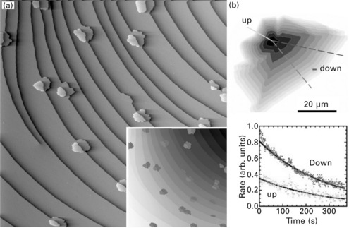
10.9 (a) Differentiated STM topograph (1 × 1 μm2) of graphene islands nucleated at Ir(111) atomic step edges (the islands are highlighted in dark and light gray if nucleated at the upper or lower terrace respectively) (from Coraux, 2009, © Institute of Physics). (b) Contours of a growing graphene island on Pt(111) at the vicinity of an atomic substrate step edge, as a function of the growth time, as images with LEEM (top panel) and growth rate derived from such a sequence of images at the upper and lower terrace around the step edge. (from Sutter, 2009a, © The American Physical Society, http://prb.aps.org/abstract/PRB/v80/i24/e245411)
Providing more carbon adatoms at the surface results in the growth of the islands. This growth is always anisotropic, faster at the lower terrace than at the upper one. For graphene on Ru(0001), there is almost no growth at the upper terrace (Sutter, 2008). On Ir(111) and Pt(111) (Coraux, 2009; Loginova, 2009b; Sutter, 2009a) the onset of growth is delayed (Fig. 10.9b). Probably it is delayed by an energetically costly transient state, for which the carbon–metal bond is broken before a carbon–carbon bond is formed across the substrate step edge. The growth of graphene over steps does not interrupt the graphene lattice. The carbon rows are continuous and bent vertically to adapt to the the terrace flow (Pan, 2007; Coraux, 2008); in other words, graphene rests like a blanket on the substrate.
Growing islands will eventually meet. STM showed that the moiré displays continuous rows through the location where the islands coalesced, which is evidence that the carbon rows are also continuous (Coraux, 2009). This observation is puzzling at first glance, as there is no reason why the graphene lattices from the two lattices would be in registry. Rather we would expect a shift by a fraction of a lattice constant. Lattice distortions, which could be adapted either locally or at a larger scale, are therefore expected. Dislocations (heptagon-pentagon pairs) are also found where the islands met to accommodate for small tilts between the islands.
Prolonged growth will result in a lateral expansion of the graphene flakes which will meet and eventually cover the whole metallic surface. This is discussed in more detail on page 245.
Graphene interaction with the substrate step edges
The nucleation of graphene at substrate step edges and the partial or total hindering of uphill growth over step edges are evidence for the interaction of graphene edges with substrate steps. This interaction is probably lowering the edge energies of both graphene and the metal by increasing the low coordination of edge atoms.
Graphene growth was also observed to induce reshaping of the substrate step edges. The magnitude of this reshaping varies. On Ir(111) or Ru(0001) (Coraux, 2009; Loginova, 2010), it is in the form of a reorientation of the metal step edge that is in contact with one of the graphene island edges, so that the metal edge transforms into segments aligning the zigzag direction of graphene (Fig. 10.10a). On Pt(111) and Pd(111), the effects are much stronger: a whole graphene island can penetrate the metal terraces so that all graphene edges are bound to metal edges, with the latter aligning graphene’s zigzag edges (Nakagoe, 2002; Fujita, 2005; Land, 1992; Kwon, 2009) (Fig. 10.10b). Such processes can only be effective if flow of metal atoms develops at the step edges. The preferential orientation of the reshaped metal edges is probably driven by maximization of the number of carbon–metal σ-bonds.

10.10 STM topographs evidencing the interaction of metal step edges upon graphene growth, on Ir(111) (a) and on Pd(111) (b) (from Kwon, 2009, © The American Chemical Society). The superstructure is the moiré of graphene/Ir(111) and graphene/Pd(111). The inset in (a) highlights the structure of the substrate step edge reshaped by the graphene island. The interaction of graphene with Pd(111) steps is such that the graphene island is incorporated into a Pd terrace. Image sizes are 125 × 125 nm2 for (a) and 380 × 250 nm2 for (b).
So far only in the cases of Ni(111) (Helveg, 2004) and Ru(0001) (Loginova, 2010) supports has it been shown that a growth front of graphene is possible also at the location where it is attached to a metallic step edge. Accordingly graphene grows at the expense of a retraction of the substrate step edge (Fig. 10.11). It was argued (Loginova, 2010) that the metal atoms are then displaced away from the step edge and can incorporate in the topmost metal layer, causing the formation of a dislocation network pattern in this layer. Metal step edge retraction may also result from the equilibrium between the step edge and the 2D metal gas surrounding it at the growth temperature, allowing for an efficient exchange between step atoms and adatoms.

10.11 In situ observation of carbon nanotube growth at the surface of a catalytic (Ni) particle with transmission electron microscopy, where methane is provided with increasing doses from (a) to (c). Scale bar is 5 nm. The schematics highlight the graphene growth at the expense of the retraction of the substrate step edges. (from Helveg, 2004, © Nature Publishing Group)
Elementary processes during the growth
As we already discussed, graphene growth starts at the step edges. It was shown that the amount of graphene does not depend on the size of the terraces surrounding the step edges (Coraux, 2009). In addition, at steps graphene islands nucleate with random separations giving rise to earlier coalescence. These observations indicate the absence of any significant gradients induced in the concentration of the adspecies from which the islands grow. Graphene island growth is not diffusion limited.
On the contrary, it was proposed that the growth is interface limited because carbon adatoms experience a large energy barrier for attaching to graphene step edges (Loginova, 2008). A large carbon supersaturation is needed at the surface so that several atom carbon clusters, being mobile at the surface, can be formed. Such clusters have been calculated to possess a much lower energy barrier for attachment at graphene edges, and are thus considered as building blocks for graphene growth. They are as large as heptamers on Ru(0001) (Loginova, 2008) and Ir(111) (Loginova, 2009b). These results are qualitatively very similar for two different carbon sources, CVD with ethylene or atomic carbon flux.
The analysis of the surface coverage with graphene as a function of the carbon dose provides information about the stability of carbon adspecies at the bare metal surfaces and regions covered with graphene. For growth on Ir(111), it was shown that the experimental data are well reproduced by a mere exponential law (Fig. 10.12), with a rapid increase at initial stages followed by a slowing down of the growth rate towards zero as full coverage is approached (Coraux, 2009). Quantitative analysis showed that the exponential behaviour is well reproduced by assuming (i) the absence of desorption of carbon adspecies from the Ir surface areas, (ii) the absence of C incorporation to the bulk and (iii) no sticking of molecules or C adspecies to the graphene areas. Therefore, under these conditions graphene growth is self-limiting and terminates upon monolayer completion. In the opposite situation where the bulk of the support has the capability to store carbon and supply mobile species, like it is the case from 1500 °C on Ir(111) or 800–900 °C on metals like Ni or Ru, the graphene growth is not self-limiting. A second and even more layers may form underneath the monolayer graphene.
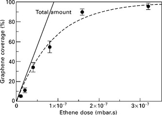
10.12 Graphene coverage as a function of the ethene dose during CVD growth of graphene on Ir(111), as estimated from STM topographs, and exponential law fit. (adapted from Coraux, 2009, © Institute of Physics).
On the formation and stability of rotational variants
Graphene rotational variants are found at Ir(111) and Pt(111) surfaces (see Section 10.2.3), and will presumably also be found at the surface of other metals weakly interacting with graphene, typically those for which the average graphene–metal distance is close to that between planes in graphite. On Ir(111) the variant with graphene zigzag edges aligned to Ir dense-packed rows grows is energetically preferred and dominates the growth; at high growth temperatures and fluxes, other variants may nucleate at its edges (Loginova, 2009b). For graphene on Pt(111) the different variants nucleate independently and at the same time (Sutter, 2009a). On Ir(111), it was suggested that the nucleation of the other variants is heterogeneous, taking place at defects at the first variant edges. Once the other variants are nucleated, they grow faster than the first variant. It was argued that this is due to different carbon attachment kinetics at graphene edges for the different variants, as carbon attachment is the limiting step in graphene growth (Lovinova, 2009b).
The growth of other variants can be suppressed if the development of graphene edges not aligned to the dense-packed rows of the substrate can be avoided, or at least largely postponed. For this, a fraction of the surface might first be covered by graphene islands having well-defined zigzag edges following the recipe described in Section 10.3.2 (pre-adsorption of ethene at room temperature followed by high temperature annealing). Accordingly a high density of islands is achieved, and the growth can be continued by CVD at high temperature, yielding exclusively the more stable and energetically preferred variant (van Gastel, 2009). In practice, the first step may be performed at 1200 °C and the second at 800 °C, which results in a single crystallographic orientation of graphene across the whole sample surface. The as-grown graphene has a low density of wrinkles (see Section 10.2.4) due to the low growth temperature of 800 °C during graphene layer completion. The lower growth temperature induces less thermal lattice mismatch during cooling and consequently less strain relieving defects.
The different variants have distinct stabilities, as suggested by the preferential high temperature oxygen etching of the graphene variants of which the zigzag edges do not align to dense-packed rows in the metal (van Gastel, 2009; Starodub, 2010). This difference in reactivity was employed as an alternative route to achieve macroscopic graphene samples with a single orientation on Ir(111), via cycles of CVD growth with ethylene and oxygen etching of the undesired variants (van Gastel, 2009) (Fig. 10.13).

10.13 Repeated sequences (a–d) of CVD growth of graphene on Ir(111) and selective high temperature (856 °C) oxygen etching (at a partial pressure of 5 × 10‒8 mbar), as observed in situ by photoemission electron microscopy (field of view, 102 μm). The rotational variant with carbon zigzag rows parallel to dense-packed rows of Ir(111) appear brighter, while the other variant appears in grey. Ir(111), due to its high work function, appears in black. The procedure leads to the selective etching of the second variant and to the prominent formation of the first one with a 99% yield (from van Gastel, 2009, © American Institute of Physics)
10.3.3 Graphene multilayers on metals
Graphene multilayers are commonly obtained on metals which can store a non-negligible amount of carbon in their bulk. This is the case for instance for Ru, Ni or Co. Relatively slow cooling rates (typically 10 °C/s, but this figure depends on the amount of C stored in the metal) are usually employed to promote the diffusion of carbon towards the bulk of the metal, leaving only a limited amount of carbon close to the metal surface, which favours the growth of few-layer and even single layer graphene (Yu, 2008; Reina, 2009b). Too slow cooling rates leave too much time for carbon to diffuse towards the metal bulk, resulting in negligible amounts of carbon near the surface and accordingly no graphene growth by segregation. on the contrary, fast cooling rates inhibit carbon diffusion towards the bulk, so that large amounts of carbon are available close to the surface of the metal: this favours the growth of multilayer and defective graphene. LEEM showed that an additional graphene layer starts to grow after each layer is completed (Sutter, 2009b, 2009c). So far the question of how the second layer of graphene grows after the first is completed remains open: on Pt(111) it was shown that the second layer does not grow between the first layer and the topmost Pt layer (Sutter, 2009a), pushing the first layer upwards, which suggests that carbon atoms are escaping the bulk towards the graphene surface via defects (e.g. holes) present in the first graphene layer. LEEM studies showed that the graphene growth by segregation is mostly a bulk-diffusion limited process (McCarty, 2009). Multilayers and the number of layers they contain are readily identified by electron reflectivity as was done for multilayer graphene on SiC (Ohta, 2008). The in-plane morphology of multilayer graphene is much less studied. The stacking of the multilayers and azimuthal orientation between layers are, for instance, not reported or discussed. Diffraction experiments, such as (micro) low-energy electron diffraction (Sutter, 2008), should provide valuable hints in this respect. STM was used to show that the second layer in a bilayer might exhibit nanometre scale ripples at the surface or be flat depending on the location on the sample (Sutter, 2008, 2009c).
At the surface of metals with low carbon solubility such as Ir or Pt, the formation of multilayer graphene is generally absent, since once the surface is covered with graphene, the graphene growth reaction stops. at high temperatures also in these metals carbon can be stored in the bulk, yet in much lower proportions than in Ni or Ru. Cooling down leads to the segregation of this carbon exclusively at the location of defects in the first graphene layers (e.g. holes, substrate step bunches), promoting the local growth of multilayer graphene (Sutter, 2009a). It seems that only small multilayer domains (with extensions of a few microns), rather than large surfaces, can be obtained that way (Sutter, 2009a; Starodub, 2010; Meyer zu Heringdorf, private communication).
10.4 Future trends
An important direction for research is the growth of graphene on thin metallic films. This is the first step towards cheap graphene production on a large scale (Bae, 2009) which may be followed by the transfer of the graphene onto suitable supports following the etching of the metallic film (Kim, 2009; Reina, 2009a). So far polycrystalline thin films were employed in this context, yet the electronic properties of the samples are remarkably high. Controlling the number of graphene layers, ultimately down to a single one, and the crystallinity of the lattice to further increase the electronic performance will require the optimization of the growth conditions (Li, 2010) and the use of metallic thin films with much better structural quality. Educated choices for the nature of the metallic films should also allow better control of the number of layers (Li, 2009) and reducing the growth temperatures which are prohibitively high at present (~1000 °C). In this latter respect the plasma-enhanced growth, which provides carbon species in an already active form at the surface, is a promising approach, which is not only applied on metal surfaces (Ismach, 2010; Rümmeli, 2010). Graphene growth on metals from metallic carbon sources is also an interesting alternative route (Hofrichter, 2009; Juang, 2009; Xi, 2011).
The experimental investigation of the interaction between graphene and the metallic surface has made significant progress in the last few years, noticeably concerning the charge transfer between the two materials and the carbon–metal hybridization, thanks to transport measurements (Huard, 2008; Blake, 2009), photoemission spectroscopy (Oshima, 1997; Gruneis, 2008; Varykhalov, 2008; Pletikosic, 2009; Lacovig, 2009; Sutter, 2009b), and ab initio calculations (Nemec, 2006, 2008; Giovannetti, 2008; Wang, 2009; Khomyakov, 2009; Ran, 2009). Yet many questions remain open. The effort to include van der Waals interactions in ab initio simulations has just been initiated (Vanin, 2009) and is mandatory for quantitative understanding of graphene–metal interaction in the case of weakly bound systems. The identification of general trends explaining the different interactions, from chemisorption to physisorption is in progress at the moment (Khomyakov, 2009). The connection between the strength of the graphene–metal/carbon–metal interaction and the growth and structure of graphene is not clearly understood so far, and should become more obvious once growth and structure of graphene have been studied at elementary scales on a wider variety of substrates.
The moiré lattices between graphene and transition metal surfaces were shown to be quite efficient patterns for the self-organization of a variety of nanometer size clusters. It was initially proven on Ir(111) substrates (N’Diaye, 2006, 2009b) and later on Ru(0001) (Donner, 2009; Pan, 2009; Zhang, 2009). Novel magnetic, catalytic, or optical effects are being considered in these systems.
10.5 Sources of further information and advice
Few reviews address graphene growth on metals (Wintterlin, 2009; Oshima, 1997), on SiC (de Heer, 2007), and by chemical ways (Park, 2009). The unconventional electronic properties of graphene were reviewed in a comprehensive article (Castro Neto, 2009). More accessible reviews on this aspect also exist (Geim, 2007; Katsnelson, 2007). A point of view on the prospects of graphene research and applications was proposed by Geim (2009).
Worth mentioning in the context of this chapter, which is devoted to graphene on metals, are spintronics effects in this system. Efficient spin-polarization and filtering were predicted (Karpan, 2007, 2008; Yazyev, 2009) and have started to be explored at the experimental level (Dedkov, 2008a). Rashba effects developing at the graphene–metal interface were recently the matter of noticeable interest (Dedkov, 2008b; Varykhalov, 2008; Rader, 2009; Rashba, 2009; Kuemmeth, 2009).
10.6 Acknowledgements
Johann Coraux acknowledges the Alexander von Humboldt Foundation for a research grant.
10.7 References
Amidror, I., The Theory of the Moiré Phenomenon. Springer, Dordrecht, 2007.
Arnoult, W.J., McLellan, R.B. The solubility of carbon in rhodium, ruthenium, iridium and rhenium. Scr. Metall.. 1972; 6:1013.
Bae, S., et al. 30-inch roll-based production of high quality graphene films for flexible transparent electrodes. Sci. Technol.. 2009; 5:1.
Banerjee, B.C., Hirt, T.J., Walker, P.L., Jr. Pyrolitic carbon formation from carbon suboxide. Nature. 1961; 192:450.
Bertoni, G., Calmels, L., Altibelli, A., Serin, V. First-principles calculation of the electronic structure and EELS spectra of the graphene/Ni(111) interface. Phys. Rev. B. 2004; 71:075402.
Biedermann, L.B., Bolen, M.L., Capano, M.A., Zemlyanov, D., Reifenberger, R.G. Insights into few-layer epitaxial graphene growth on 4H-SiC(0001) substrates from STM studies. Phys. Rev. B. 2009; 79:125411.
Blake, P., et al. Influence of metal contacts and charge inhomogeneity on transport properties of graphene near neutrality point. Solid State Comm.. 2009; 149:1068.
Bollmann, W. Some basic problems regarding subgrain boundaries. Discuss. Faraday Soc.. 1964; 38:26.
Brugger, T., et al. Comparison of electronic structure and template function of single-layer graphene and a hexagonal boron nitride nanomesh on Ru(0001). Phys. Rev. B. 2009; 79:045407.
Busse, C., et al. Graphene on Ir(111): a weakly bonded system, 2011. [Submitted].
Cambaz, Z.G., Yushin, G., Osswald, S., Mochalin, V., Gogotsi, Y. Non catalytic synthesis of carbon nanotubes, graphene and graphite on SiC. Carbon. 2008; 46:841.
Castro Neto, A.H., Guinea, F., Peres, N.M.R., Novoselov, K.S., Geim, A.K. The electronic properties of graphene. Rev. Mod. Phys.. 2009; 81:109.
Chae, S.J., et al. Synthesis of large-area graphene layers on poly-nickel substrates by chemical vapor deposition: wrinkle formation. Adv. Mater.. 2009; 21:2328.
Coraux, J., N’Diaye, A.T., Busse, C., Michely, T. Structural coherency of graphene on Ir(111). Nano Lett.. 2008; 8:565.
Coraux, J., et al. Growth of graphene on Ir(111),. New J. Phys.. 2009; 11:023006.
Dedkov, Y.S., Fonin, M., Laubschat, C. A possible source of spin-polarized electrons: the inert graphene/Ni(111) system. Appl. Phys. Lett.. 2008; 92:052506.
Dedkov, Y.S., Fonin, M., Rüdiger, U., Laubschat, C. Rashba effect in the graphene/Ni(111) system. Phys. Rev. Lett.. 2008; 100:107602.
de Heer, W.A., et al. Epitaxial graphene. Solid State Comm.. 2007; 143:92.
Donner, K., Jakob, P. Structural properties and site specific interactions of Pt with graphene/Ru(0001) moiré overlayer. J. Chem. Phys.. 2009; 131:164701.
Eom, D., et al. Structure and electronic properties of graphene nanoislands on Co(0001). Nano Lett.. 2009; 9:2844.
Feibelman, P.J. Pinning of graphene to Ir(111) by flat Ir dots. Phys. Rev. B. 2008; 77:165419.
Frenklach, M., Ping, J. On the role of surface migration in the growth and structure of graphene layers. Carbon. 2004; 42:1209.
Fujita, T., Kobayashi, W., Oshima, C. Novel structures of carbon layers on a Pt(111) surface. Surface and Interface Analysis. 2005; 37:120.
Gao, L., Guest, J.R., Guisinger, N.P. Epitaxial graphene on Cu(111). Nano Lett.. 2010; 10:3512.
Gamo, Y., et al. Atomic structure of monolayer graphite formed on Ni(111). Surf. Sci.. 1997; 374:61.
Geim, A.K. Graphene: status and prospects. Science. 2009; 324:1530.
Geim, A.K., Novoselov, K.S. The rise of graphene. Nature Mater.. 2007; 6:183.
Giovannetti, G., et al. Doping graphene with metal contacts. Phys. Rev. Lett.. 2008; 101:026803.
Grüneis, A., Vyalikh, D.V. Tunable hybridization between electronic states of graphene and a metal surface. Phys. Rev. B. 2008; 77:193401.
Hamilton, J.C., Blakely, J.M. Carbon segregation to single-crystal surfaces of Pt, Pd and Co. Surf. Sci.. 1980; 91:199.
Helveg, S., et al. Atomic-scale imaging of carbon nanofibre growth. Nature. 2004; 427:426.
Hofrichter, J., et al. Synthesis of graphene on silicon dioxide by a solid carbon source. Nano Lett.. 2009; 10:36.
Huard, B., Stander, N., Sulpizio, J.A., Goldhaber-Gordon, D. Evidence of the role of contacts on the observed electron–hole asymmetry in graphene. Phys. Rev. B. 2008; 78:121402(R).
Irving, S.M., Walker, P.L., Jr. Interaction of evaporated carbon with heated metal substrates. Carbon. 1967; 5:399.
Ismach, A., et al. Direct chemical vapor deposition of graphene on dielectric surfaces. Nano Lett.. 2010; 10:1542.
Juang, Z.-Y., et al. Synthesis of graphene on silicon carbide substrates at low temperature. Carbon. 2009; 47:2026.
Karpan, V.M., et al. Graphite and graphene as perfect spin filters. Phys. Rev. Lett.. 2007; 99:176602.
Karpan, V.M., et al. Theoretical prediction of perfect spin filtering at interfaces between close-packed surfaces of Ni or Co and graphite or graphene. Phys. Rev. B. 2008; 78:195419.
Karu, A.E., Beer, M. Pyrolytic formation of highly crystalline graphite films. J. Appl. Phys. 1966; 37:2179.
Katsnelson, M.I. Graphene: carbon in two dimensions. Materials Today. 2007; 10:20.
Khomyakov, P.A., Giovannetti, G., Rusu, P.C., Brocks, G., van den Brink, J., Kelly, P.J. First-principle study of the interaction and charge transfer between graphene and metals. Phys. Rev. B. 2009; 79:195425.
Kim, K.S., et al. Large-scale pattern growth of graphene films for stretchable transparent electrodes. Nature. 2009; 457:706.
Kuemmeth, F., Rashba, E.I. Spin-polarized photoemission from graphene: joint effect of sublattice interference and spin-orbit coupling to substrate. Phys. Rev. B.. 2009; 80:241409(R).
Kwon, S.Y., et al. Growth of semiconducting graphene on palladium. Nano Lett. 2009; 9:3985.
Lacovig, P., et al. Growth of dome-shaped carbon nanoislands on Ir(111): the intermediate between carbidic clusters and quasi free-standing graphene. Phys. Rev. Lett. 2009; 103:166101.
Land, T.A., Michely, T., Behm, R.J., Hemminger, J.C., Comsa, G. STM investigation of single layer graphite structures produced on Pt(111) by hydrocarbon decomposition. Surf. Sci.. 1992; 264:261.
Lazic, P., Atodiresei, N., Alai, M., Caciuc, V., Blügel, S., Brako, R. JuNoLo – Jülich nonlocal code for parallel post-processing evaluation of vdW-DF correlation energy. Comput. Phys. Commun.. 2010; 181:371.
Lee, C., Wei, X., Kysar, J.W., Hone, J. Measurement of the elastic properties and intrinsic strength of monolayer graphene. Science. 2008; 321:385.
Li, X., et al. Large-area synthesis of high quality and uniform graphene films on copper foils. Science. 2009; 324:1312.
Li, X., et al. Graphene films with large domain size by a two-step chemical vapor deposition process. Nano Lett.. 2010; 10:4328.
Loginova, E., Bartelt, N.C., Feibelman, P.J., McCarty, K.F. Evidence for graphene growth by C cluster attachment. New J. Phys.. 2008; 10:093026.
Loginova, E., Nie, S., Thürmer, K., Bartelt, N.C., McCarty, K.F. Defects of graphene on Ir(111): rotational domains and ridges. Phys. Rev. B. 2009; 80:085430.
Loginova, E., Bartelt, N.C., Feibelman, P.J., McCarty, K.F. Factors influencing the growth of graphene on metals. New J. Phys.. 2009; 11:063046.
Loginova, E., et al. Graphene growth by metal etching on Ru(0001). Phys. Rev. B. 2010; 85:235422.
Marchini, S., Günther, S., Wintterlin, J. Scanning tunneling microscopy of graphene on Ru(0001). Phys. Rev. B. 2007; 76:75429.
Martoccia, D., et al. Graphene on Ru(0001): a 25 × 25 supercell. Phys. Rev. Lett.. 2008; 101:126102.
McCarty, K., Feibelman, P.J., Loginova, E., Bartett, N.C. Kinetics and thermodynamics of carbon segregation and graphene growth on Ru(0001). Carbon. 2009; 47:1806.
Moritz, W., et al. Structure determination of the coincidence phase of graphene on Ru(0001). Phys. Rev. Lett.. 2010; 104:136102.
Nakagoe, O., Tgaki, N., Matsumoto, Y. Thermal decomposition of acetylene on Pt(111) studied by scanning tunneling microscopy. Surf. Sci.. 2002; 514:414.
N’Diaye, A.T., Bleikamp, S., Feibelman, P.J., Michely, T. Two-dimensional Ir cluster lattice on a graphene moiré on Ir(111). Phys. Rev. Lett.. 2006; 97:215501.
N’Diaye, A.T., Bleikamp, S., Feibelman, P.J., Michely, T. Erratum: two-dimensional Ir cluster lattice on a graphene moiré on Ir(111). Phys. Rev. Lett.. 2008; 101:219904.
N’Diaye, A.T., Coraux, J., Plasa, T.N., Busse, C., Michely, T. Structure of epitaxial graphene on Ir(111). New J. Phys.. 2008; 10:043033.
N’Diaye, A.T., et al. In situ observation of stress relaxation in epitaxial graphene. New J. Phys.. 2009; 11:113056.
N’Diaye, A.T., Gerber, T., Busse, C., Myslivecek, J., Coraux, J., Michely, T. A versatile fabrication method for cluster superlattices. New J. Phys.. 2009; 11:103045.
Nemec, N., Tomanek, D., Cuniberti, G. Contact dependence of carrier injection in carbon nanotubes: an ab initio study. Phys. Rev. Lett.. 2006; 96:076802.
Nemec, N., Tomanek, D., Cuniberti, G. Modeling extended contacts for nanotube and graphene devices. Phys. Rev. B. 2008; 77:125420.
Nieuwenhuys, B.E., Hagen, D.I., Rovida, G., Somorjai, G.A. LEED, AES and thermal desorption studies of chemisorbed hydrogen and hydrocarbons (C2H2, C2H4, C6H6, C6H12) on the (111) and stepped [6(111) × (100)] iridium crystal surfaces; comparison with platinum. Surf. Sci.. 1976; 59:155.
Novoselov, K.S., et al. Electric field effect in atomically thin carbon films. Science. 2004; 306:666.
Obraztsov, A.N., Obraztsov, E.A., Tyurnina, A.V., Zolotukhin, A.A. Chemical vapor deposition of thin graphite films of nanometer thickness. Carbon. 2007; 45:2017.
Ohta, T., et al. Morphology of graphene thin film growth on SiC(0001). New J. Phys.. 2008; 10:023034.
Oshima, C., Nagashima, A. Ultra-thin epitaxial films of graphite and hexagonal boron nitride on solid surfaces. J. Phys.: Condens. Matter. 1997; 9:1.
Pan, Y., Shi, D.-X., Gao, H.-J. Formation of graphene on Ru(0001) surface. Chinese Phys.. 2007; 16:3151.
Pan, Y., Gao, M., Huang, L., Liu, F., Gao, H.-J. Directed self-assembly of monodispersed platinum clusters on graphene moiré template. Appl. Phys. Lett.. 2009; 95:093106.
Park, S., Ruoff, R.S. Chemical methods for the production of graphene. Nature Nanotech.. 2009; 4:217.
Pletikosic, I., et al. Dirac cones and minigaps for graphene on Ir(111). Phys. Rev. Lett.. 2009; 102:056808.
Presland, A.E.B., Walker, P.L., Jr. Growth of single-crystal graphite by pyrolysis of acetylene over metals. Carbon. 1969; 7:1.
Rader, O., Varykhalov, A., Sanchez-Barriga, J., Marchenko, D., Rybkin, A., Shikin, A.M. Is there a Rashba effect in graphene on 3d ferromagnets? Phys. Rev. Lett.. 2009; 102:057602.
Ran, Q., Gao, M., Guan, X., Wang, Y., Yu, Z. First-principle investigation on bonding formation and electronic structure of metal-graphene contacts. Appl. Phys. Lett.. 2009; 94:103511.
Rashba, E.I. Graphene with structure-induced spin-orbit coupling: spin-polarized states, spin zero modes, and quantum Hall effect. Phys. Rev. B. 2009; 79:161409(R).
Reina, A., et al. Large area, few-layer graphene films on arbitrary substrates by chemical vapor deposition. Nano Lett.. 2009; 9:30.
Reina, A., et al. Growth of large-area single- and bi-layer graphene by controlled carbon precipitation on polycrystalline Ni surfaces. Nano Research.. 2009; 2:509.
Ritter, M., Ranke, W., Weiss, W. Growth and structure of ultrathin FeO films on Pt(111) studied by STM and LEED. Phys. Rev. B. 1998; 57:7240.
Rümmeli, M.H., et al. Direct low-temperature nanographene CVD synthesis over a dielectric insulator. ACS Nano. 2010; 4:4206.
Sasaki, M., Yamada, Y., Ogiwara, Y., Yagyu, S.I., Yamamoto, S. Moiré contrast in the local tunneling barrier height images of monolayer graphite on Pt(111). Phys. Rev. B. 2000; 61:15653.
Starodub, E., Bartelt, N.C., McCarty, K.F. Oxidation of graphene on metals. J. Phys. Chem. C. 2010; 114:539.
Sun, G.F., Jia, J.F., Xue, Q.K., Li, L. Atomic-scale imaging and manipulation of ridges on epitaxial graphene on 6H-SiC(0001). Nanotechnology. 2009; 20:355701.
Sutter, P.W., Flege, J.-I., Sutter, E.A. Epitaxial graphene on Ru(0001). Nature Mater.. 2008; 7:406.
Sutter, P., Sadowsky, J.T., Sutter, E. Graphene on Pt(111): Growth and substrate interaction. Phys. Rev. B. 2009; 80:245411.
Sutter, P., Hybersten, M.S., Sadowski, J.T., Sutter, E. Electronic structure of few-layer epitaxial graphene on Ru(0001). Nano Lett.. 2009; 9:2654.
Sutter, E., Acharya, D.P., Sadowsky, J.T., Sutter, P. Scanning tunneling microscopy of epitaxial bilayer graphene on ruthenium (0001). Appl. Phys. Lett.. 2009; 94:133101.
van Gastel, R., et al. Selecting a single orientation for millimeter sized graphene sheets. Appl. Phys. Lett.. 2009; 95:121901.
Vanin, M., et al. Graphene on metals: a van der Waals density functional study. Phys. Rev. B. 2009; 81:081408.
Varykhalov, A., et al. Electronic and magnetic properties of quasifreestanding graphene on Ni. Phys. Rev. Lett.. 2008; 101:157601.
Vazquez de Parga, A.L., et al. Periodically rippled graphene: growth and spatially resolved electronic structure. Phys. Rev. Lett.. 2008; 100:56807.
Wang, B., Bocquet, M.-L., Marchini, S., Günther, S., Wintterlin, J. Chemical origin of a graphene moiré overlayer on Ru(0001). Phys. Chem. Chem. Phys.. 2008; 10:3530.
Wang, Q.J., Che, J.G. Origins of distinctly different behaviors of Pd and Pt contacts on graphene. Phys. Rev. Lett.. 2009; 103:066802.
Whitesides, R., Kollias, A.C., Domin, D., Lester, W.A., Jr., Frenklach, M. Graphene layer growth: collision of migrating five-member rings. Proc. Combust. Inst.. 2007; 31:539.
Whitesides, R., Frenklach, M. Detailled kinetic Monte Carlo simulations of graphene edge growth. J. Phys. Chem. A. 2010; 114:689.
Wiederholt, T., et al. Formation of two-dimensional sulfide phases on Al(111): an STM study. Surf. Sci.. 1995; 324:91.
Wintterlin, J., Bocquet, M.-L. Graphene on metal surfaces. Surf. Sci.. 2009; 603:1841.
Xi, M., et al, Single-layer graphene nearly 100% covering an entire substrate arXiv: 1006.5085., 2011.
Yazyev, O.V., Pasquarello, A. Magnetoresistive junctions based on epitaxial graphene and hexagonal boron nitride. Phys. Rev. B. 2009; 80:035408.
Yu, Q., Lian, J., Siriponglert, S., Li, H., Chen, Y.P., Pei, S.-S. Graphene segregated on Ni surfaces and transfered to insulators. Appl. Phys. Lett.. 2008; 93:113103.
Zhang, H., Fu, Q., Cui, Y., Tan, D., Bao, X. Fabrication of metal nanoclusters on graphene grown on Ru(0001). Chinese Sci. Bull. 2009; 54:2446.
Zhao, L., et al. Influence of copper crystal surface on the CVD growth of large area monolayer graphene. Solid State Comm. 2011; 151:509.