
Thin film growth for thermally unstable noble-metal nitrides by reactive magnetron sputtering
Abstract:
Thin film growth for thermally unstable noble-metal nitrides by reactive magnetron sputtering is exemplified by the deposition of stoichiometric Cu3N and ternary Cu3NPdx structures, for which a proper combination of applied voltage and working gas pressure is critical since the nitriding reaction occurs at the target surface. Nitrogen re-emission from deposits both influences the growth process and leads to protruding features via an orogenic motion mechanism of the nitride nanocrystals. Doping the cubic Cu3N lattice gives rise to narrow band semiconductors which may exhibit various intriguing properties – in Cu3NPd0.238 a constant electrical resistivity has been measured in a temperature range over 200 K. The results summarized here are instructive for the deposition of other noble-metal nitrides.
8.1 Introduction
8.1.1 Reactive magnetron sputtering
Magnetron sputtering is an effective physical vapor deposition method which has been widely employed in the enterprise of thin film growth. This technique is based on the sputtering of a solid target by energetic ionic species from a magnetically enhanced glow discharge. One distinct feature of the magnetron discharge is the application of a magnetic field, often with a field strength in the range of 102–103 Gauss, which serves to confine the secondary electrons in a region near the cathode, thus the closed electron drift in this small region can lead to a relatively high plasma density. Under the condition of limited electron mobility across the magnetic field, each magnetic field line is also a nearly equi-potential line of the electric field. The electric potential changes forcibly across the magnetic field, hence a strong electric field develops along the direction perpendicular to the magnetic field, accelerating the positively charged species towards the target (Baranov et al. 2010). The ion sputtering on the target surface plays the role of vaporizing the source materials – the sputtered atomic or molecular species generally have a kinetic energy of a few electron volts (depending on the plasma condition and the nature of the target), and they fly towards the substrate where film growth is taking place.
When a reactive gas is added into the working gas, this then turns into the so-called reactive magnetron sputtering which has been widely applied to obtain certain compound films. However, reactive magnetron sputtering as a film deposition method is a quite vague concept, since when a reactive gas is added, depending on the activity of the reactive gas and the conditions of the plasma, the reaction can occur simultaneously on the substrate, on route from the target to the substrate, and even on the target surface. This is to say that reactive magnetron sputtering is characterized by its complexity, that the sputter process in the target surface, the target process in the selvage layer, the collisional transport of the sputtered species through the gas phase and all the substrate processes are all strongly interrelated, being able to influence some specific aspects of the deposition results (Berg and Nyberg 2005, Musil et al. 2005).
Reactive magnetron sputtering has been very successfully applied to the growth of various oxides, with the targets being either pure metals or bulk oxides. Oxygen is a very active element that is ready to combine with most metals, vaporized or in bulk, to form oxides even in conventional atmospheric conditions. In the magnetron discharge, the oxygen can be easily ionized and then accelerated towards the target to initiate sputtering. The sputtered metal atoms and clusters have already incorporated some oxygen atoms. Although the sputtered clusters may show deficiency of oxygen with respect to the anticipated compound stoichiometry, more oxygen will be captured on the path of flight by the clusters and on the growing surface, bearing in mind that often a considerably high substrate temperature is applied, which effectively enhances the reaction of oxygen with the deposits. In fact, even a neutral atom beam of oxygen suffices in the molecular beam epitaxy or ablation growth of some oxide films. A great number of reports on the growth of thin films for various oxides are available in literature (Chambers 2010).
Unlike oxygen, use of nitrogen in reactive magnetron sputtering is less effective based on the following facts: nitrogen gas has a higher first ionization energy and a higher bonding dissociation energy than oxygen (1402.3 kJ mol−1 versus 1313.9 kJ mol−1 for the former, and 945 kJ mol−1 versus 495 kJ mol−1 for the latter), and nitrogen has a smaller dissociation energy from most metal surfaces, or a smaller bonding energy with that metal, than oxygen. Due to the large bonding dissociation energy of a nitrogen molecule, the nitrogen gas is quite ‘inert’ – the nitrogen molecules in the growth chamber have rarely any chance to incorporate into the deposits via reaction through collisional transport or adsorption on to the growing surface. Furthermore, this large bonding dissociation energy leads to a large fraction of molecular ions in the discharge, which is obviously an unfavorable condition for the deposition of nitride thin films. It is even a detrimental factor in the case of chemical vapor deposition of nitrides by using other kinds of plasma discharges (Cao 2001, 2002, Cao and Oechsner 2004). The smaller bonding energy with metals and the lower energy barrier for dissociation also imply the re-emission of nitrogen atoms or molecules from the deposits, a frustrating factor that is generally absent in the preparation of oxide films. In the case of preparing nitride films for noble metals such as Cu, the inertness of nitrogen ions plus the nobleness of the metals (Norskov and Hammer 1995) make the deposition of thin films of noble-metal nitrides, such as that of the cubic copper nitride, a particular challenge (Hojabri et al. 2010).
8.1.2 Copper nitride (Cu3N)
Copper nitride (Cu3N) is a binary compound in the anti-ReO3 structure which has a cubic unit cell of a lattice constant a = 0.382 nm, with 12 Cu atoms occupying the middle points of the edges and eight N atoms sitting at the vertices (Fig. 8.1) (Moreno-Armenta et al. 2004). The first synthesis of polycrystalline powder-like Cu3N was reported by Juza and Hahn in 1939. Cu3N is an indirect band-gap semiconductor with a high electrical resistivity at room temperature, and it begins readily to decompose at slightly elevated temperatures, leaving behind highly conductive structures of Cu when the decomposed regions are deliberately patterned. That Cu3N has drawn much research effort towards the growth of high-quality thin films and the investigation of its physical properties from various aspects is simply due to its decomposition without any complications or detrimental consequences, which allows the fabrication of microscopic metallic links with maskless laser or electron beam writing (Nosaka et al. 2001, Maruyama and Morishita 1996). It can also be used as a sacrifice layer for the fabrication of free-standing layers of other functional materials, and in write-once optical recording. A density over Mb/cm2 in a 1 × 1 μm dot array has been realized on Cu3N thin film using electron beam irradiation, and the write rate can reach 3.3 Mb/s (Cremer et al. 2000).

8.1 Schematic illustration of a unit cell of cubic Cu3N: 8 Cu atoms sit at the vertices while 12 N atoms occupy the middle points of the edges.
The cubic Cu3N lattice is a rather open structure, noting that the center of the unit cell is empty; hence it is expected to be a good host material. In fact, there are both theoretical and experimental investigations into the metallic Cu4N variant where one extra Cu atom resides at the center of the unit cell (Moreno-Armenta et al. 2004). There is also report of the synthesis of ternary Cu3NPdx, where the Pd atoms are believed to occupy some of the unit cell centers (Hahn and Weber 1996). Remarkably, the interposition of another metal atom at some cell centers of the Cu3N lattice will result in semimetals or totally metallic compounds due to the modification of the energy bands. This may provide an exemplar material system for the study of semiconducting-to-metallic transition via doping.
Due to the thermal instability of Cu3N, the physical properties for this material reported in literature are quite inconsistent, sometimes even controversial. The temperature for the initiation of compound decomposition is believed to lie in the range from 100 °C to 470 °C according to different authors (Asano et al., 1990, Maruyama and Morishita 1996, Wang et al. 1998, Nosaka et al. 2001). As to the band-gap of the semiconducting Cu3N, experimental values generally fall within the range of 0.8–1.9 eV (Kim et al., 2001, Borsa et al., 2002), but a value as small as 0.23 eV was also declared (Hahn and Weber 1996, Ma et al., 2004). The large discrepancy in the aforementioned data arises obviously from the unstable nature of copper nitride – in the growth stage the thermal instability results in Cu-rich samples which have a deteriorated structure dispersed with Cu nanoparticles, while in the characterization stage the energetic light or electron beams may destroy the samples to some extent. For both characterization and application, it is desirable to obtain some Cu3N thin film samples that are strictly stoichiometric and of a uniform microstructure. We will see that due to the weak bonding between the Cu and N atoms, this is, however, a challenge that is not easy to meet.
8.1.3 Reactive magnetron sputtering for Cu3N
Since nitrogen molecules do not combine with metal atoms, by reactive magnetron sputtering of Cu target with nitrogen, the incorporation of nitrogen to Cu occurs neither in the growing surface, nor on the transport path, but solely on the target surface via plasma sputtering processes. In fact, on the transport path and in the growing film what is of concern is the nitrogen re-emission from the clusters or the film. (We have no evidence for the former, but for the latter it is quite obvious from the morphology studies on the deposits. See below). Therefore, the key factor for successful deposition of stoichiometric Cu3N thin films requires a deliberate adjustment of the working parameters, including the gas pressure, gas composition and applied power. Bearing in mind that, while a sufficiently high substrate temperature is favorable for obtaining a satisfactory crystallinity of the films, it may, however, foster the re-emission of nitrogen from the deposits, hence the substrate temperature has to be carefully chosen based on the evaluation of its influence on the film quality.
The film growth for Cu3N by RF reactive magnetron sputtering was first tried by Terada et al. in 1989, where the working gases are Ar and N2 in a ratio of 3:2 (unclearly specified). The success of the method for obtaining crystalline Cu3N thin films was judged by the Cu3N (001) and (002) reflection on the X-ray diffraction patterns. It was claimed that the resulting deposits are ‘almost perfect insulators’, but no data of electrical resistivity were specified in the literature.
By using dc magnetron sputtering, and selecting a substrate temperature from room temperature (RT) to 150 °C, Reddy et al. obtained (111)-oriented films, where the partial pressure of nitrogen of 1 × 10⁻³ mbar is only one fiftieth of the total sputtering pressure (Reddy et al. 2007). The electrical resistivity of the films has been reduced from 8.7 × 10⁻¹ to 1.1 × 10⁻³ Ωm, which we will see obviously comes from the deviation from chemical stichiometry, i.e., the deposits suffer from deficiency of N. The same research group has also investigated the influence of applied power, the partial pressure on the characters of the deposited films. They claim that single phase films of copper nitride were obtained at a sputtering power of 75 watt with an electrical resistivity of 5.8 × 10⁻² Ωcm and an optical band-gap of 1.84 eV (Reddy et al. 2007). In a more recent publication, Dorranian et al. found that the N2 partial pressure influenced the structural, electrical and optical properties of the deposited films. The X-ray diffraction measurement showed the change of the preferred orientation of the Cu3N samples from Cu-rich (111) planes to N-rich (100) planes (Dorranian et al. 2010).
In the past few years it has gradually become clear that the deposition of high-quality – by quality we refer to stoichiometry, structure, and other film features such as orientation, morphology – Cu3N films by reactive magnetron sputtering using nitrogen gas is far from trivial. Various working parameters including the power supply, total pressure of the working gas and the partial pressure of nitrogen therein, and the substrate temperature should be balanced on the basis of careful characterization of the deposits, to which a complementary set of analytical tools should be employed.
8.2 Deposition of stoichiometric Cu3N
We adopted the radio frequency (27.12 MHz) reactive magnetron sputtering method to grow Cu3N thin films on Si (100) wafers in a custom-designed system, with a gas mixture of argon and nitrogen. The high-purity (5 N) Cu target is 60 mm in diameter. In order to suppress the nitrogen re-emission by heat, the substrate was held at 60 °C just to achieve adequate adhesion for the deposits. During reactive sputtering growth, the RF power was tuned to a maximum of 150 W, and the working pressure was maintained at 9.0 × 10⁻¹ Pa with a total gas flow rate of 4.0 sccm. The proportion of N2 in the working gas is another variable for the optimization of film composition, and consequently the structure for this material. Prior to each deposition, the target was sputtered for 30 minutes to obtain a steady material flow to the substrate.
The low substrate temperature provokes less deteriorating effects in the deposits, and consequently samples of prescribed compositions can be well reproduced. A low substrate temperature and higher working pressure can effectively suppress the formation of pure metal phase in the deposits. In order to avoid the destructive effect of the probing particles upon the samples, repeated measurements have been conducted on the equally fresh samples for the analysis of the unstable materials considered here.
With a fixed power supply of 150 W, the copper content in the deposits declines steadily with increasing nitrogen proportion, and at a nitrogen proportion of 90% it approaches the value 76.9% (Fig. 8.2). Further increase of nitrogen in the working gas failed to obtain an expected stoichiometric Cu3N deposit, even with pure nitrogen at this power supply. This failure in obtaining a strictly stoichiometric copper nitride deposit has nothing to do with the substrate temperature because nitrogen re-emission from compound is unlikely to occur at 60 °C, but rather lies in the nature of magnetron sputtering. Since the reaction with nitrogen can only take place in the region of the plasma ring on the surface of the Cu target, it is the energetic sputtering there that prevents the formation of stoichiometric Cu3N clusters. The unwanted presence of elemental copper precipitates in the deposits provides an explanation for the discrepancy or even controversy in many characterizations of the film properties, as will be made clear later.

8.2 Cu content in the copper nitride thin films deposited with varied nitrogen proportion in the working gas.
X-ray diffraction confirmed the nanocrystallinity of the deposits containing Cu3N and Cu biphases. With a Cu content below 78.8%, the reflections from the cubic Cu3N phase become dominant, as can be seen from Fig. 8.3. The reflections assigned to the {001}- and {002}-planes of the Cu3N phase remain unchanged, while the reflection from the {111}-plane of the Cu3N phase shifts irregularly through the sequence (a)–(e). This is quite reasonable since the nitrogen re-emission most preferably occurs on the {111}-planes, thus their spacing is susceptible to the variation of the overall composition of the deposits. The lattice constant calculated from this reflection oscillates between 3.868 and 3.797 Å.

8.3 X-ray diffraction patterns for the copper nitride thin films with a Cu content of (a) 76.9%, (b) 78.8%, (c) 84.5%, (d) 89.2%, and (e) 94.0%.
For Cu3N, the {111}-planes consist exclusively of either Cu atoms or N atoms, hence nitrogen loss most preferably occurs on these planes, which sets a limit on the size of the Cu3N crystallites (to be discussed below). At the grain boundaries, the Cu atoms agglomerate to form nanocrystals, generally being ~5 nm in size as revealed by transmission electron microscopy. The existence of juxtaposed Cu-rich {111}-planes of Cu3N and the Cu nanocrystals implies an uncertain factor in determining the optical and, in particlar, electrical properties. By measuring the electrical resistivity, a sudden drop was observed when the content of Cu was over 78.8% (Fig. 8.4), suggesting that a new mechanism for the electrical conductance was now switched on. Writing the composition of this sample in the form Cu15.2–Cu63.6 N21.2, and recalling that the excessive Cu atoms exist both as Cu nanocrystals and on the Cu-rich {111} planes of Cu3N crystallites, an electrical conduction path solely via Cu chains can be established through the sample, i.e. the percolation mechanism comes into play. The resistivity for the sample with 76.9% Cu is 4.04 × 10⁻⁵ Ωm, just with a little bit more excess Cu it drops to 1.0 × 10⁻⁶ Ωm, falling already into the range for good conductors. The sensitivity of the electrical resistivity to the content of Cu explains the large inconsistency in the reported values of electrical resistivity for copper nitride deposits.

8.4 Electrical resistivity of the copper nitride deposits at room temperature as a function of Cu content.
The films obtained above at 150 W seriously deviate from the stoichiometry for Cu3N. In order to obtain a nearly stoichiometric sample, the combination of power supply and the pressure of working gas (now we employ pure nitrogen gas) should be tested. Figure 8.5(a) and (b) display the XRD patterns for the samples deposited with various RF powers, and under two working pressures of 0.7 Pa and 0.9 Pa for comparison. It can be seen that the films always display the (001) and (002) reflections, and the (111) reflection appears when the supplied power is over 100 W. The presence of pure Cu crystallites is disclosed by the minor Cu-(111) reflection at 2θ = 43.32°. Clearly, the higher pressure and the lower RF power favor the formation of deposits of pure Cu3N phase in a competitive way. At 0.7 Pa, the Cu-(111) reflection is visible in the deposit prepared with an RF power of 100 W; at 0.9 Pa, however, it remains absent when the RF power was raised to 150 W. This is quite easy to understand since both the higher pressure and lower RF power can reduce the energy of nitrogen ions bombarding the Cu target. By reactive sputtering of Cu target with nitrogen plasma, a very large projectile energy (large power and low pressure) is unfavorable for the formation of Cu–N bonds in the sputtered particles. Generally speaking, to obtain nearly stoichiometrical copper nitrides at a preset low substrate temperature, the gas pressure and the power should be chosen in such a way that the density of nitrogen ions is sufficiently high and the ion energy has to be low so as not to spoil the Cu–N bonded species emitted from the bombarded target. A strict specification of the processing parameters demands a thoughtful mass- resolved analysis of the bombardment products. Remarkably, in addition to the [001]-orientation, the larger RF power also provokes the occurrence of the [111]-orientation for the Cu3N crystallites. From Fig. 8.5 one can say with confidence that with a power supply at 70 or 50 W, [001] oriented thin films of copper nitride without any trace of the Cu(111) reflection on the XRD pattern can be obtained.

8.5 XRD patterns for the copper nitride deposits prepared at different RF powers under a working pressure of (a) 0.7 Pa and (b) 0.9 Pa, respectively.
Copper nitride even in the pure Cu3N phase still reveals a minor deficiency of nitrogen. This is to say that in the stoichiometrical samples we presented here, the Cu content is still somewhat larger than 75.0%. In fact, from the energy-dispersive X-ray analysis and photoelectron spectroscopic data, the lowest Cu content is about 75.6%, to the accuracy of the methods. The nearly stoichiometrical copper nitride sample should be a typical deficit semiconductor, as seen from the temperature dependence of the electrical resistivity (see Fig. 8.6(a)). A slight increase in the content of Cu to ~76.0% can totally destroy this behavior for a deficit semiconductor, as the resistivity first drops irregularly with the decreasing temperature, and below 50 K it turns to increase steeply (not shown). In the Cu-rich sample with 78.8% of Cu, due to the presence of distinct Cu particles (Du et al. 2005), it shows a characteristic metallic behavior that the electrical resistivity increases linearly with the temperature rising from 5 K to 300 K (Fig. 8.6(b)). According to the equation ρ (T) = ρ0 [1 + α(T– T0)], the temperature coefficient a is determined to be 7.54 × 10⁻⁴, much less than the value 1/232 for pure Cu. This can be explained by the fact that in the Cu-rich copper nitride, the conduction path is made of both Cu nanoparticles and the Cu3N nanoparticles enclosed by the Cu-terminated {111}-planes. On the contrary, the stoichiometric Cu3N sample manifests a typical semiconductor character, the temperature dependence of electrical resistivity (Fig. 8.6(b)) can be approximately fitted by the equation ρ (T) = C exp(− Ea/kT), with the activation energy Ea being approximately 8.59 × 10⁻² eV. For comparison, Ea is 1.47 × 10⁻² eV as reported by Wang et al. (1998).
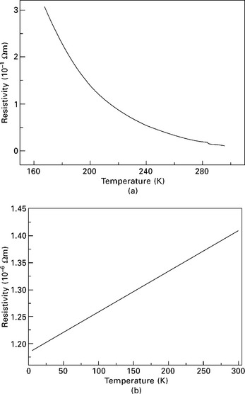
8.6 Temperature dependence of electrical resistivity for a stoichiometric Cu3N sample (a) and for a Cu-rich sample (b).
The host material Cu3N in the cubic anti-ReO3 lattice is a typical semiconductor with an indirect band-gap of ~1.9 eV (Moreno-Armenta et al. 2004, Nosaka et al. 2001, Maruyama and Morishita 1996). Due to the weak Cu–N bonding that facilitates nitrogen re-emission from the compound, the copper nitride samples generally show some deficiency of nitrogen; consequently they display electron-like conductivity as confirmed by the negative Hall coefficient. By careful control of the processing parameters, nearly stoichiometric, single-phased Cu3N thin films can be obtained with a carrier density brought down to below 3.0 × 10¹⁸/cm3.
With the stoichiometrical Cu3N sample at hand, a high-resolution TEM image can be obtained, which requires enormous expertise since the energetic electron beam in a TEM can readily destroy the Cu3N lattice. Figure 8.7 displays the first TEM image for the stoichiometric Cu3N, exhibiting well-aligned {001} fringes, which confirms the high crystallographic quality of the deposit. The planar distance for the {001}-planes, i.e., the lattice constant, measures 0.383 nm in the TEM image, which is in good agreement with the XRD measurements.

Due to the nitrogen deficiency, the deposits consist of distinct nanosized particles instead of being a single crystalline as claimed by some authors. This can be judged easily from the line width of the XRD patterns. From the SEM images (Fig. 8.8) we see that the sample with 76.9% Cu is sharply contrasted, where the size of the crystallites ranges from 40 to 60 nm. For the sample with 75.6% Cu, the crystallites are roughly 40 nm in size, and the image seems smeared. This is obvious since the nearly stoichiometric sample is an insulator – it causes a serious charging effect under the illumination of the electron beam in an SEM.

With the nearly stoichiometrical samples, many inconsistencies concerning the physical properties of Cu3N can be resolved. First, the pure, nearly stoichiometric Cu3N deposit is a typical wide-gap semiconductor, whose electrical resistivity at room temperature measures 2 × 10⁻² Ωm. Smaller values for this quantity originate in the incorporation of Cu particles or Cu-rich {111} surfaces of the Cu3N crystallites. It has a band-gap larger than 1.8 eV, as determined from the photoreflectance spectrum even for the slightly substoichiometric copper nitride thin film with 76.9% Cu (Du et al. 2005). Another important feature is the decomposition temperature. To study the thermal stability of the as-deposited films, the samples were annealed in the same chamber under the nitrogen environment at 0.9 Pa for 20 minutes. in a temperature range from 220 °C to 420 °C. The temperature at which Cu(111) reflection becomes noticeable on the XRD pattern of the post-annealed samples is taken as the decomposition temperature. Aannealing for 20 minutes. at 220 °C and 300 °C does not provoke any discernible changes to the diffraction pattern. Only at 350 °C do two tiny peaks emerge at 2θ ≈ 43.32° and 26 ≈ 50.55° (arrowed in Fig. 8.9) which can be assigned to the (111) and (002) reflections of the pure Cu phase (Fig. 8.9). The primarily absent Cu (111) and (002) reflections unambiguously signify the onset of thermal decomposition of Cu3N. At 420 °C, only strong Cu peaks were observable, the Cu3N completely dissolved. Although from the current experimental data the precise value of the decomposition temperature cannot be fixed, we can say with confidence that the Cu phases emerge from the decomposed stoichiometrical Cu3N, revealed by XRD, only at a temperature of ~350 °C by annealing under the protection of nitrogen at a pressure of 0.9 Pa.

8.3 Nitrogen re-emission
The thermal instability of copper nitrides constitutes essential difficulties for their synthesis and structural characterization. By reactive magnetron sputtering deposition of copper nitride films, the effect of nitrogen re-emission on the film morphology may be directly observable, from which the effect on the growth process and on the microscopic structure of deposits can be inferred. The investigation of this topic is also helpful in understanding the failure mechanism of copper nitrides in usage, which may cause serious instability problems in practical applications.
To demonstrate the effect of nitrogen re-emission, copper nitride thin films were grown with mixed nitrogen (of 60% to 80% in flow rate) and argon as working gas, maintained at a pressure of 1.1–1.3 Pa. The power supply was set at 150 W. Under the given conditions, the deposits are substoichiometric with copper contents exclusively below 77.6%. Under SEM, the films grown for 15 minutes, which are roughly 0.3 μm thick, display a morphology with isolated round blisters (Fig. 8.10). These blisters are typically about 10 microns in dimension. The coverage by these protruding features is about 20%. In films deposited for 30 minutes, the protruding features turned into a ramified rosette-like structure. Such copper nitride rosettes are distributed homogeneously across the sample surface, and show a striking size and shape uniformity, with a lateral dimension around 23 microns (Fig. 8.10). By close inspection of the individual rosettes, it is observed that the rays bifurcate at an average angle of ~74°, slightly larger than the wedge angle of 71.53° for a tetrahedron. In some well-developed ones, fivefold symmetry can be confirmed at the center of the rosettes, though not as strict as in the geometrical sense.

8.10 Effect of nitrogen re-emission on the morphology of copper nitride films. A 0.3 μm thick film exhibits distinct round blisters (a), while in a film grew to ~0.6 μm thick, rosettes with bifurcated rays were observed (b). The rosettes are generally quintilobed, often fivefold symmetry can be identified at the centers.
At first glance, this morphology reminds us of island formation as frequently encountered in growing crystalline films, which can be generally modeled with an atomistic view. But we found that this is not the case. Both the smaller round caps and the larger rosettes are hollow, as confirmed by the presence of some cracked entities. When probing through the crack of a broken rosette, the energy-dispersive X-ray spectrometry detected a dominantly strong signal only for silicon and a weak signal for copper – the nitrogen is completely absent. This is to say that the protruding features are due to a complete local detachment of the film; and in that process some tiny amount of copper is left behind on the Si substrate (Ji et al. 2005, 2006a). Nevertheless, such protruding structures cannot have developed from a previously well-deposited coating due to the accumulated stress. This point can be clarified by briefly examining the necessary area expansion of the material for the formation of such hollow features. As a conservative estimation, consider a round cap 20 μm in lateral dimension and 1 μm high. This corresponds to an area expansion of ~5.0% with regard to the underlying circular base. Such a large area expansion coefficient is prohibitive for rigid materials such as the ionic copper nitride. Moreover, such a morphology is formed in the growth stage, post-growth degradation of an originally flat film due to nitrogen re-emission leaves behind a flat, but Cu-rich surface. The aging of films with a compact morphology in the ambient will not invoke any rosette structure.
The puzzle of the enormously expanded area of the rosettes with regard to the underlying base becomes immediately resolved with the aid of scanning electron micrographs at an enlarged magnification. We see that the deposits with rosette structures are composed of distinct crystallites, around 45 nm in dimension, just like a compact film, but the SEM images taken directly on a rosette reveals the peculiarity in the manner of crystallite stacking. The surface of the rosette structures displays ragged steps and terraces, and it is thinner than the flat portion of the deposits. The typical width of a terrace is about 100 nm (Fig. 8.11). Such a morphology has never been reported, to the best knowledge of the author. We are inspired to speculate that the crystallites in a rosette have experienced a rearrangement process. The area expansion in due course of relief formation is sustained through the gliding of nanocrystals, which is facilitated when the nanocrystals are clothed with the amorphized Cu-terminated {111}-planes; and the ongoing fast growth prevents the film from cracking.

8.11 Scanning electron micrographs at a large magnification of the rosette. Typical crystallite size is 45 nm. The dashed lines are plotted to guide the eye.
In order to fully understand the formation mechanism for such protruding features, we take a close look at the morphological profile of the rosettes. They have the shape of a starfish with rays, but these rays generally do not meet at the same point in the central disk. Occasionally, a symmetrically developed rosette could be found, in which a perfect pentagram is discernible at the center, as shown in Fig. 8.12(a). The rays show further bifurcations, and the offshoots extend generally at an angle of about 74°, a little larger than 72° as required by fivefold rotational symmetry, which in turn is a little larger than the wedge angle of a tetrahedron (α = 70.53°). This cannot be a coincidence, bearing in mind that the tetrahedral crystallites do have the tendency to juxtapose at an angle of about 72° with a [110] orientation in order to fill the space, giving rise to a loosely fivefold symmetry. Fivefold symmetry evolving from this construction mechanism has been confirmed in nanostructures of cubic metals such as Au, Ag and Cu.
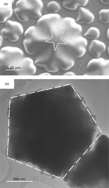
8.12 Fivefoldness in the microstructure of a copper nitride deposit. (a) A rosette displaying perfect fivefold symmetry at the center; (b) a pentagonal assembly of the Cu3N nanocrystals under transmission electron microscope.
As we know, the {111}-planes of the cubic Cu3N lattice comprise exclusively either Cu atoms or N atoms. When nitrogen re-emits from a Cu3N crystallite, it leaves behind crystallites with a soft clothing of amorphous Cu layer in a habit, not necessarily tetrahedral, but with facets joining at the wedge angle (α ≈ 70.53°). The clothing of Cu3N crystallites by Cu {111}-planes also builds a particular electrical conductance path, as verified from the percolation transition in the variation of its electrical resistivity versus the Cu content in the film. When driven by a sufficiently large stress, here initiated by the re-emitted nitrogen gas from beneath, the nanocrystals will undergo a gliding motion against each other along the {111}-planes, and conglomeration of a large quantity of such nanocrystals with facets joining at α ≈ 70.35° results in fivefold symmetry at larger scales. Displayed in Fig. 8.12(b) is a piece of Cu3N crystal in a specimen prepared with mechanical milling for transmission electron microscopic investigation – it is pentagonal with an edge length of 660 nm.
Now the picture becomes clear. An ‘orogenic movement’ model can be formulated to illustrate the formation of relief rosettes in a growing Cu3N thin film (Fig. 8.5). Copper nitride keeps decomposing while film growth proceeds. The re-emitted nitrogen atoms recombine into molecules and together with entrapped nitrogen they agglomerate to form gas bubbles at the film–substrate interface by virtue of a large lateral mobility, since solubility of nitrogen in both Si and Cu3N is low. Adhesion to the local substrate is undermined where a gas bubble forms, and finally detachment occurs (Fig. 8.5(b)). By a delicate balance between expansion via nanocrystal glide and fast growth, the total area and the lateral dimension of the delaminated part grow in pace without cracking. As can be expected, at reduced growth rates a compact morphology of the film ensues. Gliding motion of the crystallites into ragged steps and terraces – similar to the movement of rocks in mountain building, i.e. the orogenic movement – provides the path for a complete strain relaxation; this explains the negligible residual stress in the sample despite the presence of the relief features, as concluded from the transmission electron microscopic and X-ray diffraction data about the lattice constant (Fig. 8.1). The possibility to glide along the Cu-terminated {111}-planes for the pyramidal Cu3N crystallites is prerequisite for the formation of the relief morphology; this also explains its absence in the films of nearly stoichiometrical or heavily Cu-rich samples. As to the quintilobed structure of the rosettes that ramify at a branching-off angle of ~74°, they are the consequence of the preferred packing and rearrangement driven by an anisotropic stress of about two million {111}-faceted Cu3N nanocrystals (Ji et al. 2007). Unlike in the nanorods of cubic metals where the core is fivefold twin crystals textured along the [110]-axis, the fivefold symmetry here is quite ‘soft’ in the sense that it arises rather as an integral effect at large scales.
8.4 Doping of Cu3N by co-sputtering
The structure of Cu3N is, in itself, rather interesting. It is an open structure that can, theoretically, accommodate one more metal ion in each unit cell. The incorporation of an excess metal atom can significantly alter the band structure of the material that continuous semiconducting-to-(semi)metallic transition can be expected, through which various interesting phenomena can be measured in the ternary compounds (Lovett 1977). Here, through the co-sputtering of Cu and Pd targets, we demonstrate the deposition of ternary Cu3NPdx thin films, where a vanishing temperature coefficient of resistivity (TCR) in the range from 240 K down to 5 K could be measured in Cu3NPd0.238 (Ji et al. 2006b). Such a phenomenon has not been found in any other single solids.
The inclusion of another metal atom in each unit cell of the Cu3N lattice results in compounds like Cu4N or the ternary Cu3NPd (Hahn and Weber 1996). Remarkably, Cu3NPd is a semimetal due to the intersection of the energy bands at the Fermi level. Consequently, a semiconducting-to-semimetallic transition is anticipated in the off-stoichiometric Cu3NPdx when ‘x’ increases continuously from zero to unity.
We prepared thin films of Cu3N and Cu3NPdx (0 < x < 0.350) on the Si (001) wafers, a low substrate temperature (~100 °C) in combination with a small power supply (< 150 W) and a high working pressure (> 0.7 Pa) is applied. The interposition of metal atoms at the cell centers of the cubic Cu3N lattice severely deteriorates the covalent bonding in the resulting materials such that the compounds Cu4N and Cu3NPd only exist in theory. In fact, the largest reported value of ‘x’ never exceeds 0.989 in Cu3NPdx whereby the compounds exist in fine powders (Jacobs and Zachwieja 1991). We found that those Cu3NPdx thin film samples with x > 0.5 show a very poor crystallinity; therefore we restrict our discussion to the samples with 0.0 ≤ x ≤ 0.350 which are well crystallized as confirmed by both X-ray diffraction pattern (Fig. 8.13) and transmission electron micrograph (Fig. 8.14). For samples containing only a tiny amount of Pd, e.g., Cu3NPd0.048, the X-ray diffraction pattern remains unchanged, like that of the host Cu3N lattice showing only the (001) and (002) reflections. When the Pd concentration is large enough (x ≥ 0.175), the (001) reflection was replaced by the strong (111) reflection which deteriorates both in intensity and in spectral profile. We can say that the Cu3NPdx thin films here concerned with x < 0.35 are crystalline. The addition of Pd atoms results in a slightly enlarged lattice constant which increases from a = 0.383 nm for the pure Cu3N to a = 0.385 nm for Cu3NPd0.175 (Fig. 8.14). The Cu3NPdx samples obviously have a better electrical conductivity which in turn results in an improved image quality for the transmission electron micrograph (cf. Fig. 8.7). The fact that the Cu3NPdx is metallic at sufficiently large ‘x’ values, while Cu3N is semiconducting, may suggest that the interposition of Pd atoms alter the energy bands near the Fermi surface.


Figure 8.15 displays the temperature dependence of the electrical resisitivty for the nearly stoichiometric Cu3N and for the different ternary Cu3NPdx compounds. Upon cooling from room temperature, the electrical resistivity in the intrinsic Cu3N film rises rapidly (Fig. 8.15(a)). This observation is consistent with the wide band-gap nature of this semiconducting material. The insertion of Pd atoms confers Cu3NPdx an improved electrical conductivity owing to the narrowed band-gap. Even with a tiny amount of Pd insertion as in the samples with x = 0.048 and x = 0.071, the rapid onset of resistivity upon cooling is shifted to below 50 K, indicating a narrowed band-gap for the current samples (Fig. 8.15(b) and (c)). A further addition of Pd atoms initiates the semiconducting-to-semimetallic transition such that the TCR changes its sign. For Cu3NPd0.175, its electrical resistivity rises roughly linearly with decreasing temperature in a range as wide as 270 K, and the TCR is –0.00039 K−1 (Fig. 8.15(d)). Taking T = 280 K as the reference point, the resistance over such a broad temperature range changes only by ~5.0%. The resistivity for Cu3NPd0.349 also displays a good linearity from 50 K to 280 K, but now the TCR is 0.00117 K−1 (Fig. 8.15(f)), indicating unambiguously that now the compound has changed to be metallic. In between these two cases of opposite tendencies for the variation of the electrical resistivity with temperature, we may expect a vanishing TCR over a considerable temperature range at some ‘x’ value. This occurs in the sample Cu3NPd0.238. From 240 K down to 5 K, the TCR is nearly zero (< 3.0 × 10⁻⁶/K), and the relative variance of the electrical resistivity in this temperature range measures as small as 1.42 × 10⁻⁵ (Fig. 8.15(e)).


8.15 Temperature (in K) dependence of the electrical resistivity measured in crystalline Cu3NPdx thin films. (a) x = 0.0; (b) x = 0.048; (c) x = 0.071; (d) x = 0.175; (e) x = 0.238; and (f) x = 0.349. From (b) to (f), the electrical resistivity at room temperature is reduced by four orders of magnitude.
The temperature dependence of the electrical conductivity for solids is susceptible to many influencing factors; no hard-and-fast rules are available. For a semiconductor, the electrical conductivity can be formally written as σ = e(neμe + nhμh), where e and h denote electron and hole, while n and μ stand for the carrier density and carrier mobility, respectively. Both the carrier mobility and the carrier density, or the number of the carriers, are temperature dependent, yet the temperature dependence of the electrical conductivity is dominated by that of the latter, since the mobility changes only in a mild way with the lattice temperature while the number of carriers can be an exponential-like function of 1/T. With decreasing temperature, the number of carriers decreases while the mobility generally increases, but in different manners; consequently, the resulting electrical resistivity is exclusively temperature dependent. For narrow band-gap semiconductors and semimetals, the situation is more complicated than in the conventional semiconductors like Si or Ge. The carrier distribution function obeys the Fermi–Dirac statistics which in this case cannot be approximated by the Maxwell–Boltzmann formula. Moreover, the conduction band is Kane-type that the effective mass of electron, thus the mobility of electron, changes with the carrier density (Lovett 1977). The vanishing TCR occurs when this compound has narrowed its band-gap to be a semimetal for which the temperature dependence of the number of the carriers becomes rather mild-mannered in contrast to the situation in a semiconductor of a definite bandgap. It results from a delicate balance between the opposite changes of the number of carriers and of the carrier mobility with temperature, and reasonably it appears only at temperatures below 240 K – at higher temperatures the increasing number of carriers can easily compensate for the loss in carrier mobility to give rise to a rapidly decreasing electrical resistivity. The current discovery, though lacking a clear scenario of detailed microscopic processes due to the difficulty in calculating the band structure for the off-stoichiometric compounds such as Cu3NPd0.238 and in performing Hall measurement for some supplementary information, does demonstrate the possibility that a balanced change of carrier density and carrier mobility over a wide temperature range is in principle possible in a class of semimetallic materials. Considering the unlikelihood of a temperature-independent electrical resistivity for solids, the current result also bears some significance for solid state physics.
8.5 Conclusions
By carefully adjusting the working parameters including the applied power, gas pressure and the ratio of nitrogen in the working gas, and substrate temperature, thin films of noble-metal nitrides such as Cu3N and Cu3NPdx can be successfully prepared by using the reactive magnetron sputtering method. For stoichiometric Cu3N, the films are found to comprise distinct crystallites in a typical size of 40–60 nm. The peculiarity of growing noble-metal nitride films lies in the fact that the reaction of sputtered metal atoms or clusters with nitrogen occurs most probably only at the target surface, hence the matching of the density and energy of nitrogen ions with the sputtering yield for a chosen target material is the key factor to realizing stoichiometry in the resulting copper nitride films. A large ion energy is unfavorable since the higher sputtering yield of the metal atoms and the weakened combination with energetic nitrogen ions will give rise to a metal-rich deposit. A low substrate temperature is critical since at slightly elevated temperatures nitrogen re-emission occurs, which may even result in microsized protruding features. Semiconducting to (semi)metallic transition can be observed in doped Cu3N structures wherein the excessive atoms are expected to sit at the cell centers of the Cu3N lattice. A vanishing temperature coefficient of resistivity over a temperature of 200 K has been realized in Cu3NPd0.238. Many other surprising properties are anticipated in the noble-metal nitrides, which await discovery in the future.
8.6 References
Asano, M., Umeda, K., Tasaki, A. Cu3N thin film for a new light recording media. Jpn. J. Appl. Phys.. 1990; 29:1985–1986.
Baranov, O., Romanov, M., Wolter, M., Kumar, S., Zhong, X.X., Ostrikov, K. Low-pressure planar magnetron discharge for surface deposition and nanofabrication. Physics of Plasma. 17, 2010. [053509].
Berg, S., Nyberg, T. Fundamental understanding and modeling of reactive sputtering processes. Thin Solid Films. 2005; 476:215–230.
Borsa, D.M., Grachev, S., Presura, C., Boerma, D.O. Growth and properties of Cu3N films and Cu3N/γ-Fe4N bilayers. Appl. Phys. Lett.. 2002; 80:1823–1825.
Cao, Z.X. Electron cyclotron waveresonance plasma assisted deposition of cubic boron nitride thin films. J. Vac. Sci. Technol. A. 2001; 19:485–489.
Cao, Z.X. Plasma enhanced deposition of silicon carbonitride films and property characterization, Diamond & Relat. Mater.. 2002; 11:16–21.
Cao, Z.X., Oechsner, H. Effect of concurrent N2+ -ion bombardment on the physical vapor deposition of nitrides thin films. J. Vac. Sci. Technol. A. 2004; 22(2):321–323.
Chambers, S.A. Epitaxial growth and properties of doped transition metal and complex oxide films, Adv. Mater.. 2010; 22(2):219–248.
Cremer, R., Witthaut, M., Neuschutz, D., Trappe, C., Laurenzis, M., Winkle, O., Kurz, H. Deposition and characterization of metastable Cu3N layers for applications in optical data storage. Mikro. Acta.. 2000; 133:299–302.
Dorranian, D., Dejam, L., Sari, A.H., Hojabri, A. Structural and optical properties of copper nitride thin films in a reactive Ar/N2 magnetron sputtering system. Euro. Phys. J.-Appl. Phys. 50, 2010. [20503.].
Du, Y., Ji, A.L., Ma, L.B., Wang, Y.Q., Cao, Z.X. Electrical conductivity and photoreflectance of nanocrystalline copper nitride thin films deposited at low temperature, J. Crystal Growth. 2005; 280:490–494.
Hahn, U., Weber, W. Electronic structure and chemical-bonding mechanism of Cu3N, Cui3NPd, and related Cu(I) compounds. Phys. Rev. B. 1996; 53:12684–12693.
Hojabri, A., Haghighian, N., Yasserian, K., Ghoranneviss, M. The effect of nitrogen plasma on copper thin film deposited by DC magnetron sputtering. IOP Conf. Ser.: Mater. Sci. Eng. 12, 2010. [012004].
Jacobs, H., Zachwieja, U. Kupferpalladiumnitride, Cu3PdxN mit x = 0.020 und 0.989, Perowskite mit ‘bindender 3d10-4d10-Wechselwirkung’. J. Less-common Met. 1991; 170:185–190.
Ji, A.L., Li, C.R., Du, Y., Ma, L.B., Song, R., Cao, Z.X. Formation of rosette pattern in copper nitride thin films via nanocrystals gliding. Nanotech. 2005; 16:2092–2095.
Ji, A.L., Huang, R., Du, Y., Li, C.R., Cao, Z.X. Growth of stoichiometric Cu3N thin films by reactive magnetron sputtering. J. Crystal. Growth. 2006; 295:79–83.
Ji, A.L., Li, C.R., Cao, Z.X. Ternary Cu3NPdx exhibiting invariant electrical resisitivity over 200 K. Appl. Phys. Lett.. 89, 2006. [252120].
Ji, A.L., Du, Y., Li, C.R., Cao, Z.X. Formation of symmetrical relief features in nanocrystalline copper nitride thin films. J. Vac. Sci. Technol. B. 2007; 25(1):208–211.
Juza, R., Hahn, H. Copper nitride (in German). Z. Anorg. Allg. Chem.. 1939; 241:172–178.
Kim, K.J., Kim, J.H., Kang, J.H. Structural and optical characterization of Cu3N films prepared by reactive RF magnetron sputtering. J. Crystal Growth. 2001; 222:767–772.
Lovett, D.R. Semimetals & Narrow-bandgap Semiconductors. London: Pion Limited; 1977.
Ma, G.M., Alejandro, M., Noboru, T. Ab initio total energy calculations of copper nitride: the effect of lattice parameters and Cu content in the electronic properties. Solid Stat Sci.. 2004; 6:9–14.
Maruyama, T., Morishita, T. Copper nitride and tin nitride thin films for write- once optical recording media. Appl. Phys. Lett.. 1996; 69:890–891.
Moreno-Armenta, M.G., Martínez-Ruiz, A., Takeuchi, N. Ab initio total energy calculations of copper nitride: the effect of lattice parameters and Cu content in the electronic properties. Solid State Sciences. 2004; 6:9–14.
Musil, J., Baroch, P., Vlcek, J., Nam, K.H., Han, J.G. Reactive magnetron sputtering of thin films: present status and trends. Thin Solid Films. 2005; 475:208–218.
Norskov, J.K., Hammer, B. Why gold is the noblest of all the metals. Nature. 1995; 376:238–240.
Nosaka, T., Yoshitake, M., Okamoto, A., Ogawa, S., Nakayama, Y. Thermal decomposition of copper nitride thin films and dots formation by electron beam writing. Appl. Surf. Sci.. 2001; 169–170:358–361.
Reddy, K.V.S., Reddy, A.S., Reddy, P.S., Uthanna, S. Copper nitride films deposited by dc reactive magnetron sputtering. J. Mater. Sci.– Materials in Electronics. 2007; 18:1003–1008.
Terada, S., Tanaka, H., Kubota, K. Heteroepitaxial growth of Cu3N thin films. J Crystal Growth. 1989; 94:567–568.
Wang, D.Y., Nakamine, N., Hayashi, Y. Properties of various sputter-deposited Cu–N thin films. J. Vac. Sci. Technol. A. 1998; 16:2084–2092.