
Measuring nucleation and growth processes in thin films
Abstract:
This chapter focuses on the observation of crystal growth processes by tracking the motion of atomic steps, which are the growth front of the crystal. After reviewing the theoretical model for atomic step motion, the chapter discusses atomic step imaging by scanning electron microscopy, and reveals basic growth modes using this technique: two-dimensional-island nucleation and step-flow modes both in growth and evaporation, and morphological instability of atomic steps between these two modes.
1.1 Introduction
Recent progress in surface observation techniques has enabled crystal surfaces to be observed at the atomic scale. In particular, with scanning tunnelling microscopy (STM) (Binnig and Rohrer, 1983), the motion of individual atoms on the surface can be tracked (Swartzentruber, 1996). However, at high temperatures where crystal growth takes place, atoms diffuse on the surface so fast that any existing methods cannot catch up with their movements. In vapour phase growth, those diffusing atoms, termed adatoms, finally evaporate or meet an atomic step where they are incorporated into the crystal. By the incorporation of adatoms, the motion of atomic steps takes place. The motion of atomic steps is much slower than that of adatoms. Furthermore, atomic resolution is not necessary for the observation of atomic steps which have a one-dimensional structure on the surface. Therefore, we are able to observe the crystal growth processes by tracking the motion of atomic steps which constitute the growth front of the crystal. For this purpose, electron microscopy techniques with a high sensitivity to atomic steps are useful: these include reflection electron microscopy (REM) (Osakabe et al., 1980) and low energy electron microscopy (LEEM) (Bauer, 1994). These two techniques utilize electron diffraction from the surface, and thus are sensitive to the surface morphology at atomic steps.
In this chapter, however, we use a different electron microscopy, scanning electron microscopy (SEM), to observe the motion of atomic steps. As the growth method, we focus on the molecular beam epitaxy (MBE), where the crystal surface in a vacuum is exposed to a molecular flux of evaporated source material. Before explaining the principle of atomic step imaging by SEM, we review the theoretical description of atomic step motion. The theoretical model was established in 1951 by Burton, Cabrera and Frank (BCF model) (Burton et al., 1951). Interestingly, this is far earlier than the establishment of MBE and surface characterization techniques.
1.2 Basic theory of epitaxial growth
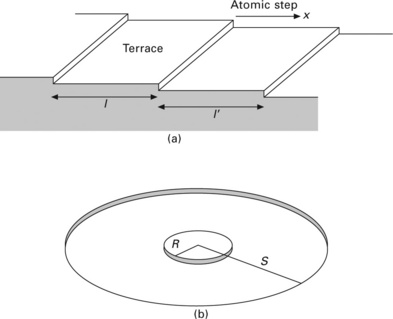
We consider step-flow growth on a vicinal surface with parallel atomic steps. We take the x-axis perpendicular to the atomic steps as shown in Fig. 1.1(a). Atoms supplied from a molecular beam are adsorbed and migrate freely on the surface (adatoms). The time evolution of adatom density, ρ(x,t), is described by the following diffusion equation:
where Ds is the diffusion coefficient of adatoms, F is the flux of impinging atoms, 1/τv is the evaporation probability of an adatom. The first term on the right-hand side in Eq. 1.1 represents the diffusion of adatoms, the second term represents the loss by evaporation, and the third term is the increment due to deposition. F is expressed by using the partial pressure, p, of the molecule composed of η atoms usable for growth:
where kB is the Boltzmann constant, m is the mass of the molecule, and T is the absolute temperature.
To solve Eq. 1.1, we assume that the rate of attachment and detachment of adatoms at the steps is much faster than that of diffusion. That is, the adatom density at the step becomes an equilibrium value ρ0. When the surface diffusion is much faster than the motion of steps, ![]() . Then, for an isolated step at x = 0, the boundary conditions are ρ(0) = ρ0, ρ(∞) = Fτv. These give the following solution
. Then, for an isolated step at x = 0, the boundary conditions are ρ(0) = ρ0, ρ(∞) = Fτv. These give the following solution
where λs2 = Dsτv, and λs is the surface diffusion length of adatoms. The step velocity v is determined by the adatom flux at the step
For an isolated step, assuming the fluxes from upper and lower terraces are equal (symmetric),
where n0 = a− 2 is the density of lattice (lattice constant a) on the surface. The step velocity is proportional to 2λs. This means that only atoms impinging within λs from the step contribute to the step motion, and other atoms evaporate before reaching the step. This growth mode occurs when the diffusion length is much smaller than the step spacing. For the opposite case, when the diffusion length is much larger than the step spacing:
where l and l′ are the widths of upper and lower terraces, respectively.
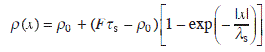
For circular steps, we need to solve the diffusion equation in the cylindrical coordinates. The general solution is expressed as
where K0 and I0 are the modified Bessel functions of order zero, and A and B are the proportional constants. For the circular step between an inner terrace of radius R on a larger terrace of radius S as shown in Fig. 1.1(b),
where KX = K0 (X/λs), IX = I0(X/λs). The step velocity is obtained as the sum of the adatom fluxes from inner and outer terraces:
where K1X = K1(X/λs), and I1X = I1(X/λs) are the modified Bessel functions of order 1 (Finnie and Homma, 2000b).
1.3 Observation method of atomic steps
For the observation of atomic steps on growing surfaces, we employed in-situ SEM. Atomic steps can be observed with a conventional SEM instrument, but the contrast is so faint that it is easily hidden by the contamination of the surface due to electron irradiation during SEM imaging. We used an ultrahigh vacuum SEM instrument equipped with Knudsen cells for molecular beam epitaxy (Homma et al., 1994). The secondary electron detector was set to the side of the specimen in parallel to the axis of the specimen stage tilting. The primary electron beam of 25 keV was incident at a grazing incidence, 5–30° to the surface, to enhance the sensitivity to the atomic scale surface structures. In this article, the primary electron beam was incident from the bottom direction of each image. The image foreshortening due to oblique incidence is corrected in most images. The atomic steps appear bright when the primary electron beam goes down the atomic step staircase, while they appear dark when the primary electron beam goes up the staircase (Homma et al., 1991). Another factor influencing the atomic step contrast is the location of the secondary electron detector (Homma et al., 1993b). When the primary electron beam goes parallel to the atomic steps, the atomic steps appear bright when the steps are facing the detector. Conversely, they appear dark when they face away from the detector. Those are topographic contrasts of atomic steps, which are similar to macroscopic scale step contrasts, and can be used for imaging of steps as small as the monatomic layer of the crystal. This observation method is used in Section 1.4.
An entirely different type of contrast can be used for atomic step imaging. This is the surface phase contrast utilizing surface phase transition. In the following, we explain the 7 × 7 − 1 × 1 contrast on Si(111) surfaces.
A clean Si(111) surface in ultrahigh vacuum takes a long range ordered structure, the 7 × 7 reconstruction, at below the transition temperature (~860 °C) (Florio and Robertson, 1970). The 7 × 7 reconstruction starts to occur at the atomic step edge during cooling from a high temperature. In SEM images, a 7 × 7 domain appears brighter than a 1 × 1 domain without reconstruction (Homma et al., 1993a). Therefore, if 7 × 7 domains form continuously along an atomic step, the step is easily observed by SEM even with a low magnification. One such method is to keep the sample 1–2 °C below the transition temperature, and observe thin 7 × 7 domains along atomic steps. Another method is to rapidly quench the sample from above the transition temperature towards room temperature, thus forming continuous 7 × 7 domains along atomic steps.
The image in Fig. 1.2 was observed using the former method. Using a Si(111) wafer with a small miscut angle, 0.01°, the sample was kept 1 °C below the transition temperature. The 1 × 1 − 7 × 7 phase transition starts from the upper edge of an atomic step, and only a thin region of the upper terrace becomes 7 × 7 and appears bright. Since the width of continuous 7 × 7 regions is negligible to the large step spacing, 1.5 μm, the atomic steps are highlighted in the image. This method can be used for the observation of atomic step behaviour not only at around the phase transition temperature but also at higher temperatures by reducing the temperature just for observation purposes.
1.2 SEM image of atomic steps on Si(111) surface observed at the 1 × 1 − 7 × 7 phase transition temperature. Atomic steps are decorated with continuous 7 × 7 regions which appear bright in the SEM image.
An example of the quenching method is shown in Fig. 1.3 (Homma and Finnie, 2002). The Si sample with a flat terrace as large as a 100 μm square was rapidly quenched from 1230 °C (see Section 1.5). Concentric atomic steps with a spacing of ~20 μm can be seen. In between the concentric steps there exist smaller circular steps. Those are monolayer holes on the annular terraces. A magnified image of the small circular step is shown in Fig. 1.3(b). The lower half of the atomic step appears bright, while the upper half appears dark. This contrast change is due to the difference in the primary electron incidence relative to the atomic step edge, as explained above. The topographic effect alone produces the atomic step image in SEM, but the contrast is not high enough to be recognized in a low magnification image.
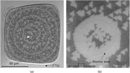
1.3 SEM image of atomic steps on Si(111) surface observed by the quenching method (Homma and Finnie, 2002). Bright regions are 7 × 7 reconstructed domains. (a) Low magnification image. (b) High magnification image observed at the arrow head shown in (a).
Both the upper and lower terraces near an atomic step turn to the 7 × 7 phase after quenching. The width of the 7 × 7 phase on the upper terrace (outside of the hole) is 0.3–0.4 μm, and that on the lower terrace (inside of the hole) is roughly twice as large. Therefore, the atomic step is observed as a ~1 μm wide line. Meanwhile, many triangular 7 × 7 domains can be seen on the terrace in the image shown in Fig. 1.3(b). Since these triangular domains distribute discretely, only atomic steps continuously decorated by 7 × 7 domains are highlighted in the low magnification image shown in Fig. 1.3(a).
In Sections 1.5 and 1.6, we discuss the atomic step behaviour on Si(111) surfaces at high temperatures based on observations using the quenching method. Although it is not a real-time observation method, the effect of quenching on the step motion is negligible because phenomena occurring on a large scale are observed on a huge terrace. It is interesting that macroscopic observations by SEM in the 10–100 μm range can reveal phenomena which relate to the attachment and detachment of atoms to/from atomic steps.
1.4 Two-dimensional-island nucleation and step-flow growth modes
In MBE growth, two basic growth modes exist depending on the ratio of the adatom diffusion length and the terrace width: the step-flow growth mode where growth proceeds through atomic step progression, and two-dimensional (2D) island nucleation growth mode where growth proceeds through island coverage increase. Here, we show those two growth modes on GaAs surfaces observed by SEM.
On a GaAs(001) surface, a monolayer step consists of Ga and As double layers with a height of 0.28 nm. In Fig. 1.4, the process of one monolayer evolution of a GaAs(001) surface is shown using the characteristic of scanning imaging (Homma et al., 1995): acquisition of one image takes a certain period while growth proceeds during the period. In the present case, the image acquisition time and the monolayer growth period are 70 s and 50–55 s, respectively. Therefore, ~1.3 monolayers grow during one frame imaging, and the process can be recorded in the image. Note that the growth stage differs from the top to the bottom of the image. Growth started at the beginning of imaging (at the top of the image). Initially, atomic steps are visible. Then, small spots appear at about a quarter from the top. These are 2D islands nucleating on the surface. Then, the islands grow rapidly in a lateral direction, causing coalescence of the islands. At three-quarters from the top, holes are seen as the result of island coalescence, and finally one monolayer is completed. Atomic steps can be recognized at around the completion of one monolayer. The second layer islands appear in the bottom part of the image. In this way, an SEM image can record the growth of one monolayer in real time for the 2D island nucleation growth mode. In the initial period of one monolayer growth, islands are not observed. This is not due to the resolution of SEM, but reflects the surface reconstruction process of GaAs(001) surface. In the 2 × 4 structure, which is observed before MBE growth, As atoms corresponding to quarter monolayer growth are lacking, thus Ga atom rearrangement is necessary before island nucleation can occur (Osaka et al., 1995).
1.4 SEM image of GaAs (001) surface during MBE growth (Homma et al., 1995). Growth started at the top of the image and one monolayer growth is completed at about three-quarters of the image length from the top.
The reason for the use of a slow growth rate is to make the islands large. The island size also relates to the surface diffusion length of adatoms. Thus, the Ga-stabilized GaAs(111) surface (so-called (111)A surface), where the surface diffusion length is much larger than that on the (001) surface, was employed. The island growth process on this surface is shown in Fig. 1.5 (Yamaguchi and Homma, 1998). In this case, a higher image acquisition time was used and the same area of the surface was repeatedly observed during growth. owing to the large island size, nucleation, growth and coalescence processes are clearly seen in Fig. 1.5. The islands are triangular, reflecting the three-fold symmetry of the (111) surface. Furthermore, step-flow growth occurs without nucleation of island near the step edge. The step velocity is higher parallel to the original steps than that in the perpendicular direction. Precise analyses of the step velocity under different Ga supplying rate showed that the step velocity was well described by Eq. 1.2 for an isolated step. This is because the step spacing is much larger than the Ga diffusion length on the GaAs(111)A surface. Fitting the measured step velocity dependence on the Ga flux gave the Ga diffusion length of ~100 nm. Note that the step spacing is more than 1 mm on the surface.
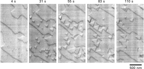
1.5 SEM image sequences showing the monolayer growth process of GaAs(111)A surface (Yamaguchi and Homma, 1998). Each image corresponding to 8 s growth starting from the time shown at the top.
1.5 The motion of atomic steps on a growing and evaporating Si(111) surface
Here, we consider the atomic step motion during evaporation at high temperatures on the surface with an atomic step array with regular intervals as shown in Fig. 1.6. A mathematical expression for this is given in the Appendix. on the high temperature surface, adatoms are released from an atomic step and migrate freely onto the terrace. An atomic step acts as an emitter and a sink of adatoms simultaneously, and thus the adatom concentration at the atomic step reaches an equilibrium value. In the case of evaporation, the adatom concentration at the middle of a terrace decreases due to desorption. Adatoms are supplied from the atomic step for compensation of the decrease, causing retraction motion of the atomic step. This is the step-flow evaporation. Adatoms can also be created directly on the middle of a terrace, though the probability is small. In this case, an adatom and an advacancy are created simultaneously. An advacancy can be annihilated by recombination with an adatom. Advacancies diffuse much more slowly than adatoms, because an advacancy consists of surrounding surface atoms. When the terrace size is large enough, the advacancy concentration at the centre of the terrace increases to the extent that advacancies form 2D holes at the centre of the terrace. This is the counterpart of the 2D island nucleation in growth. Usually, only step-flow evaporation is observed on Si(111) surfaces, because the diffusion length for adatoms is much larger than the atomic step spacing on normal substrates.
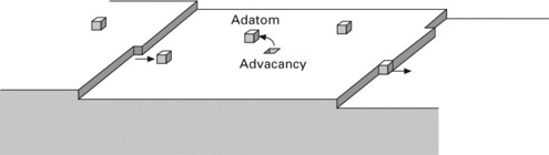
1.6 Schematic illustration of adatoms and advacancies on the high temperature surface with atomic step allay.
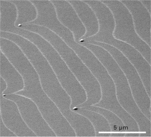
In the meantime, we consider a crater (hole) on a crystalline surface as illustrated in Fig. 1.7. In the crater, there exists a slope whose inclination direction is opposite to the average inclination of the surface, i.e., the step-flow direction is opposite to the average surface. Therefore, the very bottom terrace of the crater expands during step-flow evaporation (Homma et al., 1997). When the bottom terrace becomes large enough, a new terrace appears due to 2D-macro-vacancy nucleation in the centre of the terrace. The lower terrace expands in the same way as the initial terrace, and the macro-vacancy nucleation is repeated. As a result, a set of concentric circular steps is created at the bottom of the crater as shown in Fig. 1.8. The spacing of the circular steps is on the order of adatom diffusion length (see Section 1.9.2), and thus varies with the temperature. Figure 1.9 shows the temperature dependence of the atomic step spacing observed using a huge crater created on a Si(111) surface by oxygen-ion bombardment in a secondary-ion mass spectrometer (Homma et al., 1998).
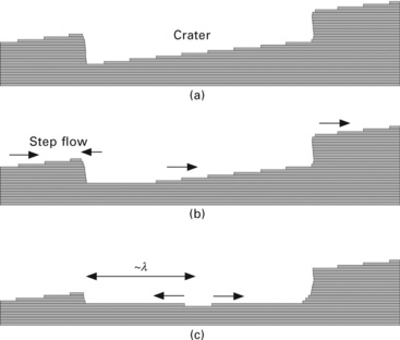
1.7 Schematic illustration of step-flow evaporation of the surface with a crater. (a) Initial surface. (b) Step-flow directions in the crater during evaporation. (c) Macro-vacancy formation after the bottom terrace size exceeds the adatom diffusion length.
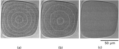
1.8 SEM images of circular atomic steps on ultra-large terrace at the bottom of a crater on Si(111) surface. The annealing temperature before quenching is (a) 1180 °C, (b) 1120 °C and (c) 1020 °C. No macro-vacancy formation occurred in (c).
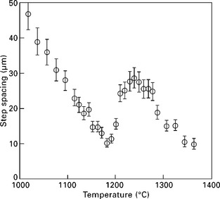
1.9 Temperature dependence of atomic step spacing observed on ultra-large terraces formed at the bottom of a crater on Si(111) surface (Homma et al., 1998).
The step spacing decreases with increasing temperature up to 1200 °C. This relates to the decrease in the surface diffusion length caused by the increase in the desorption probability of adatoms: the surface diffusion coefficient Ds is given by
where a is the lattice constant, υ0 is the frequency factor (~1013), Wsd is the energy barrier of surface diffusion, and T is the absolute temperature. The desorption probability of adatoms is expressed using the desorption barrier Wv as
Using Einstein’s formula λs2 = Dsτv, we get
The slope in the range of 1000–1200 °C in Fig. 1.9 gives Wv − Wsd ≈ 2.4 eV.
The step spacing suddenly increases by a factor of 2.6 at around 1200 °C, and decreases again for higher temperatures. This sudden increase suggests occurrence of some transition on the surface. In fact, incomplete surface melting, which is disordering of the first layer in the double layers of the Si(111) surface, has been observed by medium-energy ion scattering spectroscopy at this temperature (Hibino et al., 1998). The surface structure transition may affect the surface diffusion of adatoms. Actually, the image shown in Fig. 1.3 is the surface formed by quenching from 1230 °C. Small circles are seen between concentric atomic steps. These are monolayer holes located at the middle of the annular terrace between the adjacent concentric steps. When the sample passed through the transition temperature during cooling, the adatom diffusion length suddenly decreased. This caused nucleation of advacancy islands (monolayer holes) at the centre of the terrace as explained above.
By varying the annealing temperature, the spacing of the concentric atomic steps can be changed in the range 10–50 μm. If the annealing temperature is set so that the step spacing is less than half of the bottom terrace size, no nucleation of new islands occurs. Thus, an ultra-large terrace without atomic steps inside can be obtained as shown in Fig. 1.8(c) (Finnie and Homma, 2000a).
By using the ultra-large terrace created at the bottom of a crater, we can create a monolayer island or hole by growth or evaporation. With the combination of island or hole, and growth or evaporation, we can observe four cases as shown in Fig. 1.10: island shrinkage and hole expansion during evaporation; island expansion and hole shrinkage during growth. As an example, analysis of evolution of circular terraces during growth and evaporation at 940 °C is shown in Fig. 1.11 (Finnie and Homma, 2000b; Homma and Finnie, 2002). The time evolution of the circular island and hole can be described by that of their radii. Experimentally obtained step velocities were well fitted to the solution of the BCF equation on the cylindrical coordinate (Eq. 1.4). The surface diffusion length of adatoms at 880 °C estimated from the fitting was ~50 μm, which is in good agreement with the step spacing in Fig. 1.9.
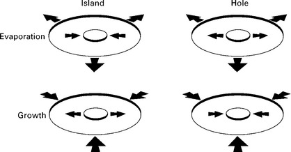
1.10 Schematic illustration of step-flow growth and evaporation of monolayer island and hole on a circular terrace.
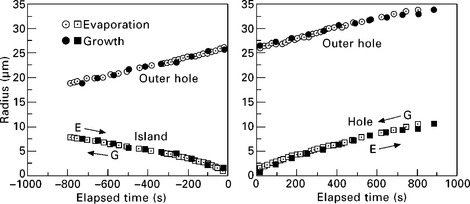
1.11 The radii of circular terraces as a function of annealing or growth time observed at 940 °C on the ultra large Si(111) terrace (Homma and Finnie, 2002). The data for evaporation are overlaid with those for growth by expanding the timescale of growth by a factor of two. The time axis of growth is reversed to facilitate comparison. Arrows indicate the direction of radius change during evaporation (E) and growth (G).
As seen in Fig. 1.11, the step progression and retraction are symmetric. Also, the behaviours of hole and island are symmetric. These indicate that the contributions of upper and lower terraces are symmetric when adatoms are incorporated into or released from atomic steps. In general, adatoms from the upper terrace need to cross a higher energy barrier to be incorporated into atomic steps than those from the lower terrace. This is called the Ehrlich–Schwoebel barrier (Ehrlich and Hudda, 1966, Schwoebel and Shipsey, 1966). The present results indicate that the Ehrlich–Schwoebel barrier is not significant for the Si(111) surface at high temperatures.
1.6 Morphological instability of atomic steps
The Ehrlich–Schwoebel barrier is asymmetry in incorporating adatoms into a step between those from the upper and lower terraces. Such asymmetry can cause instability in step flow. Bales and Zangwill (1990) treated theoretically the wandering of steps in step-flow growth and showed that when the flux of adatoms from the lower terrace exceeds that from the upper terrace, the fluctuation in the atomic step is amplified, resulting in macro-scale step wandering. This unstable growth regime is located between stable step flow and 2D island nucleation in the phase diagram of growth mode as functions of impinging flux and step spacing.
As discussed above, the Ehrlich–Schwoebel barrier on the Si(111) surface at high temperatures is small and this kind of step wandering is not observed. Here, we show step instability in a different way. We utilized the fact that the adatom flux to atomic step is an increasing function of the terrace width, and distorted the symmetry between the upper and lower terraces by changing the ratio of their sizes (Finnie and Homma, 2000c). This is possible only by using an ultra-large terrace such as shown in Fig. 1.8(c).
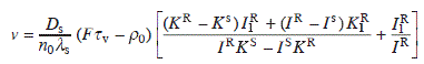
Figure 1.12 shows the time evolution of atomic step shape on a 100 μm wide terrace (Homma et al., 2001). The observation was carried out using a low Si molecular flux for nucleating only an island at the centre of the terrace at 880 °C. Each frame was observed by the quenching method after growth duration starting from the flat surface. This was to avoid any extra nucleation due to repeated quenching. A small circular island is seen at the centre of the terrace in image (a). This changes to the six-fold symmetry island extending in < 110 > directions as seen in images (b) and (c). In this stage, the peripheral atomic step progressing from the edge of the terrace is smooth. After further growth, the periphery step becomes wandering as seen in image (d). The wandering amplitude maximizes at 0.5 monolayers, and then decreases for further growth as in image (e). The decay of wandering is due to the stabilization of step flow when the upper terrace becomes large.
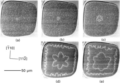
1.12 SEM image sequences showing the evolution of atomic step instability during growth at 880 °C on the ultra large Si(111) terrace (Homma et al., 2001). The images were obtained after growth of (a) 10 s, (b) 20 s, (c) 1 min, (d) 5 min and (e) 10 min.
While the shape of the centre island reflected the symmetry of the Si(111) surface, the periphery step was initially smooth and became wandering afterwards. This is exactly the result of step fluctuation enhancement by the large lower terrace.
1.7 Conclusion and future trends
This chapter has shown that crystal growth of Si and GaAs in molecular beam epitaxy is well described by the BCF model. That is, the surface diffusion of adatoms is the dominant process of crystal growth and the incorporation of adatoms into atomic steps is fast enough. On the evaporating surface, the behaviour of advacancies is also well described by the BCF model. The key to observe the atomic step motion of growing and evaporating Si surface at high temperatures is the use of an ultra-large terrace created at the bottom of a crater. Since the surface diffusion length of adatoms on a Si(111) surface at high temperature becomes as large as 10–50 μm, a terrace width comparable to the surface diffusion length is a prerequisite. SEM imaging with the quenching method is useful for such a large-scale observation. In this method, atomic steps were decorated with the 7 × 7 phase domains. In order to obtain an enhanced 7 × 7 domain contrast, an oblique incidence of a 25 keV primary electron beam was used. Recent progress in electron microscopy has made it easier to observe atomic steps. A low energy SEM instrument with a primary electron beam of 0.1–1 keV is commercially available these days. Surface sensitivity is largely enhanced with the low energy beam, especially when it is used in an ultrahigh vacuum. Low energy electron microscopy (LEEM), which uses projection optics of reflected electrons for imaging, has realized real-time imaging of atomic steps even at elevated temperatures. LEEM is now widely used for observation of growing surfaces of various materials (Bauer, 1994; Meyer zu Heringdorf, 2008).
1.8 References
Bales, G.S., Zangwill, A. Morphological instability of a terrace edge during step-flow growth. Phys. Rev. B. 1990; 41:5500–5508.
Bauer, E. Low energy electron microscopy. Rep. Prog. Phys.. 1994; 57:895–938.
Binnig, G., Rohrer, H. 7 × 7 reconstruction on Si(111) resolved in real space. Phys. Rev. Lett.. 1983; 50:120–123.
Burton, W.K., Cabrera, N., Frank, F.C. The growth of crystals and the equilibrium structure of their surface. Phil. Trans. Roy. Soc.. 1951; 243:299–358.
Ehrlich, G., Hudda, F.G. Atomic view of surface self-diffusion: tungsten on tungsten. J. Chem. Phys.. 1966; 44:1039–1049.
Finnie, P., Homma, Y. Motion of atomic steps on ultraflat Si(111): constructive collisions. J. Vac. Sci. Technol.. 2000; A18:1941–1945.
Finnie, P., Homma, Y. Nucleation and step flow on ultraflat silicon. Phys. Rev. B. 2000; 62:8313–8317.
Finnie, P., Homma, Y. Stability–instability transitions in silicon crystal growth. Phys. Rev. Lett.. 2000; 85:3237–3240.
Florio, J.V., Robertson, W.D. Phase transformations of the Si(111) surface. Surf. Sci.. 1970; 22:459–464.
Hibino, H., Sumitomo, K., Fukuda, T., Homma, Y., Ogino, T. Disordering of Si(111) at high temperatures. Phys. Rev. B. 1998; 58:12587–12589.
Homma, Y., Finnie, P. Step dynamics on growing silicon surfaces observed by ultrahigh vacuum scanning electron microscopy. J. Cryst. Growth. 2002; 237–239:28–34.
Homma, Y., Tomita, M., Hayashi, T. Secondary electron imaging of monolayer steps on a clean Si(111) surface. Surf. Sci.. 1991; 258:147–152.
Homma, Y., Suzuki, M., Tomita, M. Atomic configuration dependent secondary electron emission from reconstructed silicon surfaces. Appl. Phys. Lett.. 1993; 62:3276–3278.
Homma, Y., Tomita, M., Hayashi, T. Atomic step imaging on silicon surfaces by scanning electron microscopy. Ultramicroscopy. 1993; 52:187–192.
Homma, Y., Osaka, J., Inoue, N. In-situ observation of monolayer steps during molecular beam epitaxy of gallium arsenide by scanning electron microscopy. Jpn. J. Appl. Phys.. 1994; 33:L563–L566.
Homma, Y., Osaka, J., Inoue, N. In situ observation of surface morphology evolution corresponding to reflection high energy electron diffraction. Jpn. J. Appl. Phys.. 1995; 34:L1187–L1190.
Homma, Y., Hibino, H., Ogino, T., Aizawa, N. Sublimation of Si(111) surface in ultrahigh vacuum. Phys. Rev. B. 1997; 55:R10237–R10240.
Homma, Y., Hibino, H., Ogino, T., Aizawa, N. Sublimation of a heavily borondoped Si(111) surface. Phys. Rev. B. 1998; 58:13146–13150.
Homma, Y., Finnie, P., Uwaha, M. Morphological instability of atomic steps observed on Si(111) surfaces. Surf. Sci.. 2001; 492:125–136.
Meyer, zu, Heringdorf, F.-J. The application of low energy electron microscopy and photoemission electron microscopy to organic thin films. J. Phys.: Condens. 2008; 20:184007-1–184007-12.
Osaka, J., Inoue, N., Homma, Y. Delayed and continuous nucleation of islands in GaAs molecular beam epitaxy revealed by in situ scanning electron microscopy. Appl. Phys. Lett.. 1995; 66:2110–2112.
Osakabe, N., Tanishiro, Y., Yagi, K., Honjo, G. Reflection electron microscopy of clean and gold deposited (111) silicon surfaces. Surf. Sci.. 1980; 97:393–408.
Pimpinelli, A., Villain, J. What does an evaporating surface look like? Physica A. 1994; 204:521–524.
Schwoebel, R.L., Shipsey, E.J. Step motion on crystal surfaces. J. Appl. Phys.. 1966; 37:3682–3686.
Swartzentruber, B.S. Direct measurement of surface diffusion using atom-tracking scanning tunneling microscopy. Phys. Rev. Lett.. 1996; 76:459–462.
Yamaguchi, H., Homma, Y. Imaging of layer by layer growth processes during molecular beam epitaxy of GaAs on (111)A substrates by scanning electron microscopy. Appl. Phys. Lett.. 1998; 73:3079–3081.
1.9 Appendix
1.9.1 Extension of the Burton, Cabrera & Frank (BCF) model for evaporating surface
This appendix discusses the behaviour of adatoms and advacancies on an evaporating surface following the work by Pimpinelli and Villain (1994).
At high temperatures not far from the melting point, advacancies as well as adatoms exist on the surface. We need to take advacancies into account when we discuss the problems relating to evaporation on the surface. The concentration of advacancy σ(x) on the terrace has a minimum at the centre of the terrace opposite to the concentration distribution of adatoms. When the concentration of advacancy exceeds a certain value, a macro-vacancy, one monolayer deep hole, is created.
To treat both advacancies and adatoms, we need to consider their pair creation and pair annihilation. The annihilation rate of an adatom-advacancy pair is proportional to the product of their concentrations, ρσ. The pair creation rate at equilibrium is proportional to their equilibrium concentration, ρ0σ0. These values satisfy the coupled equations
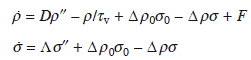
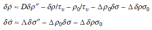
where D and Λ are the diffusion coefficients of adatoms and advacancies, respectively, and Δ is the proportional constant. To linearize the equations, we introduce δρ = ρ − ρ0 and δσ = σ − σ0, and suppose these are small (near equilibrium). Also, we neglect the external flux F. Then, we get
Since the step motion is much slower than the diffusion of adatoms and advacancies, ![]() and
and ![]() . Under the boundary conditions, ρ (± l/2) = ρ0, σ(± l/2) = σ0, we get
. Under the boundary conditions, ρ (± l/2) = ρ0, σ(± l/2) = σ0, we get
In general, since adatoms diffuse much faster than advacancies, Dρ0 > > Λσ0, then, 1/κ2 ≈ Dτv = λ2.
The step velocity for equidistant parallel steps is given by
1.9.2 Macro-vacancy formation
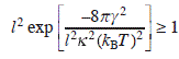
At high temperatures, the density of advacancies increases, resulting in the formation of macro-scale vacancies of monolayer deep. The edge of the macro-vacancy is an additional step. The formation of macro-vacancies is described by nucleation theory. The free energy of a macro-vacancy with radius R is expressed as
where γ is the step stiffness, and δμ is the chemical potential. The first term is the energy increase due to step formation and the second term is the chemical potential decrease due to formation of advacancy cluster. Since the density of macro-vacancy is proportional to the Boltzmann factor, exp[− F(R)/kBT], the clusters larger than the critical value R, which gives maximum of F(R), expand, while those smaller than the critical value shrink. The maximum of F(R) occurs at Rc = γ/δμ,
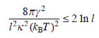
The condition for the formation of at least one macro-vacancy on the terrace within the area of l × l is
On the other hand, from Eq. A1.1,
By comparing these two equations, A1.3 and A1.4, we get
Then, inserting this result into Eq. A1.2, we get
Using typical step spacing l ~103 − 104a,
Since γ is the order of kBT, we obtain the condition for macro-vacancy nucleation,
That is, a macro-vacancy is formed when the terrace size is comparable or larger than the adatom diffusion length.