
Properties of printed films as electrical components and metallization of solar cells
Abstract:
While research is in progress for the development of printed active electronic devices, including printed organic film transistors, power generator devices and memories, our age of information technology is benefitting from integrated circuit (IC) circuits with their integrated active and passive elements in a single chip and from hybrid circuits where active devices are taken from the semiconductor industry to be added to a network of passive electronic components. Thick-film passive components were developed for such hybrid circuits but their application has been spread in other areas and they continue to enter all segments of the electronics industry: military, industrial, data processing, medical, automotive, telecommunications and consumer. This chapter provides an overview of the properties of thick-films applied in this area of electronics, with sections covering resistors, conductors, dielectrics; special emphasis is on the features that make their behavior unique or at least uncommon. Where appropriate, chronological perspective is provided. In addition, the development of thick-film front metallization of silicon solar cells is illustrated.
4.1 Introduction
Thick-film compositions have many properties that render them technologically important, scientifically challenging and facilitate new applications. Some of these properties are unique to thick-film compositions and are not shared by other classes of materials.
The properties of thick-film compositions have been reviewed by many authors in journals and books and have been reported in the patent literature. Some selected reviews are: Altenburg et al. (2002), Borland (2004), Bouchard (1999), Dell’Acqua and Prudenziati (1994), Finch (1969), Kelemen (1970), Kuo (1992), Walton (1975), Larry et al. (1980), Prudenziati (1981), Vest (1991b), Wang et al. (1994), White (2006) and White and Turner (1997).
In this chapter, only some properties of thick-film compositions are reviewed. These properties were selected on the basis of their uniqueness and they are the properties that account for the broadened applications of thick-film compositions. Two unique properties are from the field of thick-film resistors, one is the sheet resistance (ρs) and the second one the temperature coefficient of resistance (TCR). Other selected topics are the Ag-migration of silver-based conductors, Ag front metallization for solar cells and the applications of dielectrics.
4.2 Thick-film resistors
Thick-film resistors (TFRs) have several technologically important properties such as sheet resistance (ρs), temperature coefficient of resistance (TCR), low excess noise, low voltage coefficient of resistance (VCR), stability and trimmability.
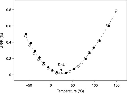
Two of the above-listed properties, ρs and TCR, are unique in the sense that they are not exhibited by other classes of materials widely used in microelectronics and they are still a challenge for theoreticians. ρs has a very broad range, 0.1 to 106 Ω/![]() (see for instance Figure 4.1) and the shape of the Resistance (R) plot as a function of temperature of typical TFR is almost parabolic, as given in Figure 4.2; therefore, the TCR is negative at low temperatures T < Tmin and becomes positive over Tmin where the resistance attains a minimum value.
(see for instance Figure 4.1) and the shape of the Resistance (R) plot as a function of temperature of typical TFR is almost parabolic, as given in Figure 4.2; therefore, the TCR is negative at low temperatures T < Tmin and becomes positive over Tmin where the resistance attains a minimum value.
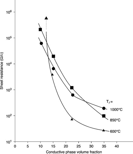
4.1 Sheet resistance as a function of conductor particle volume fraction. Different curves due to samples prepared at different peak temperature T f (after Morten et al., 1994).
4.2.1 Sheet resistance, Rs
The resistance R of a TFR is given by:
where l, w and t are the resistor length, width and thickness, respectively, and ρ is the resistivity in Ω.cm. For a TFR with l = w (one square), the resistance is R = ρ/t; for a TFR with l = w and t = 25 μm the R /25 μm = Rs (Ω/![]() ). Therefore, the resistance of any TF resistor is given by:
). Therefore, the resistance of any TF resistor is given by:
where ![]() is the number of squares or the aspect ratio and t is the dried TFR thickness in microns. Rs defined above is a unit for describing the ‘resistivity’ of TFRs in Ω/
is the number of squares or the aspect ratio and t is the dried TFR thickness in microns. Rs defined above is a unit for describing the ‘resistivity’ of TFRs in Ω/![]() . ρs has very broad range 0.1 to 109 (Ω/
. ρs has very broad range 0.1 to 109 (Ω/![]() ). The low range 0.1 to ~ 10Ω/
). The low range 0.1 to ~ 10Ω/![]() is obtained by the combined use of metallic oxides and precious metals, usually Ag and Pd. The 10–106 Ω/
is obtained by the combined use of metallic oxides and precious metals, usually Ag and Pd. The 10–106 Ω/![]() range is obtained by changing the volume fraction of the metallic oxide in the glass–fillers–conducting materials composite. A typical TF resistor composition consists of glass, fillers and a conducting phase. The TF resistance is a very complex function of many variables, which include the glass, fillers, the conducting phase and TCR modifier concentrations, variables such particle size distribution of all the solid phases, glass composition, processing variable, termination type and composition and substrate type and its composition.
range is obtained by changing the volume fraction of the metallic oxide in the glass–fillers–conducting materials composite. A typical TF resistor composition consists of glass, fillers and a conducting phase. The TF resistance is a very complex function of many variables, which include the glass, fillers, the conducting phase and TCR modifier concentrations, variables such particle size distribution of all the solid phases, glass composition, processing variable, termination type and composition and substrate type and its composition.
Figure 4.1 (Morten et al. 1994) presents ρs as a function of the conducting phase volume fraction. This dependence is also known as ‘blending curve’. Blending curves were the subject of intensive experimental research: effects of glass composition (Vest, 1991a), nature and size of conductive particles (Abe and Taketa, 1989; Listkjewicz and Kusy, 1985; Pike and Seager, 1977; Tamborin et al., 1997), firing conditions (Morten et al., 1994, Vionnet-Menot et al., 2005) and substrate composition (Kurihara et al., 1991) were studied. The shape of these curves, because of their substantial departure from those common to other cermet resistors, were also the subject of a myriad of theoretical speculations (Monneraye, 1978; Pešić, 1988; Pike and Seager, 1977; Prudenziati, 1981; Vest, 1991a).
Nowadays there is a general consensus on a percolative approach in which a relevant role is played by the peculiar distribution of conductive particles embedded in the fired film. This distribution is characterized by large regions of glass that constrain the much smaller conducting grains to be segregated in between the interstices of neighboring glass grains. This ‘segregated microstructure’ forces the classical percolation theories to deviate from the ‘universal’ values of the parameters (see Grimaldi, Chapter 5). As far as the electrical transport is concerned, inter-particle tunneling seems the prevalent mechanism. However, there are still differences in the various proposed models regarding the ‘details’ of the tunneling steps; these are: (1) the assistance of resonant centers, if any, and their possible origin, (2) the contribution of electron hopping on impurity bands or isolated states (also in the interparticle glass), and (3) the presumed contribution of the resistance of the embedded conductive grains (or their clusters) to the whole resistance.
In Chapter 5, Grimaldi explores some approaches to identify the electrical conduction mechanisms in TFRs and offers a view of the current understanding of this subject. Unfortunately, we have to admit that despite the progress in theoretical approaches and enrichment of results, regarding both the microstructure and the electrical behavior, there is little hope of arriving at a quantitative description of the blending curve: ρs is a function of too many variables for a comprehensive treatment with the current knowledge and computer simulations. The development of thick-film resistor pastes is still, and probably will be in the near future, based on empirical methods.
4.2.2 Temperature coefficient of resistance (TCR)
TFRs are known for their low TCR, typically lower than 100 ppm/°C in a temperature range of − 55 to 125 °C. Figure 4.2 presents the typical temperature dependence of resistance R for TFRs. The plot shows a resistance minimum and two branches of R versus T; one ‘semiconducting’ (i.e. R declines when T increases) leading to a negative TCR, and one branch with R behaving as a ‘metal’ thus with a positive TCR. This is a characteristic property of TFRs and, as far as we know, it is a unique one, its appearance near room temperature making TFRs very useful passive components for microelectronic applications and sensors.
A number of models have been proposed over the years to explain both findings: the low TCR values and the minimum of resistance. The issue comes from the consideration that there is no mechanism for combining the high negative TCR (− 7000 ppm/°C) of glasses with positive TCR (e.g. + 7000 ppm/°C of single crystal RuO2, + 3000 ppm/°C of ruthenates), to accomplish TCR values as low as 50–100 ppm/°C. This exercise might be successful for a single relative fraction between the dielectric and conductive component and hence for a single resistivity value. But the mentioned behavior is observed in TFRs on many decades of resistance values; in addition, the cross-over temperature Tmin, from TCR < 0 to TCR > 0 is shifted in the desired direction with small amounts of TCR modifiers. These findings are still sufficient to suggest the essential role of the glass in the TCR control. On the other hand, layers of pure (i.e. without glass) polycrystalline sintered IrO2 and RuO2 prepared (on alumina substrates) by a thick-film technique (Dziedzic and Golonka, 1988) exhibit TCRs which, although lower than that of the single crystal counterparts, are still positive, almost linear and without any minimum in the very broad range of − 200 to 800 °C. Early models for electrical transport in TFRs rested on supposed (and now proved as very unrealistic) microstructures (uniform distribution of constitutive elements, or continuous channels of grains in contact, or homogeneously distributed conductive grains in glassy matrix); the models were criticized by Pike and Seager (1977). Next, the efforts were aimed at identifying a transport mechanism, compatible with the improved knowledge of the microstructure (i.e. the segregated one, mentioned above) capable of introducing a negative TCR. Currently, the most cited models consider tunneling barriers between adjacent conductive grains; the electrical transport through these barriers is thought to be assisted by resonant centers (Pike and Seager, 1977), or by hopping transport, either the nearest neighbor hopping or the variable range hopping (Flachbart et al., 1998; Totokawa et al., 2009), or by intrabarrier metal clusters. Also the models differ about the contribution of the grain resistivity to the total one (e.g. see Pešić, 1988; Pike and Seager, 1977; Prudenziati, 1981; Vest, 1991a).
The TCR > 0 regime has also been explained in terms of the thermal expansion affecting the inter-particle tunneling distances (Kubový, 1995), or by invoking the temperature-induced strain due to the mismatch between the thermal expansion coefficients of the resistor and the substrate (Fawcett and Hill, 2000; Sion et al., 1994).
As the theories on transport mechanisms in insulator–conductor composites are refined these points will be clarified; however, the major step in the knowledge of TFRs will be the progress in description of source, amount, extension and behavior of ‘impurities’ at the interface between the conductive particle and the glass. With this knowledge the development of a new generation of competitive thick-film resistors would be anticipated.
4.2.3 Size effects
Changes of thickness and interactions between the resistive film and its terminations are responsible for the frequently observed influence of the geometry of resistors, mainly their length, on their electrical properties. ‘Size effect’ refers to the change of the effective sheet resistance as a function of the resistor length.
The mean thickness of a set of resistors of various lengths is a function of the resistor length: in a traditional screen-printing process the bowing of the screen can cause the center to be thinner than the edges, and the regions adjacent to the terminations to be thicker. This variation is more influential on short than on long resistors. Consequently, the actual resistance R divided by the aspect ratios of the various resistors in the set does not result in a constant effective sheet resistance Rs, even if the resistivity ρs is a constant. The apparent Rs value is usually lower in short (e.g. 0.2–0.5 mm long) resistors. This situation is largely mitigated with direct-write printing processes (Yang et al., 1999).
Interactions between the resistive film and its terminations are conversely responsible for compositional changes and resistivity variations. The reduction of the effective sheet resistance near the termination is the most frequent case (denoted ‘direct size effect’) but also the reverse effect is possible (inverse size effect). The variety of (sometimes seemingly contradictory) experimental findings reported on the subject is currently consistent with the following picture:
1. Bi diffusion is responsible for a decrease of resistance in RuO2 as well as in ruthenate-based resistors (Prudenziati et al., 1986).
2. Ag diffusion is responsible for a decrease of resistivity in ruthenate-based resistors as well as in RuO2-based systems, provided that the latter are free from aluminium (Prudenziati et al., 1991).
3. Ag diffusion increases the resistance of RuO2-based resistors containing aluminum, already present in the resistor composition or interdiffused from the substrate (Morandi et al., 1991; Prudenziati et al., 1989a).
High resistance in the resistor near the resistor/conductor interface has also been found to arise from changes in the microstructure of the resistor, where RuO2 grains are redistributed and retreated from the region near the conductor interface (Vest, 1991b).
It is interesting to note that the diffusion of Bi partially suppresses the effect of Ag diffusion. Other elements (e.g. Mn) are even more effective in suppressing the inverse effect (Morandi et al., 1991). These are the same elements usually introduced in RuO2-based resistors for the control of the TCR (see Chapter 2). This is the reason why the inverse size effect is rarely observed in films prepared with commercial pastes.
No matter what the origin of the local resistance change, the phenomenon is also associated with changes to other properties such as TCR, long-term stability and current noise. This latter quantity is especially sensitive to conductive-to-resistive layer interactions. Noise spectroscopy is quite effective in discriminating bulk noise from contact noise, if measurements are carried out with samples configured as multiterminal specimens with several side legs equally spaced along the resistor length (Masoero et al., 1990; Mleczko et al., 2008).
4.2.4 Trimming
The commonly observed tolerance of a population of as-fired, screen-printed resistors of the current state-of-the-art quality is between 10 and 20%. At least two factors contribute towards this large deviation from the predetermined resistance value: (1) poor control of macroscopic geometric parameters (such as resistor thickness and lateral edge smoothness, well defined interface resistor/termination) and (2) microscopic uniformity of the active materials, which impacts on the film resistivity. This latter is improved with uniform and very fine conductive particles giving at least half the dispersion of the conventional pastes (Sato et al., 1993), while the former (control of geometry) may be improved through stencil printing instead of screen printing and with optimization of the whole printing process (e.g. mesh orientation of the stencil opening toward the printing direction; Cheng et al., 2007). Printing with dispensing technologies (e.g. MicroPen by OhmCraft, see Chapter 1) can produce very well-defined resistor patterns and thus lower tolerances than conventionally printed resistors (Yang et al., 1999).
Resistors with tolerances within typically 0.5% can be achieved by laser trimming, i.e. by burning away a part of the resistor with a laser beam (commonly a Nd-YAG laser, λ = 1.06 μm) operated in the Q-switched mode in the closed-loop control system, which shuts off the beam when the desired resistor trimming value has been achieved (Fig. 4.3). Laser trimming is applied to resistors designed to have a fired resistance value below the final target value, and may be done on glazed components. The ‘green glasses’ for glazing resistors are in fact optimized for optical absorption of the trimming laser radiation. In hybrid circuits, instead of trimming resistors to specific values, it is customary to trim them to produce a specific output level (e.g. voltage, frequency, current, etc.) from the circuit, a process known as ‘functional trimming’. Laser beams may produce severe thermal shock in the resistors, which leads to microcracks in the neighborhood of the kerf that are a potential source of instability.
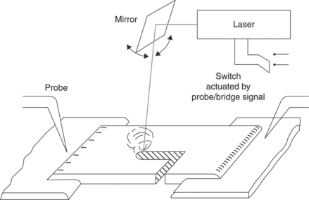
4.3 Laser trimming: a laser beam is moved on the resistor surface to ‘cut’ away a small portion, raising its resistance value. The operation is conducted while the circuit is tested by automatic test equipment.
The need for alternative trimming methods emerged from the development of low-temperature co-fired ceramic (LTCC) circuits and particularly for the adjustment of resistors buried inside laminated tapes, thus not directly accessible by the laser beam. Resistors are susceptible to high voltage pulses and static electricity and so the development of pulse-trimming methods generated renewed interest in these effects, which were originally studied in the 1970s (Seager and Pike, 1976; Stevens et al., 1976). Pulse trimming results in increased resistance in ‘low-decade’ compositions (i.e. TFRs in the range 10–100Ω/![]() ), whereas the opposite effect is observed in high-decade resistors; the origin of these effects has yet to be fully clarified. Pulse height, pulse width, number and repetition rate are parameters of choice to reduce the tolerance at values of 0.5–1%. Reports on the (possible) change of other properties, e.g. current noise, low term stability and TCR values in trimmed resistors, do not agree with each other. For instance, noise level was reported to decrease by Tobita and Takasago (1991), to remain almost unvaried according to Dziedzic et al. (2005) and to increase according to Stevens et al. (1976) and Stanimirovi et al. (2006). Perhaps these discrepancies are due to the different characteristics (compositions, size, terminations) of samples investigated and underline the need for further studies on this subject.
), whereas the opposite effect is observed in high-decade resistors; the origin of these effects has yet to be fully clarified. Pulse height, pulse width, number and repetition rate are parameters of choice to reduce the tolerance at values of 0.5–1%. Reports on the (possible) change of other properties, e.g. current noise, low term stability and TCR values in trimmed resistors, do not agree with each other. For instance, noise level was reported to decrease by Tobita and Takasago (1991), to remain almost unvaried according to Dziedzic et al. (2005) and to increase according to Stevens et al. (1976) and Stanimirovi et al. (2006). Perhaps these discrepancies are due to the different characteristics (compositions, size, terminations) of samples investigated and underline the need for further studies on this subject.
4.2.5 Long time stability – ageing
Resistor changes as a consequence of various storage conditions that simulate processing conditions, such as solder dipping to packaging, or their operating life are common stability criteria. According to the envisaged applications, the resistance drift at temperatures as low as 40 °C with 90% relative humidity, or at exposure to 300 °C for hundreds of hours may be required. A huge amount of data for TFRs aged in various conditions has been collected and cannot be briefly summarized. Here a few significant figures and common trends are reported.
Figure 4.4 shows the results of a study of ageing under an exceptionally wide temperature range (125 to 400 °C): the data suggest that the monotonous resistance drift versus time experienced at the lower temperatures is lost when the ageing temperature ‘approaches’ the softening point of the glassy matrix of the resistors under test (about 630 °C for the case illustrated in Fig. 4.4). Ageing tests at temperatures in the range 150 °C to 300 °C for a given time t, show that: (1) ∆R/R values obey the Arrhenius equation, i.e. ΔR/R(t = const) ~ exp(− E/KT), where K is the Boltzmann constant and E the activation energy (E ~ 0.46 eV in specimens of Fig. 4.4). Also, ∆R/R after isothermal annealing is directly proportional to the square root of time, suggesting diffusion-controlled ageing mechanisms. Similar features have been experienced in other systems (e.g. Coleman, 1979; Rocak et al., 2001; Wheeler, 1985) but are far from exhausting the full picture of ageing phenomena. In fact, at temperatures as low as 60–100 °C, the time dependence of the resistance drift is better approximated by ∆R/R ~ tn with n < < 1/2, e.g.n ~ 1/3 to 1/7 was reported by Coleman (1979) and Wheeler (1985).
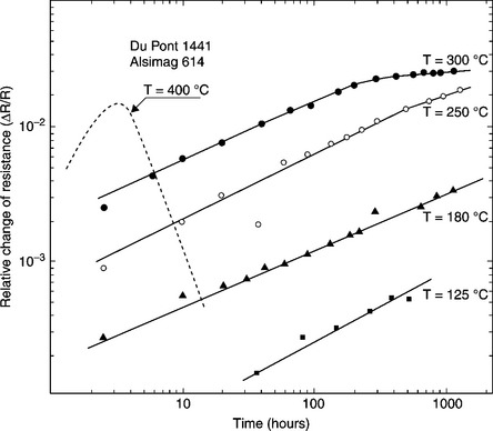
4.4 Relative change of resistance of DuPont 1441 resistor after exposure at different temperatures and times in lab air (after Prudenziati and Morten, 1983).
Two distinct contributing factors have been identified, i.e. (1) the resistivity change of the bulk resistor material with time and (2) the influence of the conductor materials, mainly Ag-based, particularly for the small resistor geometry. Experiments have shown that the drift of resistivity is affected by:
• Composition and microstructure, for instance the size of the conductive phase in the paste that is otherwise identical in composition and processing (Dietrich et al., 2009), or amount of the conductive phase in otherwise identical pastes and processing conditions (Prudenziati et al., 1981/82).
• The environment, e.g. rich or poor of oxygen, humidity (Coleman, 1979; Sinnadurai and Wilson, 1982). Out-diffusion and in-diffusion of oxygen have been postulated to interpret the effect of the atmosphere and the reduced shift of encapsulated (glazed) resistors compared to unprotected ones.
• Stress and strain, as shown by Dell’Acqua et al. (1982): the drift of resistors stored at 125 °C in stressed conditions (both tensile or compressive) is higher than that of the unstressed ones, a result that should be further systematically investigated to look for possible correlations with the composition, strain sensitivity and ageing conditions.
• Composition of conductive terminations: it has been found that in some resistors printed with Ag conductors, the relative change of resistance follows a linear time-dependence, suggesting a rate limited reaction, and gives negative resistance drift. Moreover, this contribution to the whole drift is higher for shorter resistors than in longer ones (Rocak et al., 2001). The total drift for high annealing temperatures and short resistors may be negative.
• Substrate composition (Jakubowska and Pitt, 1995; Morten and Prudenziati, 1983; Wheeler, 1985).
• The type of laser or pulse-trimming, and the relative parameters.
The total resistance drift is dependent on the sum of all the mechanisms. There is normally a dominant mechanism over a given temperature range for a given resistor system and set of processing conditions, which enables the characteristic parameters to be identified. A comprehensive picture of all these mechanisms has never been reported, but it may be envisaged that it should include phenomena such as strain relaxation and interactions between the film constituents, with the substrate and with the environment
4.3 Conductors
4.3.1 Introduction to conductors
Applications of printed conductive films, especially thick-film conductors, are referred to in many chapters of this book. Printed conductors are in fact useful or even essential to realize inductors, heaters, resistive temperature detectors (RTDs), heat dispersing layers in high power circuits, to accomplish electrodes for display, electromagnetic/radiofrequency shields, electrodes for capacitors and sensing elements, as internal electrodes in multilayer ceramic capacitors (MLCC) and multilayer varistors (MLVs), metallization for photovoltaic devices and fuel cells (SOFCs), sacrificial layers for MEMS. In hybrid circuits, thick-film conductors serve three primary tasks: (1) to terminate thick-film resistors and capacitors, (2) to interconnect discrete devices mounted on the substrate with the thick-film passives or other discrete devices, placed on the same surface or, through vias, on different levels in multilayer circuits, (3) to fulfill the needs for the circuit package, e.g. heat sink, solder pads, sealing lids. This myriad of applications calls for different compositions and processing conditions.
Table 4.1 presents a list of selected (intrinsic) properties of metals used in thick-film compositions.
Table 4.1
Some properties of precious and base metals used in thick-film conductor compositions
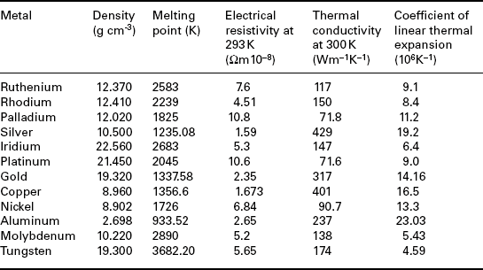
Source: Emsley (1991).
The resistivity ρ (Ωcm) of the pure element, reported in the table results in the sheet resistance Rs given by ρ/25 10− 4; hence, for example, ρ = 10 μΩ cm corresponds to Rs = 4 mΩ/![]() . The fired thick-film conductors exhibit resistivity that is higher by a factor of 3 to 15 than that of the parent metal, because of the inevitable porosity in the film and the presence of binder phases (oxides, glass; see Chapter 2) added in the paste to improve the adhesion to the substrate, as sintering aids, etc. Also, in most thick-film conductors the functional phase is not a pure element but a binary or ternary alloy combination, which leads to lower electrical conductivity but circumvents or mitigates some side problems (leaching in solders, migration, etc.).
. The fired thick-film conductors exhibit resistivity that is higher by a factor of 3 to 15 than that of the parent metal, because of the inevitable porosity in the film and the presence of binder phases (oxides, glass; see Chapter 2) added in the paste to improve the adhesion to the substrate, as sintering aids, etc. Also, in most thick-film conductors the functional phase is not a pure element but a binary or ternary alloy combination, which leads to lower electrical conductivity but circumvents or mitigates some side problems (leaching in solders, migration, etc.).
In selecting a composition, considerations are due primarily to the electrical resistivity and adhesion to the substrate, but, depending on the applications, also to good line definition, wire bondability or leach resistance, compatibility with other components and substrate, migration resistance, porosity (permeability to gases) and cost. Efforts in research and development over many decades have enabled the introduction of pastes and processes to meet all these requirements adequately.
Despite their higher price, noble metals and alloys (especially Ag, Pd, Pt, Au and their binary or ternary alloys) are mostly used in conductive formulations, because they can be processed in air and offer higher corrosion resistance, wider compatibility and better electrical properties than non noble-based thick-film conductors.
For specialized applications, base metals such as Al, Ni, Cu, Mo and W are used. For example, Ni is the choice for the internal electrodes of current MLCC and magneto-resistive sensors, whereas W and Mo are used in high-temperature co-fired ceramic (HTCC) technology, Al is the major ingredient for back-contact metallization of Si solar cells and for heat dispersing layers in high power packages, etc. (Wang et al., 1994).
Because of such various formulations and properties, it would be impossible to address all the thick-film conductors in full. Therefore we will confine ourselves to some considerations on silver-based conductors, i.e. on the most important class of thick-film conductors. This class includes films based on Ag and its alloys with Pd, Pt and Au. The alloys enhance the solder leach resistance (Pt) and/or increase silver migration resistance (Pd).
Also, these systems offer substantial cost benefits over the precious metals, which are more expensive and very fluctuating in price as a function of market. Although in recent years (since 2004) the cost of Ag has increased sharply following the increase in the cost of Au, Pt and Pd, it (Ag) is still below $50/troyoz, therefore at least an order of magnitude lower than the cost of Au, Pd and Pt.
Because of its unique and unsubstitutable properties, Ag is the major player in thick-film conductors and expected to maintain its position in the near future. An increase of Ag use in thick-film conductors is expected in view of the projected (BCC reports, 2010) increase in the volume of energy-related devices such as silicon photovoltaic cells. In view of this central role projected for silver, in this section only properties of silver conductor compositions are reviewed. One subject is the electrolytic migration of silver-based conductor compositions and the second subject is Ag front metallization for silicon solar cells.
4.3.2 Silver migration
Silver (Ag)-based conductors on dielectrics or between dielectrics (crossovers) in humid atmosphere and under d.c. field, migrate as ions (Ag+) from one site (the anode) and deposit on another site (the cathode) as dendrites. The dendrites may grow on a surface or through the dielectrics and electrically connect two conductors’ tracks, thus leading to shorts. This phenomenon is known silver (electrolytic) migration and is a major drawback of Ag conductors. Factors affecting the ion migration encompass paste composition, high d.c. electric field caused by the voltage drop across closely spaced conductors, ambient temperature and relative humidity, encapsulation and finally composition, roughness and contamination of the substrate (Coleman and Winster, 1981; Lin and Chan 1996, 1997; Naguib and MacLaurin, 1979; Wang et al., 1994). To compare the relative role of these factors and to evaluate different materials, information is quickly collected with the so-called water-drop (WD) tests in which a drop of deionized water is placed to bridge the gap (typically 250–1000 μm wide) between two conductor tracks, and the migration of Ag is observed upon applying a bias (a few volts) between the two tracks. The temperature humidity bias (THB) tests are more adequate to evaluate the migration resistance under (quasi) real operating conditions. In these tests, samples are studied under controlled temperature and relative humidity (RH) conditions (e.g. 85–90 °C, 85–90% RH), then somewhat more severe conditions than those projected for most circuits, which otherwize would force experiments in a time domain of days or even years. In THB, the decline in insulation resistance or the increase of leakage current across the closely spaced conductors under d.c. bias are measured as a function of time, or until the time to failure.
During WD tests, Ag migration rate under d.c. field of 0.1 V/mil (40 V/cm) with electrodes containing pure silver, either on bare alumina substrate or dielectric layers, is so fast as to cause shorts within 60–90 s. The migration is reduced by 100 times in Pd/Ag conductors with a Pd content higher than 10% (Naguib and MacLaurin, 1979). In THB tests under equivalent electrical conditions, the Ag migration rate is approximately 104 times lower than in WD tests. However, the glass component in the conductor paste and the method of preparing the ink may have a significant influence on its migration susceptibility, regardless of its Pd content. An additional method to minimize the migration is to encapsulate the fired film with an organic coating or a glaze layer (like DuPont 9137 used by Naguib and MacLaurin (1979), now replaced DuPont QQ550), which prevents the moisture condensation or ionic contamination on the surface.
It has been shown that migration of the Ag on the surface of – as opposed to through the thickness of – dielectric crossover was the main failure mode in these structures. Silver migration in thick-film conductors on substrates of different compositions and cleanness preparation, as well as in chip attachment resins, was reported by Coleman and Winster (1981). They stressed the importance of producing and maintaining the substrate surface free from debris and contamination. Only under very controlled conditions is the rate of Ag-migration related to the Ag content of the film. Glass as an encapsulation and as a barrier between conductors is effective in retarding migration and, to great extent, resin encapsulants have a similar effect.
The anodic formation of PdO was suggested as the effect limiting Ag dissolution and the occurrence of Ag migration with PdAg conductors, by increasing the amount of Pd from 5 to 20%, until the complete disappearance of migration at 30% Pd (Lin and Chan, 1996). In a second study, Lin and Chan (1997) have shown that conductors made from mixed Ag and Pd powders are more migration-resistant than those prepared from alloyed AgPd powders, having the same Ag/Pd ratio. Liu et al. (2011) reported on the advantages, in terms of resistance to electro-migration, offered by composite powders, such as Ag-plated Cu powders substituting silver powder in the films.
One of the challenges for the near future is to lower the cost of Ag-based conductors and maintain their properties. One obvious way is to use Ag-coated Cu powder in polymer thick-film conductors for relatively low processing and operating temperatures. For ceramic-type conductors to be processed at 850 °C, using Cu-coated Ag, new innovative approaches are required to stabilize the copper in its metallic (alloyed) state.
4.3.3 Thick-film metallization for solar cells
Several printing techniques have been used to deposit front Ag metallization on silicon solar cells. Screen printing is the leading technique nowadays. However, ink-jet printing has been modified, special compositions have been developed and sophisticated machines have also been developed to make it a strong second runner for printing front Ag metallization on silicon solar cells.
The metallization compositions for screen and ink-jet printing contain very similar materials: silver metal as a major component, glass powder(s), additions such as metal oxides or mixed oxides and an organic vehicle. The solid ingredients for ink-jet printing are typically nanometer size and for screen-printing paste they are larger and range from one submicron to several microns. The glass frits used are lead borosilicates, bismuth–lead borosilicates and lead-free glasses, which are based on bismuth–zinc borosilicates. Many publications and patents have addressed the subjects of processing, compositions and the mechanisms of forming ohmic contact between the silver and the silicon. In a recent publication, Schubert et al. (2006) reviewed the existing models and recent developments. Schubert et al. (2002) also suggested a redox reaction between silicon and metal oxides in the glass and proposed the following reaction:
to describe the interaction of glass frit with silicon.
Sopori et al. (2007) reviewed the fundamental mechanisms in the fire-through contact metallization of solar cells.
A more detailed understanding of front metallization contact with silicon and current transport mechanisms were the result of the recent studies. However, many issues still remained to be unraveled.
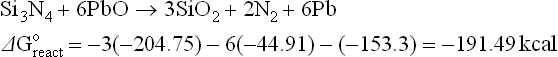
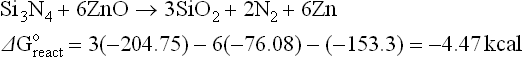
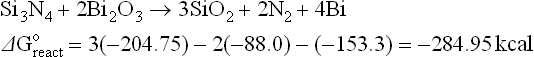
The thermodynamics of possible reactions among paste or ink ingredients (Ag, glass, oxides additives), silicon and anti-reflective coating, SiNX are outlined below to aid the understanding of the interactions. A simple approach is to consider the standard free energies (taken from Handbook of Chemistry and Physics: Weast, 1987–1988) of key ingredients as separate entities and use these energies to estimate the possible direction of specified reactions. The assumptions used in these calculations are that the reactions occur between crystalline ingredients at room temperature (298 K). In reality, the reactions are between crystalline and vitreous ingredients at temperatures higher than 298 K. The differences between estimated and real values of free energies of reactions (ΔGreacto) may be large. However, for large absolute values (reactions 4.1 to 4.8, excluding 4.4), they show a clear trend.
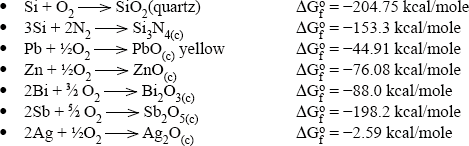
Some possible reactions among the paste ingredients, antireflection coating and silicon base are:
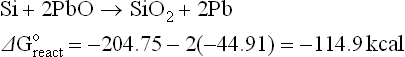
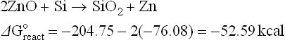
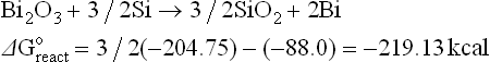
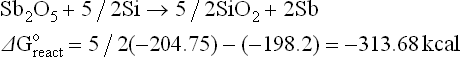
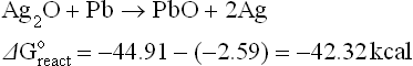
The estimated free energies of reactions 4.1, 4.3, 4.5 and 4.6 indicate that it is very likely that glass ingredients such as PbO, Bi2O3, ZnO and Sb2O5 (a similar conclusion is expected for Sb2O3) will be reduced by the silicon base. The zinc oxide is a special case: although the estimated free energies of reactions may be small negative numbers, the reaction can be driven to the right by the high vapour pressure of the liquid zinc, owing to its low melting point and fairly low boiling point. Thus, zinc oxide as a glass ingredient or as an additive is expected to be reduced by the silicon base and interact via redox reaction with the antireflection coating.
All the metals that are expected to be formed by the redox reactions (Pb, Bi, Zn, Sb) will interact with the silver oxide in the glass (see, for example, reaction 4.7) and oxidize with the formation of metallic silver.
The literature describes the interactions of the Ag front metallization with the antireflection coating (Si3N4) as fired through, dissolution or etching. The reactions above (4.2, 4.4 and 4.8) point out that the mechanism might be a redox reaction to form silicon dioxide, which will dissolve in a glass, nitrogen gas and metal (Pb, Zn, Bi).
Besides the interactions with the silicon base and dissolution of metallic silver, the glass forms a layer on the silicon solar cell. Dissolution of silver in glasses used for the preparation of silver front metallization was reported by Prudenziati et al. (1989a).
Layers of glass on silicon solar cells were reported by Ballif et al. (2003; 1989b), Nakajima et al. (1983); Prudenziati et al. (1986b); Schubert et al. (2006); Thuillier et al. (2000), and in citations quoted in Schubert et al. (2006).
Since the glass wets the silver and forms a layer on the silicon, the electrons have to tunnel through the glass from the silicon (Nakajima et al., 1983; Prudenziati et al., 1996). The glass is a dielectric material and even with a dissolution of 1–3 wt% of Ag during the short thermal processing cycle, it can be argued (Sopori et al., 2007) that its conductivity is not high enough to support transport. Moreover, most of the silver in the glass is ionic and the volume fraction of metallic silver is too low to make the glass sufficiently conducting. These arguments of the low solubility and low volume fraction of Ag have to be contrasted with the vitreous enamel resistance material developed by Janakirama-Rao and Murphy (1964). These authors have shown (see Chapter 2 for a detailed discussion) that by the introduction of ionic silver into the glass, the conductivity of the conductor was increased by several orders of magnitude compared to a conductor that contains the same glass but without ionic silver.
Improvement of the photovoltaic performance of silicon-based solar cells can be accomplished by increasing the light absorption area. Special Ag front metallization compositions need to be developed that will allow the deposition of very fine conductor lines. The new compositions will probably be based on very fine solid ingredients, such as nanoparticles of silver and dielectric materials, and organic ingredients, which will allow deposition of fine conductor lines by conventional thick-film techniques and other methods such as ink-jet printing. Other important future issues are to decrease the cost of materials and processing.
4.4 Dielectrics
4.4.1 Applications
Thick-film dielectrics find applications in a variety of different areas. They encompass the traditional dielectrics for hybrid microelectronics to the more recent areas of sensors, actuators, MEMS, optoelectronic devices (displays), heaters and energy converters (e.g. fuel cells). Thus a wide range of thick-film inks is available today. Specific properties for some of the applications will be delineated in the following sections, with reference to the related literature.
The general basic requirements for thick-film dielectrics are the same for any dielectric materials, such as appropriate dielectric strength, dielectric constant and loss, mechanical strength and environmental stability. However, additional features are associated with the printed film structure and processing; these are compatibility with other system elements, the sequence of depositions and firing operations.
The traditional thick-film dielectrics fall into three different classes: (1) crossover and multilayers, (2) overglaze and sealants, (3) capacitors. The specific functions and properties of these films have been reviewed by Bouchard, 1999; Dell’Acqua, 1994; Hoffman, 1984; Larry et al., 1980; Vest 1991b.
Crossovers allow conductor lines to be printed over one another, through multiple firing steps, without ‘flowing’ in the refiring process. Crystallizable glasses, e.g. calcium zinc aluminosilicates, which precipitate celsian (BaAl2Si2O8) or hardystonite on firing, are adequate composition for crossover. In multilayer circuits, a dielectric is printed over the entire first layer of printed and fired components, which are electrically connected through holes or vias in the dielectric. In this case, the composition may be similar to crossovers, but requirements to be met are more stringent to match the thermal expansion coefficient, reach high dielectric strength and inhibit ionic migration. Typical properties are: relative permittivity in the range 8–14, breakdown voltage 500–1000 V/25 μm; insulation resistance R > 1010 Ω · cm at 100 Volts DC.
Overglaze dielectrics provide passivation to underlying resistor and capacitor films. They are usually glasses that flow and coalesce at low temperature (e.g. 400 to 500 °C) to minimally change the properties of the underlying films.
Capacitor dielectrics need to exhibit as high a dielectric constant as possible. The past two decades have brought outstanding progress in the development of high-performing capacitors, by means of relaxor ceramics. These are ferroelectric perovskites typified by lead magnesium niobate (PbMn1/3Nb2/3O3) with a ferroelectric transition at a temperature (the Curie temperature Tc or Curie point) near room temperature (Lejeune and Boilot, 1985). All the ferroelectric materials exhibit a maximum (peak) permittivity, often as high as 15 000–30 000, near Tc. Relaxors are characterized by their notable diffuse (50–100 °C around Tc) transition; moreover, Tc can be shifted to the optimum value for the envisaged operations by means of known changes of composition (e.g. solid solutions of different perovskites) and processes (including powder size, thermal processes). Relaxors, with their complex physical and technological properties, are a very rich chapter of electronic ceramics (Swartz, 1990). Their applications in thick-films give us compounds with dielectric constants up to 10 000–15 000, and other excellent dielectric properties for films fireable in air with noble metal electrodes at ‘standard’ firing temperatures (850–950 °C). Hence, integral thick-film capacitors may be accomplished with capacitance density of up to 3000 pF/mm2. For high integration and high volumetric efficiency (e.g. in cellular phones, computers), single-layer thick-film capacitors have been supplanted by MLCCs, i.e. structures in which many dielectric layers and internal electrodes are alternately stacked and the internal electrodes are connected in parallel. In the current technology, the number of layers is typically 500–700, and the areas are smaller than 1 mm2. With this structure, noble metals for the internal electrodes are too expensive, and therefore are replaced by Ni. This latter has to be fired in reducing ambient because of its tendency to severely oxidize in air; this requirement in turn calls for a ‘non-reducible’ dielectric, in place of lead-based relaxors. Today the materials of choice for imbedded dielectrics in LTCC are variously doped BaTiO3. A perovskite oxide, (k ~ 15.000), in which the dopants substitute for the A ion (Ba) or for the B ion (Ti) with proper charge, balance and stabilize the ideal perovskite structure ABO3. They have to inhibit the decline of insulation resistance otherwise due to oxygen vacancies in the BaTiO3 lattice. The development of this technology, which required a deep understanding of electronic defect phenomena in complex materials, today provides millions of units of MLCCs at prices of around 0.01 $/unit. The capacitance may be 1 to 100 μF in case sizes as small as 1.0 × 0.5 mm2 (Kishi et al., 2003).
While the majority of thick-film dielectrics are tailored to meet requirements for hybrid circuits, components and systems on alumina and LTCC, a variety of compositions for other applications and substrates have been developed, for example:
• Dielectric for multilayers and sealants designed to match the thermal expansion coefficient of AlN (e.g. Ferro Corporation, multilayer dielectric 10-054).
• High-temperature compositions for use in planar oxygen sensors (e.g. ESL 4492).
• Porous overcoat for planar oxygen sensors (e.g. ESL 4550).
• Pb- and Cd-free thick-film glass designed for sealing low thermal expansion substrates, such as silicon and soda lime, at reduced firing temperatures. For hermetic sealing of wafer-level, MEMS packaging and other micro-mechanical devices, such as vibration, SAW, accelerometer sensors and gyroscopes (Ferro Corporation).
• Glasses for the hermetic sealing on alumina, ceramic packages, glass optoelectronic displays and other applications calling for low glazing temperatures (T ~ 400 °C) (e.g. Ferro Corporation, 1161 HZ).
• Dielectrics-on-steel (e.g. DuPont QM42, ESL D4914, Heraeus IP-222-SL for sensors and heaters, Heraeus IP-211 for Cr-steel).
• Insulation of aluminium, for integral packaging of devices, such as high-emitting LEDs (e.g. ESL 4003 and 4604-A).
In each new product, challenges were addressed to meet one, or a variety of, specific requirements: tightness or porosity of the film, long-term stability at high operating temperatures, unusual low (or high) processing temperature or adhesion with the envisaged substrate.
4.5 References
Abe, O., Taketa, Y. Mathematical relation between RuO2 volume fraction and resistance of thick-film resistors. J Phys D: Appl Phys. 1989; 22(11):1777–1781.
Altenburg, H., Plewa, J., Plesch, G., Shpotyuk, O. Thick-films of ceramic, superconducting, and electro-ceramic materials. Pure Appl Chem. 2002; 74(11):2083–2096.
Ballif, C., Huljie, D.M., Willeke, G., Hessler-Wyser, A. Silver thick-film contacts on highly doped n-type silicon emitters: structural and electronic properties of the interface. Appl Phys Lett. 2003; 82(12):1878–1880.
BCC reports. Thick-film devices, processes and applications, 2010. [Report Code: AVM046B].
Borland, W., Ceramic thick-films process and materialsBuchanan R.C., ed. Ceramic Materials for Electronics. 3rd ed. 2004:527–580.
Bouchard, R.J., Thick-film technology: an historical perspective. Ceramic Transactions 100 (Dielectric Ceramic Materials). 1999:429–442.
Cheng, P.L., Leung, S.Y.Y., Law, T.W., Liu, C.K., Chong, J.I.T., et al. Quantitative analysis of resistance tolerance of polymer thick-film printed resistors. IEEE Trans Comp Packag Technol. 2007; 30(2):269–274.
Coleman, M.V. The effect of nitrogen and nitrogen–hydrogen atmospheres on the stability of thick-film resistors. Proceedings of the International Microelectronics Symposium. 1979:255–262.
Coleman, M.V., Winster, A.E. Silver migration in thick-film conductors and chip attachment resins. Microelectronics Journal. 1981; 12(4):23–29.
Dell’Acqua, R. Thick-film dielectric materials. In: Prudenziati M., ed. Thick-film Sensors. Amsterdam: Elsevier; 1994:99–111.
Dell’Acqua, R., Prudenziati, M. Thick-film resistors. In: Prudenziati M., ed. Thick-film Sensors. Amsterdam: Elsevier; 1994:85–97.
Dell’Acqua, R., Dell’Orto, G., Simonetta, A., Canali, C. Long term stability of thick-film resistors under strain. Int J Hybrid Microel. 1982; 5:82–84.
Dietrich, S., Kretzschmar, C., Partsch, U., Rebenklau, L. Reliability and effective signal-to-noise ratio of RuO2-based thick-film strain gauges: the effect of conductive and glass particle size. 32nd International Spring Seminar on Electronics Technology. 2009:1–6. [ISSE 2009].
Dziedzic, A., Golonka, L. Electrical properties of conductive materials used in thick-film resistors. J Mater Sci. 1988; 23(9):3151–3155.
Dziedzic, A., Kolek, A., Ehrhardt, W., Thust, H. Advanced electrical and stability characterization of un-trimmed and variously trimmed thick-film and LTCC resistors. Microelectronics Reliability. 2006; 46(2–4):352–355.
Emsley, J. The Elements, 2nd ed. Oxford: Clarendon Press; 1991.
Fawcett, N., Hill, M. A contribution to the debate on the resistance–temperature characteristics of thick-film resistor materials. Sensors and Actuators A. 2000; 86(1–2):52–57.
Finch, R.G. Thick-film materials. Thin Solid Films. 1969; 3(3):189–199.
Flachbart, K., Pavlìk, V., Tomašovičová, N., Adkins, C.J., Somora, M., et al. Conduction mechanism in RuO2-based thick-films. Phys Stat Sol (b). 1998; 205(1):399–404.
Hoffman, L.C. An overview of thick-film hybrid materials. Ceram Bull. 1984; 63(4):572–576.
Jakubowska, M., Pitt, K. Influence of the contacts and firing process on the properties of thick-film resistors on alumina and dielectrics. J Mater Sci: Mater Electron. 1995; 6(2):75–78.
Janakirama-Rao, B.V., Murphy, R.M. Resistance material and resistor made therefrom. 1964. [US Patent 3 154 503, October 27].
Kelemen, D.G. Metallographic aspects of thick-film technology. Metallurgical Transactions. 1970; 1:667–677.
Kishi, H., Mizuno, Y., Chazono, H. Base-metal electrode-multilayer ceramic capacitors: past, present and future perspectives. Jpn J Appl Phys. 2003; 42(1):1–15.
Kubový, A. Model of electric conductivity of thick-film resistors Part III. Temperature dependence of sheet resistivity. Ceramics-Silikáty. 1995; 39(1):30–33.
Kuo, C.C.Y. Thick-film circuit materials. Gongneng Cailiao. 1992; 23(5):265–269.
Kurihara, Y., Takahashi, S., Yamada, K., Endoh, T., Kanai, K. Thick-film resistors for AlN ceramics. IEEE Trans on Compon, Hybrids and Manufact Technol. 1991; 14(1):199–203.
Lejeune, M., Boilot, J.P. Low firing dielectrics based on lead magnesium niobate. Mater Res Bull. 1985; 20(5):493–499.
Larry, J.R., Rosenberg, R.M., Uhler, R.O. Thick-film technology: an introduction to the materials. IEEE Trans on Compon, Hybrids and Manufact Technol. 1980; CHMT-3(2):211–225.
Lin, J.C., Chan, J.Y. On the resistance of silver migration in Ag-Pd conductive thick-films under humid environment and applied d.c. field. Mater Chem Phys. 1996; 43(3):256–265.
Lin, J.C., Chan, J.Y. Resistance to silver electrolytic migration for thick-film conductors prepared from mixed and alloy powders of Ag-15Pd and Ag-30Pd. J Electrochem Soc. 1997; 144(5):1652–1659.
Listkjewicz, E., Kusy, A. Computer simulation of thick resistive films as two component percolation systems; segregation of the conducting component. Thin Solid Films. 1985; 130(1–2):1–15.
Liu, Y., Long, J., Zhu, X., Liu, W., Electrochemical migration characteristics of Ag-plated Cu powders in conductive thick-film. Adv Mater Res. 2011:146–147. [1070–1074].
Masoero, A., Morten, B., Prudenziati, M., Stepanescu, A., An improved technique of measuring the contact noise in thick-film resistorsAmbrozy A., ed. Noise in Physical Systems. Proceedings 10th International Conference. Akademia Kiado Budapest, 1990.:561–564.
Mleczko, K., Zawiślak, Z., Stadler, A.W., Kolek, A., Dziedzic, A., et al. Evaluation of conductive-to-resistive layers interaction in thick-film resistors. Microelectron Reliab. 2008; 48(6):881–885.
Monneraye, M. Les encres sérigraphiables en microélectronique hybride: les matériaux et leur comportement. Acta Electron. 1978; 21(4):263–281.
Morandi, M., Morten, B., Prudenziati, M., Argentino, E., Ruffi, M.G. Manganese in ruthenium-based thick-film resistors. Materials Engineering. 1991; 2(3):421–433.
Morten, B., Prudenziati, M. Thermal aging of thick-film resistors. Hybrid Circuits. 1983; 3:24–26.
Morten, B., Sirotti, F., Prudenziati, M., Manfredini, T. Evolution of ruthenate-based thick-film cermet resistors. J Phys D: Appl Phys. 1994; 27(10):2227–2235.
Naguib, H.M., MacLaurin, B.K. Silver migration and reliability of Pd/Ag conductors in thick-film dielectric crossover structures. IEEE Trans Comp, Hybrids, Manufact Technol. 1979; CHMT-2(2):196–207.
Nakajima, T., Kawakami, A., Tada, A. Ohmic contact of conductive silver paste to silicon solar cells. Intl J Hybrid Microelectron. 1983; 6(1):580–586.
Pešić, L. A review of thick-film glaze resistors. Microelectr J. 1988; 19(4):71–87.
Pike, G.E., Seager, C.H. Electrical properties and conduction mechanisms of Ru-based thick-film (cermet) resistors. J Appl Phys. 1977; 48(12):5152–5169.
Prudenziati, M. Conduction mechanisms in thick-film resistors. Procedings of 3rd European Hybrid Microelectron Conference Avignon. 1981:1–10.
Prudenziati, M., Morten, B. Thermal aging and stability of thick-film resistors. Int J Hybrid Microelectron. 1983; 6(1):96–100.
Prudenziati, M., Morten, B., Ruffi, G., Argentino, E., Iachetti, C. Size effect due to silver diffusion in RuO2-based resistors. 7th European Hybrid Microelectron Conference. 1989. [Hamburg, May].
Prudenziati, M., Moro, L., Morten, B., Sirotti, F., Sardi, L. Ag-based thick-film front metallization of silicon solar cells. Active and Passive Electr Components. 1989; 13(3):133–150.
Prudenziati, M., Morten, B., Olumekor, L., Moro, L., Tombesi, A. Interactions between terminations and thick-film (cermet) resistors: the role of bismuth. J Phys D: Appl Phys. 1986; 19(2):275–282.
Prudenziati, M., Morten, B., Taroni, A. Characterization of thick-film resistor strain gauges on enamel steel. Sens Actuators. 1981/82; 2(1):17–27.
Prudenziati, M., Sirotti, F., Sacchi, M., Morten, B., Tombesi, A., et al. Size effects in Ru-based thick-film resistors: RuO2 vs. pyrochlore-based resistors. Active and Passive Electro Components. 1991; 14(3):163–173.
Rocak, D., Belavic, D., Hrovat, M., Sikula, J., Koktavy, P., et al. Low-frequency noise of thick-film resistors as quality and reliability indicator. Microelectron Reliab. 2001; 41(4):531–542.
Sato, K., Watanabe, M., Seino, T. Development of thick-film thermal print head for full color video printer. Int J Microcircuits Electron Pack. 1993; 16(2):145–160.
Schubert, G., Fischer, B., Fath, P. Formation and nature of Ag thick-film front contacts on crystalline silicon solar cells. Proceedings of Photovoltaics in Europe Conference. 2002:343–346. [Rome].
Schubert, G., Huster, F., Fath, P. Physical understanding of printed thick-film front contacts of crysalline Si solar cells – review of existing models and recent developments. Solar Energy Materials and Solar Cells. 2006; 90:3399–3406.
Seager, C.H., Pike, G.E., Electrical field induced changes in thick-film resistors. Proc Int Microelectronics Symp ISHM-USA. 1976:115–122.
Sinnadurai, N., Wilson, K.J. The aging behavior of commercial thick-film resistors. IEEE Trans Comp, Hybrids Manufact Technol. 1982; CHMT-5(3):308–317.
Sion, R.P., Atkinson, J.K., Turner, J.D., A novel model for the temperature characteristic of a thick-film piezoresistive sensor. Sens Actuators A. 1994:41–42. [460–464].
Sopori, B., Mehta, V., Rupnowski, P., Appel, J., Romero, M., et al, Fundamental mechanisms in the fire-through contact metallization of Si solar cells: a review. presented at 17th Workshop on Crystalline Silicon Solar Cells and Modules: Materials and Processes. 2007. [August 5–8, Vail Cascade Resort, Vail, Colorado USA].
Stanimirovi, I., Jevti, M.M., Stanimirovi, Z. Performances of conventional thick-film resistors after multiple high-voltage pulse stressing. Proceedings of 25th International Conference On Microelectronics (MIEL 2006). 2006. [Belgrade, Serbia and Montenegro, May 14–17].
Stevens, E., Gilbert, D., Ringo, J. High-voltage damage and low-frequency noise in thick-film resistors. IEEE Trans Part, Hybrids, Pack. 1976; 12(4):351–356.
Swartz, S.L. Topics in Electronic Ceramics. IEEE Trans Electr Insul. 1990; 25(5):935–987.
Tamborin, M., Piccinini, S., Prudenziati, M., Morten, B. Piezoresistive properties of RuO2-based thick-film resistors: the effect of RuO2 grain size. Sens Actuators A. 1997; 58(2):159–164.
Thuillier, B., Berger, S., Boyeaux, J.P., Luagier, A. Observation of mechanisms of screen-printed contact formation during heat treatment of multicrystalline silicon solar cells by transmission electron microscopy. Proceedings of 28th IEEE PVSC. 2000:411–413. [Ancorage].
Tobita, T., Takasago, H. New trimming technology of a thick-film resistor by the pulse voltage method. IEEE Trans Comp, Hybrid Manufact Technol. 1991; 14(3):613–617.
Totokawa, M., Yamashita, S., Morikawa, K., Mitsuoka, Y., Tani, T., et al. Microanalyses on the RuO2 particle–glass matrix interface in thick-film resistors with piezoresistive effects. Intl J Appl Ceram Technol. 2009; 6(2):195–204.
Vest, R.W. A model for sheet resistivity of RuO2 thick-film resistors. IEEE Trans Comp, Hybrids, Manufact Technol. 1991; 14(2):396–406.
Vest, R.W. Materials aspects of thick-film technology. In: Buchanan C., ed. Ceramic Materials for Electronics. 2nd ed. Marcel Dekker Inc; 1991:435–488.
Vionnet-Menot, S., Grimaldi, C., Maeder, T., Ryser, P., Strässler, S. Study of electrical properties of piezoresistive pastes and determination of the electrical transport. J Eur Ceram Soc. 2005; 25(12):2129–2132.
Walton, B. Principles of thick-film materials formulation. Radio Electron Eng. 1975; 45(3):139–143.
Wang, S.F., Dougherty, J.P., Huebner, W., Pepin, J.G. Silver-palladium thick-film conductors. J Am Ceram Soc. 1994; 77(12):3051–3072.
Weast R.C., ed. Handbook of Chemistry and Physics, 68th ed., Boca Raton, Florida: CRC Press Inc, 1987/88.
Wheeler, J.M. Thick-film conductors and resistors on dielectrics for high reliability applications. Hybrid Circ. 1985; 8:24–27.
White, N. Thick-films. In: Springer Handbook of Electronic and Photonic Materials. New York: Springer; 2006:717–731.
White, N.M., Turner, J.D. Thick-film sensors: past, present and future. Meas Sci Technol. 1997; 8(1):1–20.
Yang, P., Dimos, D., Rodriguez, M.A., Huang, R.F., Dai, S., et al, Direct-write precision resistor for ceramic packages. Mater Res Soc Symp Proc 542 (Solid Freeform and Additive Fabrication). 1999:159–164.