
Multilayer low-temperature co-fired ceramic systems incorporating a thick-film printing process
Abstract:
Since the first application of low-temperature co-fired ceramics (LTCC) – a radar chip manufactured by DuPont and Hughes – in the 1980s, LTCC has gone through many changes, evolving from a simple multilayer substrate technology to a complex microelectronic system suitable for ‘intelligent’ packages with buried passive components, heat sinks, sensors, actuators, energy harvesters and even microsystems. Moreover, novel materials and enhanced processes have been introduced constantly. This chapter presents LTCC technology, starting from material development followed by processing steps and proposed applications. Future trends and challenges are discussed, and literature containing more detailed descriptions is listed.
6.1 Introduction
The introduction in 1947 of a tape casting-method for ceramic materials by Glenn Howatt (Howatt et al., 1947) opened up the possibility of fabricating multilayer ceramic devices with embedded electrodes. High-temperature co-fired ceramic (HTCC) technology, in particular, was utilised in the very beginning to fabricate multilayer ceramic capacitors. Components were made of common ceramic compositions like Al2O3 or BaTiO3, and since they required a moderately high sintering temperature (well over 1100 °C), refractory metals like tungsten were used for electrodes. Although nowadays HTCC technology is also utilised in broader application areas like radio frequency devices (RF) or microelectromechanical systems (MEMS), novel substrates capable of handling large numbers of signal lines or substrates enabling higher-conductivity electrodes were needed in modern electronics. This was achieved with low-temperature co-fired ceramics (LTCCs), in which the ceramic materials employ a lower sintering temperature (< 1000 °C) and embedded electrodes are made of silver or copper.
LTCC technology is based on the simple idea of printing conductive patterns using pastes on tape-cast unsintered (‘green’) ceramic sheets, which are then stacked and joined together in a lamination process, forming a solid bulk body after sintering at about 850 °C. A huge amount of LTCC products have been introduced, especially for automotive, military, space and telecommunication purposes. Table 6.1 shows some commercially available LTCC materials and their most important properties. These systems have a fully conductive paste series for embedded and post-fired electrodes, and many vendors provide dielectric and resistive pastes as well.
Table 6.1
Some commercially available LTCC materials and their properties
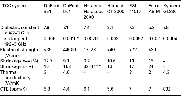
*At 10 GHz.
**Depends on tape thickness.
The largest suppliers of LTCC systems that include LTCC tapes and pastes are Du Pont, Heraeus, ESL and Ferro. However, many companies manufacture LTCC only for their own purposes. The popularity of LTCC technology, resulting from its superb electrical and mechanical properties together with its relatively low cost, can be easily seen in Fig. 6.1, which shows the number of publications dealing with this topic.
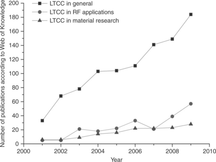
6.1 LTCC publications introduced since 2001, based on Web of Knowledge (http://wok.mimas.ac.uk).
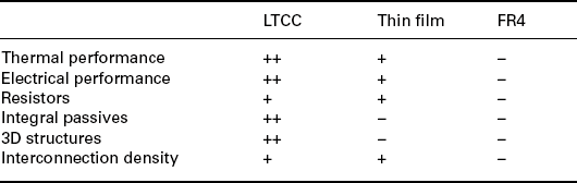
Properties like excellent mechanical and electrical stability even in harsh environments and at high temperatures, good dielectric properties at high frequencies, together with a coefficient of thermal expansion (CTE) matching that of silicon and resistance to different chemicals, make LTCC technology very competitive in comparison with, for example, printed circuit boards (PCBs) made of polymer materials (Table 6.2). LTCC technology is also used to fabricate hermetic packages. Additionally, the fact that the structures are co-fired makes parallel processing possible, which greatly reduces manufacturing times. Also, computer aided design (CAD) and short process times make LTCC a perfect technology for rapid prototyping, ensuring fast turnarounds in production and short time-to-market.
6.2 Low-temperature co-fired ceramics (LTCC) compositions
The main objective of LTCC research has been to enable the manufacture of multilayer ceramic structures with highly conductive embedded electrodes, thereby challenging polymer-based structures. For dielectric compositions the objective has been (1) to make electrical circuits for hazardous environments (automotive industry) and (2) to form modules with extremely low losses (telecommunication industry), both providing improved thermomechanical and electrical performance. However, in order to fabricate multifunctional ceramic multilayer modules, not available with polymer materials, non-linear LTCCs also need to be developed. This chapter discusses the approaches used to reach these goals.
6.2.1 Dielectric LTCCs
LTCC compositions widely used today in industrial products are mostly dielectric. LTCCs commercially available in tape form and have a relative permittivity value ranging from 4 up to 20, with a very competitive dielectric loss even at GHz frequencies, thus being compatible with silver/copper paste systems used to form embedded electrodes (Sebastion and Jantunen, 2008). In practice, these materials are developed either by adding low softening point glass to crystalline dielectric powder, or by utilising a fully glass system as a starting material. In the first approach, a high sintering temperature dielectric crystalline powder, like Al2O3, TiO2 or SiO2, is used as a starting material to which low softening point glass is added to form a matrix that enables the use of a lower sintering temperature (Knickerbocker et al., 1993; Imanaka, 2005). The sintering process can be non-reactive or reactive, depending on whether the glass material serves only as a bonding agent or reacts with the dielectric filler. These compositions are also commonly made of several different phases, especially when advanced glasses are developed to manage properties such as glass fluidity, crystallisation, softening point or foaming. Several commercial dielectric LTCCs follow this route, for example DuPont 951, which is composed of Al2O3, CaZrO3 and glass (Steinberg et al., 1998).
In the second approach, the starting material is mainly in the glassy phase, which devitrifies during the sintering process, forming as fully crystalline structure as possible, with high density, to achieve the desired electrical properties. To enhance the crystallisation it is also common to add some nucleating agents. Commercial LTCC from Ferro A6-M follows this procedure, using CaO-SiO2-B2O3 glass as a starting material, devitrifying it to wollastonite crystal surrounded by a small amount of borosilicate glass.
However, in both of these approaches the main objective is to achieve a dense structure with a low amount of glassy phases, which commonly reduce the thermomechanical and electrical properties of the final composition. This is the main reason several versatile methods for developing LTCC compositions have also been introduced. It is possible to use a mixture of the approaches mentioned above: decrease particle size (Marques et al., 2006), utilise materials with a low sintering temperature (Udovic et al., 2004) or use a chemical process where the ceramic dissolves in flux forming crystalline oxides (Jean and Lin, 2000). Two-step processes have also been found to be an effective method for decreasing the amount of glassy phases and thus keeping the original electrical properties as far as possible. Hsi et al. (2008) reported that a BaTiO3-based LTCC composition sintered at 850 °C had high relative permittivity (1700), being close to the high sintering temperature composition value (Hsi et al., 2008). This was performed with a two-stage process using calcium boron silicate glass with a LiF coating (Fig. 6.2).
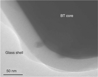
6.2 Transmission electron microscopy (TEM) bright field image of Barium Titanate (BT) particle coated with calcium boron silicate glass with LiF (Hsi et al., 2008).
One very effective approach to developing LTCCs that enable advanced electrical properties is to use sintering aids. This approach has been widely used for high-permittivity dielectrics reaching values of relative dielectric constant close to 500 at GHz frequencies (Kim et al., 2002). Commonly used sintering aids are oxides like B2O3, LiF, CuO, V2O5 or Bi2O3, and the amount added is in the region of a few wt% (Kim et al., 1999; Lee et al., 2003; Yokoi et al., 2005; Zhang et al., 2006). The main reason for the success of this approach is that a minimum amount of glassy phases or even glass-free microstructures can be achieved, thus enabling the preservation of the original dielectric properties of the starting material. Additionally, it is clear that if different LTCC materials could be developed with this approach, this would allow the use of similar sintering mechanisms for all compositions enabling their co-firing in multifunctional applications.
Although the first challenge in the development of LTCC compositions is to decrease the sintering temperature close to 900 °C, the work itself is far more complicated when commercial products for industrial purposes are targeted. Devitrification, sintering and liquification mechanisms and rates, viscous flow mechanisms, wetting, chemical reactions, phase formation, glass fabrication routes, etc. should be well managed during the sintering process. Slurry compositions that enable tape casting also create their own requirements, since they contain organic additives that should be burned out before densification so that a minimum amount of carbon remains in the microstructure (Tummala, 1991). In addition, to achieve the desired electrical performance, sintering behaviour, thermomechanical properties, chemical compatibility together with production and material cost as well as repeatability should be taken into account. Furthermore, multilayer LTCC structures fabricated with embedded electrodes also require that the LTCC composition be compatible with the conductive paste; this issue should be analysed at a very early stage. This is a major challenge, because LTCC compositions are commonly complicated, and in fact all commercially available systems include pastes meant just for these compositions, enabling embedded, post-fired or bonding electrodes.
A very comprehensive review of developed dielectric LTCC compositions and process requirements is presented by Sebastian and Jantunen (2008) and Imanaka (2005).
6.2.2 Non-linear LTCCs
If all the benefits available within LTCC technology are to be utilised, process-compatible non-linear ceramics should also be developed in addition to dielectric ones. Electroceramics including compositions from the highly insulating end of electrical performance up to superconductors should be considered. Especially interesting are sensors, actuators and energy-harvesting applications made of piezoelectrics, frequency-tuning elements made of ferroelectrics, non-linear resistors for varistor applications, and magnetic/ferrite compositions. So far, the main interest has been in magnetic/ferrite compositions made primarily from NiZn, NiCuZn, MnZn, CoZn and LiZn compounds, Ba- or Sr-based hexagonal ferrites or YIG garnets using sintering aids like V2O5 or Bi2O3 and Ag2O, or a small addition of glass like Bi2O3-B2O3-SiO2-ZnO (Yan et al., 2006; Matz et al., 2009). Especially interesting compositions have been reported by Ganne et al. (2007) and Lisjak and Drofenik (2007), based on Y3-2x/3CuxFe5O12 and Ba3Co1.4Cu0.6Fe24O41, respectively. Suitability for GHz frequency applications is one of the main challenges with these materials. A good example of the power of this kind of research is the solenoid transformer introduced by Shamim et al. (2007), or ferrites integrated in high-frequency antenna structures that provide self-biased structures, enabling miniaturisation of the devices to a great extent (Sun et al., 2007).
BaSrTiO3 in the ferroelectric or paraelectric state is also a very interesting material. In the ferroelectric state, this material is used for memory devices. In the paraelectric state, no domains exist and lower losses are achieved, which is why these compositions are used to tune the frequency or phase of telecommunication devices. All related LTCC compositions are based on BaSrTiO3, having different portions of Ba/Sr to adjust the Curie temperature. Several glass compositions like the ones based on SiO2, Al2O3, B2O3 and BaO have been studied to decrease the sintering temperature, but the most successful compositions are made using sintering aids. In 2004, Valant and Suvorov, and Jantunen et al. introduced compositions that utilise a very small addition of LiF and B2O3 + Li2O, respectively (Valant and Suvorov, 2004; Jantunen et al., 2004). Since then, LTCC modules made of these materials have been reported (Deleniv et al., 2005). One interesting study mentioned earlier is a BaTiO3-based LTCC-compatible composition (Fig. 6.2). Tunability ((C(0) – C(E))/C(0)) (where C(0) is the capacitance with 0 V applied field, and C(E) is capacitance with applied field equal to E) achieved with E = 4 V/μm was 50%, being very close to the values achieved with a pure composition fabricated with thin-film processes (Hsi et al., 2008).
In recent years, development related to piezoelectric ceramics has been concentrated on the important topic of lead-free compositions. These compositions are commonly based on K0.5Na0.5NbO3, first introduced by Jaeger (Jaeger and Egerton, 1962) and Haertling (Haertling, 1967). Since then, these materials have been developed to enable more controlled and lower-temperature sintering by modifying their main composition, using sintering aids like MnO2 or Bi2O3 (Nagata, 2008; Takao et al., 2006) and utilising advanced processing methods like spark plasma sintering (Li et al., 2006). Although this field of science is still waiting for major progress before true LTCC integrations are performed, LTCC-compatible piezoelectric compositions are able to provide a very wide range of applications like frequency-tunable elements for telecommunication purposes, already proposed by Joshi et al., (Joshi et al., 2007) and piezoelectric films on LTCC (Hrovat et al., 2006).
Additional application examples that could be useful if embedded in LTCC structures are varistors. These components are commonly based on ZnO, SiO2, TiO2 or SnO2, with different performance-modifying additives (MnO2, Sb2O3 with a two-step process, semiconductive glass) used to lower the sintering temperature (Zhao et al., 2007; Nehm, 2008; Honkamo et al., 2007). In addition to simple high-voltage protection devices in low-voltage automotive and semiconductor electronic devices, applications could include, for example, a circuit comprised of an antenna input, a signal input and output and a switching unit, wherein the antenna input is connected to a device that protects against electrostatic discharges (Block et al., 2008).
These kinds of multi-material integrations enable the creation of applications not available in any way other than by utilising advanced LTCC compositions.
6.2.3 Pastes for LTCC systems
All LTCC tape manufacturers provide a wide selection of system-compatible Ag, Ag-Pt, Ag-Pd, Pt and Au thick-film pastes for embedded electrodes, conductive vias and post-fired surface electrodes enabling also soldering or bonding. However, efficient packaging through the multilayer structure is only achieved if capacitors, resistors and non-linear structures like sensors or heaters can be also seamlessly integrated. Since the commercial LTCC tapes have commonly low relative permittivity (< 10) and the tape thickness is relatively high (> 50 um), other methods to embed large capacitors are needed. For embedded structures, high permittivity pastes have been introduced. ESL, for example, provides pastes with dielectric constant between 50 and 250, fulfilling the Electronic Industries Alliance X7R standards (± 15% Δc over –55 ºC ~ + 125 ºC) (Feingold et al., 2003). Also, other structures are proposed to be fabricated with LTCC-compatible pastes. The challenge with embedded resistors in LTCC is the high resistance tolerance, normally 20–30%, and several groups have investigated this problem through modelling, resistor materials’ development and careful processing control (Hsi et al., 2003; Horvth, 2008; Birol et al., 2005, 2006). Wang et al. (2002), for example, have estimated that to reach the 10% resistance tolerance goal, the print thickness of the resistor tolerance must be no more than 8%. However, there is still much work to be done to enable accurate and reliable embedded resistors in LTCC modules.
In addition to embedded passive elements, varistors, temperature sensors, heaters and frequency-tuning elements utilizing thick-film pastes have also been proposed. One example is a Zn-based varistor using thick-film LTCC pastes suitable for electronic circuits protecting semiconductive devices, for example, for high voltages (Mis et al., 2009). The structures, co-fired at 850 or 950 °C, showed nonlinearity coefficient α up to 23 with capacitor-like varistors having Pt terminations. Additionally e.g. temperature sensors (Vanek et al., 2009), heaters (Kim et al., 2010), pressure sensors (Hrovat et al., 2008) and antenna tuning (Tick et al., 2008) embedded to LTCC modules using compatible thick-film pastes have been reported.
Although over 200 articles related to thick-film materials and structures for LTCC systems have been reported, e.g. including, most recently, on multisensors for compressed air diagnostics (Fournier et al., 2010), ultra low gas concentration sensors (Karioja et al., 2010) and piezoelectric cantilevers for energy harvesting (Kok et al., 2009), pastes are one interesting option for advanced research in LTCC modules.
6.3 LTCC manufacturing methods
6.3.1 Design of LTCC products
Before introducing the LTCC fabrication process, an overall design guideline for LTCC products is given. The first challenge is to manage tape shrinkage. In general, this means that if a new tape is taken into production, shrinkage in all directions (x, y and z) should be measured using structures closely mimicking the modules to be fabricated. Many tape systems have almost the same shrinkage in all directions (5–20%), but so-called zero shrinkage systems can also be selected where horizontal (x–y) dimensional change is only 0.20% ± 0.04% (see Table 6.1). However, it is important to remember that the next fabrication steps, like lamination, can affect shrinkage. The general structural design rules that enable production of quality LTCC products with commonly available processes are presented in Table 6.3 and Fig. 6.3. The dimensions given are suggestive, and are based on feasible dimensions with safety margins. As with other thick-film methods, careful design is a prerequisite for a functioning LTCC product. The main limitations are caused by the thick-film printing process and the method of fabricating vias. The limitations of the latter also depend on the thickness of the tape itself. The shrinkage behaviour of the ceramic tapes is also a challenge: it depends especially on the selected LTCC system, as shown in Table 6.1.
Table 6.3
General dimension guidelines for an LTCC product
| Key | Meaning | Minimum dimension (μm)* |
| A | Distance between soldering base and module edge (see also key M) | 125 |
| B | Distance between conductor and via | 175 |
| C | Distance between an SMD (surface-mount device) and conductor | 200 |
| D | Conductor width | 150 |
| E | Distance between two conductors | 150 |
| F | Distance between conductor and module edge | 300 |
| G | Distance between conductors in a meshed ground plane | 550 |
| H | Distance between ground plane and via | 300 |
| I | Meshed ground plane conductor width | 250 |
| J | Via diameter | 200 |
| K | Smallest distance between adjacent vias in same tape layers | 2.5 × ø(via) |
| L | Minimum distance between staggered vias in successive tape layers | 2 × ø(via) |
| M | Minimum distance of a via to the edge of the module | 3 × ø(via) |
Key parameters from A to M are illustrated in Fig. 6.3.
*These are suggestive dimensions based on current proofed technology.
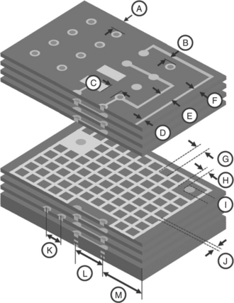
Additionally, large conductive planes, like ground planes, should be implemented as a meshed structure. To reduce the possibility of delaminating tape layers and to reduce bending of the ceramic during sintering, the area of the conductive surface should be less than 50% of the total surface area of the layer. The main reason for this is the differences in the shrinkage behaviour of ceramic tape and thick-film printed paste. Additionally, sintering of symmetrical structures to form flat, dense structures should be selected, if possible. However, several manufacturers use device-oriented tape designs and tape thicknesses, two-step lamination processes, etc., thus enabling clearly smaller dimensions than presented here. The state-of-the-art in LTCC process capabilities is presented in the design guidelines of each LTCC tape manufacturer and in related publications (see the reference list at the end of the chapter).
6.3.2 General LTCC manufacturing methods
The general LTCC fabrication process is presented in Fig. 6.4, which introduces the process from mixing of the raw materials to final inspections of the LTCC products.
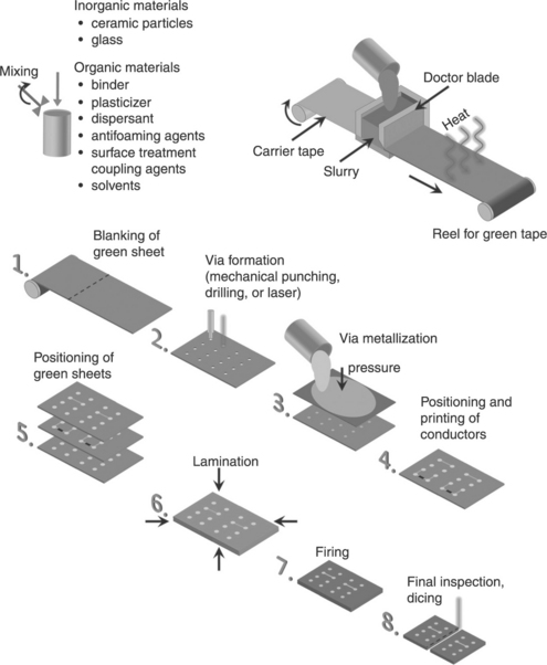
One can select ready-cast tapes on reels or sheets from a manufacturer and compatible conductive paste or start from fabrication of the ceramic material itself. However, if commercial tapes are used, understanding the method of producing the green tapes enables better management of the whole process. The tape fabrication method explained briefly here is described in detail, e.g. by Mistler and Twiname (2000).
After choosing the LTCC composition, as explained in Chapter 2, the slurry from which the green tape is cast is prepared. This includes mixing of the LTCC composition with solvents and organic additives. This is commonly performed in several steps, starting with addition of solvents and dispersants, followed by mixing binders, plasticiser, etc. All the additives have their own special role in enhancing the mixing or casting processes or tape properties, as listed below (Imanaka, 2005):
• binder helps to keep the green tape together during processing;
• plasticiser increases flexibility and thus helps to make the material easier to shape;
• deflocculant/dispersant ensures that the particles do not become agglomerated (i.e. it prevents the formation of flocks) and that they are dispersed uniformly in the cast tape (i.e. to result in a homogenous suspension);
• antifoaming agents help during the tape casting process to ensure that the slurry does not foam, which would result in voids within the produced tape;
The tapes are then fabricated by doctor blade or knife casting in the desired thickness using a carrier tape, usually made of cellulose acetate, Teflon®, Mylar® or cellophane (Gongora-Rubio et al., 2001). Drying the tapes in ambient conditions or by heating results in solid, flexible tapes that can be stored on reels and cut into sheets. The thickness of commercially available tapes generally ranges from 50 to 500 μm, while available widths are roughly from 20 to 30 cm (8 to 12 inches).
Blanking the green sheet (step 1 in Fig. 6.4) to the desired shape can be done, e.g. with a professional paper cutter or a laser. The tape casting direction (i.e. the direction in which the tape carrier was moved during casting) must be known and marked on the tape (this direction is always marked on commercially sold sheets). The reason for this is that the tape shrinks differently in different horizontal directions. To balance shrinkage, each consecutive tape layer should be rotated 90 ° when stacking the green sheets. After blanking, the tape is heated in an oven, typically at 120 °C, for five minutes to release mechanical stresses (induced in the tape cutting) that affect shrinkage of the green tape.
Vias (step 2 in Fig. 6.4) are used to link two layers of conductors vertically through ceramic material or to form channels or cavities. So far, the minimum diameters of vias in LTCC technology are in the range of 30–50 μm with a mechanical punching machine (Hagen and Rebenklau, 2006), and in the same range using laser micromachining (Wang et al., 2006). These two methods are the main via formation methods, but other methods are also available, such as milling, which currently yields dimensions larger than 100 μm. In the past, electron beam machining has also been proposed. (Yau et al., 1991, 1993)
Currently, some of the main challenges in via formation by punching are burr formation, edge breakout during punching, and carrier tape intrusion into the tape (Rhim et al., 2006; Imanaka, 2005). A combination of tape properties (tape thickness, material composition, i.e. its mechanical properties) and process properties (punching speed, tool clearance) mainly affect these. Because the green tape also includes hard ceramic particles, abrasion of the punching tool needs to be taken into account (Imanaka, 2005).
Via formation by laser processing enables formation of high aspect ratio (i.e. thickness/diameter) vias. Also, as no mechanical damage is inflicted on the surrounding green tape, a shorter pitch between vias can be used than with a mechanical puncher (Yau et al., 1993). However, problems with lasering include tapering of the vias and softening or melting of the glass phase, which may fill up the via hole.
With laser processing, the amount of glass in the green tape affects its processability; namely, the more glass there is compared with the ceramic phase, the more likely it will soften or melt during processing and fill the via partly or fully (Kita et al., 2002). The wavelength of the laser and the absorption wavelength of the green tape often differ, but in an ideal case all the energy of the laser is absorbed by the green tape, resulting in fast sublimation of the material. If the structure is to include cavities or channels, they are also formed in this phase. Finally, alignment holes for further processing steps are made in the tape, enabling accurate printing of conductors and stacking of green sheets in the later phases.
Via metallization (step 3 in Fig. 6.4) is a critical process during LTCC manufacturing. Besides electrical/thermal conductor material, the vias may be filled with dielectric, resistive or functional material (see section 6.3.3). Vias are filled using a screen-printing machine or a via filler machine. With a via filler machine, pressure is applied on top of a stencil that has filled via paste, forcing it to flow through stencil openings located in the corresponding places to via holes in the green tape. To avoid contamination of the areas near the vias, paste filling should be done through the carrier tape side. Another way to fill vias is with a screen-printing machine. The green tape is placed on a flat surface (a porous plate) and suction is applied to keep the tape in place whilst printing the paste. The paste printing process, which is applicable also in via filling, is presented in the next section. However, by using a via filler machine it is possible to use higher pressure in the filling process, which allows filling large aspect ratio vias. In addition to via paste, powder can also be used in the filling process, but this includes a risk of voids due to the lower fluidity of powder compared with a material in paste form (Imanaka, 2005).
The success of the filling depends on process variables like pressure and time, material variables like viscosity of the paste, chemistry, and geometrical variables including the shape of the via or its aspect ratio. At the same time, the process is very delicate; adjusting some parameter may result in underfilling or overfilling of the vias, damage to the tape, etc. If the vias are filled with the supporting carrier tape, as is usually the case, there will often be extra via paste left when removing the carrier tape before possible printing of catch pads and lamination. Added to this, the shrinkage of via metallization materials is typically much less than that of the LTCC. This results in a bumpy profile in the fired structure (Sunppan et al., 2006), bringing challenges to the component attachment phase, for example. Structural design modifications (e.g. staggered vias) and material selection are needed to avoid this effect.
Metallization of microvias (< 100 μm in diameter) is especially sensitive to different parameters; the most likely problem is that the aspect ratio is too high, which results in underfilled vias. On the other hand, vias that are too large cause problems afterwards because the via material might not stay in place during handling of the tape.
After filling of the vias, a screen-printing machine is used to print the conductors, resistors, dielectrics, etc. on the tape (step 4 in Fig. 6.4). The screen-printing method commonly used in LTCC manufacturing, also known as gap printing, is an off-contact method, where the screen makes contact with the green tape only at the point where the squeegee pushes the paste through the mesh openings (see Fig. 6.5).
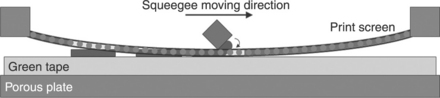
A print screen with a pattern is used to print the paste on top of the green sheet. The screen is commonly made of metal or nylon wires meshed together. The screen includes a photoreactive emulsion which is exposed to UV light with an exposure mask that includes the desired pattern. Typically, the emulsion thicknesses used are around 10–30 μm. In LTCC screen printing, the mesh count usually varies from 200 to 400 holes per square inch, with a higher mesh count able to produce finer detail, but also increasing the possibility of clogging. Both the emulsion thickness and the mesh size needed depend on the paste properties (viscosity, particle size, etc.). The printing paste is a non-Newtonian, more specifically, thixotropic substance, meaning that its viscosity drops as the shear rate increases. Another important property of the paste is its recovery time, which indicates how quickly the viscosity of the paste is restored (Imanaka, 2005).
Four main factors affecting the quality of printing are:
• paste properties (viscosity, particle size);
• screen properties (mesh, emulsion thickness/opening size);
• tape properties (material, surface roughness: the carrier tape side is smoother);
• printing parameters (squeegee speed and pressure, printing gap size, etc.).
Both sides of the green tape can be printed; i.e. after printing the top side, the tape is dried in an oven (typically at 120 °C for 5 minutes), the carrier tape is removed and printing is done on the underside. Minimum conductor width in a typical process is 150 μm, but by using specialised techniques such as direct gravure printing or photoimageable inks (e.g. Du Pont’s Fodel®), for example, conductors less than 50 microns in diameter can be created (Kittilä et al., 2004; Wang et al., 2000). The conductor layer print screen also has openings for the via catch pads that are used to ensure an electrical connection between vias and printed pattern. A rough rule of thumb is that the size of the catch pad should be about 50–100 microns larger in diameter than that of the via if the via is to be smaller than 200 microns in diameter, although recently there have been examples of microvias without catch pads (Wang et al., 2006).
With screen printing, basic elements such as resistors can be integrated in the product. It must be noted, however, that the absolute value of the resistor may deviate from the designed value by tens of percents, especially when making resistors embedded in the structure due to shrinkage, burn-out leftovers and so on.
After the printing phase, the carrier tapes are removed and the green sheets are stacked together using a mechanical or optical aligner (step 5 in Fig. 6.4). In a mechanical alignment system, the green tape, which includes holes for this purpose, is aligned with the substrate, which again has pins in the corresponding positions. In an optical aligning system, the alignment is done with the aid of a camera. Although mechanical aligning is generally used, the optical system is more accurate. As mentioned above, stacking should be done so that the consecutive tape layers are rotated (90 °) in order to minimise the difference in shrinkage in the x and y directions.
To improve the adhesion of the tape layers and thus facilitate handling of the tape at this phase, some drops of ethanol may be spread on the edges of each tape layer, e.g. with a needle. After stacking, the pack is dried in an oven (90 °C for 30 minutes) to evaporate the ethanol. Another way to ensure that tapes stay aligned during handling before lamination is to use hot iron for punctual joining on the edges of the structure. This step can be automated by using so-called stack and tack machines.
In the lamination phase (step 6 in Fig. 6.4), the tape layers are attached together by thermocompression, i.e. by applying heat and pressure to the green tape stack. It was reported in 2001 by Gongora-Rubio et al. (2001) that the highest number of laminated layers can be close to 80. However, four years later, Peterson et al. (2005) showed structures with up to 300 layers.
Uniaxial lamination is perhaps the most commonly used method where, after attaching a stress release foil to both sides of the LTCC stack and installing a silicon mat to equalise pressure everywhere, the stack is placed between two heating plates that compress the tape in the z direction. Typically, the lamination is done at a temperature of around 70–80 °C and a pressure of 20–30 MPa (200–300 bar, i.e. 2900–4350 psi) for 10–20 minutes, depending on the tape used. Isostatic lamination is used to enhance the adherence of the green tapes and the shrinkage behaviour. It is very important for the lamination phase to be successful, since it affects final properties, sintering shrinkages and the probability of later delaminations.
If cavities are used in the stack, some form of support is generally needed during lamination to reduce bending of the stack, rounding of the corners, etc. In the case where the cavities are located on the substrate, rubber inserts can normally be used. However, if the cavities are inside the LTCC module, fugitive or sacrificial materials are needed. (Khoong et al., 2010)
Sintering, i.e. firing (step 7 in Fig. 6.4) is the phase where the laminated green tape package is taken to such a high temperature that neighbouring particles are bonded together by atomic diffusion. This results finally in a monolithic structure. Firing is usually done in a box oven because the temperature can be controlled more accurately, but belt ovens are also used in mass production.
The laminated package is placed on a flat surface, such as a thick Al2O3 plate. A typical LTCC sintering profile is depicted in Fig. 6.6. First, the temperature is raised to 400–450 °C at a rate of a few degrees per minute, after which the organics are burned out. Then the temperature is swiftly raised to 850–875 °C, which is kept for 10–20 minutes. Finally, the temperature is allowed to settle down to room temperature. The whole sintering phase takes about eight hours. During sintering, densification of the basic LTCC composition takes place, resulting in typical green tape shrinkage of 5–20% compared with the sintered product.
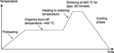
Depending on the LTCC system and the materials used, sintering is done in either an oxidizing or a reducing atmosphere. Especially if copper conductors are used, a reducing or neutral atmosphere is preferred in order to achieve adequate conductivity (Gongora-Rubio et al., 2001; Imanaka, 2005).
After the co-firing phase, some post-processing, like printing of post-fire conductors, may be performed on the fired package. The post-firing profile may differ from the co-firing profile, depending on the material used, but it never exceeds the highest temperature used in the co-firing process.
Next, the monolithic LTCC package is inspected (step 8 in Fig. 6.4) with an optical, acoustic or X-ray microscope, followed by functionality testing with electrical probing, for example. Finally, the structure is diced using a diamond saw or a laser.
6.3.3 Advanced methods for manufacturing and future trends
LTCC process technology has developed tremendously since it was first introduced. Experiments are showing, for example, that piezoelectric cantilevers (Heionen et al., 2007) and optical fibres (Sobocinski et al., 2008) can be integrated into the LTCC even before co-firing. Also thermal management will become more and more important in the future due to increasing packing density. Thermal loads can be dealt with, for instance, using thermal vias (Zampino et al., 2002) or liquid cooling (Barlow et al., 2009). This has already resulted and will surely further result in modifications of the common LTCC process. The possibilities of LTCC technology have been enhanced by ingenious inventions in the following areas:
• Fabrication of complex 3D microstructures by lasering and mechanical (hot) embossing tools (e.g. cavities and microchannels on the scale of a few dozen microns, for micro-opto-electromechanical systems (MOEMS), microfluidistics, waveguides, etc.) (Andrijasevic et al. 2007; Maw et al. 2007; Rabe et al. 2007).
• Shape-preserving buried cavities are created during sintering, e.g. by printing conductors on the opposite sides of the green tape (Espinoza-Vallejos et al., 1998).
• Process modification to create cavities without the need for (carbon-based) sacrificial volume material (SVM) (Barlow et al., 2009).
• Other lamination techniques to create 3D structures (sacrificial material (does not decompose or decomposes partly during sintering), fugitive material (decomposes fully during sintering), etc.)
• Photolithography of LTCC conductors (e.g. Du Pont’s Fodel® paste) with the use of a laser to create fine lines down to 10 μm in width. (Corbett et al., 2005)
• Patterning of LTCC by etching partially sintered tapes, (Park et al., 1998; Espinoza-Vellejos and Santiago-Aviles, 2000; Gongora-Rubio et al., 2001).
• Via fabrication by acetone jet. With this method, Park et al., 1998, for example, have manufactured microvias of 25 microns in diameter (Park et al., 1998; Gongora-Rubio et al., 2001).
• Room temperature lamination with the aid of an adhesive tape (Piwonski and Roosen, 1999; Roosen, 2001), by gluing, (Gurauskis et al., 2005), or otherwise chemically (Jurkow et al., 2009).
• Embedding optical fibres in LTCC (Golonka et al., 2005; Sobocinski et al., 2008).
• Technological development to achieve zero shrinkage horizontally (pressure-assisted sintering, use of sacrificial tapes, zero-shrinking tape) in order to fabricate products with great uniformity (Mikeska et al., 1992; Rabe et al., 2005).
• Embedded functional materials used in applications such as varactors (Tick et al., 2008).
6.4 An overview of LTCC applications
6.4.1 LTCC in packaging and microelectronics
When LTCC was introduced to the market, no one expected the variety of applications within which it is used today. Evolution of the technology allowed it to broaden its margins from simple multilayer substrates to complex ‘intelligent’ packages, sensors, microsystems and more. Each new feature presented to the technology – co-fired resistor pastes, co-strained tapes or co-fireable functional materials – opened new possibilities, but also issued new challenges. Nowadays, LTCC technology is commonly used in RF technologies, wireless communication and packaging. New applications include sensors, actuators and microsystems together with microfluidic lab-on-chips. High yield, fast prototyping and turnaround, flexibility of design, high reliability and relatively low cost have made LTCC the cornerstone of modern electronics.
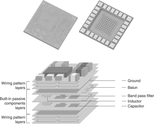
The first LTCC applications, a radar chip for the F-22 jet fighter and a multilayer substrate for IBM and Fujitsu mainframe computers, were presented in the 1980s (Imanaka, 2005; Golonka, 2001). At that time, LTCC was used mainly as a multilayer PCB. The ability to implement signal lines on different levels within the substrate allowed reaching packaging levels unavailable to standard PCBs. Multilayer composition made it possible to separate ground planes from signal lines, wirings from passives, receivers from transmitters and so on, for ease of designing, inspection and better properties. Furthermore, LTCC’s superb microwave properties, such as low-loss and low-resistivity conductors, made it a perfect solution for RF devices (Golonka, 2001; Jantunen et al., 2003). Microwave strip lines, switches, antennas and baluns can be easily manufactured, either as discrete elements of very small size or embedded between thin sheets of LTCC. The possibility of integrating passive elements within the substrate, together with bare dice mounting, allows manufacturing of complete high-frequency devices with excellent properties at relatively low cost.
Applications in the area of RF modules vary from singe/dual/triple-band Global System for Mobile Communications (GSM) transceivers and Global Positioning System (GPS) devices to Bluetooth, Wi-Fi wireless communications and others (Lim et al., 2002; Lin et al., 2004; Ohata et al., 2003). Figure 6.7 presents a RF module and its schematic cross-section, manufactured by Kyocera. Embedding passive functions inside the module allowed a 30% reduction in size compared with the previous built-up substrate approach (Kyocera, 2007).
A common element in smartphones and notebooks – the Bluetooth module – is presented in Fig. 6.8, in this case manufactured by IMST. This second-generation Bluetooth module has an integrated, inverted-F antenna structure, which has proved to have better performance than surface-mount device (SMD) solutions (Kulke et al., 2003).
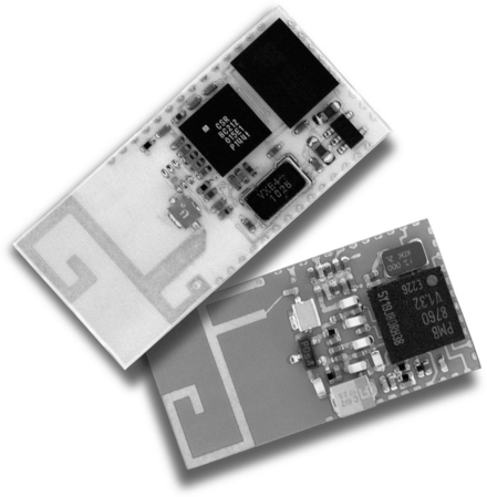
Figure 6.9 presents a Wireless Local Area Network (WLAN) module fully integrated by EPCOS into one SMD chip ready to be mounted in a telephone, MP3 player, laptop or any other portable device. This 8.2 mm × 5.5 mm × 1.4 mm single package contains a RF front end, a power amplifier, a low-noise amplifier and a WLAN radio Integrated Circuit (IC) (Transceiver, Baseband/MAC), and compared to discrete solutions, saves around 80% in PCB space (EPCOS AG, 2006).
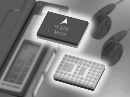
6.9 A WLAN module with integrated RF front end, power amplifier, low-noise amplifier and radio IC (courtesy and copyright of TDK-EPC).
An example of planar, liquid-cooled and electronically steerable antennas for mobile applications, including satellite communications in the Ka band on ships, cars and airplanes, manufactured by IMST, is presented in Fig. 6.10. This application shows that the possibility of embedding microfluidic channels inside circuit boards for active cooling has already come to realisation in LTCC technology.
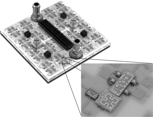
6.10 A planar, liquid-cooled electronically steerable antenna for Ka-band communication (courtesy and copyright of IMST GmbH).
Due to its high reliability and resistance to harsh environments, LTCC is used where normal methods fail – i.e. in engine control units, transmission control, electric power steering, electronic stability control, or dual-clutch transmissions (Murata, 2006). A mass-flow sensor for fuel injection control was presented (Schmid, 2002), as well as a pressure sensor (Fonesca et al., 2002) capable of working at high temperatures. Other LTCC applications in the automotive industry include on-board electronics such as sound and television systems, telecommunication, global positioning systems, but also a short-range radar system for driving assistance.
LTCC structures have also gone many times into space, including voyages to Mars and Jupiter (Scrantom and Gravier, 2000). They are used for satellite communications (Kulke et al., 2009) and many scientific space programmes (Barry LTCC, 2010).
6.4.2 Other areas of application
While industry is already quite familiar with LTCC technology, scientists are constantly working on new applications. Currently, such areas as microsystem packaging, microfluidics, sensors and actuators, optoelectronics and even micro-propulsion are being investigated.
Recent developments in microsystem technologies, mainly in silicon-based chips, have created a need for versatile packaging technology that could connect the chip in all ways necessary, still ensuring good mechanical stability and hermetic sealing. LTCC technology provides the answer to that problem, as it allows not only fine-line electrical connections, but also buried channels, valves and micropumps, freestanding cantilevers, membranes and even optical features. An example of using LTCC technology for silicon microfluidic packaging was presented by Sandia National Laboratories (2007). The connection between silicon and LTCC was secured with screen-printed O-ring seals, which ensured that no fluid leaks out from the joint, while the buried channels allowed a smooth transfer from microscale to standard fluidic connections.
LTCC technology is also feasible for manufacturing different sensors and actuators. Sensors such as flow sensors (Gongora-Rubio et al., 1999), millinewton force sensors (Birol et al., 2007) and temperature sensors (Hrovat et al., 2005) can be manufactured in LTCC. It is also possible to manufacture more complicated structures such as heavy metal detection sensors (Gongora-Rubio et al., 2004), chloride detection sensors (Ibañez-Garcia et al., 2006), phenolic compound sensors (Goldbech et al., 2006) or urea detection sensors (Malecha et al., 2009). Moreover, this technology allows integration of different sensors on one substrate, creating complex lab-on-chip modules (Smetana et al., 2007).
In some cases, valves and pumps are needed to manage the flow correctly. An example of a flow injection analysis LTCC module is presented in Fig. 6.11.

6.11 An example of flow injection analysis LTCC module (Gongora-Rubio et al., 2001).
The presented structure includes reagent, sample and carrier inlets, a reaction coil and a multielectrode sensor for electrochemical measurement. Equipped with electromagnetic valves and a pump, this structure is capable of dosing reagents in the right proportions, mixing them and measuring the product of the reaction. Benefits of using LTCC-based microlaboratories include shorter analysis times as well as a smaller amount of reactants and waste.
Actuator applications in LTCC usually employ the piezoelectric effect or the electromagnetic effect to convert an electrical signal into mechanical displacement, although other structures that harness, e.g. electrostatic force, have been presented. Actuator applications include leaf spring actuators (Newborn et al., 2006), piezoelectric unimorph valves (Sobocinski et al., 2009), piezoelectric cantilevers (Heionen et al., 2007), piezoelectric optical fiber aligning devices (Park et al., 2010), electromagnetic hybrid valves (Gongora-Rubio et al., 1999), micropumps (Gongora-Rubio et al., 2001) and electrostatic valves (Klumbies et al., 2009).
New applications for space technology include solid-state micropropellers (Zhang et al., 2005; Thakur et al., 2010). Ignition by electrical impulse produces a large amount of gases to propel the structure. Thanks to their small size and low cost, arrays of these devices can be mounted on spacecrafts for position corrections. Further investigations will include possibilities of refills.
Energy harvesting structures based on LTCC are also being investigated. A multilayer coil inducer in a vibration-based electromagnetic meso-generator was presented by Hwang et al. (2010). The structure consisted of suspended thick-film multilayer coils with a seismic mass in the centre and a rare-earth magnet attached to the bottom of the structure. Under external vibrations, the seismic mass moved the coils up and down in the static magnetic field of the permanent magnet, generating a current in the coil circuit. An output of 6.46 μW/mm3 was generated with 1 g (9.81 m/s2) acceleration.
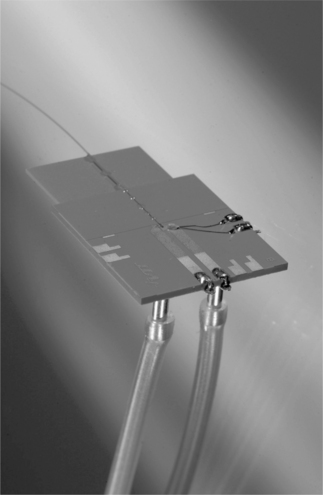
Progress has been made in introducing optical components into LTCC, such as transparent glass windows (Tan et al., 2007; Sandia National Laboratories, 2007), co-fired optical fibres (Lautzenhiser and Amaya, n. d.) and others. An example of such application is shown in Fig. 6.12. A liquid-cooled, fibre-pigtailed package for a high-power laser diode was manufactured by VTT. Passive alignment methods allowed average coupling efficiency at a level of 0.31 with multimode optical fibre.
Another interesting application, presented by Sandia National Laboratories, is an ion mobility spectrometer, presented in Fig. 6.13. In this case, LTCC sheets were rolled after screen printing and laminated into a tube, forming a 3D structure. This solution allowed the use of only three layers instead of 300 (Sandia National Laboratories, 2007). The complete structure included an ioniser, a precise voltage divider, an ion drift chamber, an embedded thick-film heater for ensuring the right operating temperature and a nickel-plated kovar target. The tube ensured hermeticity, proper gas handling and shielding from radioactive material used in the ioniser.
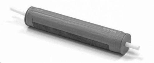
6.13 Portable ion mobility spectrometer (Sandia National Laboratories, 2007).
As shown in this chapter, thanks to its advantages, LTCC technology covers a large range of applications in both everyday use and specially tailored applications. The constant evolution of this technology makes new applications possible and improves those already existing.
6.5 Future trends
Recent development in LTCC technology has been enormous. Particularly interesting possibilities will be created by novel functional LTCC materials, enhanced processes and constantly widening application areas. However, further research is needed to manage the chemical, physical and electrical properties of the materials, i.e. modifying the compound with better chemistry without degrading either physical or electrical properties. Process enhancement may include even lower processing temperatures, tightly controlled shrinkage, higher tolerances of conductors, vias, etc. without increasing processing time. Application areas should spread to MEMS, lab-on-chips, highly integrated systems-on-a-package, autonomous sensors and energy harvesting, among others.
6.6 Sources of further information
The interested reader is guided to the following literature, which provides more information on LTCC technology. This is not a complete list (there are far too many other excellent publications available), but it quite neatly summarises the area of LTCC:
• Imanaka, Multilayered Low Temperature Cofired Ceramics (LTCC) Technology, 2005.
• Mistler and Twiname Tape Casting, Theory and Practice, 2000
• http://www.electroscience.com
• www.ltcc.de – homepage of IMST Gmbh
6.7 References
Andrijasevic, D., Smetana, W., Zehetner, J., Zoppel, S., Brenner, W. Aspects of micro structuring low temperature co-fired ceramic (LTCC) for realization of complex 3D objects by embossing. Microelectronic Engineering. 2007; 84:1198–1201.
Barlow, F., Wood, J., Elshabini, A., Stephens, E.F., Feeler, R., et al. Fabrication of precise fluidic structures in LTCC. International Journal of Applied Ceramic Technology. 2009; 6:18–23.
Barry, L.T.C.C. MetroGroup USA. Available at: http://www.barryltcc.com, 2010. [(accessed 26 August 2010)].
Birol, H., Maeder, T., Jacq, C., Ryser, P. Investigation of interactions between co-fired LTCC components. Journal of the European Ceramic Society. 2005; 25:2065–2069.
Birol, H., Maeder, T., Ryser, P. Influence of processing and conduction materials on properties of co-fired resistors in LTCC structures. Journal of the European Ceramic Society. 2006; 26:1937–1941.
Birol, H., Maeder, T., Nadzeyka, I., Boers, M., Ryser, P. Fabrication of a millinewton force sensor using low temperature co-fired ceramic (LTCC) technology. Sensors and Actuators A: Physical. 2007; 334–338.
Block, C., Fluhr, H., Wiesbauer, K., Riedler, J., Ragossnig, H., et al, Circuit, switching module comprising the same, and use of said switching module. United States Patent 7 343 137. 2008.
Corbett, S., Strole, J., Johnston, K. Direct-write laser exposure of photosensitive conductive inks using shaped-beam optics. International Journal of Applied Ceramic Technology. 2005; 2:390–400.
Deleniv, A., Gevorgian, S., Jantunnen, H., Hu, T., LTCC compatible ferroelectric phase shifters. Microwave Symposium Digest, 2005. IEEE MTT-S International, Long Beach, CA, 2005.
EPCOS, A.G. Components Magazine – EPCOS AG. Available at: http://www.epcos.com/web/generator/Web/Sections/Components/Page,locale=en,r=247996,a=367940.html, 2006. [(accessed 19 July 2010)].
Espinoza-Vallejos, P., Santiago-Aviles, J. Photolithographic feature fabrication in LTCC. International Journal of Microcircuits and Electronic Packaging. 2000; 23:286–292.
Gongora-Rubio, M., Sola-Laguna, L., Santiago-Aviles, J.J., Meso (intermediate)-scale electromechanical systems for the measurement and control of sagging in LTCC structures. Materials Research Society Symposium Proceedings, San Francisco. 1998.
Feingold, A.H., Heinz, M., Wahlers, R.L., Stein, M.A., Materials for capacitive and inductive components integrated with commercially available LTCC systems. Proceedings of the 3rd Annual Conference on Microelectronics and Packaging IMAPS Herzelia. 2003.
Fonseca, M.A., English, J.M., von Arx, M., Allen, M.G. Wireless micromachined ceramic pressure sensor for high-temperature applications. Journal of Microelectromechanical Systems. 2002; 11(4):337–343.
Fournier, Y., Maeder, T., Boutinard-Rouelle, G., Barras, A., Craquelin, N., et al. Integrated LTCC pressure/flow/temperature multisensor for compressed air diagnostics. Sensors. 2010; 10:11 156–11 173.
Ganne, J.-P., Lebourgeois, R., Paté, M., Dubreuil, D., Pinier, L., et al. The electromagnetic properties of Cu-substituted garnets with low sintering temperature. Journal of the European Ceramic Society. 2007; 27:2771–2777.
Goldbach, M., Axthelm, H., Keusgen, M. LTCC-based microchips for the electrochemical detection of phenolic compounds. Sensors and Actuators B: Chemical. 2006; 120:346–351.
Golonka, L., Zastosowanie Ceramiki LTCC w Mikroelektronice, 2001. [Wroclaw].
Golonka, L.J., Roguszczak, H., Zawada, T., Radojewski, J., Grabowska, I., et al. LTCC based microfluidic systems with optical detection. Sensors and Actuators B. 2005; 111–112:396–402.
Gongora-Rubio, M.R., Espinoza-Vallejos, P., Sola-Laguna, L., Santiago-Avilés, J.J. Overview of low temperature co-fired ceramics tape technology for meso-system technology (MsST). Sensors and Actuators A: Physical. 2001; 89:222–241.
Gongora-Rubio, M.R., Fontes, M.B.A., Rocha, Z.M. d, Richter, E.M., Angnes, L. LTCC manifold for heavy metal detection system in biomedical and environmental fluids. Sensors and Actuators B: Chemical. 2004; 103:468–473.
Gongora-Rubio, M.R., Solá-Laguna, L.M., Moffett, P.J., Santiago-Avilés, J.J. The utilization of low temperature co-fired ceramics (LTCC-ML) technology for meso-scale EMS, a simple thermistor based flow sensor. Sensors and Actuators A: Physical. 1999; 73:215–221.
Gongora-Rubio, M.R., Solá-Laguna, L.M., Smith, M., Santiago, J.J.A., A meso-scale electromagnetically actuated normally closed valve realized on LTCC tapes. Proceedings of SPIE Conference on Microfluidic Devices and Systems II. SPIE, Santa Clara, 1999.
Gurauskis, J., Sanchez-Herencia, A.J., Baudin, C. Joining green ceramic tapes made from water-based slurries by applying low pressures at ambient temperature. Journal of the European Ceramic Society. 2005; 25:3403–3411.
Haertling, G.H. Properties of hot-pressed ferroelectric alkali niobate ceramics. Journal of the American Ceramic Society. 1967; 50:329–330.
Hagen, G., Rebenklau, L., Fabrication of smallest vias in LTCC tape. Electronics System Integration Technology Conference, Dresden. 2006.
Heinonen, E., Juuti, J., Jantunen, H. Characteristics of piezoelectric cantilevers embedded in LTCC. Journal of the European Ceramic Society. 2007; 27:4135–4138.
Honkamo, J., Hannu, J., Jantunen, H., Moilanen, M., Mielcarek, W. Microstructural and electrical properties of multicomponent varistor ceramics with PbO–ZnO–B2O3 glass addition. Journal of Electroceramics. 2007; 18:175–181.
Horvth, E. Embedded thick-film resistors applied in low temperature co-fired ceramic circuit substrates. Periodica Polytechnica, Electrical Engineering. 2008; 52:45–57.
Howatt, G.N., Breckenridge, R.G., Brownlow, J.M. Fabrication of thin ceramic sheets for capacitors. Journal of the American Ceramic Society. 1947; 30:237–242.
Hrovat, M., Belavič, D., Kita, J., Cilenšek, J., Golonka, L., et al. Thick-film temperature sensors on alumina and LTCC substrates. Journal of the European Ceramic Society. 3443–3450, 2005.
Hrovat, M., Holc, J., Drnovšek, S., Belavič, D., Cilenšek, J., et al. PZT thick-films on LTCC substrates with an interposed alumina barrier layer. Journal of the European Ceramic Society. 2006; 26:897–900.
Hrovat, M., Belavic, D., Ursic, H., Kita, J., Holc, J., et al, An investigation of thick-film materials for temperature and pressure sensors on self-constrained LTCC substrates. Second Electronics System-Integration Technology Conference, ESTC, Greenwich, 2008. 2008.
Hsi, C.-S., Chen, Y.-C., Jantunen, H., Wu, M.-J., Lin, T.-C. Barium titanate based dielectric sintered with a two-stage process. Journal of the European Ceramic Society. 2008; 28:2581–2588.
Hsi, C.-S., Chen, D.-F., Shieh, F.-M., Fu, S.-L. Processing of LTCC with embedded RuO2-based resistors. Materials Chemistry and Physics. 2003; 78:67–72.
Hwang, Y.M., Lu, W.L., Pan, C.T. Development and fabrication of an LTCC multilayer coil inducer in a vibration-based electromagnetic meso-generator. Microelectronics Journal. 2010; 41:338–346.
Ibañez-Garcia, N., Gonçalves, R.D.M., Rocha, Z.M. d, Góngora-Rubio, M.R., Seabra, A.C., et al. LTCC meso-analytical system for chloride ion determination in drinking waters. Sensors and Actuators B: Chemical. 2006; 118:67–72.
Imanaka, Y. Multilayered Low Temperature Cofired Ceramics (LTCC) Technology. USA: Springer; 2005.
Jaeger, R.E., Egerton, L. Hot pressing of potassium-sodium niobates. Journal of the American Ceramic Society. 1962; 45:209–213.
Jantunen, H., Kangasvieri, T., Vähäkangas, J., Leppävuori, S. Design aspects of microwave components with LTCC technique. Journal of the European Ceramic Society. 2003; 23:2541–2548.
Jantunen, H., Hu, T., Uusimäki, A., Leppävuori, S. Ferroelectric LTCC for multilayer devices. Journal of Ceramic Society of Japan. 2004; 112:1552–1556.
Jean, J.-H., Lin, S.-C. Low-fire processing of ZrO2–SnO2–TiO2 ceramics. Journal of the American Ceramic Society. 2000; 83:1417–1422.
Joshi, H., Sigmarsson, H.H., Peroulis, D., Chappell, W.J., Highly loaded evanescent cavities for widely tunable high-Q filters. Microwave Symposium IEEE/MTT-S International. 2007.
Jurkow, D., Roguszczak, H., Golonka, L. Cold chemical lamination of ceramic green tapes. Journal of the European Ceramic Society. 2009; 29:703–709.
Karioja, P., Keränen, K., Kautio, K., Ollila, J., Heikkinen, M., et al, LTCC-based differential photo acoustic cell for ppm gas sensing. Proceedings of the SPIE San Francisco. 2010.
Khoong, L.E., Tang, Y.M., Lam, Y.C. Overview on fabrication of three-dimensional structures in multi-layer ceramic substrate. Journal of the European Ceramic Society. 2010; 30:1973–1987.
Kim, B.-Y., Han, D.-B., Jeong, C.-W. Preparation of screen printable conductive MoSi2 thick-films for ceramic sheet heater. Journal of the Korean Ceramic Society. 2010; 47:319–324.
Kim, D.-W., Kim, T.-G., Hong, K.S. Low-firing of CuO-doped anatase. Materials Research Bulletin. 1999; 34:771–781.
Kim, H., Shrout, T., Rindall, C., Langan, M. Low temperature sintering and properties of Ag(Nb, Ta)O3 composite ceramics. Journal of the American Ceramic Society. 2002; 85:2738–2744.
Kita, J., Dziedzic, A., Golonka, L.J., Zawada, T. Laser treatment of LTCC for 3D structures and elements fabrication. Microelectronics International. 2002; 19:14–18.
Kittilä, M., Hagberg, J., Jakku, E., Leppävuori, S. Direct gravure printing (DGP) method for printing fine-line electrical circuits on ceramics. IEEE Transactions on Electronics Packaging Manufacturing. 2004; 27:109–114.
Klumbies, H., Partsch, U., Goldberg, A., Gebhardt, S., Actuators to be integrated in low temperature cofired ceramics. ISSE 2009 thirty-second International Spring Seminar on Electronics Technology. 2009. [Brno, Czech Republic].
Knickerbocker, S.H., Kumar, A.H., Herron, L.W. Cordierite glass–ceramics for ceramic packaging. American Ceramic Society Bulletin. 1993; 72:90–95.
Kok, S.L., White, N., Harris, N. Fabrication and characterisation of free-standing thick-film piezoelectric cantilevers for energy harvesting. Measurement Science and Technology. 2009; 20:124 010–124 023.
Kulke, R., Wahle, V., Sollbach, D., Uhlig, P., Rittweger, M., et al, High level of integration for Bluetooth modules on LTCC. Fourteenth European Microelectronics and Packaging Conference and Exhibition. 2003. [Friedrichshafen].
Kulke, R., Möllenbeck, G., Günner, C., Uhlig, P., Drüe, K.H., et al. Ceramic microwave circuits for satellite communication. Journal of Microelectronics and Electronic Packaging. 2009; 6:27–31.
Kyocera. LTCC Packages for RF Modules | Semiconductor Components | Products | KYOCERA. Available at: http://global.kyocera.com/prdct/semicon/semi/ltcc/index.html, 2007. [(accessed 19 July 2010)].
Lautzenhiser, F., Amaya, E. HeraLock 2000 Self-constrained LTCC Tape. Heraeus CMD; 2002.
Lee, Y.-C., Lin, C.-H., Lin, I.-N. Bi-Zn-Nb-O microwave dielectric materials for multilayer filter application. Materials Chemistry and Physics. 2003; 79:124–128.
Li, J.-F., Wang, K., Zhang, B.-P., Zhang, L.-M. Ferroelectric and piezoelectric properties of fine-grained Na0.5K0.5NbO3 lead-free piezoelectric ceramics prepared by spark plasma sintering. Journal of the American Ceramic Society. 2006; 89:706–709.
Lim, K., Pinel, S., Davis, M., Sutono, A., Lee, C.-H., et al. RF-System-on-package (SOP) for wireless comunnications. IEEE Microvawe Magazine. 2002; 3(1):88–94.
Lin, Y.-S., Liu, C.-C., Li, L.-M., Chen, C.-H. Design of an LTCC tri-band transceiver module for GPRS mobile applications. IEEE Transactions on Microwave Theory and Techniques. 2004; 52:2718–2724.
Lisjak, D., Drofenik, M. Influence of Ag on the composition and electromagnetic properties of low-temperature cofired hexaferrites. Journal of the American Ceramic Society. 2007; 90:3121–3126.
Malecha, K., Pijanowska, D.G., Golonka, L.J., Torbiczb, W. LTCC microreactor for urea determination in biological fluids. Sensors and Actuators B: Chemical. 2009; 141:301–308.
Marques, V.M.F., Tulyaganov, D.U., Agathopoulos, S., Gataullin, V.K., Kothiyal, G.P., et al. Low temperature synthesis of anorthite based glass-ceramics via sintering and crystallization of glass-powder compacts. Journal of the European Ceramic Society. 2006; 26:2503–2510.
Matz, R., Götsch, D., Karmazin, R., Männer, R., Siessegger, B. Low temperature cofirable MnZn ferrite for power electronic applications. Journal of Electroceramics. 2009; 22:209–215.
Maw, H.P., Wai, S.C., Tjeung, R.T., Wai, L.C., Keng, L.B., et al, Microembossing of LTCC (low temperature co-fired ceramic) green substrates. Ninth Electronics Packaging Technology Conference Singapore. 2007.
Mikeska, K.R., Schaefer, D.T., Jensen, R.H., Method for reducing shrinkage during firing of green ceramic bodies. United States Patent No. 5085720. 1992.
Mis, E., Dziedzic, A., Mielcarek, W. Microvaristors in thick-film and LTCC circuits. Microelectronics Reliability. 2009; 49:607–613.
Mistler, R.E., Twiname, E.R. Tape Casting, Theory and Practice. Westerville: American Ceramic Society; 2000.
Murata, (Press release) Making great contributions to realize the intelligent cars. (‘Technologies of Murata’) Tech-On!. 2006 Available at:. http://www.murata.com/auto/techon/solution_5–5.html [(accessed 19 July 2010)].
Nagata, H. Electrical properties and tracer diffusion of oxygen in some Bi-based lead-free piezoelectric ceramics. Journal of the Ceramic Society of Japan. 2008; 116:271–277.
Nahm, C.-W. Effect of sintering temperature electrical properties of ZNR doped with Pr–Co–Cr–La. Ceramics International. 2008; 34:1521–1525.
Newborn, C.H., English, J.M., Coe, D.J. LTCC fabrication for a leaf spring vertical actuator. International Journal of Applied Ceramic Technology. 2006; 3:61–67.
Ohata, K., Maruhashi, K., Ito, M., Kishimoto, S., Ikuina, K., et al, 1.25 Gbps wireless Gigabit Ethernet link at 60 GHz-band. IEEE MTT-S International Microwave Symposium Digest. 2003. [Philadelphia].
Park, S.-H., Baker, A., Eitel, R.E., Randall, C.A., Uchino, K. Active optical fiber alignment with a piezoelectric ultrasonic motor integrated into low temperature cofired ceramics. Journal of Intelligent Material Systems and Structures. 2010; 21:469–479.
Park, J., Espinoza-Vallejos, P., Sola-Laguna, L., Santiago-Aviles, J., Etching and exfoliation techniques for the fabrication of 3-D meso-scale structures on LTCC tapes. Proceedings SPIE 3582 (International Society for Optical Engineering) San Diego. 1998.
Peterson, K.A., Patel, K.D., Ho, C.K., Rohde, S.B., Nordquist, C.D., et al. Novel microsystem applications with new techniques in low-temperature co-fired ceramics. International Journal of Applied Ceramic Technologies. 2005; 2:345–363.
Piwonski, M.A., Roosen, A. Low pressure lamination of ceramic green tapes by gluing at room temperature. Journal of the European Ceramic Society. 1999; 19:263–270.
Rabe, T., Kuchenbecker, P., Schulz, B. Hot embossing: an alternative method to produce cavities in ceramic multilayer. International Journal of Applied Ceramic Technology. 2007; 4:38–46.
Rabe, T., Schiller, W.A., Hochheimer, T., Modes, C., Kipka, A. Zero shrinkage of LTCC by self-constrained sintering. International Journal of Applied Ceramic Technology. 2005; 2(5):374–382.
Rhim, S.H., Shin, S.Y., Joo, B.Y., Oh, S.I. Burr formation during micro via-hole punching process of ceramic and PET double layer sheet. International Journal of Advanced Manufacturing Technologies. 2006; 30:227–232.
Roosen, A. New lamination technique to join ceramic green tapes for the manufacturing of multilayer devices. Journal of the European Ceramic Society. 2001; 21:1993–1996.
Sandia National Laboratories. Macro–Meso–Microsystems Integration in LTCC LDRD. Albuquerque: Sandia National Laboratories; 2007.
Schmid, U. A robust flow sensor for high pressure automotive applications. Sensors and Actuators A: Physical. 2002; 97–98:253–263.
Scrantom, C., Gravier, G., LTCC Technology. Where We Are and Where We’re Going IV. Costa Mesa, California, 2000.
Sebastian, M., Jantunen, H. Low loss dielectric materials for LTCC applications: a review. International Materials Reviews. 2008; 53:57–90.
Shamim, A., Bray, J., Roy, L., Hojjat, N., Abou Elasoued, R., et al, Microwave and magnetostatic characterization of ferrite LTCC for tunable and reconfiguarable SiP applications. Microwave Symposium IEEE/MTT-S International Honolulu. 2007.
Smetana, W., Balluch, B., Stangl, G., Gaubitzer, E., Edetsberger, M., et al. A multi-sensor biological monitoring module built up in LTCC-technology. Microelectronic Engineering. 2007; 84:1240–1243.
Sobocinski, M., Juuti, J., Jantunen, H., Golonka, L. Piezoelectric unimorph valve assembled on an LTCC substrate. Sensors and Actuators A: Physical. 2009; 149:315–319.
Sobocinski, M., Tadaszak, R., Golonka, L., Cofired optical fiber in LTCC. Thirty-second International IMAPS-IEEE CPMT Poland Conference. 2008.
Steinberg, J.I., Horowitz, S.J., Bacher, R.J. Low-temperature co-fired tape dielectric material systems for multilayer interconnections, advances in ceramics. Multilayer Ceramic Devices. 1998; 19:31–39.
Sun, N.X., Wang, J.W., Daigle, A., Pettiford, C., Mosallaei, H., et al. Electronically tunable magnetic patch antennas with metal magnetic films. Electronics Letters. 2007; 43:434–436.
Sunppan, V., Vadiveloo, P.L., Wai, L.L., Fan, W., Lu, C.W., Processing and electrical characterization of co-sintered composite glass ceramics. Eighth Electronics Packaging Technology Conference Singapore. 2006.
Takao, H., Saito, Y., Aok, Y., Horibuchi, K. Microstructural evolution of crystalline-oriented (K0.5Na0.5)NbO3 piezoelectric ceramics with a sintering aid of CuO. Journal of the American Ceramic Society. 2006; 89:1951–1956.
Tan, Y.M., Khoong, L.E., Lam, Y.C., Lu, C.W., Integration of glass layer for meso and micro-system applications. Ninth Electronics Packaging Technology Conference. 2007. [Singapore].
Thakur, J., Pratap, R., Fournier, Y., Maeder, T., Ryser, P. Realization of a solid-propellant based microthruster using low temperature co-fired ceramics. Sensors and Transducers Journal. 2010; 117:29–40.
Tick, T., Palukuru, V., Komulainen, M., Peräntie, J., Jantunen, H. Method for manufacturing embedded variable capacitors in low-temperature cofired ceramic substrate. Electronics Letters. 2008; 44:94–95.
Tummala, R.R. Ceramic and glass-ceramic packaging in the 1990s. Journal of the American Ceramic Society. 1991; 74:895–908.
Udovic, M., Valant, M., Suvorov, D. Phase formation and dielectric characterization of the Bi2O3–TeO2 system prepared in an oxygen atmosphere. Journal of the American Ceramic Society. 2004; 87:591–597.
Valant, M., Suvorov, D. Low-temperature sintering of (Ba0.6Sr0.4)TiO3. Journal of the American Ceramic Society. 2004; 87:1222–1226.
Vanek, J., Smetana, W., Weilguni, M., Szendiuch, I., Characterization of PTC resistor pastes applied in LTCC technology. Proceedings of the European Microelectronics and Packaging Conference EMPC. 2009. [Rimini].
Wang, G., Barlow, F., Elshabini, A., Modeling and control of resistance tolerance for embedded resisotrs in LTCC. Proceedings of Fifty-Second Electronic Components and Technology Conference. 2002. [San Diego].
Wang, G., Folk, E.C., Barlow, F., Elshabini, A. Fabrication of Microvias for Multilayer LTCC Substrates. IEEE Transactions on Electronics Packaging Manufacturing. 2006; 29:32–41.
Wang, Y.L., Ollivier, P.J., Skurski, M.A., Photoformed thick-film materials and their application to fine feature circuitry. HDI Conference. 2000. [Denver].
Yan, M., Hu, J., Luo, W., Zhang, W.Y. Preparation and investigation of low firing temperature NiCuZn ferrites with high relative initial permeability. Journal of Magnetism and Magnetic Materials. 2006; 303:249–255.
Yau, Y.-W., Booke, M.A., Sandhu, N.S., Fulton, J.J., Microelectronics packaging processing using focused high power electron beams. Proceedings of Forty-First Electronic Components and Technology Conference Atlanta. 1991.
Yau, Y.-W., Long, D.C., Grant, W.T., Sandhu, N.S., Fulton, J.J., Overview of via formation technologies for ceramic packaging manufacturing. Proceedings of Forty-Third Electronic Components and Technology Conference Orlando. 1993.
Yokoi, A., Ogawa, H., Kan, A. Microwave dielectric properties of Mg4Nb2O9–3.0 wt.% LiF ceramics prepared with CaTiO3 additions. Journal of the European Ceramic Society. 2005; 25:2871–2875.
Zampino, M.A., Kandukuri, R., Kinzy Jones, W., High performance thermal vias in LTCC substrates. Proceedings 2002 Inter Society Conference on Thermal Phenomena San Diego. 2002.
Zhang, K.L., Chou, S.K., Ang, S.S. Development of a low-temperature co-fired ceramic solid propellant microthruster. Journal of Micromechanics and Microengineering. 2005; 15:944–952.
Zhang, Q.-L., Yang, H., Tong, J.-X. Low-temperature firing and microwave dielectric properties of MgTiO3 ceramics with Bi2O3–V2O5. Materials Letters. 2006; 60:1188–1191.
Zhao, F., Yue, Z., Lin, Y., Gui, Z., Li, L. Phase relation and microwave dielectric properties of xCaTiO3–(1–x)TiO2–3ZnTiO3 multiphase ceramics. Ceramics International. 2007; 33:895–900.